EP4128650B1 - System and method for sparse data synchronization and communication - Google Patents
System and method for sparse data synchronization and communication Download PDFInfo
- Publication number
- EP4128650B1 EP4128650B1 EP21718234.4A EP21718234A EP4128650B1 EP 4128650 B1 EP4128650 B1 EP 4128650B1 EP 21718234 A EP21718234 A EP 21718234A EP 4128650 B1 EP4128650 B1 EP 4128650B1
- Authority
- EP
- European Patent Office
- Prior art keywords
- signals
- stream
- serial
- parallel
- synchronization
- Prior art date
- Legal status (The legal status is an assumption and is not a legal conclusion. Google has not performed a legal analysis and makes no representation as to the accuracy of the status listed.)
- Active
Links
Images


Classifications
-
- H—ELECTRICITY
- H04—ELECTRIC COMMUNICATION TECHNIQUE
- H04B—TRANSMISSION
- H04B10/00—Transmission systems employing electromagnetic waves other than radio-waves, e.g. infrared, visible or ultraviolet light, or employing corpuscular radiation, e.g. quantum communication
- H04B10/70—Photonic quantum communication
-
- H—ELECTRICITY
- H04—ELECTRIC COMMUNICATION TECHNIQUE
- H04B—TRANSMISSION
- H04B10/00—Transmission systems employing electromagnetic waves other than radio-waves, e.g. infrared, visible or ultraviolet light, or employing corpuscular radiation, e.g. quantum communication
- H04B10/11—Arrangements specific to free-space transmission, i.e. transmission through air or vacuum
- H04B10/112—Line-of-sight transmission over an extended range
- H04B10/1121—One-way transmission
-
- H—ELECTRICITY
- H04—ELECTRIC COMMUNICATION TECHNIQUE
- H04B—TRANSMISSION
- H04B10/00—Transmission systems employing electromagnetic waves other than radio-waves, e.g. infrared, visible or ultraviolet light, or employing corpuscular radiation, e.g. quantum communication
- H04B10/11—Arrangements specific to free-space transmission, i.e. transmission through air or vacuum
- H04B10/112—Line-of-sight transmission over an extended range
- H04B10/1123—Bidirectional transmission
-
- H—ELECTRICITY
- H04—ELECTRIC COMMUNICATION TECHNIQUE
- H04B—TRANSMISSION
- H04B10/00—Transmission systems employing electromagnetic waves other than radio-waves, e.g. infrared, visible or ultraviolet light, or employing corpuscular radiation, e.g. quantum communication
- H04B10/25—Arrangements specific to fibre transmission
- H04B10/2575—Radio-over-fibre, e.g. radio frequency signal modulated onto an optical carrier
- H04B10/25752—Optical arrangements for wireless networks
- H04B10/25753—Distribution optical network, e.g. between a base station and a plurality of remote units
- H04B10/25755—Ring network topology
-
- H—ELECTRICITY
- H04—ELECTRIC COMMUNICATION TECHNIQUE
- H04B—TRANSMISSION
- H04B10/00—Transmission systems employing electromagnetic waves other than radio-waves, e.g. infrared, visible or ultraviolet light, or employing corpuscular radiation, e.g. quantum communication
- H04B10/60—Receivers
- H04B10/66—Non-coherent receivers, e.g. using direct detection
- H04B10/69—Electrical arrangements in the receiver
-
- H—ELECTRICITY
- H04—ELECTRIC COMMUNICATION TECHNIQUE
- H04J—MULTIPLEX COMMUNICATION
- H04J14/00—Optical multiplex systems
- H04J14/02—Wavelength-division multiplex systems
-
- H—ELECTRICITY
- H04—ELECTRIC COMMUNICATION TECHNIQUE
- H04L—TRANSMISSION OF DIGITAL INFORMATION, e.g. TELEGRAPHIC COMMUNICATION
- H04L7/00—Arrangements for synchronising receiver with transmitter
- H04L7/0008—Synchronisation information channels, e.g. clock distribution lines
-
- H—ELECTRICITY
- H04—ELECTRIC COMMUNICATION TECHNIQUE
- H04L—TRANSMISSION OF DIGITAL INFORMATION, e.g. TELEGRAPHIC COMMUNICATION
- H04L7/00—Arrangements for synchronising receiver with transmitter
- H04L7/0075—Arrangements for synchronising receiver with transmitter with photonic or optical means
-
- H—ELECTRICITY
- H04—ELECTRIC COMMUNICATION TECHNIQUE
- H04L—TRANSMISSION OF DIGITAL INFORMATION, e.g. TELEGRAPHIC COMMUNICATION
- H04L7/00—Arrangements for synchronising receiver with transmitter
- H04L7/0079—Receiver details
-
- H—ELECTRICITY
- H04—ELECTRIC COMMUNICATION TECHNIQUE
- H04L—TRANSMISSION OF DIGITAL INFORMATION, e.g. TELEGRAPHIC COMMUNICATION
- H04L7/00—Arrangements for synchronising receiver with transmitter
- H04L7/04—Speed or phase control by synchronisation signals
-
- H—ELECTRICITY
- H04—ELECTRIC COMMUNICATION TECHNIQUE
- H04L—TRANSMISSION OF DIGITAL INFORMATION, e.g. TELEGRAPHIC COMMUNICATION
- H04L7/00—Arrangements for synchronising receiver with transmitter
- H04L7/04—Speed or phase control by synchronisation signals
- H04L7/041—Speed or phase control by synchronisation signals using special codes as synchronising signal
- H04L7/043—Pseudo-noise [PN] codes variable during transmission
-
- H—ELECTRICITY
- H04—ELECTRIC COMMUNICATION TECHNIQUE
- H04L—TRANSMISSION OF DIGITAL INFORMATION, e.g. TELEGRAPHIC COMMUNICATION
- H04L9/00—Cryptographic mechanisms or cryptographic arrangements for secret or secure communications; Network security protocols
- H04L9/001—Cryptographic mechanisms or cryptographic arrangements for secret or secure communications; Network security protocols using chaotic signals
-
- H—ELECTRICITY
- H04—ELECTRIC COMMUNICATION TECHNIQUE
- H04L—TRANSMISSION OF DIGITAL INFORMATION, e.g. TELEGRAPHIC COMMUNICATION
- H04L9/00—Cryptographic mechanisms or cryptographic arrangements for secret or secure communications; Network security protocols
- H04L9/08—Key distribution or management, e.g. generation, sharing or updating, of cryptographic keys or passwords
- H04L9/0816—Key establishment, i.e. cryptographic processes or cryptographic protocols whereby a shared secret becomes available to two or more parties, for subsequent use
- H04L9/0852—Quantum cryptography
-
- H—ELECTRICITY
- H04—ELECTRIC COMMUNICATION TECHNIQUE
- H04L—TRANSMISSION OF DIGITAL INFORMATION, e.g. TELEGRAPHIC COMMUNICATION
- H04L9/00—Cryptographic mechanisms or cryptographic arrangements for secret or secure communications; Network security protocols
- H04L9/12—Transmitting and receiving encryption devices synchronised or initially set up in a particular manner
-
- H—ELECTRICITY
- H04—ELECTRIC COMMUNICATION TECHNIQUE
- H04L—TRANSMISSION OF DIGITAL INFORMATION, e.g. TELEGRAPHIC COMMUNICATION
- H04L9/00—Cryptographic mechanisms or cryptographic arrangements for secret or secure communications; Network security protocols
- H04L9/40—Network security protocols
Definitions
- the present application is generally in the field of synchronization and communication of sparse data transmission, such as in single-photon quantum communication applications.
- a standard telecommunication transceiver can detect signals of rates higher than 25Gbps, which means that it can measure events (e.g., bit arrival) within time intervals shorter than 40ps.
- the synchronization task (accurate time slot assignment of the received signals) in such standard communication systems is relatively simple because the intensity of the communicated signals is typically strong and easily detected by the receiver, which can be used to regenerate the clock signal of the transmitter (Tx) and operate the receiver (Rx) at the same clock frequency of the transmitter.
- utilizing such standard communication systems to implement an event timing system requires provision of a balanced stream of data from the transmitter to the receiver, in order to enable proper clock data recovery (CDR) functionality of the receiver, and reduction of the received data rate (also referred to herein as data speed conversion e . g ., as carried out by a serializer/deserializer - SERDES) for data processing and analysis. If, however, this condition cannot be maintained, the synchronization between the transmitter and receiver is lost.
- CDR clock data recovery
- ALAN MINK ET AL "Programmable instrumentation and gigahertz signaling for single-photon quantum communication systems",NEW JOURNAL OF PHYSICS, INSTITUTE OF PHYSICS PUBLISHING, BRISTOL, GB, vol. 11, no. 4, 1 April 2009 (2009-04-01), pages 1-14,ISSN: 1367-2630, DOI: 10.1088/1367-2630/11/4/045016 discloses piggybacking a sparse signal from a single-photon detector on top of a balanced serial data stream. This allows the SerDes to receive the single-photon detection events to synchronize to the clock of the balanced data stream. The parallel data from both SerDes and their recovered clocks are passed to a FPGA, where the balanced data are removed, via an XOR, leaving the detection signal
- a QKD transmission method is disclosed in International Patent Publication No. WO 2012/105930 , wherein a transmission list is generated for a plurality of data bits.
- the transmission list comprises a randomized timing schedule defining respective times for transmission of the data bits, providing a clock signal and using the clock signal to initiate the transmission of the data bits at a predetermined time in order to provide a QKD signal, and an apparatus therefor.
- US Patent Publication No. 2012/294625 discloses a communication system comprising an emitter of weak light pulses, a detector which is capable of detecting single photons, and a source of a clock signal, wherein said emitter and detector are synchronized using said clock signal.
- the system further comprising a frequency divider for said clock signal to produce a reduced frequency clock signal and a clock regenerator for regenerating the original clock signal from the reduced frequency clock signal.
- the system further comprising a communication channel configured to communicate the clock signal between the emitter and detector, the clock signal being reduced before sending through the channel and reconstructed after it has exited the channel.
- US Patent Publication No. 2016/134420 discloses system and methods for synchronizing and aligning quantum channel for Quantum Key Distribution, to allow a Quantum Key Distribution (QKD) apparatus to work continuously with only two communication channels, a quantum communication channel and a service channel. This is achieved by linking the clock frequencies of both channels and completed by an over-sampling method for phase synchronization tracking. Clock signal carry is done through data using clock data recovery encoding techniques. Having a continuous operating QKD system is not possible without a tracking system that enables phase alignment. This synchronization and alignment system and method for QKD has multiple benefits as it allows real-time synchronization with continuous data flow and is not dedicated to a specific quantum protocol.
- Mink Alan et al (“High-speed quantum key distribution system supports one-time pad encryption of real-time video", https://www.spiedigitallibrary.org/conference-proceedings-of-spie on 21 Feb 2021 ) describe a high-speed quantum key distribution (QKD) test bed incorporating both free-space and fiber systems. These systems demonstrate a major increase in the attainable rate of QKD systems: over two orders of magnitude faster than other systems.
- Clock regeneration and data speed conversion functionalities of conventional transceivers are not designed to handle sparse data communication streams. Therefore, sparse data communication systems typically requires specially designed and expensive circuitries for clock synchronization and data recovery, which complicates the system development and production, and entails increased costs.
- the present disclosure provides sparse data communication solutions utilizing readily available/nonspecialized off the shelf circuitries/devices, to thereby alleviate design requirements and production costs of sparse data communication systems.
- a key feature of the present application is the use of manipulating circuitry to introduce reversible redundancy to the data signals received over a sparse data communication channel, and thereby enable use of the functionality of standard transceiver device(s) for clock regeneration (e.g., frequency locking by CDR of the transceiver) and data speed conversion (e.g., by SERDES of the transceiver), for converting the received high speed serial sparse signal stream into a lower rate parallel signal stream, for processing and analysis.
- the redundancy introduced to the sparse serial data is derived from synchronization signals, which is a pseudo random binary sequence - PRBS, indicative of a clock signal used by the transmitter of the sparse data signals.
- the transmitter can send the synchronization signals to the receiver over a separate communication channel (e.g., conventional optical channel using optical fibers, RF channel, or over electric cables).
- the receiver can be accordingly configured to receive the synchronization signals (e.g., by a small form-factor pluggable - SFP module) from the transmitter, and reversibly mix/combine the received synchronization signals with the received sparse serial data signals.
- an external synchronization signal source can be used by the receiver to introduce the redundancy to the sparse serial data signals.
- an internal synchronization signal source generated in the receiver is used to introduce the redundancy to the received sparse data, with or without an external synchronization signal source.
- the synchronization signals used to introduce the redundancy into the received sparse data signals can comprise clock signals having the frequency and periodicity of the clock signal used by the transmitter to transmit the sparse data signals.
- the CDR functionality of a conventional transceiver can be used at the receiver for frequency locking to frequency of an external system, and SERDES of the transceiver can be used for data speed conversion, by producing from the received mixed high speed serial signal stream a lower speed parallel signal stream.
- the clock signal of the synchronization signals comprises a PRBS.
- the synchronization signals can comprise a clock signal that both the transmitter and the receiver lock their frequency to, and convert (e.g., by a phase-locked loop - PLL circuitry) to the correct working frequency, and thereby communicate without requiring an additional (conventional) communication channel.
- the receiver is configured to locally generate the synchronization signals, and use the same to introduce the redundancy to the received sparse data signals for the operation of the transceiver.
- the initial timing of sparse data signals transmission can be obtained using an internal accurate clock device (e.g., global positioning system - GPS clock), or utilizing another synchronization signal from an external source, or communicated between the transmitter and the receiver on the sparse data communication channel e.g., by transmitting to the receiver a higher intensity optical signal for detection without single photon detectors, from the transmitter to the receiver or from the receiver to the transmitter.
- the synchronization signals are generated by the receiver (of the sparse data signals) and transmitted from the receiver to the transmitter (of the sparse data signals).
- the manipulating circuitry is implemented by an external fast serial logical XOR (exclusive OR) gate configured to mix the received sparse data signals with synchronization signals, and feed the mixed signal thereby generated to the receiver for clock regeneration (e . g ., CDR frequency locking) and data speed (e.g., SerDes) conversion.
- an external fast serial logical XOR (exclusive OR) gate configured to mix the received sparse data signals with synchronization signals, and feed the mixed signal thereby generated to the receiver for clock regeneration (e . g ., CDR frequency locking) and data speed (e.g., SerDes) conversion.
- the redundancy introduced to the received sparse data signals can be removed by a parallel logical XOR gate circuitry configured to mix the lower rate parallel (deserialized) mixed signal stream generated by the transceiver (SerDes) with respective parallel regenerated synchronization signal stream produced by the transceiver e.g., an internal PRBS loop controlled by the CDR of the transceiver to have the same frequency and periodicity of the clock signal of the transmitter.
- SerDes serialized mixed signal stream generated by the transceiver
- respective parallel regenerated synchronization signal stream produced by the transceiver e.g., an internal PRBS loop controlled by the CDR of the transceiver to have the same frequency and periodicity of the clock signal of the transmitter.
- a first analog combiner circuitry is used to combine the received sparse data signals with the received synchronization signals, and feed a first combined signal thereby produced to a first transceiver channel for clock regeneration (e.g., by CDR frequency locking) and data speed (e.g., SerDes) conversion
- a second analog combiner circuitry is used to combine the same received sparse data signals with an inverse ( e.g ., utilizing logical inverter/NOT circuitry) of the received synchronization signals and feed a second combined signal thereby generated to a second transceiver channel for clock regeneration ( e.g., by CDR frequency locking) and data speed (e.g., SerDes) conversion.
- An internal logical XOR gate circuitry is used in each of the transceiver channels to perform an intermediate data recovery stage, by mixing the lower rate parallel signal stream produced by its data speed conversion with a corresponding parallel stream of the synchronization signals generated/emulated by its clock regenerator.
- the transmitted data can be then recovered by combining (e.g., utilizing a parallel logical OR gate circuit) the parallel mixed signal streams produced by the logical XOR gate circuitries of the first and second transceiver channels.
- the recovered data transmission i.e., generated by the parallel logical XOR (or OR) gate circuitry
- the data signal pattern for the correlation with the recovered data stream is received in the receiver through another data channel (e.g., LAN).
- the correlation can be carried out in the transceiver, or by an external data processing (computer) system.
- the sparse data communication channel is an optical channel (e.g., optical fiber or free space medium) used for transmission of quantum single-photon qubits.
- a single photon detector can be used at the receiver to convert the received sparse data optical signal into corresponding sparse data electrical signals.
- the synchronization signals communication channel can be implemented by a conventional data communication channel e.g., radio frequency - RF, over electrical cables or optical fibers.
- the synchronization signals communication channel can be implemented by an optical fiber, and the receiver can utilize a small form-factor pluggable (SFP) module to convert the received the optical synchronization signals into corresponding electrical signals.
- SFP small form-factor pluggable
- a sparse data signal receiver comprising a mixer configured to generate a serial stream of mixed signals from a serial stream of sparse data signals and a serial stream of synchronization signals, to thereby add redundancy to the serial stream of sparse data signals and enable clock regeneration therefrom, a clock regeneration unit configured to receive the serial stream of mixed signals, determine based thereon a frequency of the synchronization signals, and generate a stream of parallel synchronization signals emulating the serial stream of synchronization signals, a data speed convertor configured to convert the serial stream of mixed signals into a stream of parallel mixed signals, the streams of parallel signals having a data rate lower than a data rate of the serial signal streams, and a demixer configured to generate a parallel stream of demixed signals from the stream of parallel synchronization signals and the stream of parallel mixed signals and thereby remove the redundancy introduced by the mixer into the sparse data signals.
- the synchronization signals comprise a pseudo random bit stream.
- the serial stream of sparse data signals is received in some embodiments over a single-photon quantum communication channel.
- a single photon detector can be used to receive the serial stream of sparse data signals.
- the regeneration unit and the data speed convertor can be implemented by clock-data recovery (CDR) circuitry and serializer-deserialize (SERDES) circuitry of at least one transceiver channel of a transceiver device.
- the at least one transceiver channel can be used to implement the demixer.
- the mixer can comprise a serial logical XOR gate circuitry and the demixer can comprise a parallel logical XOR gate circuitry.
- the parallel logical XOR circuitry is implemented in the at least one transceiver channel of the transceiver device.
- the mixer can comprise a first analog combiner configured to generate a first serial combined signal from the serial streams of sparse data and synchronization signals, and a second analog combiner configured to generate a second serial combined signal from the serial stream of sparse data signals and an inverse of the serial stream of synchronization signals.
- the CDR, SERDES and parallel XOR gate, circuitries, of respective first and second transceiver channels of the transceiver can be configured to generate respective first and second streams of parallel demixed signals from the first and second combined signals.
- a parallel logical OR gate circuitry can be used to receive the first and second streams of parallel demixed signals from the first and second transceiver channels and remove the redundancy introduced by the mixer into the sparse data signals.
- the mixer comprises a first analog combiner configured to generate a first serial combined signal from the serial streams of sparse data and synchronization signals, and a second analog combiner configured to generate a second serial combined signal from the serial stream of sparse data signals and an inverse of the serial stream of synchronization signals, and wherein SERDES circuitry of respective first and second transceiver channels of the transceiver are configured to generate respective first and second streams of parallel combined signals from the first and second serial combined signals.
- a parallel logical AND gate circuitry can be used to receive the first and second streams of parallel combined signals from the first and second transceiver channels and remove the redundancy introduced by the mixer into the sparse data signals.
- a timing module is used in some embodiments to correlate at least a portion of the stream of parallel demixed signals with a predefined data signal pattern, and determine based thereon a time difference between the serial streams of sparse data and synchronization signals.
- the timing module can be configured and operable to identify missing bits in the PRBS of the serial synchronization signals stream based on the correlation, and correct the timing of the received serial synchronization signals stream accordingly.
- the system comprises in some a service data communication channel.
- the predefined data signal pattern for the correlation can be received over the service data communication channel.
- a tuneable time delay unit is used in some embodiments to affect a time delay to at least one of the serial streams of sparse data and synchronization signals based on the determined time difference.
- the serial stream of synchronization signals is received over an optical communication channel.
- the system can comprise a small form-factor pluggable module configured to receive the serial stream of synchronization signals.
- the optical communication channel comprises a dense wavelength division multiplexing (DWDM) channel.
- the transmitter can be configured in some embodiment to combine data signals with the synchronization signals transmitted over the DWDM channel.
- Another inventive aspect of the subject matter disclose herein relates to communication system comprising the receiver system of any of the embodiments disclosed hereinabove or hereinbelow, a transmitter system comprising a data transmitter for transmitting the stream of sparse data signals, a synchronization signals generator configured to generate the serial stream of synchronization signals, and a synchronization signals transmitter for transmitting the serial stream of synchronization signal, a sparse data signals communication channel for transmitting the stream of sparse data signals to the receiver system, and a synchronization signals communication channel for transmitting the stream of synchronization signals to the receiver system.
- the communication system comprises in some embodiments a service data channel for transmitting to the receiver system a data signal pattern for correlation with at least a portion of the stream of parallel demixed signals to thereby determine a time difference between the serial streams of sparse data and synchronization signals.
- the communication system comprises an external synchronization system configured to generate the stream of synchronization signals and input the same to the receiver and/or the transmitter systems.
- the communication system comprises in some embodiments a GPS clock configured to signal to the receiver and/or the transmitter commencement of transmission of the stream of sparse data signals.
- Yet another inventive aspect of the subject matter disclosed herein relates to a method for synchronization of sparse data signals.
- the method comprising mixing a serial stream of sparse data signals with a serial stream of synchronization signals, to thereby add redundancy to the serial stream of sparse data signals and enable clock regeneration from a serial stream of mixed signals produced by the mixing, emulating the serial stream of synchronization signals by applying the clock regeneration to the serial stream of mixed signals, and generating a stream of parallel synchronization signals having a frequency of the serial stream of synchronization signals, deserializing the serial stream of mixed signals into a stream of parallel mixed signals having a data rate lower than a data rate of the serial signal streams, and demixing the stream of parallel synchronization signals with the stream of parallel mixed signals and thereby removing the redundancy introduced by the mixing into the sparse data signals and generating a parallel stream of demixed signals substantially synchronized with the synchronization signals.
- the mixing comprises in some embodiments serially XORing the serial stream of sparse data signals with the serial stream of synchronization signals.
- the demixing comprises in some embodiments parallelly XORing the stream of parallel synchronization signals with the stream of parallel mixed signals.
- the mixing comprises combining the serial streams of sparse data and synchronization signals and thereby generating a first stream of combined signals, combining the serial stream of sparse data signals and an inverse of the serial stream of synchronization signals and thereby generating a second stream of combined signals, emulating the serial stream of synchronization signals by applying the clock regeneration to the first and second streams of combined signals and generating respective first and second streams of parallel synchronization signals having a frequency of the serial stream of synchronization signals, deserializing the first and second streams of combined signals and generating respective first and second streams of parallel combined signals having a data rate lower than a data rate of the serial signal streams, demixing the first stream of parallel synchronization signals with the first stream of parallel combined signals and thereby generating a first stream of parallel demixed signals, demixing the second stream of parallel synchronization signals with the second stream of parallel combined signals and thereby generating a second stream of parallel demixed signals, and combining by logical OR the first and second streams of parallel
- the mixing comprises combining the serial streams of sparse data and synchronization signals and thereby generating a first stream of combined signals, combining the serial stream of sparse data signals and an inverse of the serial stream of synchronization signals and thereby generating a second stream of combined signals, deserializing the first and second streams of combined signals and generating respective first and second streams of parallel combined signals having a data rate lower than a data rate of the serial signal streams, and combining by logical AND the first and second streams of parallel combined signals and thereby generating a stream of parallel demixed signals from which the redundancy added to the sparse data signal by the mixing is removed.
- the method can comprise correlating at least a portion of the stream of parallel demixed signals with a predefined data signal pattern, and determining based thereon a time difference between the serial streams of sparse data and synchronization signals.
- the synchronization comprises a PRBS.
- the method can comprise identifying missing bits in the PRBS of the serial synchronization signals stream based on the correlation, and correcting the timing of the received serial synchronization signals stream accordingly.
- the method can further comprise affecting a delay time to at least one of the serial streams of sparse data and synchronization signals based on the determined time difference.
- the method may comprise signalling to commencement of transmission of the stream of sparse data signals by a GPS clock.
- Sparse data communication methods and systems are disclosed, that exploit functionalities of standard transceiver devices for synchronization and time measurement of sparse events, which thus enables implementing the sparse data communication techniques hereof utilizing readily available/nonspecialized circuitries.
- clock regeneration e . g ., clock data recovery - CDR
- incoming data signals received over a sparse data communication channel are mixed in a preliminary stage with a stream of synchronization signals received over a standard (classical) communication channel. This way, the sparsity of data signals received over the sparse data communication channel is substantially diminished, and redundancy is reversibly introduced thereinto.
- the mixed signal obtained is fed to a conventional transceiver for clock regeneration and data speed conversion (e . g ., SERDES).
- the redundancy introduced into the received sparse data signals enables the transceiver to regenerate/emulate the synchronization (clock) signal used by the transmitter of the sparse data signals, and to synchronize accordingly its data speed conversion functionality.
- the data speed conversion of the transceiver can be configured to receive a serial stream of the mixed signal and convert it into a lower rate parallel data signal stream.
- the transmitted data can be then recovered by demixing the lower rate parallel data signal stream with a respective lower rate parallel signals stream of the synchronization signal regenerated/emulated by the transceiver.
- fine tuning can be performed by correlating at least some portion of the recovered lower rate parallel data signal stream with a predetermined data signal pattern agreed upon with the transmitter, to enable determining at the receiver exact time of arrival of each sparse data signal received therein.
- the demixing and/or fine tuning of the lower rate parallel data signals stream can be carried out by the transceiver, or by an external signal/data processing device.
- the synchronization signals comprises a clock signal of the transmitter, or of another external clock signal source indicative of the clock signal of the transmitter.
- the synchronization signals comprises a pseudorandom binary sequence (PRBS) clock signal of the transmitter.
- PRBS pseudorandom binary sequence
- the present application also discloses an external clock signal source indicative of the clock signal of the transmitter.
- Each of the first and second transceiver devices/channels is configured to carry out clock regeneration and data speed conversion for the combined signal received therein from its respective analog combiner, and an intermediate data recovery stage utilizing a logical XOR gate circuitry to demix the lower rate parallel data signals stream thereby produced with the lower rate parallel synchronization signals stream of the synchronization signal thereby regenerated/emulated.
- the transmitted data can be then recovered by a logical parallel OR gate circuitry configured to combine the lower rate parallel data signals streams from the logical XOR gate circuitries of the first and second transceiver devices/channels.
- a fine tuning step can be thereafter performed to the combined lower rate parallel data signals stream produced by the logical parallel OR gate circuitry, in a similar fashion as described hereinabove and hereinbelow.
- the data recovery is carried out without the intermediate data recovery stage by the logical XOR gate circuitries of the first and second transceiver devices/channels.
- the data recovery is carried out utilizing a logical parallel AND circuitry configured to operate on the lower rate parallel data signals streams produced by the first and second transceiver devices/channels.
- a fine tuning step can be thereafter performed to the lower rate parallel data signal stream produced by logical parallel AND gate circuitry, in a similar fashion as described hereinabove and hereinbelow.
- Fig. 1 shows a flowchart 28 schematically illustrating a sparse data communication process according to some possible embodiments.
- the process starts in simultaneous receipt of a serial stream of sparse data signals S dat over a sparse data communication channel (e.g., single-photon quantum communication) in step S1, and of a serial stream of synchronization signals S sync over a conventional communication channel ( e.g., RF , electric cables, fiber optic, etc.) in step S2.
- the serial sparse data signals stream S dat and the synchronization signals stream S sync are mixed in step S3 to increase redundancy of the serial sparse data signals stream.
- the mixed serial signals stream S mix having the increased redundancy is used in step S4 for clock regeneration/emulation (e.g., using CDR circuitry) whereby a serial clock signals stream S clk is generated.
- the serial clock signals stream S clk generated/emulated in the clock regeneration step S4 substantially has the same frequency and periodicity of the clock signal used for the transmission of the serial stream of sparse data signals S dat .
- the clock signal used for the transmission of the serial stream of sparse data signals S dat is a PRBS having a predefined monic polynomial and seed value.
- step S5 data speed conversion (e . g ., using SERDES circuitry) is performed to produce a lower rate parallel mixed signals stream P mix from the serial mixed signals stream S mix produced in step S3, and to produce a lower rate parallel clock signals stream P clk from the regenerated/emulated serial clock signals stream S clk produced in step S4.
- the steps S4 and S5 are performed utilizing CDR and SERDES functionalities of a conventional transceiver device 16.
- the predetermined data pattern used for the correlation may be stored in advance in a memory of the system, or provided to the receiver over a conventional data communication channel from the transmitter, or another external source.
- the parallel demix step S6, and/or the fine tuning step S7, can be also carried out in the transceiver device 16, or by an external data processing device.
- Fig. 2 is a block diagram schematically illustrating a sparse data receiver apparatus 18 according to some possible embodiments.
- the receiver apparatus 18 is configured to receive a serial sparse data signals stream S dat over a sparse data communication channel C1 (e.g., single-photon quantum communication), and a serial stream of synchronization signals S sync over a conventional communication channel C2 (e.g., RF, optical fiber, electric cables).
- the received serial sparse data signals stream S dat and the synchronization signals stream S sync are mixed by mixer 17, configured to use the serial sparse synchronization signals stream S sync to increase the redundancy of the serial sparse data signals stream S dat .
- the mixed serial data signals stream S mix produced by the mixer 17 is fed to a transceiver device 16 for clock regeneration and data speed conversion.
- the CDR circuitry 16c of the transceiver device 16 is exploited to recover from the mixed serial data signals stream S mix the frequency of the clock signal used to transmit the serial sparse data signals stream S dat , and its SERDES functionality is exploited to convert (deserialize) the data speed of the mixed serial data signals stream S mix into a lower rate parallel mixed data signals stream P mix .
- the clock frequency recovered by the CDR circuitry 16c is used for operating the synchronization signal emulation circuitry 16g which is configured to generate the lower rate emulated parallel synchronization signals stream E sync used for synchronizing the internal components of the transceiver 16.
- the synchronization signal emulation circuitry 16g comprises clock generator circuitry (not shown) having the same frequency and periodicity of the clock signals used for the transmission of the serial sparse data signals stream S dat . If this transmission of clock signals is a PRBS, then the clock generator circuitry of the synchronization signal emulation circuitry 16g is configured to use the predefined monic polynomial and seed value of the transmitters PRBS clock.
- the demixer circuitry 16d is used for demixing the lower rate parallel mixed data signals stream P mix with the lower rate emulated parallel synchronization signals stream E sync , and thereby remove the redundancy introduced by the mixer 17 into the serial sparse data signals stream S dat .
- a fine tuning module 19 is used to accurately register the lower rate parallel data signals stream P dat produced by the demixer 16d with respect to the clock signal used to transmitting the serial sparse data signals stream S dat .
- the fine tuning module 19 is configured and operable to use the lower rate emulated parallel synchronization signals stream E sync for correlating the lower rate parallel data signals stream P dat produced by the demixer 16d with a predetermined (or externally supplied) data pattern C pattern , and based thereon determined the exact time of arrival of the first sparse data signal over the sparse data communication channel C1, with respect to the clock signal used for transmitting the same.
- the fine tuning module (also referred to herein as a timing module) 19 can be implemented by one or more processors 16u and memories 16m of the transceiver device 16, or by an external data processing device or circuitry.
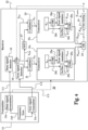
- Fig. 3 schematically illustrates a sparse data communication system 10 according to some possible embodiments, comprising a transmitter (Tx) 11 and a receiver (Rx) 12 configured to communicate over two separate communication channels, C1 and C2 (e.g., optical, RF, or electrical).
- the transmission on both communication channels is from the transmitter 11 to the receiver 12.
- the communication channel (data line) C1 is used to transmit serial sparse data signals (e . g ., single-photon quantum communication), and the communication channel C2 (synchronization line) is used to transmit serial synchronization signals (e.g., clock signals transmitted over a conventional data communication channel ( e.g., opticl fiber, electric cables, RF).
- serial synchronization signals e.g., clock signals transmitted over a conventional data communication channel (e.g., opticl fiber, electric cables, RF).
- the two communication channels, C1 and C2 are synchronized at the transmitter 11 by synchronization signals generated by its internal frequency synchronization circuitry (e.g., clock signal generator) 11f.
- the serial synchronization signals produced by the frequency synchronization circuitry 11f comprises a PRBS clock operating in in an infinite loop.
- the transmitter comprises a data signal transmitter 11t configured to transmit data signals over the sparse data communication channel C1, and a synchronization signal transmitter configured to transmit the synchronization signals generated by the frequency synchronization circuitry 11f over the synchronization signals communication channel C2.
- the distance between the transmitter 11 and the receiver 12 is not limited by the communication protocol disclosed herein.
- a data signal detector 13 is used to receive the serial data signals stream transmitted over the sparse data signals communication channel C1
- a synchronization signal detector 14 is used to receive the serial synchronization signals transmitted over the synchronization signals channel C2.
- the data and/or synchronization signals channels, C1 and/or C2 are optical channels, and in such embodiments the data signals detector 13 and the synchronization signals detector 14 are configured to convert the optical signals received over these channels into corresponding electrical signals.
- the synchronization signals channel C2 can be implemented by one or more optical fibers, and the serial synchronization signals transmitted thereover can be converted from optical to electrical signals S sync by an SFP module of the data signal detector 13.
- the synchronization signals comprise a PRBS having longer period and generated utilizing a predefined monic polynomial and seed value.
- the synchronization signals can comprise a known, balanced periodic digital clock signal, such as 01010101... (period of 2).
- the data channel C1 is a sparse single-photon quantum communication channel (e.g., implemented by optical fiber(s) or free space medium), and in such embodiments the data signal detector 13 can utilize optoelectronic measuring instruments, such as a single photon detector ( e . g ., avalanche photodiode), to convert the single-photon (qubits) signals transmitted thereover into corresponding electric signals S dat .
- the receiver 12 is required to determine the accurate timing of the data signals received therein over the sparse data signals communication channel C1.
- the electric synchronization signals S sync and the electric sparse data signals S dat are mixed together by a logical XOR gate circuit 15, which can be implemented by an external dedicated high speed circuit e.g., such as HMC745 manufactured by Analog Devices capable of operating with data rates of up to 13Gbps.
- a logical XOR gate circuit 15 can be implemented by an external dedicated high speed circuit e.g., such as HMC745 manufactured by Analog Devices capable of operating with data rates of up to 13Gbps.
- a tuneable delay unit TD can be used to align the data ( S dat ) and synchronization (S sync ) signals in time, for accurate bit signals overlap, as will be explained below.
- the tuneable delay unit TD is used for controllably affecting a delay to the serial data signal stream S dat , but in possible embodiments it can be similarly used to delay the synchronization signals S sync .
- the mixed signal S mix produced by the serial logical XOR gate circuit 15 is fed into the conventional transceiver device 16, for synchronization and processing.
- the frequency of the mixed signal S mix is recovered by the CDR circuitry 16c of the transceiver 16.
- the frequency recovered by the CDR circuitry 16c is used by the synchronization signal emulator 16e to generate local synchronization signals for the components of the transceiver device 16. Accordingly, if the synchronization signals source 11f of the transmitter comprises PRBS signals, the synchronization signal emulator 16e is configured to generate PRBS signals having the same frequency and periodicity, monic polynomial and seed value, of the PRBS signals used at the transmitter 11.
- a frame counter (not shown) can be used in some embodiments to count the bits since the beginning of the transmission.
- the frame counter can be configured to count the number of frames, which comprises 64bit words of a PRBS clock of the synchronization signal emulator 16e.
- a PRBS loop counter having an odd length is implemented in the synchronization signal emulator 16e by a 64bits PRBS clock generator e.g., a PRBS7 having a 127bits length, so every 64bit word (loop) is not a whole PRBS loop and may contain bits from more than one PRBS loops which are counted by the frame counter.
- An internal parallel logical XOR gate circuit 16x of the transceiver device 16 can be used to demix the lower rate parallel (deserialized) mixed signals stream P mix with the lower rate parallel (deserialized) synchronization signals E sync , and thereby remove the redundancy introduced into the serial data signal stream S dat by the serial logical XOR gate circuit 15.
- the fine tuning module 19 can be similarly used to accurately register the lower rate parallel data stream P dat produced by the internal parallel logical XOR gate circuit 16x with respect to the synchronization signals of the transmitter 11, by correlating at least a portion of the lower rate parallel data signals stream P dat with the predefined/known data pattern C pattern , as described hereinabove.
- Fig. 4 schematically illustrates a sparse data communication system 20 according to other possible embodiments.
- Some of the components of communication system 20 are similar to those of the communication system 10 of Fig. 3 , and thus designated by the same reference numerals.
- the main differences between the communication systems 10 and 20 is in the mixing and demixing of the data and synchronization signals, and in using two separate transceiver devices/channels at the receiver 22 for the synchronization and processing.
- the mixing performed at the receiver 22 utilizes first and second analog combiner circuitries, 21 and 23, each configured to perform a logical OR operation to electrical signals thereby received for adding reversible redundancy to the sparse data signal S dat .
- the first combiner 21 is configured to combine the synchronization signals S sync from the synchronization signal detector 14 with the sparse data signals S dat from the data signal detector 13, and the second combiner 23 is configured to combine the synchronization signals S sync inversed by the analog NOT/inversion circuitry 27 with the sparse data signals S dat .
- the combined signals, S c1 and S c2 , produced by the first and second combiners, 21 and 23, are fed into respective first and second transceiver devices/channels, 16 1 and 16 2 , for synchronization and processing.
- the demixed lower rate parallel data signals streams, P dmx1 and P dmx2 are combined by a parallel logical OR gate circuitry 24 to thereby produce the lower rate parallel data stream P dat from which the redundancy added by the analog combiner circuitries, 21 and 23, to the sparse data signals S dat is removed.
- the fine tuning module 19 can be similarly used to accurately register the lower rate parallel data signals stream P dat produced by the parallel logical OR gate circuitry 24 by correlating at least a portion of the lower rate parallel data stream P dat with data pattern C pattern , which may be alternatively transmitted to the receiver 12 over the conventional/service channel C3, as described hereinabove.
- the timing data determined by the fine tuning module 19 can be used to set the delay time affected by the tuneable delay unit TD.
- Fig. 5 schematically illustrates a sparse data communication system 30 according to yet other possible embodiments.
- Some of the components of communication system 30 are similar to those of the communication system 20 of Fig. 4 , and thus designated by the same reference numerals.
- the main differences between the communication systems 20 and 30 is that the removal of the redundancy from receive data signal is carried out by a parallel logical AND circuitry 34 configured to operate on the lower rate parallel (deserialized) combined signals streams, P c1 and P c2 , produced by the SERDES circuitry, 25r and 26r of the transceiver devices, 16 1 ' and 16 2 '.
- the transceiver devices 16 1 ',16 2 ' therefore don't require the synchronization signal emulators 25e,26e and XOR circuitries 25x,26x of the transceiver devices 16 1 ,16 2 shown in Fig. 4 .
- the fine tuning module 19 can be similarly used to accurately register the lower rate parallel data signals stream P dat produced by the parallel logical AND gate circuitry 34 by correlating at least a portion of the lower rate parallel data signals stream P dat with predefined/ know data pattern C pattern , which may be alternatively transmitted to the receiver 12 over the conventional/service channel C3, as described hereinabove.
- the timing data determined by the fine tuning module 19 can be used to set the delay time affected by the tuneable delay unit TD.
- the use of PRBS in synchronization signals is advantageous over a 50% clock cycle signal ( i.e., having period of 2).
- the receiver device/channel 12 can be configured to identify how many bits are missing, and correct the timing of the received serial synchronization signals stream e . g. , based on the known monic polynomial and seed value of the PRBS.
- the SERDES mechanism can be configured to apply the required corrections.
- the transceiver devices/channels shown in Figs. 2 to 4 can be implemented by commercially available transceiver devices e.g., Intel (Altera) FPGAs such as Cyclone10, Arria10 and Stratix10.
- the transceiver(s) used in the disclosed embodiments comprises one or more processors (CPUs 16u) and memories (16m, shown in Fig. 2 ) configured and operable to carry out various procedures/functions and control schemes e . g ., signal processing and error analysis, fine tuning correlation.
- the CDR and SERDES functionalities of these transceivers can be exploited to recover the time and data of transmitted sparse data signals, per specific timing resolution and data rate of the transceiver selected for the implementation (e . g ., 25Gbps, allowing 40ps resolution).
- the inventors hereof tested the sparse data signals communication techniques disclosed herein utilizing remote transmitter-receiver setups with satisfactory results.
- Fig. 6 shows a flow diagram demonstrating a timing process 40 in the transmitter (Tx), the receiver (Rx), and between the transmitter and the receiver (Tx-Rx Comm.) in the sparse data communication systems according to possible embodiments.
- the sparse data communication system is synchronized, and continuously optimizes the accuracy of the synchronization signal emulation unit of the transceiver device(s)/channel(s).
- the receiver (Rx) waits for arrival of synchronization signals from the transmitter (Tx) over the synchronization signals channel (C2).
- the data signal detector (13) is disabled, to allow proper reception of a header of the synchronization, i.e. PRBS, signals.
- any predetermined signal patterns can be used for the header transmitted over the synchronization signals channel e.g., a sequence of 1,0,1,0,1,0,... having a predefined length.
- the transmitter (Tx) transmits the header signals over the synchronization signals channel (C2), followed by the synchronization signals (T2).
- the receiver (Rx) receives the header over the synchronization signals channel (C2), and thereafter activates the synchronization signal emulator (T3) (e.g., a local clock signal source, having the timing and periodicity (and polynomial and seed value if a PRBS is used) of the synchronization signals of the transmitter (Tx).
- T3 e.g., a local clock signal source, having the timing and periodicity (and polynomial and seed value if a PRBS is used
- the transmitter (Tx) can be configured to continuously transmit the synchronization signals (T4) over the synchronization signals channel (C2) for some predetermined time interval (e.g., 1us) required for the CDR circuitry of the receiver's transceiver to recover and lock to the frequency of the synchronization signals received over the synchronization signals channel (C2).
- some predetermined time interval e.g., 1us
- the timing information extracted from the time slots of the errors can be used to recover the sparse data received over the sparse data communication channel (C1), as these errors are introduced by the mixer (e.g., logical XOR gate) by mixing of the sparse data signals with the synchronization signals (e.g., PRBS).
- the mixer e.g., logical XOR gate
- the transmitter (Tx) introduces into the synchronization signals thereby transmitted a predefined (error) pattern (T7) that the transceiver(s) of the receiver (Rx) is configured to identify, for example, by flipping a predefined number of bits in the synchronization signals e . g ., flipping 1 bit every 128 bits of the synchronization signal, for 5 times.
- the transceiver(s) of the receiver (Rx) identifies the predefined (error) pattern introduced by the transmitter (Tx), it sets the tuneable delay (TD) unit (T8) to an initial delay thereby determined between the synchronization signals and the data signals, and activates (T9) the data signals receiver (13).
- the transmitter (Tx) then continuously transmits the synchronization and the data signals (T10), over the data signals channel ( C1 ) and the synchronization signals channel (C2), respectively.
- some of the data transmitted over the data signal channel ( C1 ) is known to receiver (Rx) e.g., a predefined pattern, or a data signal pattern communicated to the receiver over a different communication channel.
- the receiver (Rx) correlates (T10) the received data signals to the known/predefined data signal pattern, and based thereon accurately determines the delay time between the received synchronization and data signals (training), used for setting the tuneable delay (TD) unit.
- This training procedure can be carried out periodically, or intermittently, to compensate for drifts between the timing of the synchronization and data signals, and for maintaining the accurate delay time between the synchronization and data signals, so the synchronization between transmitter (Tx) and the receiver (Rx) is not lost.
- the receiver (Rx) can be configured to continuously identify time instances in which errors occurred in the demixed signals, and/or the synchronization signals, and/or electrical serial data signal stream (T12), and carry out necessary corrections based thereon. The corrected times can be used as the system output e.g., to another process/device.
- the delay time is calculated for blocks of sparse data signals, which is accurate only on average.
- Some of the parameters causing the delay time between the synchronization and data channels are physical, such as temperature of optical fibers and electronic components, which changes on a time scale of many seconds. If the variation of the delay is slow enough compared to the timescale of delay drift estimation, an interpolation and extrapolation of the delay time between measured time delays can be performed. This can be done both online, before outputting the recovered data signals, or offline, after data The recovered data is outputted. The simplest kind of interpolation and extrapolation is linear, but more sophisticated filters and estimators can be applied, depending on the drift pattern and mechanism.
- the mixing (e.g., by logical XOR gate circuitry) of data streams transmitted over two different communication channels with the same clock signal frequency is optimal when the phase (inter-bit delay) is optimal. This would make the timing resolution close to 1 bit (limited by the accuracy and jitter of other components of the system, such as the single photon detector). A phase of 1/2 bit will lower the resolution closer to 2 bits.
- the tuneable delay (TD) unit can be used in either the data or the synchronization channel (or both channels) to get a zero (0) phase between the synchronization and data signals channels.
- the communication systems disclosed herein can be configured to receive synchronization signals at the transmitter (Tx) and/or the receiver (Rx) from an external time synchronization system, as exemplified in Fig. 7 .
- the transmitter 11 is operated by an external synchronization system 71, operated in synchronization with an external synchronization system 72 that operates the receiver 12 (or 22).
- the synchronization between the external synchronization systems, 71 and 72 can be carried out over a conventional data communication channel C5.
- the receiver 12 (or 22) receives its synchronization signals over the conventional communication channel C2 from the external synchronization system 72
- the transmitter 11 receives its synchronization signals over the conventional communication channel C 24from the external synchronization system 71.
- a synchronized of 10.3Gbps clock can be recovered from user data e.g., CDR can be performed on optical signal taken form a tap to the optical channel used by other network users, located at both the transmitting and receiving sides, or from service channels, C4 and C2, provided at both the transmitting and receiving sides.
- this signal can be used as the input for a clock generating system (not shown), with the required clock, at both the transmitter 11 and the receiver 12/22, which gives the correct operation frequency to the participating parties.
- the receiver 12/22 can be configured to locally generate the required clock signal, i.e.
- the external synchronization system, 71 and 72 can be used to synchronize time counters provide in the transmitter 11 and the receiver 12/22, to record the time of events, where the transmission can have a different frequency.
- the delay time between transmitter 11 and the receiver 12/22 is initially found by correlation of the received sparse data signal to a predefined data signal pattern e.g., transmitted to the receiver over a conventional/service communication data channel.
- a communication channel with a known maximal latency can be used to indicate to the transmitter 11 to start transmitting data, and indicate to the receiver 12/22 to wait for incoming sparse data signals.
- the transmitter 11 starts transmitting the predefined data signal pattern used for the correlation.
- the delay between transmitter 11 and the receiver 12/22 is the time difference of optimal correlation. From this point the system will continue to periodically optimize the delay time.
- Fig. 7 further demonstrates use of a GPS clock for signaling the initial timing t0 for syncronization in sparse data communication according to possible embodiments.
- the sparse data communication techniques disclosed herein, with or without a dedicated synchronization signals communication channel, can be applied to one transmitter transmitting to any number of receivers, by splitting the synchronization and data signals, or by generating numerous synchronized synchronization and data signals. The process of setting the frequency, delay and phase would work independently for each receiver.
- the sparse data communication techniques disclosed herein can be utilized to communicate sparse data signal from multiple transmitters to a single receiver, by combining the sent sparse data signals before detection.
- the sparse data communication techniques utilizing the synchronization signals communication channel can be applied by sending and splitting the synchronization signal from the receiver to all transmitters, such that the transmitters receive the synchronization signals and locks the sparse data transmission signals to the received CDR. This will ensure that the frequency is the same for the receiver and all of the transmitters. Finding the delay time between the data and internal synchronization signals of the receiver can be done in the receiver, separately for each transmitter.
- the synchronization signals can be recovered as post process, without requiring the synchronization signals channel (C2), as exemplified in Fig. 8 .
- the frequency and delay time can be recovered in post process of the data using only the sparse data signals, using fitting to a model or to a polynom, for example.
- the synchronization signals channel comprises in some embodiments an optical channel, a dense wavelength division multiplexing (DWDM) channel for example, which normally transmits no data.
- DWDM dense wavelength division multiplexing
- data can be simply sent using circulators. Sending data in the direction of synchronization signals requires more effort.
- Data can be sent over this channel by flipping the synchronization signals bits (e.g., by XORing the data with the synchronization PRBS signals before serializing the synchronization signals and transmitting them). To have a clear separation between the received data signal (coming from detectors) and data sent over the synchronization signals channel, it is possible to calibrate the system for time sharing between signals coming from the sparse signals detector and signals coming from the synchronization signals channel.
- One possible method, applicable for short optical links (low latency links, usually below 1km) would be to use the detector dead time, which can be over 90% of the time.
- the receiver can inform the transmitter when no data is expected and data over the synchronization channel is allowed.
- Another possible method, which can work for any link length is as follows: After the receiver (Rx) estimates accurately the delay time between the data synchronization signals channels, it informs transmitter (Tx) which bits are signal free, and can be used to transmit data. The delay for the transmitter (Tx) is given relative to the known pattern (e.g., the 5 bit flips) sent before the beginning of the communication.
- ASICs application specific integrated circuits
- FPGAs field-programmable gated arrays
- the present invention provides communication techniques of sparse data signals and related methods. While particular embodiments of the invention have been described, it will be understood, however, that the invention is not limited thereto, since modifications may be made by those skilled in the art, particularly in light of the foregoing teachings. As will be appreciated by the skilled person, the invention can be carried out in a great variety of ways, employing more than one technique from those described above, all without exceeding the scope of the claims.
Landscapes
- Engineering & Computer Science (AREA)
- Computer Networks & Wireless Communication (AREA)
- Signal Processing (AREA)
- Physics & Mathematics (AREA)
- Electromagnetism (AREA)
- Computer Security & Cryptography (AREA)
- Optics & Photonics (AREA)
- Theoretical Computer Science (AREA)
- Optical Communication System (AREA)
- Synchronisation In Digital Transmission Systems (AREA)
- Mobile Radio Communication Systems (AREA)
- Communication Control (AREA)
- Time-Division Multiplex Systems (AREA)
Priority Applications (1)
| Application Number | Priority Date | Filing Date | Title |
|---|---|---|---|
| HRP20250422TT HRP20250422T1 (hr) | 2020-03-23 | 2021-03-22 | Sustav i postupak za sinkronizaciju i komunikaciju rijetkih podataka |
Applications Claiming Priority (2)
| Application Number | Priority Date | Filing Date | Title |
|---|---|---|---|
| US202062993097P | 2020-03-23 | 2020-03-23 | |
| PCT/IL2021/050322 WO2021191898A1 (en) | 2020-03-23 | 2021-03-22 | System and method for sparse data synchronization and communication |
Publications (3)
| Publication Number | Publication Date |
|---|---|
| EP4128650A1 EP4128650A1 (en) | 2023-02-08 |
| EP4128650B1 true EP4128650B1 (en) | 2025-02-26 |
| EP4128650C0 EP4128650C0 (en) | 2025-02-26 |
Family
ID=75478125
Family Applications (1)
| Application Number | Title | Priority Date | Filing Date |
|---|---|---|---|
| EP21718234.4A Active EP4128650B1 (en) | 2020-03-23 | 2021-03-22 | System and method for sparse data synchronization and communication |
Country Status (9)
| Country | Link |
|---|---|
| US (1) | US12278885B2 (pl) |
| EP (1) | EP4128650B1 (pl) |
| KR (1) | KR20250070035A (pl) |
| ES (1) | ES3014874T3 (pl) |
| HR (1) | HRP20250422T1 (pl) |
| HU (1) | HUE071808T2 (pl) |
| IL (2) | IL295736B2 (pl) |
| PL (1) | PL4128650T3 (pl) |
| WO (1) | WO2021191898A1 (pl) |
Families Citing this family (2)
| Publication number | Priority date | Publication date | Assignee | Title |
|---|---|---|---|---|
| US12348607B2 (en) * | 2022-06-30 | 2025-07-01 | Innophase, Inc. | Integrated circuit transceiver array synchronization |
| US12362799B2 (en) | 2022-06-30 | 2025-07-15 | Innophase, Inc. | Transceiver arrays for processing multi-resolution beam-formed data |
Citations (1)
| Publication number | Priority date | Publication date | Assignee | Title |
|---|---|---|---|---|
| WO2012105930A2 (en) * | 2010-01-29 | 2012-08-09 | Hewlett-Packard Development Company, L.P. | Quantum key distribution method and apparatus |
Family Cites Families (10)
| Publication number | Priority date | Publication date | Assignee | Title |
|---|---|---|---|---|
| WO2006039097A2 (en) | 2004-09-15 | 2006-04-13 | Magiq Technologies, Inc. | Dual-gated qkd system for wdm networks |
| JP2007288694A (ja) | 2006-04-19 | 2007-11-01 | Nec Corp | 秘匿通信システムおよびチャネル制御方法 |
| JP5550525B2 (ja) | 2010-10-29 | 2014-07-16 | ビアメカニクス株式会社 | ガルバノスキャナ及びレーザ加工機 |
| JP5751005B2 (ja) | 2011-05-18 | 2015-07-22 | コニカミノルタ株式会社 | 画像安定化制御システムおよび画像形成装置 |
| GB2491115B (en) | 2011-05-19 | 2013-08-14 | Toshiba Res Europ Ltd | Synchronisation of weak light pulse communication system |
| EP3018840B1 (en) | 2014-11-10 | 2019-10-02 | Université de Genève | Apparatus and method for QKD quantum communication channel continuous synchronization and alignment |
| CN114900882B (zh) | 2019-02-23 | 2025-05-06 | 华为技术有限公司 | 一种更新定时提前的方法、终端及网络设备 |
| CN110213040B (zh) | 2019-04-12 | 2020-07-31 | 北京邮电大学 | 一种量子密钥分发业务的服务质量控制方法及装置 |
| FR3115954B1 (fr) | 2020-10-29 | 2023-12-01 | Thales Sa | Procede de securisation de transmission de donnees satellitaires et systeme de transmission associe |
| US11671180B2 (en) * | 2021-04-28 | 2023-06-06 | Quantum Machines | System and method for communication between quantum controller modules |
-
2021
- 2021-03-22 ES ES21718234T patent/ES3014874T3/es active Active
- 2021-03-22 WO PCT/IL2021/050322 patent/WO2021191898A1/en not_active Ceased
- 2021-03-22 HR HRP20250422TT patent/HRP20250422T1/hr unknown
- 2021-03-22 HU HUE21718234A patent/HUE071808T2/hu unknown
- 2021-03-22 EP EP21718234.4A patent/EP4128650B1/en active Active
- 2021-03-22 PL PL21718234.4T patent/PL4128650T3/pl unknown
-
2022
- 2022-08-18 IL IL295736A patent/IL295736B2/en unknown
- 2022-09-20 US US17/948,721 patent/US12278885B2/en active Active
-
2023
- 2023-09-20 IL IL318769A patent/IL318769A/en unknown
- 2023-09-20 KR KR1020257004672A patent/KR20250070035A/ko active Pending
Patent Citations (1)
| Publication number | Priority date | Publication date | Assignee | Title |
|---|---|---|---|---|
| WO2012105930A2 (en) * | 2010-01-29 | 2012-08-09 | Hewlett-Packard Development Company, L.P. | Quantum key distribution method and apparatus |
Non-Patent Citations (6)
| Title |
|---|
| "QKD Ontology;Draft ETSI GS QKD 007", ETSI DRAFT; DRAFT ETSI GS QKD 007, EUROPEAN TELECOMMUNICATIONS STANDARDS INSTITUTE (ETSI), 650, ROUTE DES LUCIOLES ; F-06921 SOPHIA-ANTIPOLIS ; FRANCE, vol. ISG - QKD, no. V0.0.4, 2 July 2010 (2010-07-02), pages 1 - 34, XP014242272, [retrieved on 20100702] * |
| BENNETT CHARLES H ET AL: "An Update on Quantum Cryptography", SAT 2015 18TH INTERNATIONAL CONFERENCE, AUSTIN, TX, USA, SEPTEMBER 24-27, 2015; [LECTURE NOTES IN COMPUTER SCIENCE; LECT.NOTES COMPUTER], SPRINGER, BERLIN, HEIDELBERG, PAGE(S) 475 - 480, ISBN: 978-3-540-74549-5, XP047288194 * |
| BIENFANG J C ET AL: "Quantum key distribution with 1.25 Gbps clock synchronization", QUANTUM ELECTRONICS CONFERENCE, 2004. (IQEC). INTERNATIONAL SAN FRANCISCO, CA, USA MAY 16-21, 2004, PISCATAWAY, NJ, USA,IEEE, 16 May 2004 (2004-05-16), pages 1146 - 1147, XP010753029, ISBN: 978-1-55752-778-3 * |
| FEIHU XU ET AL: "Quantum cryptography with realistic devices", ARXIV.ORG, CORNELL UNIVERSITY LIBRARY, 201 OLIN LIBRARY CORNELL UNIVERSITY ITHACA, NY 14853, 21 March 2019 (2019-03-21), XP081156389 * |
| J. C. BIENFANG ET AL.: "Quantum key distribution with 1.25 Gbps clock synchronization", OPTICS EXPRESS, vol. 12, no. 9, 2011 * |
| WANG YING ET AL: "BIST for 2.5-Gb/s SerDes based on dynamic detection", COMPUTATIONAL PROBLEM-SOLVING (ICCP), 2011 INTERNATIONAL CONFERENCE ON, IEEE, 21 October 2011 (2011-10-21), pages 132 - 135, XP032027780, ISBN: 978-1-4577-0602-8, DOI: 10.1109/ICCPS.2011.6092211 * |
Also Published As
| Publication number | Publication date |
|---|---|
| IL295736B1 (en) | 2025-09-01 |
| HUE071808T2 (hu) | 2025-09-28 |
| IL318769A (en) | 2025-04-01 |
| KR20250070035A (ko) | 2025-05-20 |
| IL295736B2 (en) | 2026-01-01 |
| US20230026148A1 (en) | 2023-01-26 |
| PL4128650T3 (pl) | 2025-06-09 |
| EP4128650C0 (en) | 2025-02-26 |
| ES3014874T3 (en) | 2025-04-25 |
| US12278885B2 (en) | 2025-04-15 |
| EP4128650A1 (en) | 2023-02-08 |
| WO2021191898A1 (en) | 2021-09-30 |
| IL295736A (en) | 2022-10-01 |
| HRP20250422T1 (hr) | 2025-06-06 |
Similar Documents
| Publication | Publication Date | Title |
|---|---|---|
| EP3018840B1 (en) | Apparatus and method for QKD quantum communication channel continuous synchronization and alignment | |
| JP6732026B2 (ja) | 量子鍵配送システムにエントロピー源を追加するための装置および方法 | |
| US7231558B2 (en) | System and method for network error rate testing | |
| US8050373B2 (en) | Phase interpolator based transmission clock control | |
| CN108737074B (zh) | 一种信息同步方法和装置 | |
| US12278885B2 (en) | System and method for sparse data synchronization and communication | |
| US9966994B2 (en) | Apparatus and methods for burst mode clock and data recovery for high speed serial communication links | |
| US20150326391A1 (en) | Method and apparatus for generating and processing quantum signal in regular frame unit for quantum encryption key distribution | |
| CN215420318U (zh) | 一种用于量子密钥分发的时间同步系统 | |
| WO2004096802A2 (en) | ANTIBIOTIC TETRAHYDRO-β-CARBOLINE DERIVATIVES | |
| Honda et al. | General-purpose data streaming FPGA TDC synchronized by SerDes-based clock synchronization technique | |
| GB2439771A (en) | Clock controlled gating in quantum cryptography apparatus | |
| US20090103672A1 (en) | Transmission system, transmitter, receiver, and transmission method | |
| CN114282677B (zh) | 一种主控制设备、从控制设备及量子计算系统 | |
| WO2023187836A1 (en) | Methods and system for fast synchronization in long range quantum key distribution | |
| WO2009121421A1 (en) | Method and apparatus for transferring timing information between clock domains | |
| US8615063B2 (en) | Level transition determination circuit and method for using the same | |
| CN112385157B (zh) | 数据网络的用户设备 | |
| US20260052004A1 (en) | Quantum based system and method of multipoint communications | |
| CN117713982A (zh) | 提高空间激光通信时间同步精度的方法及系统 | |
| WO2024062482A1 (en) | Quantum based system and method of multipoint communications | |
| Calvet et al. | Development and Test of a 48-Optical Ports High-Precision Clock Distributor Board |
Legal Events
| Date | Code | Title | Description |
|---|---|---|---|
| STAA | Information on the status of an ep patent application or granted ep patent |
Free format text: STATUS: UNKNOWN |
|
| STAA | Information on the status of an ep patent application or granted ep patent |
Free format text: STATUS: THE INTERNATIONAL PUBLICATION HAS BEEN MADE |
|
| PUAI | Public reference made under article 153(3) epc to a published international application that has entered the european phase |
Free format text: ORIGINAL CODE: 0009012 |
|
| STAA | Information on the status of an ep patent application or granted ep patent |
Free format text: STATUS: REQUEST FOR EXAMINATION WAS MADE |
|
| 17P | Request for examination filed |
Effective date: 20221011 |
|
| AK | Designated contracting states |
Kind code of ref document: A1 Designated state(s): AL AT BE BG CH CY CZ DE DK EE ES FI FR GB GR HR HU IE IS IT LI LT LU LV MC MK MT NL NO PL PT RO RS SE SI SK SM TR |
|
| DAV | Request for validation of the european patent (deleted) | ||
| DAX | Request for extension of the european patent (deleted) | ||
| STAA | Information on the status of an ep patent application or granted ep patent |
Free format text: STATUS: EXAMINATION IS IN PROGRESS |
|
| 17Q | First examination report despatched |
Effective date: 20231102 |
|
| GRAP | Despatch of communication of intention to grant a patent |
Free format text: ORIGINAL CODE: EPIDOSNIGR1 |
|
| STAA | Information on the status of an ep patent application or granted ep patent |
Free format text: STATUS: GRANT OF PATENT IS INTENDED |
|
| INTG | Intention to grant announced |
Effective date: 20240925 |
|
| GRAS | Grant fee paid |
Free format text: ORIGINAL CODE: EPIDOSNIGR3 |
|
| GRAA | (expected) grant |
Free format text: ORIGINAL CODE: 0009210 |
|
| STAA | Information on the status of an ep patent application or granted ep patent |
Free format text: STATUS: THE PATENT HAS BEEN GRANTED |
|
| AK | Designated contracting states |
Kind code of ref document: B1 Designated state(s): AL AT BE BG CH CY CZ DE DK EE ES FI FR GB GR HR HU IE IS IT LI LT LU LV MC MK MT NL NO PL PT RO RS SE SI SK SM TR |
|
| RAP3 | Party data changed (applicant data changed or rights of an application transferred) |
Owner name: HEQA SECURITY LTD |
|
| REG | Reference to a national code |
Ref country code: GB Ref legal event code: FG4D |
|
| REG | Reference to a national code |
Ref country code: CH Ref legal event code: EP |
|
| REG | Reference to a national code |
Ref country code: DE Ref legal event code: R096 Ref document number: 602021026764 Country of ref document: DE |
|
| REG | Reference to a national code |
Ref country code: IE Ref legal event code: FG4D |
|
| PGFP | Annual fee paid to national office [announced via postgrant information from national office to epo] |
Ref country code: IE Payment date: 20250312 Year of fee payment: 5 |
|
| PGFP | Annual fee paid to national office [announced via postgrant information from national office to epo] |
Ref country code: NO Payment date: 20250312 Year of fee payment: 5 |
|
| PGFP | Annual fee paid to national office [announced via postgrant information from national office to epo] |
Ref country code: AT Payment date: 20250417 Year of fee payment: 5 |
|
| REG | Reference to a national code |
Ref country code: ES Ref legal event code: FG2A Ref document number: 3014874 Country of ref document: ES Kind code of ref document: T3 Effective date: 20250425 |
|
| PGFP | Annual fee paid to national office [announced via postgrant information from national office to epo] |
Ref country code: GB Payment date: 20250311 Year of fee payment: 5 |
|
| U01 | Request for unitary effect filed |
Effective date: 20250325 |
|
| U07 | Unitary effect registered |
Designated state(s): AT BE BG DE DK EE FI FR IT LT LU LV MT NL PT RO SE SI Effective date: 20250331 |
|
| U20 | Renewal fee for the european patent with unitary effect paid |
Year of fee payment: 5 Effective date: 20250410 |
|
| REG | Reference to a national code |
Ref country code: HR Ref legal event code: ODRP Ref document number: P20250422T Country of ref document: HR Payment date: 20250411 Year of fee payment: 5 |
|
| REG | Reference to a national code |
Ref country code: HR Ref legal event code: T1PR Ref document number: P20250422 Country of ref document: HR |
|
| PG25 | Lapsed in a contracting state [announced via postgrant information from national office to epo] |
Ref country code: RS Free format text: LAPSE BECAUSE OF FAILURE TO SUBMIT A TRANSLATION OF THE DESCRIPTION OR TO PAY THE FEE WITHIN THE PRESCRIBED TIME-LIMIT Effective date: 20250526 |
|
| PGFP | Annual fee paid to national office [announced via postgrant information from national office to epo] |
Ref country code: PL Payment date: 20250312 Year of fee payment: 5 |
|
| PGFP | Annual fee paid to national office [announced via postgrant information from national office to epo] |
Ref country code: ES Payment date: 20250401 Year of fee payment: 5 |
|
| PG25 | Lapsed in a contracting state [announced via postgrant information from national office to epo] |
Ref country code: IS Free format text: LAPSE BECAUSE OF FAILURE TO SUBMIT A TRANSLATION OF THE DESCRIPTION OR TO PAY THE FEE WITHIN THE PRESCRIBED TIME-LIMIT Effective date: 20250626 |
|
| PGFP | Annual fee paid to national office [announced via postgrant information from national office to epo] |
Ref country code: HR Payment date: 20250411 Year of fee payment: 5 |
|
| PG25 | Lapsed in a contracting state [announced via postgrant information from national office to epo] |
Ref country code: GR Free format text: LAPSE BECAUSE OF FAILURE TO SUBMIT A TRANSLATION OF THE DESCRIPTION OR TO PAY THE FEE WITHIN THE PRESCRIBED TIME-LIMIT Effective date: 20250527 |
|
| PGFP | Annual fee paid to national office [announced via postgrant information from national office to epo] |
Ref country code: CH Payment date: 20250401 Year of fee payment: 5 |
|
| PGFP | Annual fee paid to national office [announced via postgrant information from national office to epo] |
Ref country code: HU Payment date: 20250523 Year of fee payment: 5 |
|
| REG | Reference to a national code |
Ref country code: HU Ref legal event code: AG4A Ref document number: E071808 Country of ref document: HU |
|
| PG25 | Lapsed in a contracting state [announced via postgrant information from national office to epo] |
Ref country code: SM Free format text: LAPSE BECAUSE OF FAILURE TO SUBMIT A TRANSLATION OF THE DESCRIPTION OR TO PAY THE FEE WITHIN THE PRESCRIBED TIME-LIMIT Effective date: 20250226 |
|
| PG25 | Lapsed in a contracting state [announced via postgrant information from national office to epo] |
Ref country code: CZ Free format text: LAPSE BECAUSE OF FAILURE TO SUBMIT A TRANSLATION OF THE DESCRIPTION OR TO PAY THE FEE WITHIN THE PRESCRIBED TIME-LIMIT Effective date: 20250226 |
|
| PG25 | Lapsed in a contracting state [announced via postgrant information from national office to epo] |
Ref country code: SK Free format text: LAPSE BECAUSE OF FAILURE TO SUBMIT A TRANSLATION OF THE DESCRIPTION OR TO PAY THE FEE WITHIN THE PRESCRIBED TIME-LIMIT Effective date: 20250226 |
|
| PG25 | Lapsed in a contracting state [announced via postgrant information from national office to epo] |
Ref country code: MC Free format text: LAPSE BECAUSE OF FAILURE TO SUBMIT A TRANSLATION OF THE DESCRIPTION OR TO PAY THE FEE WITHIN THE PRESCRIBED TIME-LIMIT Effective date: 20250226 |
|
| PLBE | No opposition filed within time limit |
Free format text: ORIGINAL CODE: 0009261 |
|
| STAA | Information on the status of an ep patent application or granted ep patent |
Free format text: STATUS: NO OPPOSITION FILED WITHIN TIME LIMIT |
|
| 26N | No opposition filed |
Effective date: 20251127 |