EP4126754B1 - Mems-vorrichtung auf einem substrat mit rutheniumbasiertem kontaktoberflächenmaterial - Google Patents
Mems-vorrichtung auf einem substrat mit rutheniumbasiertem kontaktoberflächenmaterial Download PDFInfo
- Publication number
- EP4126754B1 EP4126754B1 EP21720603.6A EP21720603A EP4126754B1 EP 4126754 B1 EP4126754 B1 EP 4126754B1 EP 21720603 A EP21720603 A EP 21720603A EP 4126754 B1 EP4126754 B1 EP 4126754B1
- Authority
- EP
- European Patent Office
- Prior art keywords
- bonding
- substrate
- cap
- switch device
- wafer
- Prior art date
- Legal status (The legal status is an assumption and is not a legal conclusion. Google has not performed a legal analysis and makes no representation as to the accuracy of the status listed.)
- Active
Links
Images


Classifications
-
- H—ELECTRICITY
- H01—ELECTRIC ELEMENTS
- H01H—ELECTRIC SWITCHES; RELAYS; SELECTORS; EMERGENCY PROTECTIVE DEVICES
- H01H1/00—Contacts
- H01H1/02—Contacts characterised by the material thereof
- H01H1/021—Composite material
- H01H1/023—Composite material having a noble metal as the basic material
- H01H1/0237—Composite material having a noble metal as the basic material and containing oxides
-
- B—PERFORMING OPERATIONS; TRANSPORTING
- B81—MICROSTRUCTURAL TECHNOLOGY
- B81B—MICROSTRUCTURAL DEVICES OR SYSTEMS, e.g. MICROMECHANICAL DEVICES
- B81B7/00—Microstructural systems ; Auxiliary parts of microstructural devices or systems
- B81B7/0032—Packages or encapsulation
- B81B7/0035—Packages or encapsulation for maintaining a controlled atmosphere inside of the chamber containing the MEMS
- B81B7/0041—Packages or encapsulation for maintaining a controlled atmosphere inside of the chamber containing the MEMS maintaining a controlled atmosphere with techniques not provided for in B81B7/0038
-
- B—PERFORMING OPERATIONS; TRANSPORTING
- B81—MICROSTRUCTURAL TECHNOLOGY
- B81C—PROCESSES OR APPARATUS SPECIALLY ADAPTED FOR THE MANUFACTURE OR TREATMENT OF MICROSTRUCTURAL DEVICES OR SYSTEMS
- B81C1/00—Manufacture or treatment of devices or systems in or on a substrate
- B81C1/00015—Manufacture or treatment of devices or systems in or on a substrate for manufacturing microsystems
- B81C1/00261—Processes for packaging MEMS devices
- B81C1/00277—Processes for packaging MEMS devices for maintaining a controlled atmosphere inside of the cavity containing the MEMS
- B81C1/00293—Processes for packaging MEMS devices for maintaining a controlled atmosphere inside of the cavity containing the MEMS maintaining a controlled atmosphere with processes not provided for in B81C1/00285
-
- H—ELECTRICITY
- H01—ELECTRIC ELEMENTS
- H01H—ELECTRIC SWITCHES; RELAYS; SELECTORS; EMERGENCY PROTECTIVE DEVICES
- H01H49/00—Apparatus or processes specially adapted to the manufacture of relays or parts thereof
-
- H—ELECTRICITY
- H01—ELECTRIC ELEMENTS
- H01H—ELECTRIC SWITCHES; RELAYS; SELECTORS; EMERGENCY PROTECTIVE DEVICES
- H01H59/00—Electrostatic relays; Electro-adhesion relays
- H01H59/0009—Electrostatic relays; Electro-adhesion relays making use of micromechanics
-
- H—ELECTRICITY
- H10—SEMICONDUCTOR DEVICES; ELECTRIC SOLID-STATE DEVICES NOT OTHERWISE PROVIDED FOR
- H10P—GENERIC PROCESSES OR APPARATUS FOR THE MANUFACTURE OR TREATMENT OF DEVICES COVERED BY CLASS H10
- H10P95/00—Generic processes or apparatus for manufacture or treatments not covered by the other groups of this subclass
-
- B—PERFORMING OPERATIONS; TRANSPORTING
- B81—MICROSTRUCTURAL TECHNOLOGY
- B81B—MICROSTRUCTURAL DEVICES OR SYSTEMS, e.g. MICROMECHANICAL DEVICES
- B81B2201/00—Specific applications of microelectromechanical systems
- B81B2201/01—Switches
- B81B2201/012—Switches characterised by the shape
- B81B2201/014—Switches characterised by the shape having a cantilever fixed on one side connected to one or more dimples
-
- B—PERFORMING OPERATIONS; TRANSPORTING
- B81—MICROSTRUCTURAL TECHNOLOGY
- B81C—PROCESSES OR APPARATUS SPECIALLY ADAPTED FOR THE MANUFACTURE OR TREATMENT OF MICROSTRUCTURAL DEVICES OR SYSTEMS
- B81C1/00—Manufacture or treatment of devices or systems in or on a substrate
- B81C1/00015—Manufacture or treatment of devices or systems in or on a substrate for manufacturing microsystems
- B81C1/00134—Manufacture or treatment of devices or systems in or on a substrate for manufacturing microsystems comprising flexible or deformable structures
- B81C1/0015—Cantilevers
-
- B—PERFORMING OPERATIONS; TRANSPORTING
- B81—MICROSTRUCTURAL TECHNOLOGY
- B81C—PROCESSES OR APPARATUS SPECIALLY ADAPTED FOR THE MANUFACTURE OR TREATMENT OF MICROSTRUCTURAL DEVICES OR SYSTEMS
- B81C1/00—Manufacture or treatment of devices or systems in or on a substrate
- B81C1/00015—Manufacture or treatment of devices or systems in or on a substrate for manufacturing microsystems
- B81C1/00134—Manufacture or treatment of devices or systems in or on a substrate for manufacturing microsystems comprising flexible or deformable structures
- B81C1/00166—Electrodes
-
- B—PERFORMING OPERATIONS; TRANSPORTING
- B81—MICROSTRUCTURAL TECHNOLOGY
- B81C—PROCESSES OR APPARATUS SPECIALLY ADAPTED FOR THE MANUFACTURE OR TREATMENT OF MICROSTRUCTURAL DEVICES OR SYSTEMS
- B81C1/00—Manufacture or treatment of devices or systems in or on a substrate
- B81C1/00015—Manufacture or treatment of devices or systems in or on a substrate for manufacturing microsystems
- B81C1/00134—Manufacture or treatment of devices or systems in or on a substrate for manufacturing microsystems comprising flexible or deformable structures
- B81C1/00182—Arrangements of deformable or non-deformable structures, e.g. membrane and cavity for use in a transducer
-
- H—ELECTRICITY
- H01—ELECTRIC ELEMENTS
- H01H—ELECTRIC SWITCHES; RELAYS; SELECTORS; EMERGENCY PROTECTIVE DEVICES
- H01H1/00—Contacts
- H01H1/0036—Switches making use of microelectromechanical systems [MEMS]
- H01H2001/0052—Special contact materials used for MEMS
Definitions
- MEMS switches such as Micro-Electro-Mechanical System (MEMS) switches often require packages to protect the microscale features from environmental contaminants. These packages are typically either discrete or formed through wafer bonding processes. A MEMS switch may not operate reliably and consistently when exposed to uncontrolled operational environmental conditions. Moisture and contamination could cause either a lack of initial performance or an increase in early device failures. Accordingly, it is common practice to contain such devices within a protective package, which, at least to some extent, separates an internal device environment from an external environment. The processes associated with enclosing the devices within a protective package are critical to creating a reliable and long-lasting, hermetically sealed switch device.
- Patent document US 2012/0175715 A1 describes a MEMS switch hermetically sealed under vacuum in a cavity where the switch contacts are made from Ruthenium dioxide.
- a fabrication method according to the invention is described by claim 1.
- a switching apparatus also according to the invention is described by claim 11.
- Example embodiments herein describe a MEMS switch device that is built on a substrate with the stoichiometric rutile structure Ruthenium Dioxide (RuO 2 ) as the contact surface material.
- the MEMS switch device is hermetic sealed by a bonding process, e.g., thermal compression (TC) wafer bonding process, in an environment containing a minority oxygen (O 2 ) and other inert gas, e.g. argon (Ar) and/or nitrogen (N 2 ).
- the contact material may be Ru, or a stack of metals with Ru as the top and exposed contact material, or a Ru alloy.
- the example embodiments further describe a process flow directed to creating the RuO 2 (a conductive oxide) contact surfaces, which are formed at the pre-bonding, oxygen plasma ash cleaning process of the glass substrate.
- Energized oxygen ions generated by plasma effectively react with Ru atoms on the contact material top surfaces to create a high-quality thin layer RuO 2 that is generated during the plasma ash cleaning.
- the resulting RuO 2 contacts enable the MEMS switch device to maintain a low contact resistance value throughout billions of switch cycles.
- the example embodiments further describe several device enhancement techniques.
- One technique relates to encapsulating oxygen inside the cavity to mitigate organic contamination accumulation on contact surfaces, which improves fabrication yield and switch device longevity.
- Another enhancement technique is a pre-bonding oxygen thermal treatment to increase the thickness of the RuO 2 contact.
- Inert gas may be added to the sealed environment to further improve the switch's lifetime.
- a MEMS switch device may be built on a wafer based substrate, e.g., silicon, silicon dioxide (SiO 2 ), fused silica, silica glass, quartz, sodium-doped glass, borosilicate glass, sapphire, SOI, et al.
- the RuO 2 contact surface material may be created by oxygen plasma ash of the glass substrate, and the deposited Ru contact material, before the thermal compression (TC) bonding process.
- the typical expectation of oxygen plasma ash is to clean any organic residual material on the substrate, including contact surfaces.
- the clean stoichiometric oxidized contact surface leads to low and stable contact resistance. Additional treatment steps, such as introducing oxygen at pre-bonding temperature ramping phase or during a mechanical bonding phase, will further solidify and thicken RuO 2 contact layers.
- the substrate and the cap may each comprise an insulating material.
- the platinum-group metal may be ruthenium (Ru), and the oxidized layer of the platinum-group metal may be ruthenium dioxide (RuO 2 ).
- Constructing the ohmic MEMS switch device may further comprise forming the ohmic MEMS switch device on the substrate using a thin-film microfabrication process. Forming the oxidized layer of the platinum-group metal on the outer surface of each of the one or more contacts may comprise performing an oxygen plasma ash procedure on the ohmic MEMS switch device.
- the method may further comprise performing an oxygen plasma ash cleaning procedure on the ohmic MEMS switch device, after forming the oxidized layer of the platinum-group metal on the outer surface of the one or more contacts, to enhance the oxidized layer of the platinum-group metal on the outer surface of the one or more contacts.
- the bonding atmosphere may have a proportion of oxygen within a range of 0.05% to 30%.
- Bonding the cap to the substrate may further comprise subjecting the cap and the substrate to a bonding temperature, and pressing the cap and the substrate together with a bonding force, according to a profile that characterizes the bonding temperature and the bonding force with respect to time.
- the substrate may be one of a plurality of substrates on a first wafer
- the cap may be one of a plurality of caps on a second wafer.
- Bonding the cap to the substrate may further comprise subjecting the first wafer and the second wafer to a bonding temperature, and pressing the first wafer and the second wafer together with a bonding force, according to a profile that characterizes the bonding temperature and the bonding force with respect to time.
- the bonding atmosphere may further comprise one or both of (i) nitrogen (N 2 ) and (ii) a noble inert gas.
- the substrate and the cap may each comprise an insulating material.
- the platinum-group metal may be ruthenium (Ru), and the oxidized layer of the platinum-group metal may be ruthenium dioxide (RuO 2 ).
- the ohmic MEMS switch device may be formed on the substrate using a thin-film microfabrication process.
- the oxidized layer of the platinum-group metal on the outer surface of each of the one or more contacts may be formed using an oxygen plasma ash procedure on the ohmic MEMS switch device.
- the oxidized layer of the platinum-group metal may be enhanced using an oxygen plasma ash cleaning procedure on the ohmic MEMS switch device after forming the oxidized layer of the platinum-group metal on the outer surface of the one or more contacts.
- the cavity atmosphere within the sealed cavity may have a proportion of oxygen within a range of 0.05% to 30%.
- the cap and the substrate may be subjected to a bonding temperature, and the cap and the substrate may be pressed together with a bonding pressure, according to a profile that characterizes the bonding temperature and the bonding pressure with respect to time.
- the insulating substrate may be one of a plurality of insulating substrates on a first insulating wafer
- the insulating cap may be one of a plurality of insulating caps on a second insulating wafer.
- the first insulating wafer and the second insulating wafer may be subjected to a bonding temperature, and the first insulating wafer and the second insulating wafer may be pressed together with a bonding pressure, according to a profile that characterizes the bonding temperature and the bonding pressure with respect to time.
- the cavity atmosphere may further comprise one or both of (i) nitrogen (N 2 ) and (ii) a noble inert gas.
- Ru ruthenium dioxide
- RuO 2 ruthenium dioxide
- Ru contact with RuO 2 contact surface material other embodiments may utilize a contact comprising any platinum-group metal (e.g., Ru, Rh, Pd, Os, Ir, or Pt), and a corresponding oxide layer of the platinum-group metal.
- platinum-group metal e.g., Ru, Rh, Pd, Os, Ir, or Pt
- Ru will grow a native, self-inhibit oxide surface layer when it is exposed to an environment containing O 2 . If the oxidation temperature is over a certain threshold (in most literature reported at above 200°C), the stoichiometric Ruthenium Dioxide (RuO 2 ) layer will form instead of other types of Ru oxide (e.g., RuO, RuO 3 and RuO 4 ).
- the stoichiometric RuO 2 is a conductive oxide material with intrinsic resistivity of about 3.5 ⁇ 4.6 ⁇ 10 -5 ⁇ •cm. This value is greater than the Ru intrinsic resistivity of 6.71 ⁇ 7.16 ⁇ 10 -6 ⁇ •cm, but much lower than other forms of Ru oxide.
- RuO 2 Under room temperate and gas environment, the oxidation process of Ru on its surface is self-limited up to 10 ⁇ .
- the surface RuO 2 has a dense lattice structure that limits penetration of O 2 to form more RuO 2 underneath, resulting in other types of Ru oxide. It has been discovered that a non-stoichiometric RuO 2 dominated contact will have 5 to 10 times higher contact resistance as compared to stoichiometric RuO 2 , and this resistance increases over the time of switch operation, whereas stoichiometric RuO 2 exhibits a stable low contact resistance.
- RuO 2 Other approaches to form RuO 2 include oxygen plasma treatment, sputtering RuO 2 directly on surface in an Ar/O 2 mixed environment, Chemical Vapor Deposition(CVD), or Atomic Layer Deposition (ALD).
- CVD Chemical Vapor Deposition
- ALD Atomic Layer Deposition
- the sputtering approach can yield much thicker oxidation layer than other methods. For these reasons, MEMS switches may be fabricated with Ru as the contact material, rather than gold, silver, copper, aluminum, and other such highly conductive metals.
- MEMS switches are generally built on a semiconductor substrate (e.g., silicon), because MEMS fabrication historically originated from silicon CMOS processing technology. The majority of MEMS device manufacturing infrastructure is therefore based on the use of a silicon substrate. Accordingly, the expectation/prediction is that, going forward, commercialization of MEMS switch technology will be predominantly implemented on a silicon-based substrate. Only for special applications (e.g., microwave technology) are MEMS switch devices built on substrate other than silicon.
- a hard material such as Ru
- Au gold
- the hard material itself employed as a contact will not prevent the early failure in switch cycling operation, typically less than a few hundred million cycles. Failure mechanisms may include wear-out, micro-welding, surfacing roughening due to fracture, and organic/polymer contaminants accumulation on surface. Oxidization of the Ru contact surface, or the direct deposition of RuO 2 as contact material, may greatly improve MEMS switch thermomechanical performance, and reduce organic accumulation on the contact surfaces.
- MEMS switch devices are typically packaged in a sealed, clean environment, to guarantee the device performance over a long lifetime, which is a widely adopted approach in traditional mechanical switch and relay products to avoid moisture and contamination of the switch contacts.
- the example embodiments described herein present a MEMS ohmic contact switch that may be built on an insulating substrate, e.g., silicon dioxide, fused silica, silica glass, quartz, sodium-doped glass, and borosilicate glass, although other non-insulating substrate materials (e.g., silicon) may alternatively be used.
- fused silica may be chosen as the base substrate material due to its property of extremely low electrical loss. This property facilitates a switch device that has superior low insertion loss for RF and microwave applications, as well as excellent isolation for use as a high-power DC and/or RF or microwave switch.
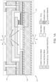
- FIG. 1A illustrates a detailed cross section of an example embodiment of a switch device 100 according to the invention.
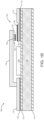
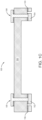
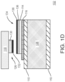
- FIGs. 1B , 1C and 1D illustrate detailed views of certain portions of the switch device depicted in FIG. 1A .
- the example switch device 100 comprises a substrate portion 104, shown in isolation in FIG. 1B , and a cap portion 106, which is shown in isolation in FIG. 1C .
- the contacts region 102 of the switch device 100 is shown in isolation and enlarged in FIG. 1D .
- the substrate portion 104 of the switch device 100 may comprise a substrate (e.g., fused silica) 108.
- An electrically-insulating material layer 110 may be deposited on one or both of the top surface and the bottom surface of the insulator substrate 108.
- Various metals and metal stacks can be used for either metal compression or metal eutectic bonding approaches. (metal stack can be for metal compression bonding or metal eutectic bonding).
- the bonding metal of the first and second bonding sites 112, 114 may be formed on an adhesion layer 116 deposited on the insulating material layer 110.
- the first and second bonding sites 114, 116 may bond with corresponding metal bonding sites on the cap portion 106 during the bonding procedure described herein.
- Such bonding defines a cavity 111a (see FIG. 1A ) around the switch elements (e.g., the beam, gate, and switching contacts, described herein) that isolates the switch elements from the environment 111b outside of the switch device 100.
- the environment within the cavity 111a can be different in pressure and gas composition than the environment 111b surrounding the bonded switch device.
- a first end of the beam 118 may be anchored to an electrically conductive trace that is in electrical communication to the bonding site 112 and mechanically coupled to the substrate 108.
- a first contact arrangement 126 may be disposed at a second end of the beam 118.
- the first contact arrangement 126 may comprise a Ru layer 130 mechanically coupled to the underside of and in electrical communication with the beam 118, and a RuO 2 layer 132 formed on the outer surface of the Ru layer 130.
- a second and corresponding contact arrangement 134 may comprise a Ru layer 136 deposited on an extension of a conductive trace that is in electrical communication to a bonding site (114) and mechanically adhered to the substrate 108, and a RuO 2 layer 138 formed on the outer surface of the Ru layer 136.
- the second contact 134 should be positioned below the beam and with similar X and Y coordinates as the first contact 126 such that when the beam is actuated by the gate electrode 140 and pulled toward the substrate the first and second contact surfaces touch and are in electrical communication. While in the example embodiment, the Ru layer 136 is deposited on the extension of the second bonding site 114, other embodiments may have the Ru layer deposited on a site other than a bonding site. For example, in some embodiments additional electrical circuit elements may be situated between the third contact arrangement 134 and the bonding site 114.
- a gate structure 140 may comprise a conductive metal layer 142 deposited on the insulator substrate 108.
- the gate structure 140 may be used to produce an electromotive force on the beam 118, which causes the beam to flex until the RuO 2 layer 132 of the first contact arrangement 126 is in electrical contact with the RuO 2 layer 138 of the second contact arrangement 134.
- the cap portion 106 of the switch device 100 may comprise an insulator cap 150, which comprises an insulating material such as fused silica or other such insulating material known in the art.
- a third bonding site 152 and a fourth bonding site 154, both comprising a bonding material such as, for example, gold (Au) may be formed on an adhesion layer 156 such as, for example, tantalum (Ta), deposited on the insulator cap 150, in positions conducive to bonding with the first bonding site 112 and the second bonding site 114.
- At least one conductive, hermetically sealed through-glass vias (TGV) 158 may be disposed in the insulator cap 150, which facilitates electrical signals being conducted to and/or from components of the switch device 100 that are sealed within the cavity formed after the cap portion 106 is bonded to the substrate portion 104.
- TSV through-glass vias
- the described embodiments employ an oxygen plasma ash process for two purposes prior to thermal compression (TC) bonding.
- the first purpose of the oxygen plasma ash process is to clean out organic contamination on contact surfaces.
- the second purpose of the oxygen plasma ash process is to deactivate the Ru contact surface to form RuO 2 .
- the subsequent bonding process is performed in an environment that contains a proportion of oxygen between 0.05% and 30%, although for the example embodiments, the oxygen proportion may not exceed 20%.
- the bonding environment may supplement the oxygen with one or more other gases, for example nitrogen (N 2 ), and/or a noble inert gas such as argon (Ar).
- the oxygen proportion of the gas sealed within the device environment may be at or near the oxygen proportion of the gas flow supplied during the bonding process.
- the proportion of oxygen in the sealed device environment may be 20%, although other environments may exhibit a proportion of oxygen between 0.05% and 30%.
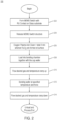
- FIG. 2 depicts an example embodiment of a process flow 200 for preparing and bonding a substrate wafer, which may host one or more MEMS switches, with a cap wafer.
- This example embodiment is directed to the use of a glass substrate wafer and a glass cap wafer, although other embodiments may utilize other insulating or non-insulating wafers. Further, it should be understood that any cap with suitable mating surfaces to facilitate bonding to the substrate portion in a wafer bonding process may be used.
- the process flow 200 may comprise forming 202 the device (e.g., the MEMS switch) on the glass substrate (e.g., the MEMS wafer), releasing 204 the MEMS switch structure (i.e., eliminating sacrificial support structures so that the switch components that are intended to be movable are free to move, thereby exposing the Ru contact surfaces), performing 206 an oxygen plasma ash clean procedure for at least 1 minute (4 minutes +/- 0.1 minute in an example embodiment),
- the MEMS wafer is bonded to a corresponding cap wafer to encapsulate the device and enable the hermetic sealing of the device within an oxygen containing environment.
- the cap wafer may be prepared through typical microfabrication processes to include any electrically functional or mechanical layers.
- the cap wafer contains materials and features to facilitate the bonding of the cap wafer to its corresponding MEMS device wafer, thus hermetically encapsulating the device.
- the substrate portion 104 and the cap portion 106 are aligned and loaded 208 into a thermal compression (TC) bonding chamber.
- TC thermal compression
- the process 200 continues by flowing 210 gas of a desired composition into the bonding chamber to a desired pressure, ramping up the chamber temperature, and bonding 212 the substrate and cap wafers at a specific temperature and force.
- the flow 214 of desired gas continues as the temperature is ramped down to conclude the example bonding process.
- gas is flowed 210 into the bond chamber to a desired pressure (described in more detail herein), a first bond force is applied (typically 20% or less of the subsequent second bond force) to contact the wafers (to one another), the temperature in the bonding chamber is ramped up, a second and higher force (bond force) is applied, thereby bonding 212 the cap portion 106 to the substrate portion 104.
- the bond chamber is maintained with the desired gas at its respective pressure, and the bond force is reduced to the first bond force (or similarly low force), and the temperature in the bonding chamber is ramped down.
- a conductive oxide contact surface (e.g., RuO 2 ) may be formed during the oxygen plasma ash process step 206, before MEMS wafers are loaded into thermal compression bonding equipment.
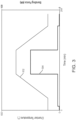
- An example TC profile is shown in FIG. 3 , with the chamber temperature 302 (in °C), shown along with the applied bonding force 304 (in kN). It should be understood that the temperatures and pressures depicted in FIG. 3 are examples presented for descriptive purposes only, and are not intended to be limiting. In general, the bonding temperature and pressure profile may fall within a range suitable for accomplishing the bond between the substrate and the cap as described herein.
- the gas used to fill the bonding chamber may be a N 2 /O 2 mixture, or clean dry air (CDA), or an inert gas/O 2 mixture, or just inert gas, or any gas just mentioned mixed with one or more noble inert gases.
- CDA clean dry air
- the stoichiometric rutile oxide, RuO 2 may be formed at the outer surface of the Ru contact. Highly reactive O 2 atoms may penetrate the surface of bulk Ru, but may form non-stoichiometric RuOx underneath the surface (where X is a positive real number). An anneal with O 2 will convert such RuOx to RuO 2 . As a result, additional optional steps after O 2 plasma ash and before the wafer bonding phase can yield thicker and higher percentage of RuO 2 as surface contact material. These options are demonstrated, for example, in FIGs. 5A, 5B, and 5C .
- FIG. 4A shows an example embodiment that comprises flowing 402 a gas containing oxygen (O 2 ) into the bonding chamber once the oxygen plasma ash steps are performed and the substrate and cap portions are loaded into the bonding chamber.
- FIG. 4B shows an example embodiment that comprises flowing 404 a gas containing nitrogen (N 2 ), in addition to oxygen, into the bonding chamber once the oxygen plasma ash steps are performed and the substrate and cap portions are loaded into the bonding chamber.
- FIG. 4C shows an example embodiment that comprises flowing 406 a gas containing a noble inert gas into the bonding chamber once the oxygen plasma ash steps are performed and the substrate and cap portions are loaded into the bonding chamber.
- the inert gas may be combined with O 2 , N 2 , or both.
- the final step shown concerns continuing the flow of gas described in steps 402, 404, and 406, respectively, as the bond between the substrate portion and the cap portion is formed.
- FIGs. 5A, 5B, and 5C show example embodiments that address pretreatment steps to form the RuO 2 contact layer described herein, prior to the bonding process.
- the RuO 2 layer is formed in a chamber (e.g., an oven) separate from the bonding chamber, rather than creating the RuO 2 layer during the oxygen plasma ash.
- the RuO 2 layer may be reinforced during the oxygen plasma ash.
- All three embodiments FIGs. 5A, 5B, and 5C ) show, after loading the MEMS device into an oven, filling 502 the oven with an oxygen-containing gas and annealing the device at greater than 200° C for at least 10 minutes.
- FIGs. 5A, 5B, and 5C show flowing oxygen 504, nitrogen 506, or a noble gas 508, respectively, in the bonding chamber.
Landscapes
- Engineering & Computer Science (AREA)
- Microelectronics & Electronic Packaging (AREA)
- Manufacturing & Machinery (AREA)
- Computer Hardware Design (AREA)
- Materials Engineering (AREA)
- Composite Materials (AREA)
- Chemical & Material Sciences (AREA)
- Micromachines (AREA)
- Physics & Mathematics (AREA)
- Condensed Matter Physics & Semiconductors (AREA)
- General Physics & Mathematics (AREA)
- Contacts (AREA)
- Manufacture Of Switches (AREA)
Claims (15)
- Verfahren zum Fertigen und Verkapseln einer ohmschen Mikroelektromechaniksystem(MEMS-)Schaltvorrichtung, das Folgendes umfasst:Aufbauen der ohmschen MEMS-Schaltvorrichtung auf einem Substrat, wobei die ohmsche MEMS-Schaltvorrichtung einen oder mehrere Kontakte aufweist, die aus einem Metall der Platingruppe bestehen,innerhalb einer ersten Kammer Formen einer oxidierten Schicht des Metalls der Platingruppe auf einer Außenfläche jedes von dem einen oder den mehreren Kontakten,innerhalb einer zweiten Kammer, die von der ersten Kammer getrennt ist, Binden einer Kappe an das Substrat, wodurch die ohmsche MEMS-Schaltvorrichtung innerhalb eines abgedichteten Hohlraums, der durch die Kappe und das Substrat gebildet wird, hermetisch versiegelt wird, wobei die Bindung in einer Bindungsatmosphäre erfolgt, die einen Anteil von Sauerstoff innerhalb eines Bereichs von 0,05 % bis 30 % aufweist, so dass, nachdem die ohmsche MEMS-Schaltvorrichtung innerhalb des abgedichteten Hohlraums hermetisch versiegelt worden ist, eine Hohlraumatmosphäre innerhalb des abgedichteten Hohlraums einen Anteil von Sauerstoff innerhalb des Bereichs von 0,05 % bis 30 % aufweist.
- Verfahren nach Anspruch 1, wobei das Substrat und die Kappe jeweils ein isolierendes Material aufweisen.
- Verfahren nach Anspruch 1, wobei das Metall der Platingruppe Ruthenium (Ru) ist und die oxidierte Schicht des Metalls der Platingruppe Rutheniumoxid (RuO2) ist.
- Verfahren nach Anspruch 1, wobei das Aufbauen der ohmschen MEMS-Schaltvorrichtung ferner das Formen der ohmschen MEMS-Schaltvorrichtung auf dem Substrat unter Verwendung eines Dünnschicht-Mikrofertigungsprozesses umfasst.
- Verfahren nach Anspruch 1, wobei das Formen der oxidierten Schicht des Metalls der Platingruppe auf der Außenfläche jedes von dem einen oder den mehreren Kontakten das Durchführen einer Sauerstoff-Plasmaveraschungsprozedur an der ohmschen MEMS-Schaltvorrichtung umfasst.
- Verfahren nach Anspruch 1, das ferner das Durchführen einer Sauerstoff-Plasmaveraschung-Reinigungsprozedur an der ohmschen MEMS-Schaltvorrichtung, nach dem Formen der oxidierten Schicht des Metalls der Platingruppe auf der Außenfläche des einen oder der mehreren Kontakte, umfasst, um die oxidierte Schicht des Metalls der Platingruppe auf der Außenfläche des einen oder der mehreren Kontakte zu verbessern.
- Verfahren nach Anspruch 1, wobei das Binden der Kappe an das Substrat ferner das Aussetzen der Kappe und des Substrats einer Bindungstemperatur und das Zusammenpressen der Kappe und des Substrats mit einer Bindungskraft, entsprechend einem Profil, das die Bindungstemperatur und die Bindungskraft in Bezug auf die Zeit kennzeichnet, umfasst.
- Verfahren nach Anspruch 1, wobei das Substrat eines von einer Vielzahl von Substraten auf einem ersten Wafer ist und die Kappe eine von einer Vielzahl von Kappen auf einem zweiten Wafer ist und das Binden der Kappe an das Substrat ferner das Aussetzen des ersten Wafers und des zweiten Wafers einer Bindungstemperatur und das Zusammenpressen des ersten Wafers und des zweiten Wafers mit einer Bindungskraft, entsprechend einem Profil, das die Bindungstemperatur und die Bindungskraft in Bezug auf die Zeit kennzeichnet, umfasst.
- Verfahren nach Anspruch 1, wobei die Bindungsatmosphäre ferner eines oder beide von (i) Stickstoff (N2) und (ii) einem inerten Edelgas umfasst.
- Verfahren nach Anspruch 2, wobei das Substrat und die Kappe jeweils Quarzglas umfassen.
- Schalteinrichtung, die Folgendes umfassteine ohmsche Mikroelektromechaniksystem(MEMS-)Schaltvorrichtung, die auf einem Substrat aufgebaut ist, wobei die ohmsche MEMS-Schaltvorrichtung einen oder mehrere Kontakte aufweist, die aus einem Metall der Platingruppe bestehen,eine Kappe, die auf dem Substrat angeordnet ist und an dasselbe gebunden ist, um einen hermetisch abgedichteten Hohlraum zu bilden, der die ohmsche MEMS-Schaltvorrichtung umschließt,gekennzeichnet durcheine Hohlraumatmosphäre innerhalb des abgedichteten Hohlraums, die einen Anteil von Sauerstoff innerhalb eines Bereichs von 0,05 % bis 30 % aufweist,und eine oxidierte Schicht des Metalls der Platingruppe, die auf einer Außenfläche jedes von dem einen oder den mehreren Kontakten geformt ist.
- Schalteinrichtung nach Anspruch 11, wobei das Substrat und die Kappe jeweils ein isolierendes Material umfassen.
- Schalteinrichtung nach Anspruch 11, wobei das Metall der Platingruppe Ruthenium (Ru) ist und die oxidierte Schicht des Metalls der Platingruppe Rutheniumoxid (RuO2) ist.
- Schalteinrichtung nach Anspruch 11, wobei die oxidierte Schicht des Metalls der Platingruppe unter Verwendung einer Sauerstoff-Plasmaveraschung-Reinigungsprozedur an der ohmschen MEMS-Schaltvorrichtung nach dem Formen der oxidierten Schicht des Metalls der Platingruppe auf der Außenfläche des einen oder der mehreren Kontakte verbessert wird.
- Schalteinrichtung nach Anspruch 11, wobei das isolierende Substrat eines von einer Vielzahl von isolierenden Substraten auf einem ersten isolierenden Wafer ist und die isolierende Kappe eine von einer Vielzahl von isolierenden Kappen auf einem zweiten isolierenden Wafer ist, und um die isolierende Kappe an das isolierende Substrat zu binden, der erste isolierende Wafer und der zweite isolierende Wafer einer Bindungstemperatur ausgesetzt werden und der erste isolierende Wafer und der zweite isolierende Wafer mit einer Bindungskraft zusammengepresst werden, entsprechend einem Profil, das die Bindungstemperatur und die Bindungskraft in Bezug auf die Zeit kennzeichnet.
Applications Claiming Priority (2)
| Application Number | Priority Date | Filing Date | Title |
|---|---|---|---|
| US16/832,408 US11501928B2 (en) | 2020-03-27 | 2020-03-27 | MEMS device built on substrate with ruthenium based contact surface material |
| PCT/US2021/024382 WO2021195512A1 (en) | 2020-03-27 | 2021-03-26 | Mems device built on substrate with ruthenium based contact surface material |
Publications (2)
| Publication Number | Publication Date |
|---|---|
| EP4126754A1 EP4126754A1 (de) | 2023-02-08 |
| EP4126754B1 true EP4126754B1 (de) | 2025-01-08 |
Family
ID=75625635
Family Applications (1)
| Application Number | Title | Priority Date | Filing Date |
|---|---|---|---|
| EP21720603.6A Active EP4126754B1 (de) | 2020-03-27 | 2021-03-26 | Mems-vorrichtung auf einem substrat mit rutheniumbasiertem kontaktoberflächenmaterial |
Country Status (6)
| Country | Link |
|---|---|
| US (2) | US11501928B2 (de) |
| EP (1) | EP4126754B1 (de) |
| JP (2) | JP2023519328A (de) |
| KR (1) | KR20220153601A (de) |
| CN (1) | CN115335317A (de) |
| WO (1) | WO2021195512A1 (de) |
Families Citing this family (3)
| Publication number | Priority date | Publication date | Assignee | Title |
|---|---|---|---|---|
| US11501928B2 (en) | 2020-03-27 | 2022-11-15 | Menlo Microsystems, Inc. | MEMS device built on substrate with ruthenium based contact surface material |
| US20240274387A1 (en) * | 2023-02-14 | 2024-08-15 | Texas Instruments Incorporated | Electromechanical switch |
| EP4487903B1 (de) * | 2023-07-07 | 2025-06-04 | Schott Ag | Hermetische umfassung mit glasdurchgängen und medizinisches implantat mit einer solchen hermetischen umfassung |
Family Cites Families (43)
| Publication number | Priority date | Publication date | Assignee | Title |
|---|---|---|---|---|
| US5479042A (en) | 1993-02-01 | 1995-12-26 | Brooktree Corporation | Micromachined relay and method of forming the relay |
| KR100467318B1 (ko) | 2002-06-04 | 2005-01-24 | 한국전자통신연구원 | 저항식 전자기계적 접촉을 이용하는 미세전자기계적 소자 |
| US7906359B2 (en) | 2002-12-03 | 2011-03-15 | Analog Devices, Inc. | Method of forming a surface micromachined MEMS device |
| US7064442B1 (en) | 2003-07-02 | 2006-06-20 | Analog Devices, Inc. | Integrated circuit package device |
| US7275424B2 (en) | 2003-09-08 | 2007-10-02 | Analog Devices, Inc. | Wafer level capped sensor |
| US7344982B2 (en) * | 2003-11-24 | 2008-03-18 | Arizona Board Of Regents, Acting For And On Behalf Of Arizona State University | System and method of selectively depositing Ruthenium films by digital chemical vapor deposition |
| US7034393B2 (en) | 2003-12-15 | 2006-04-25 | Analog Devices, Inc. | Semiconductor assembly with conductive rim and method of producing the same |
| US7608534B2 (en) | 2004-06-02 | 2009-10-27 | Analog Devices, Inc. | Interconnection of through-wafer vias using bridge structures |
| US7288940B2 (en) | 2004-12-06 | 2007-10-30 | Analog Devices, Inc. | Galvanically isolated signal conditioning system |
| US7504841B2 (en) | 2005-05-17 | 2009-03-17 | Analog Devices, Inc. | High-impedance attenuator |
| US7737810B2 (en) | 2005-07-08 | 2010-06-15 | Analog Devices, Inc. | MEMS switching device protection |
| US7968364B2 (en) | 2005-10-03 | 2011-06-28 | Analog Devices, Inc. | MEMS switch capping and passivation method |
| JP2009510707A (ja) | 2005-10-03 | 2009-03-12 | アナログ デバイシス, インコーポレイテッド | Memsスイッチ接点システム |
| JP2009540562A (ja) * | 2006-06-05 | 2009-11-19 | ダウ・コーニング・コーポレイション | 電子パッケージ及びその製造方法 |
| WO2008079887A2 (en) | 2006-12-21 | 2008-07-03 | Analog Devices, Inc. | Stacked mems device |
| KR101084447B1 (ko) | 2006-12-22 | 2011-11-21 | 아나로그 디바이시즈 인코포레이티드 | 스위치 구동 방법 및 장치 |
| US7612537B2 (en) | 2007-01-25 | 2009-11-03 | Analog Devices, Inc. | Galvanically isolated charge balance system |
| US8215151B2 (en) | 2008-06-26 | 2012-07-10 | Analog Devices, Inc. | MEMS stiction testing apparatus and method |
| US7928794B2 (en) | 2008-07-21 | 2011-04-19 | Analog Devices, Inc. | Method and apparatus for a dynamically self-bootstrapped switch |
| US8294539B2 (en) | 2008-12-18 | 2012-10-23 | Analog Devices, Inc. | Micro-electro-mechanical switch beam construction with minimized beam distortion and method for constructing |
| US8368490B2 (en) | 2008-12-18 | 2013-02-05 | Analog Devices, Inc. | Micro-electro-mechanical switch beam construction with minimized beam distortion and method for constructing |
| US9892879B2 (en) | 2011-01-11 | 2018-02-13 | Qorvo Us, Inc. | Encapsulated micro-electromechanical system switch and method of manufacturing the same |
| US9778039B2 (en) * | 2011-10-31 | 2017-10-03 | The Regents Of The University Of Michigan | Microsystem device and methods for fabricating the same |
| US8946879B2 (en) | 2012-07-27 | 2015-02-03 | Analog Devices, Inc. | Packages and methods for 3D integration including two stacked dies with a portion of one die extending into a hole of the other die |
| WO2014081503A1 (en) | 2012-11-20 | 2014-05-30 | Exxonmobil Upstream Research Company | Drill string stabilizer recovery improvement features |
| US10283582B2 (en) | 2013-02-25 | 2019-05-07 | Analog Devices Global | Microelectronic circuits and integrated circuits including a non-silicon substrate |
| US9911563B2 (en) | 2013-07-31 | 2018-03-06 | Analog Devices Global | MEMS switch device and method of fabrication |
| US9764946B2 (en) | 2013-10-24 | 2017-09-19 | Analog Devices, Inc. | MEMs device with outgassing shield |
| US9659717B2 (en) | 2014-02-18 | 2017-05-23 | Analog Devices Global | MEMS device with constant capacitance |
| US9748048B2 (en) | 2014-04-25 | 2017-08-29 | Analog Devices Global | MEMS switch |
| US9583294B2 (en) | 2014-04-25 | 2017-02-28 | Analog Devices Global | MEMS swtich with internal conductive path |
| US10033179B2 (en) | 2014-07-02 | 2018-07-24 | Analog Devices Global Unlimited Company | Method of and apparatus for protecting a switch, such as a MEMS switch, and to a MEMS switch including such a protection apparatus |
| US9604841B2 (en) | 2014-11-06 | 2017-03-28 | Analog Devices, Inc. | MEMS sensor cap with multiple isolated electrodes |
| US9975757B2 (en) * | 2015-06-03 | 2018-05-22 | Taiwan Semiconductor Manufacturing Co., Ltd. | Wafer Level Hermetic Seal Process for microelectromechanical systems (MEMS) devices |
| US9954263B2 (en) * | 2015-08-28 | 2018-04-24 | General Electric Company | Radio frequency micro-electromechanical systems having inverted microstrip transmission lines and method of making the same |
| US9758367B2 (en) | 2015-12-09 | 2017-09-12 | Analog Devices, Inc. | Metallizing MEMS devices |
| IL263274B2 (en) * | 2016-05-26 | 2023-10-01 | Berkeley Lights Inc | Covalently adapted surfaces, kits and methods for their production and uses |
| US10529518B2 (en) | 2016-09-19 | 2020-01-07 | Analog Devices Global | Protection schemes for MEMS switch devices |
| US10388468B2 (en) | 2016-11-18 | 2019-08-20 | Innovative Micro Technology | Contact material for MEMS devices |
| US10825628B2 (en) | 2017-07-17 | 2020-11-03 | Analog Devices Global Unlimited Company | Electromagnetically actuated microelectromechanical switch |
| US10848152B2 (en) | 2018-03-15 | 2020-11-24 | Analog Devices Global Unlimited Company | Optically isolated micromachined (MEMS) switches and related methods comprising a light transmitting adhesive layer between an optical receiver and a light source |
| US10843920B2 (en) | 2019-03-08 | 2020-11-24 | Analog Devices International Unlimited Company | Suspended microelectromechanical system (MEMS) devices |
| US11501928B2 (en) | 2020-03-27 | 2022-11-15 | Menlo Microsystems, Inc. | MEMS device built on substrate with ruthenium based contact surface material |
-
2020
- 2020-03-27 US US16/832,408 patent/US11501928B2/en active Active
-
2021
- 2021-03-26 CN CN202180024343.XA patent/CN115335317A/zh active Pending
- 2021-03-26 WO PCT/US2021/024382 patent/WO2021195512A1/en not_active Ceased
- 2021-03-26 JP JP2022558209A patent/JP2023519328A/ja active Pending
- 2021-03-26 KR KR1020227034112A patent/KR20220153601A/ko active Pending
- 2021-03-26 EP EP21720603.6A patent/EP4126754B1/de active Active
-
2022
- 2022-10-14 US US18/046,774 patent/US12148580B2/en active Active
-
2025
- 2025-12-11 JP JP2025245345A patent/JP2026041990A/ja active Pending
Also Published As
| Publication number | Publication date |
|---|---|
| US12148580B2 (en) | 2024-11-19 |
| CN115335317A (zh) | 2022-11-11 |
| JP2026041990A (ja) | 2026-03-10 |
| WO2021195512A1 (en) | 2021-09-30 |
| US11501928B2 (en) | 2022-11-15 |
| WO2021195512A9 (en) | 2021-10-28 |
| US20230064520A1 (en) | 2023-03-02 |
| JP2023519328A (ja) | 2023-05-10 |
| EP4126754A1 (de) | 2023-02-08 |
| US20210304973A1 (en) | 2021-09-30 |
| KR20220153601A (ko) | 2022-11-18 |
Similar Documents
| Publication | Publication Date | Title |
|---|---|---|
| US12148580B2 (en) | MEMS device built on substrate with ruthenium based contact surface material | |
| EP2467861B1 (de) | Mems-schalter abdeckung und passivierungsmethode | |
| US8592926B2 (en) | Substrate bonding with metal germanium silicon material | |
| EP2751022B1 (de) | Verankerung einer mems-vorrichtung | |
| JP2001158926A (ja) | 貴金属合金を含有する製品とその製造方法 | |
| US20120161255A1 (en) | Sealed mems cavity and method of forming same | |
| US20090200678A1 (en) | Device comprising multi-layered thin film having excellent adhesive strength and method for fabricating the same | |
| US10388468B2 (en) | Contact material for MEMS devices | |
| US8513043B2 (en) | Method for MEMS device fabrication and device formed | |
| KR100863388B1 (ko) | 전자 소자 및 그 제조방법 | |
| JP2008016452A (ja) | 接点材料、接点材料を含む装置及びその製造方法 | |
| US20070115082A1 (en) | MEMS Switch Contact System | |
| Imbert et al. | Wafer level metallic bonding: Voiding mechanisms in copper layers | |
| US20260015222A1 (en) | Two stage plating for reduced Ni and NiO layer formation | |
| EP3052429B1 (de) | Verfahren zur erzielung einer guten haftung zwischen einem dielektrischen und einem organischen material | |
| JPH05314846A (ja) | 接 点 | |
| CN121487890A (zh) | 利用导电阻挡层的玻璃通孔 | |
| CN112111706A (zh) | 表面镀有金属的陶瓷件及其镀金属方法 | |
| US20120194306A1 (en) | Preventing contact stiction in micro relays | |
| JPH11203997A (ja) | 真空バルブの製造方法 | |
| JP2010232566A (ja) | ダイヤモンド電極構造 |
Legal Events
| Date | Code | Title | Description |
|---|---|---|---|
| STAA | Information on the status of an ep patent application or granted ep patent |
Free format text: STATUS: UNKNOWN |
|
| STAA | Information on the status of an ep patent application or granted ep patent |
Free format text: STATUS: THE INTERNATIONAL PUBLICATION HAS BEEN MADE |
|
| PUAI | Public reference made under article 153(3) epc to a published international application that has entered the european phase |
Free format text: ORIGINAL CODE: 0009012 |
|
| STAA | Information on the status of an ep patent application or granted ep patent |
Free format text: STATUS: REQUEST FOR EXAMINATION WAS MADE |
|
| 17P | Request for examination filed |
Effective date: 20221013 |
|
| AK | Designated contracting states |
Kind code of ref document: A1 Designated state(s): AL AT BE BG CH CY CZ DE DK EE ES FI FR GB GR HR HU IE IS IT LI LT LU LV MC MK MT NL NO PL PT RO RS SE SI SK SM TR |
|
| DAV | Request for validation of the european patent (deleted) | ||
| DAX | Request for extension of the european patent (deleted) | ||
| GRAP | Despatch of communication of intention to grant a patent |
Free format text: ORIGINAL CODE: EPIDOSNIGR1 |
|
| STAA | Information on the status of an ep patent application or granted ep patent |
Free format text: STATUS: GRANT OF PATENT IS INTENDED |
|
| INTG | Intention to grant announced |
Effective date: 20240807 |
|
| GRAS | Grant fee paid |
Free format text: ORIGINAL CODE: EPIDOSNIGR3 |
|
| GRAA | (expected) grant |
Free format text: ORIGINAL CODE: 0009210 |
|
| STAA | Information on the status of an ep patent application or granted ep patent |
Free format text: STATUS: THE PATENT HAS BEEN GRANTED |
|
| AK | Designated contracting states |
Kind code of ref document: B1 Designated state(s): AL AT BE BG CH CY CZ DE DK EE ES FI FR GB GR HR HU IE IS IT LI LT LU LV MC MK MT NL NO PL PT RO RS SE SI SK SM TR |
|
| REG | Reference to a national code |
Ref country code: GB Ref legal event code: FG4D |
|
| REG | Reference to a national code |
Ref country code: CH Ref legal event code: EP |
|
| REG | Reference to a national code |
Ref country code: DE Ref legal event code: R096 Ref document number: 602021024661 Country of ref document: DE |
|
| REG | Reference to a national code |
Ref country code: IE Ref legal event code: FG4D |
|
| REG | Reference to a national code |
Ref country code: SE Ref legal event code: TRGR |
|
| PGFP | Annual fee paid to national office [announced via postgrant information from national office to epo] |
Ref country code: AT Payment date: 20250417 Year of fee payment: 5 |
|
| REG | Reference to a national code |
Ref country code: LT Ref legal event code: MG9D |
|
| REG | Reference to a national code |
Ref country code: NL Ref legal event code: MP Effective date: 20250108 |
|
| REG | Reference to a national code |
Ref country code: AT Ref legal event code: MK05 Ref document number: 1758226 Country of ref document: AT Kind code of ref document: T Effective date: 20250108 |
|
| PG25 | Lapsed in a contracting state [announced via postgrant information from national office to epo] |
Ref country code: NL Free format text: LAPSE BECAUSE OF FAILURE TO SUBMIT A TRANSLATION OF THE DESCRIPTION OR TO PAY THE FEE WITHIN THE PRESCRIBED TIME-LIMIT Effective date: 20250108 |
|
| PG25 | Lapsed in a contracting state [announced via postgrant information from national office to epo] |
Ref country code: RS Free format text: LAPSE BECAUSE OF FAILURE TO SUBMIT A TRANSLATION OF THE DESCRIPTION OR TO PAY THE FEE WITHIN THE PRESCRIBED TIME-LIMIT Effective date: 20250408 |
|
| PG25 | Lapsed in a contracting state [announced via postgrant information from national office to epo] |
Ref country code: FI Free format text: LAPSE BECAUSE OF FAILURE TO SUBMIT A TRANSLATION OF THE DESCRIPTION OR TO PAY THE FEE WITHIN THE PRESCRIBED TIME-LIMIT Effective date: 20250108 |
|
| PG25 | Lapsed in a contracting state [announced via postgrant information from national office to epo] |
Ref country code: PL Free format text: LAPSE BECAUSE OF FAILURE TO SUBMIT A TRANSLATION OF THE DESCRIPTION OR TO PAY THE FEE WITHIN THE PRESCRIBED TIME-LIMIT Effective date: 20250108 |
|
| PG25 | Lapsed in a contracting state [announced via postgrant information from national office to epo] |
Ref country code: ES Free format text: LAPSE BECAUSE OF FAILURE TO SUBMIT A TRANSLATION OF THE DESCRIPTION OR TO PAY THE FEE WITHIN THE PRESCRIBED TIME-LIMIT Effective date: 20250108 |
|
| PG25 | Lapsed in a contracting state [announced via postgrant information from national office to epo] |
Ref country code: IS Free format text: LAPSE BECAUSE OF FAILURE TO SUBMIT A TRANSLATION OF THE DESCRIPTION OR TO PAY THE FEE WITHIN THE PRESCRIBED TIME-LIMIT Effective date: 20250508 Ref country code: NO Free format text: LAPSE BECAUSE OF FAILURE TO SUBMIT A TRANSLATION OF THE DESCRIPTION OR TO PAY THE FEE WITHIN THE PRESCRIBED TIME-LIMIT Effective date: 20250408 |
|
| PG25 | Lapsed in a contracting state [announced via postgrant information from national office to epo] |
Ref country code: HR Free format text: LAPSE BECAUSE OF FAILURE TO SUBMIT A TRANSLATION OF THE DESCRIPTION OR TO PAY THE FEE WITHIN THE PRESCRIBED TIME-LIMIT Effective date: 20250108 |
|
| PG25 | Lapsed in a contracting state [announced via postgrant information from national office to epo] |
Ref country code: PT Free format text: LAPSE BECAUSE OF FAILURE TO SUBMIT A TRANSLATION OF THE DESCRIPTION OR TO PAY THE FEE WITHIN THE PRESCRIBED TIME-LIMIT Effective date: 20250508 Ref country code: LV Free format text: LAPSE BECAUSE OF FAILURE TO SUBMIT A TRANSLATION OF THE DESCRIPTION OR TO PAY THE FEE WITHIN THE PRESCRIBED TIME-LIMIT Effective date: 20250108 |
|
| PG25 | Lapsed in a contracting state [announced via postgrant information from national office to epo] |
Ref country code: BG Free format text: LAPSE BECAUSE OF FAILURE TO SUBMIT A TRANSLATION OF THE DESCRIPTION OR TO PAY THE FEE WITHIN THE PRESCRIBED TIME-LIMIT Effective date: 20250108 Ref country code: GR Free format text: LAPSE BECAUSE OF FAILURE TO SUBMIT A TRANSLATION OF THE DESCRIPTION OR TO PAY THE FEE WITHIN THE PRESCRIBED TIME-LIMIT Effective date: 20250409 |
|
| PG25 | Lapsed in a contracting state [announced via postgrant information from national office to epo] |
Ref country code: AT Free format text: LAPSE BECAUSE OF FAILURE TO SUBMIT A TRANSLATION OF THE DESCRIPTION OR TO PAY THE FEE WITHIN THE PRESCRIBED TIME-LIMIT Effective date: 20250108 |
|
| PG25 | Lapsed in a contracting state [announced via postgrant information from national office to epo] |
Ref country code: SM Free format text: LAPSE BECAUSE OF FAILURE TO SUBMIT A TRANSLATION OF THE DESCRIPTION OR TO PAY THE FEE WITHIN THE PRESCRIBED TIME-LIMIT Effective date: 20250108 |
|
| REG | Reference to a national code |
Ref country code: DE Ref legal event code: R097 Ref document number: 602021024661 Country of ref document: DE |
|
| PG25 | Lapsed in a contracting state [announced via postgrant information from national office to epo] |
Ref country code: DK Free format text: LAPSE BECAUSE OF FAILURE TO SUBMIT A TRANSLATION OF THE DESCRIPTION OR TO PAY THE FEE WITHIN THE PRESCRIBED TIME-LIMIT Effective date: 20250108 |
|
| PG25 | Lapsed in a contracting state [announced via postgrant information from national office to epo] |
Ref country code: MC Free format text: LAPSE BECAUSE OF FAILURE TO SUBMIT A TRANSLATION OF THE DESCRIPTION OR TO PAY THE FEE WITHIN THE PRESCRIBED TIME-LIMIT Effective date: 20250108 |
|
| PG25 | Lapsed in a contracting state [announced via postgrant information from national office to epo] |
Ref country code: EE Free format text: LAPSE BECAUSE OF FAILURE TO SUBMIT A TRANSLATION OF THE DESCRIPTION OR TO PAY THE FEE WITHIN THE PRESCRIBED TIME-LIMIT Effective date: 20250108 Ref country code: CZ Free format text: LAPSE BECAUSE OF FAILURE TO SUBMIT A TRANSLATION OF THE DESCRIPTION OR TO PAY THE FEE WITHIN THE PRESCRIBED TIME-LIMIT Effective date: 20250108 |
|
| REG | Reference to a national code |
Ref country code: CH Ref legal event code: H13 Free format text: ST27 STATUS EVENT CODE: U-0-0-H10-H13 (AS PROVIDED BY THE NATIONAL OFFICE) Effective date: 20251023 |
|
| PG25 | Lapsed in a contracting state [announced via postgrant information from national office to epo] |
Ref country code: RO Free format text: LAPSE BECAUSE OF FAILURE TO SUBMIT A TRANSLATION OF THE DESCRIPTION OR TO PAY THE FEE WITHIN THE PRESCRIBED TIME-LIMIT Effective date: 20250108 |
|
| PG25 | Lapsed in a contracting state [announced via postgrant information from national office to epo] |
Ref country code: SK Free format text: LAPSE BECAUSE OF FAILURE TO SUBMIT A TRANSLATION OF THE DESCRIPTION OR TO PAY THE FEE WITHIN THE PRESCRIBED TIME-LIMIT Effective date: 20250108 |
|
| PLBE | No opposition filed within time limit |
Free format text: ORIGINAL CODE: 0009261 |
|
| STAA | Information on the status of an ep patent application or granted ep patent |
Free format text: STATUS: NO OPPOSITION FILED WITHIN TIME LIMIT |
|
| PG25 | Lapsed in a contracting state [announced via postgrant information from national office to epo] |
Ref country code: LU Free format text: LAPSE BECAUSE OF NON-PAYMENT OF DUE FEES Effective date: 20250326 |
|
| REG | Reference to a national code |
Ref country code: BE Ref legal event code: MM Effective date: 20250331 |
|
| 26N | No opposition filed |
Effective date: 20251009 |
|
| PG25 | Lapsed in a contracting state [announced via postgrant information from national office to epo] |
Ref country code: BE Free format text: LAPSE BECAUSE OF NON-PAYMENT OF DUE FEES Effective date: 20250331 |
|
| PG25 | Lapsed in a contracting state [announced via postgrant information from national office to epo] |
Ref country code: CH Free format text: LAPSE BECAUSE OF NON-PAYMENT OF DUE FEES Effective date: 20250331 |
|
| PG25 | Lapsed in a contracting state [announced via postgrant information from national office to epo] |
Ref country code: IE Free format text: LAPSE BECAUSE OF NON-PAYMENT OF DUE FEES Effective date: 20250326 |
|
| PG25 | Lapsed in a contracting state [announced via postgrant information from national office to epo] |
Ref country code: IT Free format text: LAPSE BECAUSE OF FAILURE TO SUBMIT A TRANSLATION OF THE DESCRIPTION OR TO PAY THE FEE WITHIN THE PRESCRIBED TIME-LIMIT Effective date: 20250108 |
|
| PGFP | Annual fee paid to national office [announced via postgrant information from national office to epo] |
Ref country code: SE Payment date: 20260211 Year of fee payment: 6 |
|
| PGFP | Annual fee paid to national office [announced via postgrant information from national office to epo] |
Ref country code: GB Payment date: 20260209 Year of fee payment: 6 |
|
| PGFP | Annual fee paid to national office [announced via postgrant information from national office to epo] |
Ref country code: DE Payment date: 20260204 Year of fee payment: 6 |
|
| PGFP | Annual fee paid to national office [announced via postgrant information from national office to epo] |
Ref country code: FR Payment date: 20260209 Year of fee payment: 6 |