EP4123601A1 - Fingerabdruck-erfassungsvorrichtung und verfahren zum herstellen derselben - Google Patents
Fingerabdruck-erfassungsvorrichtung und verfahren zum herstellen derselben Download PDFInfo
- Publication number
- EP4123601A1 EP4123601A1 EP22185863.2A EP22185863A EP4123601A1 EP 4123601 A1 EP4123601 A1 EP 4123601A1 EP 22185863 A EP22185863 A EP 22185863A EP 4123601 A1 EP4123601 A1 EP 4123601A1
- Authority
- EP
- European Patent Office
- Prior art keywords
- substrate
- pads
- flexible substrate
- disposed
- strip electrodes
- Prior art date
- Legal status (The legal status is an assumption and is not a legal conclusion. Google has not performed a legal analysis and makes no representation as to the accuracy of the status listed.)
- Granted
Links
Images


Classifications
-
- G—PHYSICS
- G06—COMPUTING OR CALCULATING; COUNTING
- G06V—IMAGE OR VIDEO RECOGNITION OR UNDERSTANDING
- G06V40/00—Recognition of biometric, human-related or animal-related patterns in image or video data
- G06V40/10—Human or animal bodies, e.g. vehicle occupants or pedestrians; Body parts, e.g. hands
- G06V40/12—Fingerprints or palmprints
- G06V40/13—Sensors therefor
- G06V40/1306—Sensors therefor non-optical, e.g. ultrasonic or capacitive sensing
-
- G—PHYSICS
- G06—COMPUTING OR CALCULATING; COUNTING
- G06V—IMAGE OR VIDEO RECOGNITION OR UNDERSTANDING
- G06V40/00—Recognition of biometric, human-related or animal-related patterns in image or video data
- G06V40/10—Human or animal bodies, e.g. vehicle occupants or pedestrians; Body parts, e.g. hands
- G06V40/12—Fingerprints or palmprints
- G06V40/13—Sensors therefor
-
- G—PHYSICS
- G06—COMPUTING OR CALCULATING; COUNTING
- G06F—ELECTRIC DIGITAL DATA PROCESSING
- G06F1/00—Details not covered by groups G06F3/00 - G06F13/00 and G06F21/00
- G06F1/16—Constructional details or arrangements
- G06F1/1613—Constructional details or arrangements for portable computers
- G06F1/1633—Constructional details or arrangements of portable computers not specific to the type of enclosures covered by groups G06F1/1615 - G06F1/1626
- G06F1/1637—Details related to the display arrangement, including those related to the mounting of the display in the housing
- G06F1/1652—Details related to the display arrangement, including those related to the mounting of the display in the housing the display being flexible, e.g. mimicking a sheet of paper, or rollable
-
- G—PHYSICS
- G06—COMPUTING OR CALCULATING; COUNTING
- G06F—ELECTRIC DIGITAL DATA PROCESSING
- G06F1/00—Details not covered by groups G06F3/00 - G06F13/00 and G06F21/00
- G06F1/16—Constructional details or arrangements
- G06F1/1613—Constructional details or arrangements for portable computers
- G06F1/1633—Constructional details or arrangements of portable computers not specific to the type of enclosures covered by groups G06F1/1615 - G06F1/1626
- G06F1/1656—Details related to functional adaptations of the enclosure, e.g. to provide protection against EMI, shock, water, or to host detachable peripherals like a mouse or removable expansions units like PCMCIA cards, or to provide access to internal components for maintenance or to removable storage supports like CDs or DVDs, or to mechanically mount accessories
-
- G—PHYSICS
- G06—COMPUTING OR CALCULATING; COUNTING
- G06F—ELECTRIC DIGITAL DATA PROCESSING
- G06F3/00—Input arrangements for transferring data to be processed into a form capable of being handled by the computer; Output arrangements for transferring data from processing unit to output unit, e.g. interface arrangements
- G06F3/01—Input arrangements or combined input and output arrangements for interaction between user and computer
- G06F3/03—Arrangements for converting the position or the displacement of a member into a coded form
- G06F3/041—Digitisers, e.g. for touch screens or touch pads, characterised by the transducing means
- G06F3/0412—Digitisers structurally integrated in a display
-
- G—PHYSICS
- G06—COMPUTING OR CALCULATING; COUNTING
- G06F—ELECTRIC DIGITAL DATA PROCESSING
- G06F3/00—Input arrangements for transferring data to be processed into a form capable of being handled by the computer; Output arrangements for transferring data from processing unit to output unit, e.g. interface arrangements
- G06F3/01—Input arrangements or combined input and output arrangements for interaction between user and computer
- G06F3/03—Arrangements for converting the position or the displacement of a member into a coded form
- G06F3/041—Digitisers, e.g. for touch screens or touch pads, characterised by the transducing means
- G06F3/0416—Control or interface arrangements specially adapted for digitisers
- G06F3/04164—Connections between sensors and controllers, e.g. routing lines between electrodes and connection pads
-
- G—PHYSICS
- G06—COMPUTING OR CALCULATING; COUNTING
- G06F—ELECTRIC DIGITAL DATA PROCESSING
- G06F3/00—Input arrangements for transferring data to be processed into a form capable of being handled by the computer; Output arrangements for transferring data from processing unit to output unit, e.g. interface arrangements
- G06F3/01—Input arrangements or combined input and output arrangements for interaction between user and computer
- G06F3/03—Arrangements for converting the position or the displacement of a member into a coded form
- G06F3/041—Digitisers, e.g. for touch screens or touch pads, characterised by the transducing means
- G06F3/044—Digitisers, e.g. for touch screens or touch pads, characterised by the transducing means by capacitive means
- G06F3/0445—Digitisers, e.g. for touch screens or touch pads, characterised by the transducing means by capacitive means using two or more layers of sensing electrodes, e.g. using two layers of electrodes separated by a dielectric layer
-
- G—PHYSICS
- G06—COMPUTING OR CALCULATING; COUNTING
- G06F—ELECTRIC DIGITAL DATA PROCESSING
- G06F2203/00—Indexing scheme relating to G06F3/00 - G06F3/048
- G06F2203/041—Indexing scheme relating to G06F3/041 - G06F3/045
- G06F2203/04102—Flexible digitiser, i.e. constructional details for allowing the whole digitising part of a device to be flexed or rolled like a sheet of paper
-
- G—PHYSICS
- G06—COMPUTING OR CALCULATING; COUNTING
- G06F—ELECTRIC DIGITAL DATA PROCESSING
- G06F2203/00—Indexing scheme relating to G06F3/00 - G06F3/048
- G06F2203/041—Indexing scheme relating to G06F3/041 - G06F3/045
- G06F2203/04103—Manufacturing, i.e. details related to manufacturing processes specially suited for touch sensitive devices
Definitions
- the disclosure relates to a biometric sensing device, and more particularly to a fingerprint sensing device.
- a credit card has begun to incorporate fingerprint recognition functions.
- a conventional credit card with the fingerprint recognition function includes a main card and a secure chip disposed on the main card. Based on one or two sets of fingerprint data registered in a bank, when the conventional credit card with the fingerprint recognition function is placed on a card reader, and when the user's fingerprint is identified, the card reader can read the user's fingerprint data for a transaction.
- a credit card has to pass ISO7816 smart card standards, one of which is a flexibility test. Because the secure chip is made from a silicone material that has inflexible properties, it is difficult to pass the flexibility test. Further, when the conventional credit card with the fingerprint recognition function is received in a bag or pocket, the secure chip is easily damaged or broken due to folding or bending the conventional credit card with the fingerprint recognition function, thereby causing inconvenience in use. In addition, the process of silicone-based secure chips is limited by the existing semiconductor process and cannot be produced in batches, thereby limiting the production capacity of the secure chips.
- one object of the disclosure is to provide a fingerprint sensing device that can alleviate at least one of the drawbacks of the prior art.
- a fingerprint sensing device includes a flexible substrate unit, a sensing unit, and a chip unit.
- the flexible substrate unit includes a first flexible substrate, a double-sided flexible substrate, and a second flexible substrate which are stacked from top to bottom.
- the double-sided substrate has a first surface adjacent to the first flexible substrate, and a second surface adjacent to the second flexible substrate.
- the sensing unit includes a plurality of first strip electrodes, a plurality of second strip electrodes, a plurality of first electroconductive pads, a plurality of connecting pads, and a plurality of second electroconductive pads.
- the first strip electrodes are disposed on the first surface and are disposed between the first flexible substrate and the double-sided substrate.
- the second strip electrodes are disposed on the second surface and are disposed between the double-sided substrate and the second flexible substrate.
- the first electroconductive pads are disposed on a bottom surface of the first flexible substrate.
- the connecting pads and the second electroconductive pads are disposed on a top surface of the second flexible substrate.
- the first strip electrodes are upwardly connected to the first electroconductive pads.
- the first electroconductive pads are downwardly connected to the connecting pads.
- the second strip electrodes are downwardly connected to the second electroconductive pads.
- the chip unit is disposed on the second flexible substrate and is electrically connected to the connecting pads and the second electroconductive pads.
- Another object of the disclosure is to provide a method of making the fingerprint sensing device.
- a method of the disclosure includes
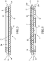
- FIG. 1 illustrate a fingerprint sensing device 1 according to a first embodiment of the disclosure.
- the fingerprint sensing device 1 includes a flexible substrate unit 2, a sensing unit 3, a chip unit 4, and an antistatic film 5.
- the flexible substrate unit 2 includes a first flexible substrate 21, a double-sided flexible substrate 22, and a second flexible substrate 23 which are stacked from top to bottom.
- the double-sided substrate 22 has a first surface 221 adjacent to the first flexible substrate 21, and a second surface 222 adjacent to the second flexible substrate 23.
- the first flexible substrate 21 has a window hole 20 and a plurality of first through holes 210 extending therethrough.
- the second flexible substrate 23 has a plurality of second through holes 230 extending therethrough.
- An area of the double-sided flexible substrate 22 is smaller than that of each of the first and second flexible substrate 21, 23.
- a thickness of each of the first flexible substrate 21, the double-sided flexible substrate 22, and the second flexible substrate 23 is greater than 0 ⁇ m and smaller than or equal to 50pm.
- the doubled-sided flexible substrate 22 has a length in the second direction (Y), which is smaller than a length of each of the first and second flexible substrates 21, 23 in the second direction (Y).
- a length of the doubled-sided flexible substrate 22 in the first direction (X) is smaller than that of each of the first and second flexible substrates 21, 23 in the first direction (X).
- the doubled-sided flexible substrate 22 further has two lateral sides that are opposite in the second direction (Y) and that respectively indent from two lateral sides of each of the first and second flexible substrates 21, 23 that are opposite in the second direction (Y), and other two lateral sides that are opposite in the first direction (X) and that respectively indent from the other two lateral sides of each of the first and second flexible substrates 21, 23 that are opposite in the first direction (X).
- Each of the first and second flexible substrates 21, 23 is made of, but not limited to, a material selected from a flexible printed circuit (fpc) board, a glass fiber (fr4) board, a bismaleimide-triazine (BT) resin, an ajinomoto build-up film (ABF), a molded interconnect substrate (MIS), a modified polyimide (MPI), and a liquid crystal polymer (LCP).
- the double-sided flexible substrate (22) is made of, but not limited to, a material selected from ultra-thin glass, polyimide (PI), polyethylene terephthalate (PET), modified polyimide (MPI), and liquid crystal polymer (LCP).
- the sensing unit 3 is a capacitive sensing unit and includes a plurality of first strip electrodes 31, a plurality of second strip electrodes 32, a plurality of first electroconductive pads 33, a plurality of connecting pads 34, and a plurality of second electroconductive pads 35.
- the first strip electrodes 31 are disposed on the first surface 221 and are disposed between the first flexible substrate 21 and the double-sided substrate 22.
- the second strip electrodes 32 are disposed on the second surface 222 and are disposed between the double-sided substrate 22 and the second flexible substrate 23.
- the first electroconductive pads 33 are disposed on a bottom surface of the first flexible substrate 21.
- the connecting pads 34 and the second electroconductive pads 35 are disposed on a top surface of the second flexible substrate 23.
- the first strip electrodes 31 disposed on the first surface 221 are spaced apart from each other in a first direction (X).
- Each of the first strip electrodes 31 has two first terminal portions 311 that are spaced apart from each other in a second direction (Y) and that are disposed on the first surface 221.
- the first terminal portions 311 of each of the strip electrodes 31 are respectively proximate to the lateral sides of the flexible double-sided substrate 22.
- the first electroconductive pads 33 disposed on the bottom surface of the first flexible substrate 21 are spaced apart from each other in the first direction (X), and respectively contact the first terminal portions 311 of the first strip electrodes 31.
- the connecting pads 34 disposed on the second flexible substrate 23 are spaced part from each other in a first direction X, and are upwardly and respectively connected to the first electroconductive pads 33.
- each first strip electrode 31 can be arranged to upwardly contact a part of the corresponding first electroconductive pad 33.
- the first electroconductive pads 33 are formed in pairs, and the first electroconductive pads 33 in each pair are respectively proximate to the lateral sides of the first flexible substrate 21.
- the connecting pads 34 are formed in pairs, and the connecting pads 34 in each pair are respectively proximate to the lateral sides of the second flexible substrate 23.
- Each of the first electroconductive pads 33 in each pair has an inner portion superimposed on and in contact with the corresponding first terminal portion 311, and an outer portion that extends outwardly beyond the flexible double-sided substrate 22 and that is superposed on and in contact with the corresponding connecting pad 34 disposed on the second flexible substrate 23.
- the second strip electrodes 32 disposed on the second surface 222 are spaced apart from each other in the second direction (Y).
- Each of the second strip electrodes 32 has two second terminal portions 321 that are spaced apart from each other in the first direction (X) and that are disposed on the second surface 222.
- the second electroconductive pads 35 disposed on the bottom surface of the second flexible substrate 23 are spaced apart from each other in the first direction (X), and the second strip electrodes 32 are downwardly connected to the second electroconductive pads 35.
- the second electroconductive pads 35 are respectively connected to the second terminal portions 321 of the second strip electrodes 32.
- the chip unit 4 is disposed on the second flexible substrate 23, and includes a drive chip 41 and a plurality of metal contacts 42.
- the drive chip 41 is disposed on a bottom surface of the second substrate 23, and is electrically connected to the connecting pads 34 and the second electroconductive pads 35 through a plurality of conducting wires (not shown).
- the metal contacts 42 are disposed on the bottom surface of the second substrate 23 and are electrically connected to the drive chip 41 through a plurality of conducting wires (not shown) . Since the connection of the connecting pads 34, the second electroconductive pads 35, and the chip unit 4 is well known in the art, the description thereof will not be repeated here in detail.
- the antistatic film 5 is formed in a looped shape and is disposed on a top surface of the first flexible substrate 21.
- the antistatic film 5 is electrically connected to the chip unit 4 by a plurality of conductors 51 extending through the first and second through holes 210, 230. Because the connection of the antistatic film 5 to the chip unit 4 is well known in art, the description thereof will not be repeated herein detail.
- Each of the first and second strip electrodes 31, 32, the first electroconductive pads 33, the connecting pads 34, the second electroconductive pads 35, and the metal contacts 42 is made of a material such as, but not limited to, gold, copper or aluminum.
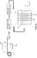
- the fingerprint sensing device 1 is combined with a credit card.
- the fingerprint sensing device 1 is first laid against a card reader and then is pressed by a finger.
- the sensing unit 3 through the change of the capacitance after being pressed, transmits an electrical signal incorporating a fingerprint information to the drive chip 41 and, through the metal contacts 42, to the card reader.
- the card reader cooperates with a database to compare the fingerprint information to complete the fingerprint authentication for an electronic transaction.
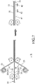
- Figures 6 to 8 illustrate a method of making a fingerprint sensing device of the disclosure.
- a first step is performed by providing a flexible and rollable double-sided substrate 22 having a first surface 221 and a second surface 222 opposite to the first surface 221, and laying metal layers 301, 302 respectively on the first and second surfaces 221, 222.
- the metal layers 301, 302 are laid respectively on the first and second surfaces 221, 222 by a method, such as evaporation, or sputtering, but not limited hereto.
- the material of the metal layers 301, 302 is, for example, but not limited to, gold, copper or aluminum.
- a subsequent step is performed by etching the metal layer 301 on the first surface 221 to form a plurality of spaced-apart first strip electrodes 31, and etching the metal layer 302 on the second surface 222 to form a plurality of spaced-apart second strip electrodes 32.
- the first strip electrodes 31 are spaced from each other in a first direction (X), and each first strip electrode 31 extends in a second direction (Y).
- the second strip electrodes 32 are spaced from each other in the second direction (Y), and each second strip electrode 32 extends in the first direction (X).
- the first and second directions (X, Y) are perpendicular to each other.
- each first strip electrode 31 is formed with two first terminal portions 311 spaced apart in a second direction (Y) on the first surface 221, and each second strip electrode 32 is formed with two second terminal portions 321 spaced apart in the first direction (X) on the second surface 222.
- Each of the metal layers 301, 302 is etched by, but not limited to, a wet or dry etching process.
- another subsequent step is performed by providing a flexible and rollable first substrate 21 that has an window hole 20, forming a plurality of first electroconductive pads 33 on a bottom surface of the first substrate 21, and bonding the bottom surface of the first substrate 21 to the first surface 221 of the double-sided substrate 22 in a roll-to-roll laminating manner so that the first electroconductive pads 33 are downwardly connected to the first strip electrodes 31.
- the first electroconductive pads 33 are formed in pairs on the bottom surface of the first substrate 21, the first electroconductive pads 33 in each pair are spaced in the second direction (Y), and the pairs of the first electroconductive pads 33 are spaced in the first direction (X). As such, the first electroconductive pads 33 respectively contact the first terminal portions 311 of the first strip electrodes 31.
- Still another subsequent step is performed by providing a flexible and rollable second substrate 23, forming a plurality of connecting pads 34 and a plurality of second electroconductive pads 35 on a top surface of the second substrate 23, and bonding the top surface of the second substrate 23 to the second surface 222 of the double-sided substrate 22 in a roll-to-roll laminating manner so that the connecting pads 34 are upwardly connected to the first electroconductive pads 33 and the second electroconductive pads 35 are upwardly connected to the second strip electrodes 32.
- the connecting pads 34 are formed in pairs on the top surface of the second substrate 23.
- the connecting pads 34 of each pair are spaced in the second direction (Y).
- the pairs of the connecting pads 34 are spaced in the first direction (X).
- the second electroconductive pads 35 are formed in pairs on the top surface of the second substrate 23.
- the second electroconductive pads 35 of each pair are spaced in the first direction (X).
- the pairs of the second electroconductive pads 35 are spaced in the second direction (Y).
- a chip unit 4 is placed on the second substrate 23, electrically connected to the connecting pads 34 and the second electroconductive pads 35, and is then packaged.
- the chip unit 4 includes a drive chip 41 disposed on a bottom surface of the second substrate 23 and a plurality of metal contacts 42 that are disposed on the bottom surface of the second substrate 23 and that are electrically connected to the drive chip 41.
- Still another step is performed by forming a plurality of first through holes 210 in the first substrate 21, forming a plurality of second through holes 230 in the second substrate 23, disposing an antistatic film 5 on a top surface of the first flexible substrate 21 in a roll-to-roll laminating manner, and providing a plurality of conductors 51 that extend through the first and second through holes 210, 230 and that electrically connect the antistatic film 5 and the chip unit 4.
- a trimming process is performed to form a plurality of individual fingerprint sensing devices 1.
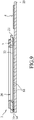
- Figure 9 illustrate a fingerprint sensing device 1 according to a second embodiment of the disclosure.
- the difference from the first embodiment resides in that the chip unit 4 in the second embodiment is disposed on the top surface of the second flexible substrate 23.
- the manufacturing steps for the second flexible substrate 23 can be concentrated on a same side thereof to meet different applications.
- the fingerprint sensing device 1 is flexible and is capable of passing the credit card flexibility test. Compared to the conventional sheet-to-sheet process, which requires clamping, the method of the disclosure making the fingerprint sensing device 1 is suitable for using the roll-to-roll techniques, and can reduce waste, significantly increase production capacity, and reduce the cost of production materials.
Landscapes
- Engineering & Computer Science (AREA)
- Theoretical Computer Science (AREA)
- General Engineering & Computer Science (AREA)
- General Physics & Mathematics (AREA)
- Physics & Mathematics (AREA)
- Human Computer Interaction (AREA)
- Computer Hardware Design (AREA)
- Multimedia (AREA)
- Computer Networks & Wireless Communication (AREA)
- Image Input (AREA)
- Measurement Of Length, Angles, Or The Like Using Electric Or Magnetic Means (AREA)
- Collating Specific Patterns (AREA)
- Measurement Of The Respiration, Hearing Ability, Form, And Blood Characteristics Of Living Organisms (AREA)
Applications Claiming Priority (1)
| Application Number | Priority Date | Filing Date | Title |
|---|---|---|---|
| TW110126999A TWI778719B (zh) | 2021-07-22 | 2021-07-22 | 指紋感測器及其製造方法 |
Publications (3)
| Publication Number | Publication Date |
|---|---|
| EP4123601A1 true EP4123601A1 (de) | 2023-01-25 |
| EP4123601C0 EP4123601C0 (de) | 2023-11-22 |
| EP4123601B1 EP4123601B1 (de) | 2023-11-22 |
Family
ID=82656717
Family Applications (1)
| Application Number | Title | Priority Date | Filing Date |
|---|---|---|---|
| EP22185863.2A Active EP4123601B1 (de) | 2021-07-22 | 2022-07-19 | Fingerabdruck-erfassungsvorrichtung und verfahren zum herstellen derselben |
Country Status (4)
| Country | Link |
|---|---|
| US (1) | US11756327B2 (de) |
| EP (1) | EP4123601B1 (de) |
| CN (1) | CN115690859A (de) |
| TW (1) | TWI778719B (de) |
Cited By (1)
| Publication number | Priority date | Publication date | Assignee | Title |
|---|---|---|---|---|
| US12131571B2 (en) * | 2022-08-10 | 2024-10-29 | Samsung Electronics Co., Ltd. | Fingerprint sensor package and smart card having the same |
Families Citing this family (1)
| Publication number | Priority date | Publication date | Assignee | Title |
|---|---|---|---|---|
| US20240212387A1 (en) * | 2022-12-23 | 2024-06-27 | Qualcomm Incorporated | Controlling rollable display devices based on fingerprint information and touch information |
Citations (5)
| Publication number | Priority date | Publication date | Assignee | Title |
|---|---|---|---|---|
| US20170053150A1 (en) * | 2015-08-17 | 2017-02-23 | Superc-Touch Corporation | Two-substrate fingerprint recognition device |
| US20170147852A1 (en) * | 2015-11-20 | 2017-05-25 | Idex Asa | Electronic sensor supported on rigid substrate |
| US20190087622A1 (en) * | 2017-09-19 | 2019-03-21 | Idex Asa | Double sided sensor module suitable for integration into electronic devices |
| US20190251322A1 (en) * | 2009-12-29 | 2019-08-15 | Idex Asa | Fingerprint sensor for incorporation into smartcard |
| US20200034594A1 (en) * | 2017-03-10 | 2020-01-30 | Fingerprint Cards Ab | Fingerprint sensor module comprising a fingerprint sensor device and a substrate connected to the sensor device |
Family Cites Families (9)
| Publication number | Priority date | Publication date | Assignee | Title |
|---|---|---|---|---|
| US5543589A (en) * | 1994-05-23 | 1996-08-06 | International Business Machines Corporation | Touchpad with dual sensor that simplifies scanning |
| US9274553B2 (en) * | 2009-10-30 | 2016-03-01 | Synaptics Incorporated | Fingerprint sensor and integratable electronic display |
| KR20120072793A (ko) * | 2010-12-24 | 2012-07-04 | 삼성전기주식회사 | 터치스크린 |
| TWI482263B (zh) * | 2013-05-20 | 2015-04-21 | 茂丞科技股份有限公司 | 發散式感測裝置及其製造方法 |
| WO2015026288A1 (en) * | 2013-08-23 | 2015-02-26 | Fingerprint Cards Ab | Connection pads for a fingerprint sensing device |
| US10394350B2 (en) * | 2014-08-11 | 2019-08-27 | Atmel Corporation | Fabricated electrical circuit on touch sensor substrate |
| US10325142B2 (en) * | 2015-04-23 | 2019-06-18 | Shenzhen GOODIX Technology Co., Ltd. | Multifunction fingerprint sensor |
| US11610429B2 (en) * | 2016-12-15 | 2023-03-21 | Fingerprint Cards Anacatum Ip Ab | Fingerprint sensing module and method for manufacturing the fingerprint sensing module |
| KR102509276B1 (ko) * | 2020-05-26 | 2023-03-13 | (주)파트론 | 광학식 지문 인식 센서 모듈 및 이를 적용한 전자 장치 |
-
2021
- 2021-07-22 TW TW110126999A patent/TWI778719B/zh active
-
2022
- 2022-04-27 CN CN202210448642.2A patent/CN115690859A/zh active Pending
- 2022-07-14 US US17/812,516 patent/US11756327B2/en active Active
- 2022-07-19 EP EP22185863.2A patent/EP4123601B1/de active Active
Patent Citations (5)
| Publication number | Priority date | Publication date | Assignee | Title |
|---|---|---|---|---|
| US20190251322A1 (en) * | 2009-12-29 | 2019-08-15 | Idex Asa | Fingerprint sensor for incorporation into smartcard |
| US20170053150A1 (en) * | 2015-08-17 | 2017-02-23 | Superc-Touch Corporation | Two-substrate fingerprint recognition device |
| US20170147852A1 (en) * | 2015-11-20 | 2017-05-25 | Idex Asa | Electronic sensor supported on rigid substrate |
| US20200034594A1 (en) * | 2017-03-10 | 2020-01-30 | Fingerprint Cards Ab | Fingerprint sensor module comprising a fingerprint sensor device and a substrate connected to the sensor device |
| US20190087622A1 (en) * | 2017-09-19 | 2019-03-21 | Idex Asa | Double sided sensor module suitable for integration into electronic devices |
Cited By (1)
| Publication number | Priority date | Publication date | Assignee | Title |
|---|---|---|---|---|
| US12131571B2 (en) * | 2022-08-10 | 2024-10-29 | Samsung Electronics Co., Ltd. | Fingerprint sensor package and smart card having the same |
Also Published As
| Publication number | Publication date |
|---|---|
| US11756327B2 (en) | 2023-09-12 |
| EP4123601C0 (de) | 2023-11-22 |
| CN115690859A (zh) | 2023-02-03 |
| TW202306447A (zh) | 2023-02-01 |
| EP4123601B1 (de) | 2023-11-22 |
| US20230027063A1 (en) | 2023-01-26 |
| TWI778719B (zh) | 2022-09-21 |
Similar Documents
| Publication | Publication Date | Title |
|---|---|---|
| TWI705384B (zh) | 適合集成於電子裝置的雙面感測器模組 | |
| CN105512715B (zh) | 芯片卡模块装置、芯片卡装置和用于制造芯片卡装置的方法 | |
| EP4123601B1 (de) | Fingerabdruck-erfassungsvorrichtung und verfahren zum herstellen derselben | |
| CN215495119U (zh) | 生物特征成像模块及智能卡 | |
| KR100846236B1 (ko) | 스마트 카드 웹 및 그 제조 방법 | |
| CN103942534B (zh) | 生物特征识别传感器及包含其的电子设备 | |
| KR20180038971A (ko) | 지문 센서 패키지 및 이를 포함하는 지문 센서 카드 및 지문 센서 모듈 | |
| KR20220013230A (ko) | 지문 센서 패키지 및 이를 포함하는 스마트 카드 | |
| CN108701248B (zh) | 集成电路卡的电路层 | |
| US11605237B1 (en) | Smart card fingerprint recognition module packaging structure and manufacturing method thereof | |
| CN205644554U (zh) | 指纹检测识别装置和具有其的电子设备 | |
| KR20220030214A (ko) | 직물에 스마트 카드를 연결하기 위한 장치 및 플렉시블 스마트 카드 형식의 전자 카드 제조 방법 | |
| US20240242054A1 (en) | Data-bearing card and semi-finished product and wiring layout for same, and method for producing same | |
| CN106356348A (zh) | 电容式传感器结构、具电容式传感器的电路板结构以及电容式传感器的封装结构 | |
| CN105205483A (zh) | 指纹感测装置 | |
| US12260278B2 (en) | Card-type medium and card-type medium manufacturing method | |
| US8724340B2 (en) | Data carrier for contactless data transmission and a method for producing such a data carrier | |
| US9811709B2 (en) | Capacitor sensor structure, circuit board structure with capacitor sensor, and package structure of capacitive sensor | |
| US11404361B2 (en) | Method for fabricating package structure having encapsulate sensing chip | |
| CN113206117A (zh) | 一种指纹识别封装结构及其制造方法 | |
| US20240202485A1 (en) | Wafer-level package sensor device | |
| TWM677396U (zh) | 具生物辨識功能之感應卡片 | |
| JPS60142489A (ja) | Icカ−ド | |
| CN117852569A (zh) | 智能卡片 | |
| KR20230056474A (ko) | 지문 센서 패키지 및 센서 패키지 |
Legal Events
| Date | Code | Title | Description |
|---|---|---|---|
| PUAI | Public reference made under article 153(3) epc to a published international application that has entered the european phase |
Free format text: ORIGINAL CODE: 0009012 |
|
| STAA | Information on the status of an ep patent application or granted ep patent |
Free format text: STATUS: THE APPLICATION HAS BEEN PUBLISHED |
|
| AK | Designated contracting states |
Kind code of ref document: A1 Designated state(s): AL AT BE BG CH CY CZ DE DK EE ES FI FR GB GR HR HU IE IS IT LI LT LU LV MC MK MT NL NO PL PT RO RS SE SI SK SM TR |
|
| STAA | Information on the status of an ep patent application or granted ep patent |
Free format text: STATUS: REQUEST FOR EXAMINATION WAS MADE |
|
| 17P | Request for examination filed |
Effective date: 20230303 |
|
| RBV | Designated contracting states (corrected) |
Designated state(s): AL AT BE BG CH CY CZ DE DK EE ES FI FR GB GR HR HU IE IS IT LI LT LU LV MC MK MT NL NO PL PT RO RS SE SI SK SM TR |
|
| GRAP | Despatch of communication of intention to grant a patent |
Free format text: ORIGINAL CODE: EPIDOSNIGR1 |
|
| STAA | Information on the status of an ep patent application or granted ep patent |
Free format text: STATUS: GRANT OF PATENT IS INTENDED |
|
| INTG | Intention to grant announced |
Effective date: 20230630 |
|
| GRAS | Grant fee paid |
Free format text: ORIGINAL CODE: EPIDOSNIGR3 |
|
| GRAA | (expected) grant |
Free format text: ORIGINAL CODE: 0009210 |
|
| STAA | Information on the status of an ep patent application or granted ep patent |
Free format text: STATUS: THE PATENT HAS BEEN GRANTED |
|
| AK | Designated contracting states |
Kind code of ref document: B1 Designated state(s): AL AT BE BG CH CY CZ DE DK EE ES FI FR GB GR HR HU IE IS IT LI LT LU LV MC MK MT NL NO PL PT RO RS SE SI SK SM TR |
|
| REG | Reference to a national code |
Ref country code: GB Ref legal event code: FG4D |
|
| REG | Reference to a national code |
Ref country code: CH Ref legal event code: EP |
|
| REG | Reference to a national code |
Ref country code: DE Ref legal event code: R096 Ref document number: 602022001088 Country of ref document: DE |
|
| REG | Reference to a national code |
Ref country code: IE Ref legal event code: FG4D |
|
| U01 | Request for unitary effect filed |
Effective date: 20231129 |
|
| U07 | Unitary effect registered |
Designated state(s): AT BE BG DE DK EE FI FR IT LT LU LV MT NL PT SE SI Effective date: 20231206 |
|
| PG25 | Lapsed in a contracting state [announced via postgrant information from national office to epo] |
Ref country code: GR Free format text: LAPSE BECAUSE OF FAILURE TO SUBMIT A TRANSLATION OF THE DESCRIPTION OR TO PAY THE FEE WITHIN THE PRESCRIBED TIME-LIMIT Effective date: 20240223 |
|
| PG25 | Lapsed in a contracting state [announced via postgrant information from national office to epo] |
Ref country code: IS Free format text: LAPSE BECAUSE OF FAILURE TO SUBMIT A TRANSLATION OF THE DESCRIPTION OR TO PAY THE FEE WITHIN THE PRESCRIBED TIME-LIMIT Effective date: 20240322 |
|
| PG25 | Lapsed in a contracting state [announced via postgrant information from national office to epo] |
Ref country code: ES Free format text: LAPSE BECAUSE OF FAILURE TO SUBMIT A TRANSLATION OF THE DESCRIPTION OR TO PAY THE FEE WITHIN THE PRESCRIBED TIME-LIMIT Effective date: 20231122 |
|
| PG25 | Lapsed in a contracting state [announced via postgrant information from national office to epo] |
Ref country code: IS Free format text: LAPSE BECAUSE OF FAILURE TO SUBMIT A TRANSLATION OF THE DESCRIPTION OR TO PAY THE FEE WITHIN THE PRESCRIBED TIME-LIMIT Effective date: 20240322 Ref country code: GR Free format text: LAPSE BECAUSE OF FAILURE TO SUBMIT A TRANSLATION OF THE DESCRIPTION OR TO PAY THE FEE WITHIN THE PRESCRIBED TIME-LIMIT Effective date: 20240223 Ref country code: ES Free format text: LAPSE BECAUSE OF FAILURE TO SUBMIT A TRANSLATION OF THE DESCRIPTION OR TO PAY THE FEE WITHIN THE PRESCRIBED TIME-LIMIT Effective date: 20231122 |
|
| PG25 | Lapsed in a contracting state [announced via postgrant information from national office to epo] |
Ref country code: RS Free format text: LAPSE BECAUSE OF FAILURE TO SUBMIT A TRANSLATION OF THE DESCRIPTION OR TO PAY THE FEE WITHIN THE PRESCRIBED TIME-LIMIT Effective date: 20231122 Ref country code: PL Free format text: LAPSE BECAUSE OF FAILURE TO SUBMIT A TRANSLATION OF THE DESCRIPTION OR TO PAY THE FEE WITHIN THE PRESCRIBED TIME-LIMIT Effective date: 20231122 Ref country code: HR Free format text: LAPSE BECAUSE OF FAILURE TO SUBMIT A TRANSLATION OF THE DESCRIPTION OR TO PAY THE FEE WITHIN THE PRESCRIBED TIME-LIMIT Effective date: 20231122 |
|
| PG25 | Lapsed in a contracting state [announced via postgrant information from national office to epo] |
Ref country code: CZ Free format text: LAPSE BECAUSE OF FAILURE TO SUBMIT A TRANSLATION OF THE DESCRIPTION OR TO PAY THE FEE WITHIN THE PRESCRIBED TIME-LIMIT Effective date: 20231122 |
|
| PG25 | Lapsed in a contracting state [announced via postgrant information from national office to epo] |
Ref country code: SK Free format text: LAPSE BECAUSE OF FAILURE TO SUBMIT A TRANSLATION OF THE DESCRIPTION OR TO PAY THE FEE WITHIN THE PRESCRIBED TIME-LIMIT Effective date: 20231122 |
|
| PG25 | Lapsed in a contracting state [announced via postgrant information from national office to epo] |
Ref country code: SM Free format text: LAPSE BECAUSE OF FAILURE TO SUBMIT A TRANSLATION OF THE DESCRIPTION OR TO PAY THE FEE WITHIN THE PRESCRIBED TIME-LIMIT Effective date: 20231122 Ref country code: SK Free format text: LAPSE BECAUSE OF FAILURE TO SUBMIT A TRANSLATION OF THE DESCRIPTION OR TO PAY THE FEE WITHIN THE PRESCRIBED TIME-LIMIT Effective date: 20231122 Ref country code: RO Free format text: LAPSE BECAUSE OF FAILURE TO SUBMIT A TRANSLATION OF THE DESCRIPTION OR TO PAY THE FEE WITHIN THE PRESCRIBED TIME-LIMIT Effective date: 20231122 Ref country code: CZ Free format text: LAPSE BECAUSE OF FAILURE TO SUBMIT A TRANSLATION OF THE DESCRIPTION OR TO PAY THE FEE WITHIN THE PRESCRIBED TIME-LIMIT Effective date: 20231122 |
|
| U20 | Renewal fee for the european patent with unitary effect paid |
Year of fee payment: 3 Effective date: 20240715 |
|
| REG | Reference to a national code |
Ref country code: DE Ref legal event code: R097 Ref document number: 602022001088 Country of ref document: DE |
|
| PLBE | No opposition filed within time limit |
Free format text: ORIGINAL CODE: 0009261 |
|
| STAA | Information on the status of an ep patent application or granted ep patent |
Free format text: STATUS: NO OPPOSITION FILED WITHIN TIME LIMIT |
|
| 26N | No opposition filed |
Effective date: 20240823 |
|
| PG25 | Lapsed in a contracting state [announced via postgrant information from national office to epo] |
Ref country code: MC Free format text: LAPSE BECAUSE OF FAILURE TO SUBMIT A TRANSLATION OF THE DESCRIPTION OR TO PAY THE FEE WITHIN THE PRESCRIBED TIME-LIMIT Effective date: 20231122 |
|
| PGFP | Annual fee paid to national office [announced via postgrant information from national office to epo] |
Ref country code: NO Payment date: 20250623 Year of fee payment: 4 |
|
| PG25 | Lapsed in a contracting state [announced via postgrant information from national office to epo] |
Ref country code: IE Free format text: LAPSE BECAUSE OF NON-PAYMENT OF DUE FEES Effective date: 20240719 |
|
| U20 | Renewal fee for the european patent with unitary effect paid |
Year of fee payment: 4 Effective date: 20250620 |
|
| PGFP | Annual fee paid to national office [announced via postgrant information from national office to epo] |
Ref country code: CH Payment date: 20250801 Year of fee payment: 4 |
|
| PG25 | Lapsed in a contracting state [announced via postgrant information from national office to epo] |
Ref country code: CY Free format text: LAPSE BECAUSE OF FAILURE TO SUBMIT A TRANSLATION OF THE DESCRIPTION OR TO PAY THE FEE WITHIN THE PRESCRIBED TIME-LIMIT; INVALID AB INITIO Effective date: 20220719 |