EP4120053A1 - Display device - Google Patents
Display device Download PDFInfo
- Publication number
- EP4120053A1 EP4120053A1 EP21767652.7A EP21767652A EP4120053A1 EP 4120053 A1 EP4120053 A1 EP 4120053A1 EP 21767652 A EP21767652 A EP 21767652A EP 4120053 A1 EP4120053 A1 EP 4120053A1
- Authority
- EP
- European Patent Office
- Prior art keywords
- region
- touch control
- display
- circuit board
- lines
- Prior art date
- Legal status (The legal status is an assumption and is not a legal conclusion. Google has not performed a legal analysis and makes no representation as to the accuracy of the status listed.)
- Granted
Links
Images





Classifications
-
- G—PHYSICS
- G06—COMPUTING OR CALCULATING; COUNTING
- G06F—ELECTRIC DIGITAL DATA PROCESSING
- G06F3/00—Input arrangements for transferring data to be processed into a form capable of being handled by the computer; Output arrangements for transferring data from processing unit to output unit, e.g. interface arrangements
- G06F3/01—Input arrangements or combined input and output arrangements for interaction between user and computer
- G06F3/03—Arrangements for converting the position or the displacement of a member into a coded form
- G06F3/041—Digitisers, e.g. for touch screens or touch pads, characterised by the transducing means
- G06F3/0416—Control or interface arrangements specially adapted for digitisers
- G06F3/04166—Details of scanning methods, e.g. sampling time, grouping of sub areas or time sharing with display driving
-
- H—ELECTRICITY
- H05—ELECTRIC TECHNIQUES NOT OTHERWISE PROVIDED FOR
- H05K—PRINTED CIRCUITS; CASINGS OR CONSTRUCTIONAL DETAILS OF ELECTRIC APPARATUS; MANUFACTURE OF ASSEMBLAGES OF ELECTRICAL COMPONENTS
- H05K1/00—Printed circuits
- H05K1/02—Details
- H05K1/14—Structural association of two or more printed circuits
- H05K1/147—Structural association of two or more printed circuits at least one of the printed circuits being bent or folded, e.g. by using a flexible printed circuit
-
- G—PHYSICS
- G02—OPTICS
- G02F—OPTICAL DEVICES OR ARRANGEMENTS FOR THE CONTROL OF LIGHT BY MODIFICATION OF THE OPTICAL PROPERTIES OF THE MEDIA OF THE ELEMENTS INVOLVED THEREIN; NON-LINEAR OPTICS; FREQUENCY-CHANGING OF LIGHT; OPTICAL LOGIC ELEMENTS; OPTICAL ANALOGUE/DIGITAL CONVERTERS
- G02F1/00—Devices or arrangements for the control of the intensity, colour, phase, polarisation or direction of light arriving from an independent light source, e.g. switching, gating or modulating; Non-linear optics
- G02F1/01—Devices or arrangements for the control of the intensity, colour, phase, polarisation or direction of light arriving from an independent light source, e.g. switching, gating or modulating; Non-linear optics for the control of the intensity, phase, polarisation or colour
- G02F1/13—Devices or arrangements for the control of the intensity, colour, phase, polarisation or direction of light arriving from an independent light source, e.g. switching, gating or modulating; Non-linear optics for the control of the intensity, phase, polarisation or colour based on liquid crystals, e.g. single liquid crystal display cells
- G02F1/133—Constructional arrangements; Operation of liquid crystal cells; Circuit arrangements
- G02F1/1333—Constructional arrangements; Manufacturing methods
- G02F1/13338—Input devices, e.g. touch panels
-
- G—PHYSICS
- G02—OPTICS
- G02F—OPTICAL DEVICES OR ARRANGEMENTS FOR THE CONTROL OF LIGHT BY MODIFICATION OF THE OPTICAL PROPERTIES OF THE MEDIA OF THE ELEMENTS INVOLVED THEREIN; NON-LINEAR OPTICS; FREQUENCY-CHANGING OF LIGHT; OPTICAL LOGIC ELEMENTS; OPTICAL ANALOGUE/DIGITAL CONVERTERS
- G02F1/00—Devices or arrangements for the control of the intensity, colour, phase, polarisation or direction of light arriving from an independent light source, e.g. switching, gating or modulating; Non-linear optics
- G02F1/01—Devices or arrangements for the control of the intensity, colour, phase, polarisation or direction of light arriving from an independent light source, e.g. switching, gating or modulating; Non-linear optics for the control of the intensity, phase, polarisation or colour
- G02F1/13—Devices or arrangements for the control of the intensity, colour, phase, polarisation or direction of light arriving from an independent light source, e.g. switching, gating or modulating; Non-linear optics for the control of the intensity, phase, polarisation or colour based on liquid crystals, e.g. single liquid crystal display cells
- G02F1/133—Constructional arrangements; Operation of liquid crystal cells; Circuit arrangements
- G02F1/1333—Constructional arrangements; Manufacturing methods
- G02F1/1345—Conductors connecting electrodes to cell terminals
- G02F1/13452—Conductors connecting driver circuitry and terminals of panels
-
- G—PHYSICS
- G06—COMPUTING OR CALCULATING; COUNTING
- G06F—ELECTRIC DIGITAL DATA PROCESSING
- G06F3/00—Input arrangements for transferring data to be processed into a form capable of being handled by the computer; Output arrangements for transferring data from processing unit to output unit, e.g. interface arrangements
- G06F3/01—Input arrangements or combined input and output arrangements for interaction between user and computer
- G06F3/03—Arrangements for converting the position or the displacement of a member into a coded form
- G06F3/041—Digitisers, e.g. for touch screens or touch pads, characterised by the transducing means
- G06F3/0412—Digitisers structurally integrated in a display
-
- H—ELECTRICITY
- H05—ELECTRIC TECHNIQUES NOT OTHERWISE PROVIDED FOR
- H05K—PRINTED CIRCUITS; CASINGS OR CONSTRUCTIONAL DETAILS OF ELECTRIC APPARATUS; MANUFACTURE OF ASSEMBLAGES OF ELECTRICAL COMPONENTS
- H05K3/00—Apparatus or processes for manufacturing printed circuits
- H05K3/36—Assembling printed circuits with other printed circuits
- H05K3/361—Assembling flexible printed circuits with other printed circuits
- H05K3/363—Assembling flexible printed circuits with other printed circuits by soldering
-
- H—ELECTRICITY
- H10—SEMICONDUCTOR DEVICES; ELECTRIC SOLID-STATE DEVICES NOT OTHERWISE PROVIDED FOR
- H10K—ORGANIC ELECTRIC SOLID-STATE DEVICES
- H10K59/00—Integrated devices, or assemblies of multiple devices, comprising at least one organic light-emitting element covered by group H10K50/00
- H10K59/10—OLED displays
- H10K59/12—Active-matrix OLED [AMOLED] displays
- H10K59/131—Interconnections, e.g. wiring lines or terminals
-
- H—ELECTRICITY
- H10—SEMICONDUCTOR DEVICES; ELECTRIC SOLID-STATE DEVICES NOT OTHERWISE PROVIDED FOR
- H10K—ORGANIC ELECTRIC SOLID-STATE DEVICES
- H10K59/00—Integrated devices, or assemblies of multiple devices, comprising at least one organic light-emitting element covered by group H10K50/00
- H10K59/40—OLEDs integrated with touch screens
-
- H—ELECTRICITY
- H10—SEMICONDUCTOR DEVICES; ELECTRIC SOLID-STATE DEVICES NOT OTHERWISE PROVIDED FOR
- H10W—GENERIC PACKAGES, INTERCONNECTIONS, CONNECTORS OR OTHER CONSTRUCTIONAL DETAILS OF DEVICES COVERED BY CLASS H10
- H10W42/00—Arrangements for protection of devices
- H10W42/20—Arrangements for protection of devices protecting against electromagnetic or particle radiation, e.g. light, X-rays, gamma-rays or electrons
-
- G—PHYSICS
- G06—COMPUTING OR CALCULATING; COUNTING
- G06F—ELECTRIC DIGITAL DATA PROCESSING
- G06F2203/00—Indexing scheme relating to G06F3/00 - G06F3/048
- G06F2203/041—Indexing scheme relating to G06F3/041 - G06F3/045
- G06F2203/04107—Shielding in digitiser, i.e. guard or shielding arrangements, mostly for capacitive touchscreens, e.g. driven shields, driven grounds
-
- G—PHYSICS
- G09—EDUCATION; CRYPTOGRAPHY; DISPLAY; ADVERTISING; SEALS
- G09F—DISPLAYING; ADVERTISING; SIGNS; LABELS OR NAME-PLATES; SEALS
- G09F9/00—Indicating arrangements for variable information in which the information is built-up on a support by selection or combination of individual elements
- G09F9/30—Indicating arrangements for variable information in which the information is built-up on a support by selection or combination of individual elements in which the desired character or characters are formed by combining individual elements
-
- H—ELECTRICITY
- H05—ELECTRIC TECHNIQUES NOT OTHERWISE PROVIDED FOR
- H05K—PRINTED CIRCUITS; CASINGS OR CONSTRUCTIONAL DETAILS OF ELECTRIC APPARATUS; MANUFACTURE OF ASSEMBLAGES OF ELECTRICAL COMPONENTS
- H05K2201/00—Indexing scheme relating to printed circuits covered by H05K1/00
- H05K2201/05—Flexible printed circuits [FPCs]
- H05K2201/058—Direct connection between two or more FPCs or between flexible parts of rigid PCBs
-
- H—ELECTRICITY
- H05—ELECTRIC TECHNIQUES NOT OTHERWISE PROVIDED FOR
- H05K—PRINTED CIRCUITS; CASINGS OR CONSTRUCTIONAL DETAILS OF ELECTRIC APPARATUS; MANUFACTURE OF ASSEMBLAGES OF ELECTRICAL COMPONENTS
- H05K2201/00—Indexing scheme relating to printed circuits covered by H05K1/00
- H05K2201/09—Shape and layout
- H05K2201/09209—Shape and layout details of conductors
- H05K2201/095—Conductive through-holes or vias
- H05K2201/09609—Via grid, i.e. two-dimensional array of vias or holes in a single plane
-
- H—ELECTRICITY
- H05—ELECTRIC TECHNIQUES NOT OTHERWISE PROVIDED FOR
- H05K—PRINTED CIRCUITS; CASINGS OR CONSTRUCTIONAL DETAILS OF ELECTRIC APPARATUS; MANUFACTURE OF ASSEMBLAGES OF ELECTRICAL COMPONENTS
- H05K2201/00—Indexing scheme relating to printed circuits covered by H05K1/00
- H05K2201/10—Details of components or other objects attached to or integrated in a printed circuit board
- H05K2201/10007—Types of components
- H05K2201/10128—Display
Definitions
- the present disclosure relates to the field of display technology, and particularly relates to a display apparatus.
- a display panel may be bonded to a circuit board, and the circuit board is then coupled to a display signal source such as a motherboard, so that a display driving signal is introduced into the display panel through a lead line in the circuit board.
- a touch signal may also be transmitted through the circuit board, so that the number of lead lines in the circuit board is further increased.
- the number of layers for wiring may need to be increased, thereby causing problems of cost increasing, yield reduction and the like.
- the present disclosure provides a display apparatus, including a display panel, a circuit board assembly, where the circuit board assembly includes a main circuit board and a jumper connection circuit board;
- the jumper connectors coupled to the jumper connection lines are active connectors; the jumper connection circuit board further includes a shielding ring, and the shielding ring surrounds the jumper connection lines and the active connectors.
- At least one of the jumper connectors in the third region is a shielding connector coupled to the shielding ring; at least one of the jumper connectors in the fourth region is a shielding connector coupled to the shielding ring.
- At least one of the jumper connectors in the third region is a ground connector coupled to a ground terminal; at least one of the jumper connectors in the fourth region is a ground connector coupled to the ground terminal.
- At least one of the jumper connectors in the third region is a floating connector floating; at least one of the jumper connectors in the fourth region is a floating connector floating.
- the jumper connection circuit board includes a first base layer, where a first conductive layer and a second conductive layer are respectively arranged on two sides of the first base layer; each jumper connector includes a first contact part arranged in the first conductive layer and a second contact part arranged in the second conductive layer, and the first contact part and the second contact part are coupled through a connection part in a through hole of the first base layer.
- a surface of the first contact part away from the first base layer is of a pattern with an opening therein, and a surface of the second contact part away from the first base layer is of a pattern with an opening therein;
- the connection part is a hollow cylinder;
- the jumper connector is electrically coupled with the main connector through a soldering structure formed by melting solder in a hollow of the connection part.
- the surface of the first contact part away from the first base layer has a shape of a circular ring
- the surface of the second contact part away from the first base layer has a shape of the circular ring
- the connection part is hollow cylindrical
- an outer edge of the surface of the first contact part away from the first base layer has a shape of a circle; an outer edge of the surface of the second contact part away from the first base layer has a shape of a circle.
- the opening in the pattern of the surface of the first contact part away from the first base layer is in a shape formed by two strips intersecting with each other; the opening in the pattern of the surface of the second contact part away from the first base layer is in a shape formed by two strips intersecting with each other.
- an outer edge of the surface of the first contact part away from the first base layer has a dimension different from that of an outer edge of the surface of the second contact part away from the first base layer.
- a portion of the jumper connection lines are arranged in the first conductive layer, and the rest of the jumper connection lines are arranged in the second conductive layer; the first conductive layer is provided with at least one shielding mesh, and the second conductive layer is provided with at least one shielding mesh.
- the jumper connection lines are all disposed in the first conductive layer
- a part of the jumper connection circuit board provided with the third region and a part of the jumper connection circuit board provided with the fourth region are in an asymmetric structure.
- the part of the jumper connection circuit board provided with the third region and the part of the jumper connection circuit board provided with the fourth region being in the asymmetric structure is implemented by at least one of following modes:
- the main circuit board further includes a plurality of direct-connection touch control lines, and each direct-connection touch control line is coupled between the touch control chip and one of the second touch control terminals.
- the display panel includes a plurality of panel touch control lines for introducing touch signals to the first touch control terminals; the number of the panel touch control lines is equal to a sum of the number of the segment touch control lines and the number of the direct-connection touch control lines.
- the touch control structure includes a plurality of sensing electrodes and a plurality of scanning electrodes overlapped and insulated;
- the touch control structure includes a plurality of sensing electrodes and a plurality of scanning electrodes overlapped and insulated;
- the main circuit board includes a second base layer, and a third conductive layer and a fourth conductive layer are respectively disposed on two sides of the second base layer.
- the display lines are all arranged in the fourth conductive layer; the third conductive layer is provided with a shielding structure at least at positions corresponding to the display lines; the third conductive layer is closer to the jumper connection circuit board than the fourth conductive layer.
- the segment touch control lines are all provided in one of the third conductive layer and the fourth conductive layer; alternatively, a portion of the segment touch control lines are arranged in the third conductive layer, and the rest of the segment touch control lines are arranged in the fourth conductive layer.
- the main circuit board has a device region
- a boundary of an orthographic projection of the metal supporting layer on the main circuit board exceeds a boundary of the device region by at least 0.5mm.
- the main connectors are arranged in an array, any two of the main connectors, which are respectively in different rows, in any two adjacent rows of the array are at different positions in a row direction, and any two of the main connectors, which are respectively in different columns, in any two adjacent columns of the array are at different positions in a column direction; in any one of the third region and the fourth region, the jumper connectors are arranged in an array, any two jumper connectors, which are respectively in different rows, in any two adjacent rows of the array are at different positions in the row direction, and any two jumper connectors, which are respectively in different columns, in any two adjacent columns of the array are at different positions in the column direction.
- the array of the main connectors includes seven rows and seven columns, with four of the main connectors in each odd-numbered row, three of the main connectors in each even-numbered row, four of the main connectors in each odd-numbered column, and three of the main connectors in each even-numbered column; in any one of the third region and the fourth region, the array of the jumper connectors includes seven rows and seven columns, with four of the jumper connectors in each odd-numbered row, three of the jumper connectors in each even-numbered row, four of the jumper connectors in each odd-numbered column, and three of the jumper connectors in each even-numbered column.
- the display panel is an organic light emitting diode display panel; the display structure of the organic light emitting diode display panel includes a plurality of organic light emitting diodes.
- the first display terminals include a plurality of first positive display terminals for supplying power to positive electrodes of the organic light emitting diodes and a plurality of first negative display terminals for supplying power to negative electrodes of the organic light emitting diodes;
- the second display terminals electrically coupled with the first positive display terminals are second positive display terminals, and the second display terminals electrically coupled with the first negative display terminals are second negative display terminals;
- the display lines include a plurality of positive lines coupled with the second positive display terminals and a plurality of negative lines coupled with the second negative display terminals.
- the display structure of the organic light emitting diode display panel further includes an encapsulation layer covering each organic light emitting diode;
- each first touch control terminal has a thickness less than that of the display structure; each first display terminal has a thickness less than that of the display structure.
- the display panel includes data lines and panel touch control lines for introducing touch signals into the first touch control terminals, and there is a first distance between the panel touch control lines and the data lines in a direction perpendicular to the substrate;
- the first distance is less than the second distance.
- the display panel includes data lines
- each data line has a width less than that of the data display line.
- an embodiment of the present disclosure provides a display apparatus, including a display panel, a circuit board assembly; the circuit board assembly includes a main circuit board and a jumper connection circuit board;
- a part of the soldering structure farther away from the main circuit board than the first contact part has a thickness less than or equal to 0.05mm.
- the display panel includes data lines
- the display panel includes data lines and panel touch control lines for introducing touch signals into the first touch control terminals, and there is a first distance between the panel touch control lines and the data lines in a direction perpendicular to the substrate;
- the jumper connectors coupled to the jumper connection lines are active connectors; the jumper connection circuit board further includes a shielding ring, and the shielding ring surrounds the jumper connection lines and the active connectors.
- the display panel is an organic light emitting diode display panel; the display structure of the organic light emitting diode display panel includes a plurality of organic light emitting diodes;
- an embodiment of the present disclosure provides a display apparatus.
- the display apparatus of the embodiment of the present disclosure may be any product having a display function and a touch function, including but not limited to a mobile phone, a tablet computer, a television, a display, a notebook computer, a digital photo frame, an electronic paper, a navigator, and the like.
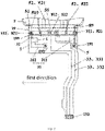
- the display apparatus of the embodiment of the present disclosure includes a display panel 9 and a circuit board assembly Z, where the circuit board assembly Z includes a main circuit board 1 and a jumper connection circuit board 2;
- each "region” refers to a “region” having a certain area partitioned from a plate-shaped structure such as the display panel 9, the main circuit board 1, and the jumper connection circuit board 2, and each region may be provide with some structures therein, but the "region” itself is not a structure.
- electrically coupled between A and B means that structures of A and B may allow an electrical signal to be transmitted therebetween, but does not represent that an electrical signal is necessarily transmitted between A and B; for example, both A and B may be floating, and even there is an electrical connection between A and B, no electrical signal is practically transmitted between A and B.
- a line coupled between A and B means that the line can realize an electrical connection between A and B, but the line may also "pass through” other structures, or other structures may be provided on the line.
- the display panel 9 in the embodiment of the present disclosure is a device having a display function, which includes the display structure 91 provided on the substrate for realizing display.
- the display panel 9 further includes the touch control structure 92 directly formed on a side of the display structure 91 away from the substrate for implementing a touch function, and a signal from the touch control structure 92 is introduced through the first bonding region 99 of the display panel 9.
- the display structure 91 and the touch control structure 92 are both located on the single substrate, rather than being located on two substrates respectively, so that the display panel 9 is of a "FMLOC (Flexible Multi-Layer On Cell) structure".
- FMLOC Flexible Multi-Layer On Cell
- Fig. 1 merely illustrates that the display structure 91 and the touch control structure 92 are distinct functional layers and does not represent the display structure 91 and the touch control structure 92 are two separate layers; in practices, the touch control structure 92 may include a plurality of layer structures sequentially formed on the display structure 91.
- the display panel 9 has the first bonding region 99, and the first display terminals 812 and the first touch control terminals 811, which are respectively provided for providing signals to the display structure 91 and the touch control structure 92, are disposed in the first bonding region 99, where each "terminal" is a bonding pin for bonding.
- the display panel 9 is coupled to the circuit board assembly Z including the main circuit board 1 and the jumper connection circuit board 2.
- Each of the main circuit board 1 and the jumper connection circuit board 2 is a flexible printed circuit (FPC).
- FPC flexible printed circuit
- both the main circuit board 1 and the jumper connection circuit board 2 can be deformed, and thus, on one hand, it is convenient to realize a bonding connection between the main circuit board 1 and the jumper connection circuit board 2; on the other hand, the main circuit board 1 and the jumper connection circuit board 2 may be bent to a back side of the display panel 9 to reduce a bezel of the display apparatus.
- the second bonding region 199 of the main circuit board 1 (MFPC, Main FPC) is bonded to the first bonding region 99 of the display panel 9, the second display terminals 822 and the second touch control terminals 821 are provided in the second bonding region 199, and each of the second display terminals 822 and each of the second touch control terminals 821 are electrically coupled (certainly, physically coupled, i.e., bonded) to a corresponding one of the first display terminals 812 and a corresponding one of the first touch control terminals 811, respectively.
- MFPC Main FPC
- the second display terminals 822 are coupled to ends of the display lines 33 in one-to-one correspondence, and the other end of each of the display lines 33 is coupled to the connection region 193 (in particular, the connector) and coupled to a display signal source (e.g., a main board) through terminals (pins) in the connection region 193 or the like.
- a display signal source e.g., a main board
- the main circuit board 1 is further provided with the touch control chip 4 (touch IC) for providing a touch signal, and at least a portion of the second touch control terminals 821 are coupled to the touch control chip 4 (in particular, pins of the touch control chip 4) through the segment touch control lines 31.
- touch control chip 4 touch IC
- each segment touch control line 31 includes two "segments" separated from each other, i.e., the first segment 311 and the second segment 312, where two ends of the first segment 311 are coupled to one of the main connectors 5 and one of the second touch control terminals 821, respectively, and two ends of the second segment 312 are coupled to another one of the main connectors 5 and the touch control chip 4 (in particular, one pin of the touch control chip 4), respectively.
- the main connectors 5 coupled to the first segments 311 are collectively distributed in the first region 191
- the main connectors 5 coupled to the second segments 312 are collectively distributed in the second region 192.
- the display lines 33 pass through a space between the first region 191 and the second region 192, so that if the main connectors 5 in the first region 191 and the main connectors 5 in the second region 192 are directly coupled by lead lines of the main circuit board 1 (in other words, the segment touch control line 31 is "not segmented"), the lead lines intersect with the display lines 33; in order to avoid misconnection between the lines intersected with each other, the number of layers of the main circuit board 1 needs to be increased, which results in problems of cost increasing, yield reduction and the like.
- the first region 191 and the second region 192 are respectively bonded to the third region 291 and the fourth region 292 of the jumper connection circuit board 2, and specifically, the main connectors 5 in the first region 191 and the second region 192 are respectively electrically coupled (certainly, physically coupled) to the corresponding ones of the jumper connectors 6 in the third region 291 and the fourth region 292.
- the jumper connection circuit board 2 is provided with the plurality of jumper connection lines 313 corresponding to the segment touch control lines 31 one-to-one.
- the first segment 311 and the second segment 312 of each segment touch control line 31 connect two of the main connectors 5, and two of the jumper connectors 6, which are electrically coupled to the two of the main connectors 5 respectively, are coupled by the jumper connection line 313 corresponding to the segment touch control line 31.
- the touch signal is transmitted between the first region 191 and the second region 192 of the main circuit board 1 through the jumper connection line 313 on the jumper connection circuit board 2, and although the jumper connection line 313 crosses the display lines 33 in terms of position, but they belong to different circuit boards, so that they will not misconnect with each other although they cross, and thus the number of layers of the main circuit board 1 and the jumper connection circuit board 2 can be relatively small, which is convenient for reducing the cost (a sum of costs of two circuit boards each with a small number of layers is less than the cost of one multilayer circuit board) and improving the product yield.
- the display structure 91 of the display panel 9 includes a plurality of panel display lines 52, such as data lines 521, a gate driving control line 522 for providing driving signals to a gate driving circuit (GOA), a power supply line 523 for providing power signals (e.g., a positive signal ELVDD, a negative signal ELVSS, etc.), and the like.
- panel display lines 52 such as data lines 521, a gate driving control line 522 for providing driving signals to a gate driving circuit (GOA), a power supply line 523 for providing power signals (e.g., a positive signal ELVDD, a negative signal ELVSS, etc.), and the like.
- Different ones of the panel display lines 52 may correspond to different ones of the display lines 33 on the main circuit board 1, for example, may correspond to a data display line 331, a gate driving display line 332, a positive line 338, a negative line 339, respectively, or the like.
- a portion of the display lines 33 are provided with high frequency signals, such as the signals in the data display lines 331, and the signals in some gate driving display lines 332, and these display lines 33 may be called "MIPI (Mobile Industry Processor interface) lines".
- MIPI Mobile Industry Processor interface
- the panel chip 55 is further disposed on the display panel 9.
- a portion of the panel display lines 52 may enter the panel chip 55 and then be led out to the first display terminals 812, and the number of the lines led out from the display panel 9 may be different from the number of the panel display lines 52, so that the corresponding number of the display lines 33 in the main circuit board 1 may also be different from the number of the panel display lines 52.
- the panel display lines 52 entering the panel chip 55 may include the data lines 521, the gate driving control line 522, and the like; and the power supply line 523 may not pass through the panel chip 55.
- the panel chip 55 may be disposed on the substrate of the display panel 9, or disposed on a chip-on-film (COF) of the display panel 9, which will not be described in detail herein.
- COF chip-on-film
- the display lines 33 on the main circuit board 1 may reach the connection region 193 after passing through some other structures, and for example, reach the connection region 193 after passing through a device in the device region 195 described later.
- the touch signal in the touch control structure 92 may be led out to the first touch control terminal 811 through the panel touch control line 51, and the panel touch control line 51 may not be entirely located in one layer but include portions located in different layers and electrically coupled through a touch through hole 519.
- the display panel 9 further includes a bending region 89 between the display region and the first bonding region 99, such as the bending region 89 between the touch through 519 and the panel chip 55.
- the first bonding region 99 may be bent to the back side of the display region of the display panel to reduce the bezel.
- the jumper connectors 6 coupled to the jumper connection lines 313 are active connectors 61; the jumper connection circuit board 2 further includes a shielding ring 251, the shielding ring 251 surrounding the jumper connection lines 313 and the active connectors 61.
- the "shielding ring 251" being conductive may be formed on the jumper connection circuit board 2, the shielding ring 251 surrounding the jumper connection lines 313 and the corresponding ones of the jumper connectors 6 (i.e., the active connectors 61) inside, so that an influence of an external signal on a signal in the jumper connection line 313 may be shielded.
- jumper connectors 6 coupled with the shielding ring 251 to introduce a particular signal to the shielding ring 251 to improve a shielding effect.
- the shielding connector 62 may be coupled to the shielding ring 251 by a lead line.
- the shielding connector 62 may be "directly located on the shielding ring 251", for example, two shielding connectors 62 in the third region 291 may be directly coupled, two shielding connectors 62 in the fourth region 292 may be directly coupled, then one of the shielding connectors 62 in the third region 291 is coupled with one of the shielding connectors 62 in the fourth region 292, and the other of the shielding connectors 62 in the third region 291 is coupled with the other of the shielding connectors 62 in the fourth region 292, which finally form the shielding ring 251.
- the shielding connectors 62 "directly on the shielding ring 251" above may be a connectors located at "outermost edges" of the respective regions, such as the two jumper connectors 6 uppermost and lowermost on the leftmost side and the two jumper connectors 6 uppermost and lowermost on the rightmost side in Fig. 6 .
- each of the third region 291 and the fourth region 292 there is the jumper connector 6 (i.e., the ground connector 63) coupled to the ground (i.e., the ground terminal 631) to further stabilize signals of the jumper connectors 6.
- the jumper connector 6 i.e., the ground connector 63
- the ground i.e., the ground terminal 631
- the jumper connectors 6 i.e., the floating connectors 64 which are not coupled (floating) at all, and these floating connectors 64 are only provided for bonding with the corresponding ones of the main connectors 5 (certainly, these main connectors 5 should also be floating) in the first region 191 and the second region 192, so as to improve a bonding effect and stabilize connections.
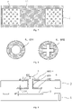
- the jumper connection circuit board 2 includes a first base layer, and a first conductive layer and a second conductive layer are respectively disposed on two sides of the first base layer; each jumper connector 6 includes a first contact part 691 provided in the first conductive layer and a second contact part 692 provided in the second conductive layer, the first contact part 691 and the second contact part 692 being coupled by a connection part 693 in a through hole of the first base layer.
- the jumper connection circuit board 2 may be a double-layer circuit board, which includes the first base layer made of plastic or the like and being insulated, and the first conductive layer and the second conductive layer made of a conductive material such as copper are respectively disposed on two sides of the first base layer.
- conductive layer refers to conductive structures located on a particular side of the base layer and does not represent that each conductive layer is a complete layer.
- the number of layers of the "double-layer circuit board” is described with reference to the number of conductive layers therein, and does not represent the total number of layers of the circuit board, i.e., the circuit board may have other layer structures therein.
- the double-layer circuit board typically includes a base layer X1 of PI (polyimide) material, which may have a thickness ranging from 23 ⁇ m to 28 ⁇ m, for example, may be 25.4 ⁇ m; two conductive layers X2 of copper metal are respectively provided on two sides of the base layer XI, the conductive layers X2 each may have a thickness ranging from 12 ⁇ m to 16 ⁇ m, for example, may be 14 ⁇ m; two glue layers X3 are respectively provided on sides of the two conductive layers X2 away from the base layer XI, and the glue layers X3 each may have a thickness ranging from 13 ⁇ m to 17 ⁇ m, for example, may be 15 ⁇ m; two PI protective layers (Coverlay) X4 are respectively provided on sides of the two glue layers X3 away from the base layer XI, and the PI protective layers X4 each may have a thickness ranging from 11 ⁇ m to 14 ⁇ m, for example, may be 12.7 ⁇ m;
- PI polyimide
- the jumper connector 6 may simultaneously connect two conductive layers of the jumper connection circuit board 2, specifically, contact parts (the first contact part 691 and the second contact part 692) are respectively provided in the two conductive layers, and a through hole is formed in the first base layer between the two conductive layers, and the connection part 693 of a conductive material is formed in the through hole, so that the connection part 693 and the two contact parts (the first contact part 691 and the second contact part 692) jointly constitute the jumper connector 6.
- a surface of first contact part 691 distal from the first base layer is of a pattern with an opening therein, and a surface of the second contact part 692 distal from the first base layer is of a pattern with an opening therein;
- the connection part 693 is a hollow cylinder;
- the jumper terminal 6 is electrically coupled to the main connector 5 by a soldering structure 7 formed by melting solder in a hollow of the connection part.
- connection part 693 is hollow cylindrical (i.e., the connection part 693 does not fully "fill” the through hole), and thus the first contact part 691 and the second contact part 692 are both hollowed.
- the solder e.g., tin solder
- the solder may be provided in the hollow in advance, and then the solder may be melted by heating through a process such as returning to a furnace, so that the melted solder forms the soldering structure 7 to electrically connect (certainly, physically connect, or bond) the jumper connector 6 with the main connector 5.
- a surface of the first contact part 691 away from the first base layer is a circular ring
- a surface of the second contact part 692 away from the first base layer is a circular ring
- the connection part 693 is hollow cylindrical.
- the first contact part 691 and the second contact part 692 each may be a circular ring, that is, an outer edge thereof is circular and an inner opening thereof is circular.
- an inner diameter of the circular ring ranges from 0.05mm to 0.15mm, and an outer diameter of the circular ring ranges from 0.25mm to 0.35mm; a surface of the main connector 5 proximal to the first base layer is a circle, and a diameter of the circle ranges from 0.25mm to 0.35mm.
- the inner diameter of the circular ring of each of the contact parts may range from 0.05mm to 0.15mm, and the outer diameter of the circular ring of each of the contact parts may range from 0.25mm to 0.35mm; correspondingly, the main connector 5 on the main circuit board 1 has a shape of a circle, and a diameter of the circle ranges from 0.25mm to 0.35mm.
- an outer edge of a surface of the first contact part 691 away from the first base layer is circular; an outer edge of a surface of the second contact part 692 away from the first base layer is circular.
- each of the contact parts may be circular.
- the opening in the pattern of the surface of the first contact part 691 away from the first base layer has a shape formed by two strips intersecting with each other; the opening in the pattern of the surface of the second contact part 692 away from the first base layer has a shape formed by two stripes intersecting with each other.
- each of the contact parts has a shape formed by two strips intersecting with each other, for example, a shape of " ⁇ " or a shape of "+".
- the outer dimension of the surface of the first contact part 691 away from the first base layer is different from the outer dimension of the surface of the second contact part 692 away from the first base layer.
- outer edges of two contact parts of each of the jumper connectors 6 may have different dimensions, for example, outer diameters of circular rings may be different, the outer diameter of one circular ring is larger and the outer diameter of the other circular ring is smaller, so that the soldering structure 7 can be formed into a desired shape to achieve better connection.
- the soldering structure 7 may include a "soldering cap” on a side of the jumper connector 6 away from the main connector 5, and a “soldering part" between the jumper connector 6 and the main connector 5, and specific forms of the soldering cap and the soldering part may be various.
- soldering structures 7 each have a soldering cap (a thickness D2 of which is generally less than 0.05mm), while a portion of soldering structures 7 have almost no soldering cap; and for example, soldering caps of a portion of soldering structures 7 each are symmetrical left and right (based on a direction in the figure), and are substantially positioned in a middle of the ring; while soldering caps of a portion of soldering structures 7 may be significantly offset to left or right.
- the "soldering part" of each of a portion of soldering structures 7 may be located substantially in the middle of the ring; while the "soldering part" of each of a portion of soldering structures 7 may be significantly offset to left or right.
- a width of the soldering part may be first reduced and then increased, that is, the soldering part is in a form of "thin middle and thick ends"; alternatively, further referring to Fig. 16 , the width of the soldering part is continuously reduced in the direction in which the jumper connector 6 is directed toward the main connector 5.
- thermosetting adhesive may be provided to directly bond and fix the circuit boards at positions without connectors, and a thickness of a layer of the adhesive may be about 5 ⁇ m.
- a certain gap may be provided between the main circuit board 1 and the jumper connection circuit board 2, and other materials for isolation may also be filled in the gap.
- the circuit boards each may be provided with other conductive structures (e.g., various lead lines) in addition to the jumper connectors 6 and the main connectors 5.
- other conductive structures e.g., various lead lines
- a portion of the jumper connection lines 313 are disposed in the first conductive layer, and the rest of the jumper connection lines 313 are disposed in the second conductive layer; the first conductive layer is provided with at least one shielding mesh 252, and the second conductive layer is provided with at least one shielding mesh 252.
- different ones of the jumper connection lines 313 may be respectively distributed in the first conductive layer and the second conductive layer, and such distribution is beneficial to reducing wiring density in each conductive layer, increasing a pitch between the lines, avoiding accidental short circuit, and reducing interference.
- the shielding mesh 252 formed into a grid-shape and made of a conductive metal may be provided at a position of each conductive layer where there is no jumper connection line 313 and no jumper connector 6, so as to shield the influence of an external signal on the jumper connection lines 313.
- the shielding ring 251 may be provided in each conductive layer.
- all the jumper connection lines 313 are provided in the first conductive layer; the second conductive layer is provided with a shielding layer 253 at least at positions corresponding to the jumper connection lines 313; the second conductive layer is closer to the main circuit board 1 than the first conductive layer.
- the jumper connection lines 313 may be provided in one conductive layer (the first conductive layer); accordingly, referring to Fig. 7 , the other conductive layer (the second conductive layer) may have the shielding layer 253 being integral (certainly, no shielding layer at positions corresponding to the jumper connectors 6), and the second conductive layer is closer to the main circuit board 1 than the first conductive layer, or the shielding layer 253 is located between the jumper connection lines 313 and the display lines 33.
- a part of the jumper connection circuit board 2 provided with the third region 291 and a part of the jumper connection circuit board 2 provided with the fourth region 292 are asymmetric.
- structures of both ends (an end provided with the third region 291 and an end provided with the fourth region 292) of the jumper connection line board 2 may be "asymmetric" (i.e., have a "fool-proof” design), so that an operator can distinguish the third region 291 from the fourth region 292 to avoid misconnections.
- an asymmetric structure of the part of the jumper connection circuit board 2 provided with the third region 291 and the part of the jumper connection circuit board 2 provided with the fourth region 292 is realized by at least one of following modes:
- the "asymmetric" structure at both ends of the jumper connection circuit board 2 may be achieved in many different specific modes.
- specific conductive patterns i.e., patterns formed by structures of the conductive layers
- the jumper connection circuit board 2 corresponding to the third region 291 and the fourth region 292 may be different in each conductive layer.
- the jumper connection circuit board 2 (the first base layer) itself may have an "asymmetric" shape at both ends thereof.
- the specific conductive patterns in each conductive layer may be symmetrically distributed, but asymmetric "optical marks 26" are provided at the ends where the third region 291 and the fourth region 292 are located, for example, two optical marks 26 are provided at one end, and only one optical mark 26 is provided at the other end.
- the main circuit board 1 further includes a plurality of direct-connection touch control lines 32, and each direct-connection touch control line 32 is coupled between the touch control chip 4 and one of the second touch control terminals 821.
- the direct-connection touch control lines 32 that is, touch control lines directly connecting the touch control chip 4 with the second touch control terminals 821, and these direct-connection touch control lines 32 do not intersect with the display lines 33, and thus they can be directly disposed.
- the display panel 9 includes a plurality of panel touch control lines 51 for introducing touch signals into the first touch control terminals 811 respectively; the number of the panel touch control lines 51 is equal to a sum of the number of the segment touch control lines 31 and the number of the direct-connection touch control lines 32.
- the touch signals in the touch control structure need to be respectively introduced to the first touch control terminals 811 through the panel touch control lines 51, and thus the panel touch control lines 51 correspond to the first touch control terminals 811 one by one, and also correspond to touch electrodes (e.g., sensing electrodes and scanning electrodes) in the display panel one by one.
- touch electrodes e.g., sensing electrodes and scanning electrodes
- a total number of the touch control lines (the segment touch control lines 31 and the direct-connection touch control lines 32) should be the same as the number of the panel touch control lines 51.
- the touch control structure 92 includes a plurality of sensing electrodes and a plurality of scanning electrodes overlapped and insulated; each of the sensing electrodes is electrically coupled with one of the first touch control terminals 811 (specifically, through one of the panel touch control lines 51), the first touch control terminals 811 electrically coupled with the sensing electrodes are first sensing touch control terminals 8112, and the second touch control terminals 821 electrically coupled with the first sensing touch control terminals 8112 are second sensing touch control terminals 8212; each of the scanning electrodes is electrically coupled to one of the first touch control terminals 811 (specifically, by one of the panel touch control lines 51), the first touch control terminals 811 electrically coupled to the scanning electrodes are first scanning touch control terminals 8111, and the second touch control terminals 821 electrically coupled to the first scanning touch control terminals 8111 are second scanning touch control terminals 8211; each of the direct-connection touch control lines 32 is coupled with one of the second sensing touch control terminals 8212;
- the touch control structure 92 in the display panel 9 may be formed by sensing electrodes (Rx) and scanning electrodes (Tx) which are overlapped.
- the scanning electrodes are applied with scanning signals in turn, so that a position of touch can be determined by detecting signals in the sensing electrodes.
- the touch control terminals (the second sensing touch control terminals 8212) electrically coupled to the sensing electrodes in the main circuit board 1 are coupled to the touch control chip 4 through the direct-connection touch control lines 32, and the touch control terminals (the second scanning touch control terminals 8211) electrically coupled to the scanning electrodes are coupled to the touch control chip 4 through the segment touch control lines 31.
- the first direction is the direction in which the width of the second bonding region 199 extends, that is, a direction in which different terminals (the touch control terminals and the display terminals) are sequentially arranged (for example, a direction from right to left in Figs.
- the second bonding region 199 is first provided with the second scanning touch control terminals 8211, then the second display terminals 822, and then the second sensing touch control terminals 8212, that is, the second scanning touch control terminals 8211 are located at a "right end" of the main circuit board 1, the second display terminals 822 are located at a "middle part" of the main circuit board 1, and the second sensing touch control terminals 8212 are located at a "left end" of the main circuit board 1; accordingly, the second region 192 and the first region 191 are also located at left and right sides of the display lines 33, respectively.
- the circuit board may have a shape similar to a word "7", the second bonding region 199, the first region 191, the second region 192, etc. are located at a “horizontal part” of the word “7 “, the connection region 193 is located at a lower end of a “vertical part” of the word “7 “, and the display lines 33 extend downward from a middle of the second bonding region 199 to the connection region 193;
- the direct-connection touch control lines 32 (the touch control lines corresponding to the sensing electrodes) extend downward slightly from a left end of the second bonding region 199, i.e., are directly coupled to the touch control chip 4;
- the first segment 311 of the segment touch control line 31 (the touch control line corresponding to the scanning electrode) extends from a right end of the second bonding region 199 slightly downward into the first region 191 and is coupled to the main connector 5, and then crosses each display line 33 to be coupled to the second region 192 at left through the jumper connection line
- the maximum width (i.e., the dimension in a direction parallel to the horizontal part of the word "7") of the main circuit board 1 may range from 50mm to 60mm, for example, may be 55.4mm ⁇ 0.15mm; a width of the second bonding region 199 may be slightly smaller, and may range from 50mm to 60mm, for example, may be 53.7mm ⁇ 0.15mm, and a height of the second bonding region 199 (i.e., the dimension in a direction perpendicular to the horizontal part of the word "7") may range from 1mm to 2mm, for example, maybe 1.4mm ⁇ 0.2mm.
- the touch control structure 92 includes a plurality of sensing electrodes and a plurality of scanning electrodes overlapped and insulated; each of the sensing electrodes is electrically coupled with one of the first touch control terminals 811 (specifically, through one of the panel touch control lines 51), the first touch control terminals 811 electrically coupled with the sensing electrodes are first sensing touch control terminals 8112, and the second touch control terminals 821 electrically coupled with the first sensing touch control terminals 8112 are second sensing touch control terminals 8212; each scanning electrodes is electrically coupled to one of the first touch control terminals 811 (specifically, by one of the panel touch control lines 51), the first touch control terminals 811 electrically coupled to the scanning electrodes are first scanning touch control terminals 8111, and the second touch control terminals 821 electrically coupled to the first scanning touch control terminals 8111 are second scanning touch control terminal 8211; each direct-connection touch control lines 32 is coupled with one of the second scanning touch control terminals 8211; the first segment 311 of
- the second scanning touch control terminal 8211 may be directly coupled to the touch control chip 4 through the direct-connection touch control line 32, and the second sensing touch control terminal 8212 is coupled to the touch control chip 4 through the segment touch control line 31.
- the second scanning touch control terminal 8211 is closer to the touch control chip 4, and the second sensing touch control terminal 8212 is farther away from the touch control chip 4.
- the main circuit board 1 may include a second base layer, and a third conductive layer and a fourth conductive layer may be provided on two sides of the second base layer respectively.
- the main circuit board 1 may be in a form of a double-layer circuit board.
- the display lines 33 are disposed in the fourth conductive layer; the third conductive layer is provided with a shielding structure at least at positions corresponding to the display lines 33; the third conductive layer is closer to the jumper connection circuit board 2 than the fourth conductive layer.
- the display lines 33 may be located in the conductive layer (the fourth conductive layer) farther from the patch circuit board 2, and correspondingly, in another conductive layer (the third conductive layer) closer to the jumper connection circuit board 2, a shielding structure (such as a layered structure or a mesh structure) may be provided at positions corresponding to the display lines 33, and the shielding structure may further shield the influence of the display lines 33 (especially, the display lines 33 transmitting high frequency signals) on the jumper connection lines 313 in the jumper connection circuit board 2.
- a shielding structure such as a layered structure or a mesh structure
- the segment touch control lines 31 are all provided in one of the third conductive layer and the fourth conductive layer.
- all the segment touch control lines 31 may be located in a same conductive layer.
- a portion of the segment touch control lines 31 are provided in the third conductive layer, and the rest of the segment touch control line 31 are provided in the fourth conductive layer.
- different segment touch control lines 31 may be respectively located in different conductive layers to reduce wiring density in each conductive layer.
- the main circuit board 1 has a device region 195; in the device region 195, a plurality of devices are provided on a side of the main circuit board 1; the touch control chip 4 is arranged on the side of the device region 195 of the main circuit board 1, which is provided with a device; in the device region 195, a metal supporting layer 1951 is provided on a side of the main circuit board 1, which is opposite to the side on which the device is provided.
- the main circuit board 1 further has the device region 195 for disposing a large number of additional devices (such as capacitors, etc.), and simultaneously, the touch control chip 4 is also located in the device region 195 (because the touch control chip 4 is also a device).
- additional devices such as capacitors, etc.
- a mode of the embodiment of the present disclosure there may be two device regions 195, which may be located below the second bonding region 199, and the first region 191 and the second region 192, etc. are located below the device regions 195.
- the devices, the touch control chip 4, and the lines (the direct-connection touch control lines 32, the segment touch control lines 31, the display lines 33, etc.) in the device region 195 may be located on a same side of the main circuit board 1 (i.e., in the same conductive layer), and the other side of the device region 195 is provided with an integral metal layer (the metal supporting layer 1951) with a larger thickness, so that with the metal supporting layer 1951, a portion of the main circuit board 1 in the device region 195 has higher strength, and various devices disposed therein are protected.
- a boundary of an orthographic projection of the metal supporting layer 1951 on the main circuit board 1 exceeds a boundary of the device region 195 by at least 0.5mm.
- the metal supporting layer 1951 may be "larger" than the device region 195 by at least 0.5mm (or more) at each side edge; for example, referring to Fig. 10 , two device regions 195 may correspond to one larger metal supporting layer 1951.
- the main connectors 5 are arranged in an array, in any two adjacent rows of the array, any two main connectors 5 respectively belonging to different rows are at different positions in a row direction, and in any two adjacent columns of the array, any two main connectors 5 respectively belonging to different columns are at different positions in a column direction; in any one of the third region 291 and the fourth region 292, the jumper connectors 6 are arranged in an array, in any two adjacent rows of the array, any two jumper connectors 6 respectively belonging to different rows are at different positions in a row direction, and in any two adjacent columns of the array, any two jumper connectors 6 respectively belonging to different columns are at different positions in a column direction.
- the connectors (the main connectors 5 or the jumper connectors 6) in each region may be arrayed in rows and columns; furthermore, adjacent rows/columns are "staggered", and thus for each connector, it is not aligned with any other connector, in the row/column adjacent thereto, in the row/column direction, which facilitates connections between the connectors inside the array and the corresponding lines (the first segment 311 or the second segment 312 of the segment touch control line 31, and the jumper connection lines 313), i.e., the lines can easily bypass outer connectors to connect inner connectors.
- the array of the main connectors 5 includes seven rows and seven columns, where there are four main connectors 5 in each odd-numbered row, three main connectors 5 in each even-numbered row, four main connectors 5 in each odd-numbered column, and three main connectors 5 in each even-numbered column; in any one of the third region 291 and the fourth region 292, the array of the jumper connectors 6 includes seven rows and seven columns, where there are four jumper connectors 6 in each odd-numbered row, three jumper connectors 6 in each even-numbered row, four jumper connectors 6 in each odd-numbered column, and three jumper connectors 6 in each even-numbered column.
- the connectors (the main connectors 5 or the jumper connectors 6) in each region may be arranged in an array having seven rows and seven columns, where there are four connectors in each odd-numbered row/column and three connectors in each even-numbered row/column, i.e., each connector in each even-numbered row/column is located between the connectors in the odd-numbered row/column.
- Each region may have a size of 3.84mm*3.84mm; in a same region, the distance (based on the distance between centers of circles) between the two connectors farthest from each other in the row/column direction may range from 2.54mm to 2.79mm, which may have an error of ⁇ 0.05mm.
- the display panel 9 is an organic light emitting diode display panel; the display structure 91 of the organic light emitting diode display panel includes a plurality of organic light emitting diodes.
- the display panel 9 may be an organic light emitting diode (OLED) display panel 9; accordingly, the display structure 91 thereof includes a plurality of organic light emitting diodes for emitting light.
- OLED organic light emitting diode
- each organic light emitting diode has a positive electrode and a negative electrode (or a cathode and an anode), respectively.
- the first display terminals 812 there are a plurality of first positive display terminals for supplying power to positive electrodes of the organic light emitting diodes and a plurality of first negative display terminals for supplying power to negative electrodes of the organic light emitting diodes;
- the second display terminals 822 electrically coupled with the first positive display terminals are second positive display terminals, and the second display terminals 822 electrically coupled with the first negative display terminals are second negative display terminals;
- the display line 33 includes a plurality of positive lines 338 coupled to the second positive display terminals and a plurality of negative lines 339 coupled to the second negative display terminals.
- the second display terminals 822 of the main circuit board 1 include the second positive display terminals for supplying power to the positive electrodes of the organic light emitting diodes and the second negative display terminals for supplying power to the negative electrodes of the organic light emitting diodes.
- the display lines 33 of the main circuit board 1 include a plurality of positive lines 338 (ELVDD) for supplying power to the positive electrodes of the organic light emitting diodes, and a plurality of negative lines 339 (ELVSS) for supplying power to the negative electrodes of the organic light emitting diodes.
- each of the positive lines 338 and the negative lines 339 may be coupled to a plurality of corresponding ones of the display terminals (the second positive display terminals, the second negative display terminals), i.e., electrode lines (the positive lines 338 and the negative lines 339) may be relatively "thick" to avoid short-circuiting and the like.
- the lead lines in the display panel 9 corresponding to the positive lines 338 and the negative lines 339 may not pass through the panel chip 55.
- the second display terminal 822 corresponding to a high frequency signal (e.g., corresponding to a signal of the data line 521) may be located at middle, and the second display terminals 822 (e.g., the second positive display terminals, the second negative display terminals) for providing other relatively low frequency signals or a constant signal may be located at two ends.
- the display structure 91 of the organic light emitting diode display panel further includes an encapsulation layer covering each organic light emitting diode;
- the OLEDs may be encapsulated by the encapsulation layer, and the corresponding touch control structure 92 may then be fabricated on the encapsulation layer, and the touch control structure 92 is electrically coupled to the first touch control terminals 811 in the first bonding region 99 through a structure such as a touch through hole 519.
- the polarizer 93 for reducing reflected light is disposed on the side of the touch control structure 92 away from the substrate, and the cover plate 94 (e.g., a glass plate) for protecting other structures is disposed on the side of the polarizer 93 away from the substrate.
- the cover plate 94 e.g., a glass plate
- the above structure is only an example of the structure of the display panel 9, and is not a specific limitation on a form of the display panel 9.
- a thickness of each of the first touch control terminals 811 is less than a thickness of the display structure 91; a thickness of each of the first display terminals 812 is less than the thickness of the display structure 91.
- the thickness of a structure refers to its largest dimension in the direction perpendicular to the substrate.
- each "terminal” may be formed by stacking one or more of the metal layers, but a total thickness of the "terminal” should not exceed the thickness of the display structure 91 or not reach the touch control structure 92.
- the display panel 9 includes data lines 521 and panel touch control lines 51 for introducing touch signals into the first touch control terminals 811 respectively, and there is a first distance between the panel touch control lines 51 and the data lines 521 in a direction perpendicular to the substrate;
- the first distance is less than the second distance.
- the panel touch control lines 51 and the data lines 521 may be located in different layers so that there is a certain distance (the first distance) therebetween in the direction perpendicular to the substrate; in the circuit board assembly Z, the display lines 33 and the jumper connection lines 313 (corresponding to a portion of the touch control lines) overlap each other, so that there is a certain distance (the second distance) between the display lines and the jumper connection lines in the direction perpendicular to the substrate, in such case, the first distance is different from the second distance, for example, the first distance is less than the second distance.
- the display panel 9 includes the data lines 521;
- the display panel 9 has the data lines 521, so that the display lines 33 of the main circuit board 1 include the data display lines 331 for providing signals to the data lines 521, and since the panel chip 55 is provided, the number of the data display lines 331 is less than the number of the data lines 521, i.e., more data lines 521 can be provided with signals by fewer data display lines 331 (for example, one data display line 331 provides signals to a plurality of data lines 521 in turn).
- a width of each of the data lines 521 is less than a width of each of the data display lines 331.
- the width of each of the data display lines 331 can be relatively large.
- the present disclosure provides a display apparatus including a display panel 9 and a circuit board assembly Z including a main circuit board 1 and a jumper connection circuit board 2;
- the thickness D2 of a part (i.e., "soldering cap") of the soldering structure 7 farther from the main circuit board 1 than the first contact part 691 is less than or equal to 0.05mm.
- the display panel 9 includes the data lines 521;
- the display panel 9 includes the data lines 521 and the panel touch control lines 51 for introducing touch signals into the first touch control terminals 811 respectively, and there is a first distance between the panel touch control lines 51 and the data lines 521 in a direction perpendicular to the substrate;
- the jumper connectors 6 coupled to the jumper connection lines 313 are active connectors 61; the jumper connection line panel 2 further includes a shielding ring 251, the shielding ring 251 surrounding the jumper connection lines 313 and the active connectors 61.
- the display panel 9 is an organic light emitting diode display panel; the display structure 91 of the organic light emitting diode display panel includes a plurality of organic light emitting diodes;
Landscapes
- Engineering & Computer Science (AREA)
- Physics & Mathematics (AREA)
- Theoretical Computer Science (AREA)
- General Engineering & Computer Science (AREA)
- General Physics & Mathematics (AREA)
- Human Computer Interaction (AREA)
- Nonlinear Science (AREA)
- Microelectronics & Electronic Packaging (AREA)
- Mathematical Physics (AREA)
- Chemical & Material Sciences (AREA)
- Crystallography & Structural Chemistry (AREA)
- Optics & Photonics (AREA)
- Devices For Indicating Variable Information By Combining Individual Elements (AREA)
- Manufacturing & Machinery (AREA)
- Electroluminescent Light Sources (AREA)
- Health & Medical Sciences (AREA)
- Electromagnetism (AREA)
- Toxicology (AREA)
Abstract
Description
- The present application claims the priority of
Chinese Patent Application No. 202020318481.1, filed on March 13, 2020 Chinese Patent Application No. 202010505842.8, filed on June 5, 2020 - The present disclosure relates to the field of display technology, and particularly relates to a display apparatus.
- A display panel may be bonded to a circuit board, and the circuit board is then coupled to a display signal source such as a motherboard, so that a display driving signal is introduced into the display panel through a lead line in the circuit board. For the display panel with a touch function, a touch signal may also be transmitted through the circuit board, so that the number of lead lines in the circuit board is further increased.
- In order to avoid misconnection between the lead lines in the circuit board or an excessive density of the lead lines in the circuit board, the number of layers for wiring may need to be increased, thereby causing problems of cost increasing, yield reduction and the like.
- In a first aspect, the present disclosure provides a display apparatus, including a display panel, a circuit board assembly, where the circuit board assembly includes a main circuit board and a jumper connection circuit board;
- the display panel includes a substrate, a display structure arranged on the substrate and a touch control structure arranged on a side of the display structure away from the substrate; the display panel has a first bonding region, and a plurality of first display terminals electrically coupled with the display structure and a plurality of first touch control terminals electrically coupled with the touch control structure are arranged in the first bonding region;
- the display panel includes a panel chip;
- the main circuit board is provided with a second bonding region, a connection region, a first region and a second region; the second bonding region is bonded with the first bonding region, and a plurality of second display terminals electrically coupled with the first display terminals respectively and a plurality of second touch control terminals electrically coupled with the first touch control terminals respectively are arranged in the second bonding region; a plurality of main connectors are respectively arranged in the first region and the second region;
- the main circuit board includes a touch control chip, a plurality of display lines and a plurality of segment touch control lines; each segment touch control line includes a first segment and a second segment, where the first segment is coupled between one of the second touch control terminal and one of the main connectors in the first region, and the second segment is coupled between the touch control chip and one of the main connectors in the second region; at least a portion of the display lines are coupled between the second display terminals and the connection region, and intersect with a line connected between the first region and the second region;
- the jumper connection circuit board has a third region and a fourth region; the third region is bonded with the first region, and the fourth region is bonded with the second region; a plurality of jumper connectors electrically coupled with the main connectors in the first region respectively are arranged in the third region, and a plurality of jumper connectors electrically coupled with the main connectors in the second region respectively are arranged in the fourth region;
- the jumper connection circuit board includes a plurality of jumper connection lines which correspond to the segment touch control lines one by one; each jumper connection line is coupled between one of the jumper connectors in the third region and one of the jumper connectors in the fourth region, and two of the main connectors electrically coupled with such two jumper connectors are respectively coupled with the first segment and the second segment of one of the segment touch control lines;
- the main circuit board is a flexible circuit board; the jumper connection circuit board is a flexible circuit board.
- In some implementations, the jumper connectors coupled to the jumper connection lines are active connectors;
the jumper connection circuit board further includes a shielding ring, and the shielding ring surrounds the jumper connection lines and the active connectors. - In some implementations, at least one of the jumper connectors in the third region is a shielding connector coupled to the shielding ring;
at least one of the jumper connectors in the fourth region is a shielding connector coupled to the shielding ring. - In some implementations, at least one of the jumper connectors in the third region is a ground connector coupled to a ground terminal;
at least one of the jumper connectors in the fourth region is a ground connector coupled to the ground terminal. - In some implementations, at least one of the jumper connectors in the third region is a floating connector floating;
at least one of the jumper connectors in the fourth region is a floating connector floating. - In some implementations, the jumper connection circuit board includes a first base layer, where a first conductive layer and a second conductive layer are respectively arranged on two sides of the first base layer;
each jumper connector includes a first contact part arranged in the first conductive layer and a second contact part arranged in the second conductive layer, and the first contact part and the second contact part are coupled through a connection part in a through hole of the first base layer. - In some implementations, a surface of the first contact part away from the first base layer is of a pattern with an opening therein, and a surface of the second contact part away from the first base layer is of a pattern with an opening therein;
the connection part is a hollow cylinder; the jumper connector is electrically coupled with the main connector through a soldering structure formed by melting solder in a hollow of the connection part. - In some implementations, the surface of the first contact part away from the first base layer has a shape of a circular ring, the surface of the second contact part away from the first base layer has a shape of the circular ring, and the connection part is hollow cylindrical;
- an inner diameter of the circular ring ranges from 0.05mm to 0.15mm, and an outer diameter of the circular ring ranges from 0.25mm to 0.35mm;
- a surface of the main connector proximal to the first base layer has a shape of a circle, and a diameter of the circle ranges from 0.25mm to 0.35mm.
- In some implementations, an outer edge of the surface of the first contact part away from the first base layer has a shape of a circle;
an outer edge of the surface of the second contact part away from the first base layer has a shape of a circle. - In some implementations, the opening in the pattern of the surface of the first contact part away from the first base layer is in a shape formed by two strips intersecting with each other;
the opening in the pattern of the surface of the second contact part away from the first base layer is in a shape formed by two strips intersecting with each other. - In some implementations, an outer edge of the surface of the first contact part away from the first base layer has a dimension different from that of an outer edge of the surface of the second contact part away from the first base layer.
- In some implementations, a portion of the jumper connection lines are arranged in the first conductive layer, and the rest of the jumper connection lines are arranged in the second conductive layer;
the first conductive layer is provided with at least one shielding mesh, and the second conductive layer is provided with at least one shielding mesh. - In some implementations, the jumper connection lines are all disposed in the first conductive layer;
- the second conductive layer is provided with a shielding layer at least at a position corresponding to the jumper connection lines;
- the second conductive layer is closer to the main circuit board than the first conductive layer.
- In some implementations, a part of the jumper connection circuit board provided with the third region and a part of the jumper connection circuit board provided with the fourth region are in an asymmetric structure.
- In some implementations, the part of the jumper connection circuit board provided with the third region and the part of the jumper connection circuit board provided with the fourth region being in the asymmetric structure is implemented by at least one of following modes:
- a conductive pattern in the part of the jumper connection circuit board provided with the third region and a conductive pattern in the part of the jumper connection circuit board provided with the fourth region are in an asymmetric structure;
- a shape of the part of the jumper connection circuit board provided with the third region and a shape of the part of the jumper connection circuit board provided with the fourth region are in an asymmetric structure;
- the part of the jumper connection circuit board provided with the third region and the part of the jumper connection circuit board provided with the fourth region are provided with asymmetrical optical marks.
- In some implementations, the main circuit board further includes a plurality of direct-connection touch control lines, and each direct-connection touch control line is coupled between the touch control chip and one of the second touch control terminals.
- In some implementations, the display panel includes a plurality of panel touch control lines for introducing touch signals to the first touch control terminals;
the number of the panel touch control lines is equal to a sum of the number of the segment touch control lines and the number of the direct-connection touch control lines. - In some implementations, the touch control structure includes a plurality of sensing electrodes and a plurality of scanning electrodes overlapped and insulated;
- each sensing electrode is electrically coupled with one of the first touch control terminals, the first touch control terminals electrically coupled with the sensing electrodes are first sensing touch control terminals, and the second touch control terminals electrically coupled with the first sensing touch control terminals are second sensing touch control terminals;
- each scanning electrode is electrically coupled with one of the first touch control terminals, the first touch control terminals electrically coupled with the scanning electrodes are first scanning touch control terminals, and the second touch control terminals electrically coupled with the first scanning touch control terminals are second scanning touch control terminals;
- each direct-connection touch control line is coupled with one of the second sensing touch control terminals; the first segment of each of the segment touch control lines is coupled with one of the second scanning touch control terminals;
- in the second bonding region, along a first direction, the second scanning touch control terminals, the second display terminals and the second sensing touch control terminals are arranged in sequence; the first direction is parallel to a direction in which a width of the second bonding region extends.
- In some implementations, the touch control structure includes a plurality of sensing electrodes and a plurality of scanning electrodes overlapped and insulated;
- each sensing electrode is electrically coupled with one of the first touch control terminals, the first touch control terminals electrically coupled with the sensing electrodes are first sensing touch control terminals, and the second touch control terminals electrically coupled with the first sensing touch control terminals are second sensing touch control terminals;
- each scanning electrode is electrically coupled with one of the first touch control terminals, the first touch control terminals electrically coupled with the scanning electrodes are first scanning touch control terminals, and the second touch control terminals electrically coupled with the first scanning touch control terminals are second scanning touch control terminals;
- each direct-connection touch control line is coupled with one of the second scanning touch control terminals; the first segment of each of the segment touch control lines is coupled with one of the second sensing touch control terminals;
- in the second bonding region, along a first direction, the second sensing touch control terminals, the second display terminals and the second scanning touch control terminals are arranged in sequence; the first direction is parallel to a direction in which a width of the second bonding region extends.
- In some implementations, the main circuit board includes a second base layer, and a third conductive layer and a fourth conductive layer are respectively disposed on two sides of the second base layer.
- In some implementations, the display lines are all arranged in the fourth conductive layer; the third conductive layer is provided with a shielding structure at least at positions corresponding to the display lines;
the third conductive layer is closer to the jumper connection circuit board than the fourth conductive layer. - In some implementations, the segment touch control lines are all provided in one of the third conductive layer and the fourth conductive layer;
alternatively, a portion of the segment touch control lines are arranged in the third conductive layer, and the rest of the segment touch control lines are arranged in the fourth conductive layer. - In some implementations, the main circuit board has a device region;
- in the device region, a plurality of devices are arranged on a side of the main circuit board;
- the touch control chip is arranged on a side of the device region of the main circuit board provided with the devices;
- in the device region, a metal supporting layer is arranged on a side of the main circuit board opposite to the side provided with the devices.
- In some implementations, a boundary of an orthographic projection of the metal supporting layer on the main circuit board exceeds a boundary of the device region by at least 0.5mm.
- In some implementations, in any one of the first region and the second region, the main connectors are arranged in an array, any two of the main connectors, which are respectively in different rows, in any two adjacent rows of the array are at different positions in a row direction, and any two of the main connectors, which are respectively in different columns, in any two adjacent columns of the array are at different positions in a column direction;
in any one of the third region and the fourth region, the jumper connectors are arranged in an array, any two jumper connectors, which are respectively in different rows, in any two adjacent rows of the array are at different positions in the row direction, and any two jumper connectors, which are respectively in different columns, in any two adjacent columns of the array are at different positions in the column direction. - In some implementations, in any one of the first region and the second region, the array of the main connectors includes seven rows and seven columns, with four of the main connectors in each odd-numbered row, three of the main connectors in each even-numbered row, four of the main connectors in each odd-numbered column, and three of the main connectors in each even-numbered column;
in any one of the third region and the fourth region, the array of the jumper connectors includes seven rows and seven columns, with four of the jumper connectors in each odd-numbered row, three of the jumper connectors in each even-numbered row, four of the jumper connectors in each odd-numbered column, and three of the jumper connectors in each even-numbered column. - In some implementations, the display panel is an organic light emitting diode display panel; the display structure of the organic light emitting diode display panel includes a plurality of organic light emitting diodes.
- In some implementations, the first display terminals include a plurality of first positive display terminals for supplying power to positive electrodes of the organic light emitting diodes and a plurality of first negative display terminals for supplying power to negative electrodes of the organic light emitting diodes; the second display terminals electrically coupled with the first positive display terminals are second positive display terminals, and the second display terminals electrically coupled with the first negative display terminals are second negative display terminals;
the display lines include a plurality of positive lines coupled with the second positive display terminals and a plurality of negative lines coupled with the second negative display terminals. - In some implementations, the display structure of the organic light emitting diode display panel further includes an encapsulation layer covering each organic light emitting diode;
- the touch control structure is arranged on a side of the encapsulation layer away from the substrate, and is electrically coupled with the first touch control terminals;
- a polarizer is arranged on a side of the touch control structure away from the substrate; and
- a cover plate is arranged on a side of the polarizer away from the substrate.
- In some implementations, each first touch control terminal has a thickness less than that of the display structure;
each first display terminal has a thickness less than that of the display structure. - In some implementations, the display panel includes data lines and panel touch control lines for introducing touch signals into the first touch control terminals, and there is a first distance between the panel touch control lines and the data lines in a direction perpendicular to the substrate;
- there is a second distance between the jumper connection lines in the jumper connection circuit board and the display lines in the main circuit board in a direction perpendicular to the jumper connection circuit board;
- the first distance is different from the second distance.
- In some implementations, the first distance is less than the second distance.
- In some implementations, the display panel includes data lines;
- the display lines of the main circuit board include data display lines for providing signals to the data lines;
- the number of the data lines is greater than the number of the data display lines.
- In some implementations, each data line has a width less than that of the data display line.
- In a second aspect, an embodiment of the present disclosure provides a display apparatus, including a display panel, a circuit board assembly; the circuit board assembly includes a main circuit board and a jumper connection circuit board;
- the display panel includes a substrate, a display structure arranged on the substrate and a touch control structure arranged on a side of the display structure away from the substrate; the display panel has a first bonding region, and a plurality of first display terminals electrically coupled with the display structure and a plurality of first touch control terminals electrically coupled with the touch control structure are arranged in the first bonding region;
- the display panel includes a panel chip;
- the main circuit board has a second bonding region, a connection region, a first region and a second region; the second bonding region is bonded with the first bonding region, and a plurality of second display terminals electrically coupled with the first display terminals respectively and a plurality of second touch control terminals electrically coupled with the first touch control terminals respectively are arranged in the second bonding region; a plurality of main connectors are arranged in the first region and the second region respectively;
- the main circuit board includes a touch control chip, a plurality of display lines and a plurality of segment touch control lines; each segment touch control line includes a first segment and a second segment, where the first segment is coupled between one of the second touch control terminals and one of the main connectors in the first region, and the second segment is coupled between the touch control chip and one of the main connectors in the second region; at least a portion of the display lines are coupled between the second display terminals and the connection region, and intersect with a line connected between the first region and the second region;
- the jumper connection circuit board has a third region and a fourth region; the third region is bonded with the first region, and the fourth region is bonded with the second region; a plurality of jumper connectors electrically coupled with the main connectors in the first region respectively are arranged in the third region, and a plurality of jumper connectors electrically coupled with the main connectors in the second region respectively are arranged in the fourth region;
- the jumper connection circuit board includes a plurality of jumper connection lines which correspond to the segment touch control lines one by one; each jumper connection line is coupled between one of the jumper connectors in the third region and one of the jumper connectors in the fourth region, and two of the main connectors electrically coupled with such two jumper connectors are respectively coupled with the first segment and the second segment of one segment touch control line;
- the main circuit board is a flexible circuit board; the jumper connection circuit board is a flexible circuit board;
- the jumper connection circuit board includes a first base layer, where a first conductive layer and a second conductive layer are respectively arranged on two sides of the first base layer;
- each jumper connector includes a first contact part arranged in the first conductive layer and a second contact part arranged in the second conductive layer, the first contact part and the second contact part are coupled through a connection part in a through hole of the first base layer, and the first contact part is farther away from the main circuit board than the second contact part;
- a surface of the first contact part away from the first base layer is of a pattern with an opening therein, and a surface of the second contact part away from the first base layer is of a pattern with an opening therein;
- the connection part is a hollow cylinder; the jumper connector is electrically coupled with the main connector through a soldering structure formed by melting solder arranged in a hollow of the connection part;
- a part of the soldering structure between the second contact part and the main connector has a thickness greater than that of any one of the first contact part, the second contact part and the main connector.
- In some implementations, a part of the soldering structure farther away from the main circuit board than the first contact part has a thickness less than or equal to 0.05mm.
- In some implementations, the display panel includes data lines;
- the display lines of the main circuit board include data display lines for providing signals to the data lines;
- each data line has a width less than that of the data display line.
- In some implementations, the display panel includes data lines and panel touch control lines for introducing touch signals into the first touch control terminals, and there is a first distance between the panel touch control lines and the data lines in a direction perpendicular to the substrate;
- there is a second distance between the jumper connection lines in the jumper connection circuit board and the display lines in the main circuit board in a direction perpendicular to the jumper connection circuit board;
- the first distance is different from the second distance.
- In some implementations, the jumper connectors coupled to the jumper connection lines are active connectors;
the jumper connection circuit board further includes a shielding ring, and the shielding ring surrounds the jumper connection lines and the active connectors. - In some implementations, the display panel is an organic light emitting diode display panel; the display structure of the organic light emitting diode display panel includes a plurality of organic light emitting diodes;
- the first display terminals include a plurality of first positive display terminals for supplying power to positive electrodes of the organic light emitting diodes and a plurality of first negative display terminals for supplying power to negative electrodes of the organic light emitting diodes; the second display terminals electrically coupled with the first positive display terminals are second positive display terminals, and the second display terminals electrically coupled with the first negative display terminals are second negative display terminals; and
- the display lines include a plurality of positive lines coupled with the second positive display terminals and a plurality of negative lines coupled with the second negative display terminals.
-
-
Fig. 1 is a schematic diagram of an explosive decomposition structure of a display apparatus according to an embodiment of the present disclosure (a main circuit board and a jumper connection circuit board are not separated); -
Fig. 2 is a partial top view of a structure of a display apparatus without a jumper connection circuit board according to an embodiment of the present disclosure; -
Fig. 3 is a partial top view of a structure of a display apparatus according to an embodiment of the present disclosure; -
Fig. 4 is a schematic diagram of a conductive layer of a jumper connection circuit board in a display apparatus according to an embodiment of the present disclosure; -
Fig. 5 is a schematic diagram of a conductive layer of a jumper connection circuit board in a display apparatus according to an embodiment of the present disclosure; -
Fig. 6 is a schematic diagram of a first conductive layer of a jumper connection circuit board in a display apparatus according to an embodiment of the present disclosure; -
Fig. 7 is a schematic diagram of a second conductive layer of a jumper connection circuit board in a display apparatus according to an embodiment of the present disclosure; -
Fig. 8 is a partial top view of a structure of different jumper connectors in a display apparatus according to an embodiment of the present disclosure (no soldering structure is shown); -
Fig. 9 is a partial cross-sectional view taken at a position of a jumper connector in a display apparatus according to an embodiment of the present disclosure; -
Fig. 10 is a schematic diagram of a part region of a main circuit board in a display apparatus according to an embodiment of the present disclosure; -
Fig. 11 is a partial top view at a position of bonding between a main circuit board and a display panel in a display apparatus according to an embodiment of the present disclosure; -
Fig. 12 is a schematic diagram illustrating a distribution of main connectors in a region of a main circuit board in a display apparatus according to an embodiment of the present disclosure; -
Fig. 13 is a cross-sectional view of a circuit board; -
Fig. 14 is a partial cross-sectional view of a jumper connector in a display apparatus according to an embodiment of the present disclosure; -
Fig. 15 is a partially enlarged photograph of a jumper connector in a display apparatus according to an embodiment of the present disclosure; and -
Fig. 16 is a partially enlarged photograph of a jumper connector in a display apparatus according to an embodiment of the present disclosure. - In order that those skilled in the art will better understand technical solutions of the present disclosure, following detailed description is given with reference to the accompanying drawings and specific implementations.
- It is to be understood that the specific implementations and drawings described herein are merely illustrative of the present disclosure and are not to be considered as limiting the present disclosure.
- It is to be understood that various embodiments and features of the embodiments in the present disclosure may be combined with each other without conflict.
- It is to be understood that, for convenience of description, only portions related to the present disclosure are shown in the drawings of the present disclosure, and portions not related to the present disclosure are not shown in the drawings.
- In a first aspect, referring to
Figs. 1 to 16 , an embodiment of the present disclosure provides a display apparatus. - The display apparatus of the embodiment of the present disclosure may be any product having a display function and a touch function, including but not limited to a mobile phone, a tablet computer, a television, a display, a notebook computer, a digital photo frame, an electronic paper, a navigator, and the like.
- The display apparatus of the embodiment of the present disclosure includes a
display panel 9 and a circuit board assembly Z, where the circuit board assembly Z includes amain circuit board 1 and a jumperconnection circuit board 2; - the
display panel 9 includes a substrate, adisplay structure 91 disposed on the substrate, and atouch control structure 92 disposed on a side of thedisplay structure 91 away from the substrate; thedisplay panel 9 has afirst bonding region 99, and a plurality offirst display terminals 812 electrically coupled to thedisplay structure 91 and a plurality of first touch control terminals 811 electrically coupled to thetouch control structure 92 are provided in thefirst bonding region 99; - the
display panel 9 includes apanel chip 55; - the
main circuit board 1 has asecond bonding region 199, aconnection region 193, afirst region 191, and asecond region 192; thesecond bonding region 199 is bonded to thefirst bonding region 99, and a plurality ofsecond display terminals 822 electrically coupled to thefirst display terminals 812 respectively and a plurality of second touch control terminals 821 electrically coupled to the first touch control terminals 811 respectively are provided in thesecond bonding region 199; a plurality ofmain connectors 5 are arranged in thefirst region 191 and thesecond region 192 respectively; - the
main circuit board 1 includes atouch control chip 4, a plurality ofdisplay lines 33 and a plurality of segmenttouch control lines 31; each segmenttouch control line 31 includes afirst segment 311 and asecond segment 312, where thefirst segment 311 is coupled between one of the second touch control terminals 821 and one of themain connectors 5 in thefirst region 191, and thesecond segment 312 is coupled between thetouch control chip 4 and one of themain connectors 5 in thesecond region 192; at least a portion of thedisplay lines 33 are coupled between thesecond display terminals 822 and theconnection region 193, and intersect with a line connected between thefirst region 191 and thesecond region 192; - the jumper
connection circuit board 2 has athird region 291 and afourth region 292; thethird region 291 is bonded to thefirst region 191, and thefourth region 292 is bonded to thesecond region 192; a plurality ofjumper connectors 6 electrically coupled to themain connectors 5 in thefirst region 191 are provided in thethird region 291, and a plurality ofjumper connectors 6 electrically coupled to themain connectors 5 in thesecond region 192 are provided in thefourth region 292; - the jumper
connection circuit board 2 includes a plurality ofjumper connection lines 313 corresponding to the segmenttouch control lines 31 one-to-one; eachjumper connection line 313 is coupled between one of thejumper connectors 6 in thethird region 291 and one of thejumper connectors 6 in thefourth region 292, and two of themain connectors 5 electrically coupled to such twojumper connectors 6 are coupled to thefirst segment 311 and thesecond segment 312 of one of the segmenttouch control lines 31, respectively; - the
main circuit board 1 is a flexible circuit board; the jumperconnection circuit board 2 is a flexible circuit board. - In the embodiment of the present disclosure, each "region" refers to a "region" having a certain area partitioned from a plate-shaped structure such as the
display panel 9, themain circuit board 1, and the jumperconnection circuit board 2, and each region may be provide with some structures therein, but the "region" itself is not a structure. - In the embodiment of the present disclosure, "electrically coupled" between A and B means that structures of A and B may allow an electrical signal to be transmitted therebetween, but does not represent that an electrical signal is necessarily transmitted between A and B; for example, both A and B may be floating, and even there is an electrical connection between A and B, no electrical signal is practically transmitted between A and B.
- In the embodiment of the present disclosure, a line coupled between A and B means that the line can realize an electrical connection between A and B, but the line may also "pass through" other structures, or other structures may be provided on the line.
- Referring to
Fig. 1 (in which the substrate and thedisplay structure 91 are shown integrally), thedisplay panel 9 in the embodiment of the present disclosure is a device having a display function, which includes thedisplay structure 91 provided on the substrate for realizing display. Thedisplay panel 9 further includes thetouch control structure 92 directly formed on a side of thedisplay structure 91 away from the substrate for implementing a touch function, and a signal from thetouch control structure 92 is introduced through thefirst bonding region 99 of thedisplay panel 9. - Thus, the
display structure 91 and thetouch control structure 92 are both located on the single substrate, rather than being located on two substrates respectively, so that thedisplay panel 9 is of a "FMLOC (Flexible Multi-Layer On Cell) structure". - It should be understood that
Fig. 1 merely illustrates that thedisplay structure 91 and thetouch control structure 92 are distinct functional layers and does not represent thedisplay structure 91 and thetouch control structure 92 are two separate layers; in practices, thetouch control structure 92 may include a plurality of layer structures sequentially formed on thedisplay structure 91. - The
display panel 9 has thefirst bonding region 99, and thefirst display terminals 812 and the first touch control terminals 811, which are respectively provided for providing signals to thedisplay structure 91 and thetouch control structure 92, are disposed in thefirst bonding region 99, where each "terminal" is a bonding pin for bonding. - The
display panel 9 is coupled to the circuit board assembly Z including themain circuit board 1 and the jumperconnection circuit board 2. - Each of the
main circuit board 1 and the jumperconnection circuit board 2 is a flexible printed circuit (FPC). In such mode, both themain circuit board 1 and the jumperconnection circuit board 2 can be deformed, and thus, on one hand, it is convenient to realize a bonding connection between themain circuit board 1 and the jumperconnection circuit board 2; on the other hand, themain circuit board 1 and the jumperconnection circuit board 2 may be bent to a back side of thedisplay panel 9 to reduce a bezel of the display apparatus. - Certainly, although the flexible circuit board is taken as an example for description, it should be understood that a non-flexible circuit board may be employed in the embodiment of the present disclosure.
- Referring to
Fig. 2 , thesecond bonding region 199 of the main circuit board 1 (MFPC, Main FPC) is bonded to thefirst bonding region 99 of thedisplay panel 9, thesecond display terminals 822 and the second touch control terminals 821 are provided in thesecond bonding region 199, and each of thesecond display terminals 822 and each of the second touch control terminals 821 are electrically coupled (certainly, physically coupled, i.e., bonded) to a corresponding one of thefirst display terminals 812 and a corresponding one of the first touch control terminals 811, respectively. - The
second display terminals 822 are coupled to ends of thedisplay lines 33 in one-to-one correspondence, and the other end of each of the display lines 33 is coupled to the connection region 193 (in particular, the connector) and coupled to a display signal source (e.g., a main board) through terminals (pins) in theconnection region 193 or the like. - The
main circuit board 1 is further provided with the touch control chip 4 (touch IC) for providing a touch signal, and at least a portion of the second touch control terminals 821 are coupled to the touch control chip 4 (in particular, pins of the touch control chip 4) through the segment touch control lines 31. - Referring to
Fig. 2 , each segmenttouch control line 31 includes two "segments" separated from each other, i.e., thefirst segment 311 and thesecond segment 312, where two ends of thefirst segment 311 are coupled to one of themain connectors 5 and one of the second touch control terminals 821, respectively, and two ends of thesecond segment 312 are coupled to another one of themain connectors 5 and the touch control chip 4 (in particular, one pin of the touch control chip 4), respectively. Themain connectors 5 coupled to thefirst segments 311 are collectively distributed in thefirst region 191, and themain connectors 5 coupled to thesecond segments 312 are collectively distributed in thesecond region 192. - Meanwhile, referring to
Fig. 2 , thedisplay lines 33 pass through a space between thefirst region 191 and thesecond region 192, so that if themain connectors 5 in thefirst region 191 and themain connectors 5 in thesecond region 192 are directly coupled by lead lines of the main circuit board 1 (in other words, the segmenttouch control line 31 is "not segmented"), the lead lines intersect with the display lines 33; in order to avoid misconnection between the lines intersected with each other, the number of layers of themain circuit board 1 needs to be increased, which results in problems of cost increasing, yield reduction and the like. - In the embodiment of the present disclosure, referring to
Fig. 3 , thefirst region 191 and thesecond region 192 are respectively bonded to thethird region 291 and thefourth region 292 of the jumperconnection circuit board 2, and specifically, themain connectors 5 in thefirst region 191 and thesecond region 192 are respectively electrically coupled (certainly, physically coupled) to the corresponding ones of thejumper connectors 6 in thethird region 291 and thefourth region 292. - Further, the jumper
connection circuit board 2 is provided with the plurality ofjumper connection lines 313 corresponding to the segmenttouch control lines 31 one-to-one. Thefirst segment 311 and thesecond segment 312 of each segmenttouch control line 31 connect two of themain connectors 5, and two of thejumper connectors 6, which are electrically coupled to the two of themain connectors 5 respectively, are coupled by thejumper connection line 313 corresponding to the segmenttouch control line 31. - That is to say, in the display apparatus according to the embodiment of the present disclosure, the touch signal is transmitted between the
first region 191 and thesecond region 192 of themain circuit board 1 through thejumper connection line 313 on the jumperconnection circuit board 2, and although thejumper connection line 313 crosses thedisplay lines 33 in terms of position, but they belong to different circuit boards, so that they will not misconnect with each other although they cross, and thus the number of layers of themain circuit board 1 and the jumperconnection circuit board 2 can be relatively small, which is convenient for reducing the cost (a sum of costs of two circuit boards each with a small number of layers is less than the cost of one multilayer circuit board) and improving the product yield. - In some implementations, the
display structure 91 of thedisplay panel 9 includes a plurality ofpanel display lines 52, such asdata lines 521, a gate drivingcontrol line 522 for providing driving signals to a gate driving circuit (GOA), apower supply line 523 for providing power signals (e.g., a positive signal ELVDD, a negative signal ELVSS, etc.), and the like. - Different ones of the
panel display lines 52 may correspond to different ones of the display lines 33 on themain circuit board 1, for example, may correspond to a data display line 331, a gate drivingdisplay line 332, apositive line 338, anegative line 339, respectively, or the like. - A portion of the
display lines 33 are provided with high frequency signals, such as the signals in the data display lines 331, and the signals in some gate drivingdisplay lines 332, and thesedisplay lines 33 may be called "MIPI (Mobile Industry Processor interface) lines". - In some implementations, the
panel chip 55 is further disposed on thedisplay panel 9. - A portion of the
panel display lines 52 may enter thepanel chip 55 and then be led out to thefirst display terminals 812, and the number of the lines led out from thedisplay panel 9 may be different from the number of thepanel display lines 52, so that the corresponding number of thedisplay lines 33 in themain circuit board 1 may also be different from the number of the panel display lines 52. - For example, the
panel display lines 52 entering thepanel chip 55 may include thedata lines 521, the gate drivingcontrol line 522, and the like; and thepower supply line 523 may not pass through thepanel chip 55. - The
panel chip 55 may be disposed on the substrate of thedisplay panel 9, or disposed on a chip-on-film (COF) of thedisplay panel 9, which will not be described in detail herein. - Accordingly, the display lines 33 on the
main circuit board 1 may reach theconnection region 193 after passing through some other structures, and for example, reach theconnection region 193 after passing through a device in thedevice region 195 described later. - In some implementations, the touch signal in the
touch control structure 92 may be led out to the first touch control terminal 811 through the paneltouch control line 51, and the paneltouch control line 51 may not be entirely located in one layer but include portions located in different layers and electrically coupled through a touch throughhole 519. - In some implementations, the
display panel 9 further includes a bendingregion 89 between the display region and thefirst bonding region 99, such as the bendingregion 89 between the touch through 519 and thepanel chip 55. - With the bending
region 89, thefirst bonding region 99 may be bent to the back side of the display region of the display panel to reduce the bezel. - In some implementations, the
jumper connectors 6 coupled to thejumper connection lines 313 areactive connectors 61; the jumperconnection circuit board 2 further includes ashielding ring 251, theshielding ring 251 surrounding thejumper connection lines 313 and theactive connectors 61. - In some implementations, there is at least one shielding
connector 62, which is coupled to the shielding ring 25, in thejumper connectors 6 in thethird region 291, and there is at least one shieldingconnector 62, which is coupled to theshielding ring 251, in thejumper connectors 6 in thefourth region 292. - Referring to
Figs. 4 to 6 , the "shieldingring 251" being conductive may be formed on the jumperconnection circuit board 2, theshielding ring 251 surrounding thejumper connection lines 313 and the corresponding ones of the jumper connectors 6 (i.e., the active connectors 61) inside, so that an influence of an external signal on a signal in thejumper connection line 313 may be shielded. - Further, there may be a portion of the
jumper connectors 6 coupled with theshielding ring 251 to introduce a particular signal to theshielding ring 251 to improve a shielding effect. - Referring to
Figs. 4 and 5 , the shieldingconnector 62 may be coupled to theshielding ring 251 by a lead line. - Referring to
Fig. 6 , the shieldingconnector 62 may be "directly located on theshielding ring 251", for example, two shieldingconnectors 62 in thethird region 291 may be directly coupled, two shieldingconnectors 62 in thefourth region 292 may be directly coupled, then one of the shieldingconnectors 62 in thethird region 291 is coupled with one of the shieldingconnectors 62 in thefourth region 292, and the other of the shieldingconnectors 62 in thethird region 291 is coupled with the other of the shieldingconnectors 62 in thefourth region 292, which finally form theshielding ring 251. - It should be understood that, from the viewpoint of convenience, the shielding
connectors 62 "directly on theshielding ring 251" above may be a connectors located at "outermost edges" of the respective regions, such as the twojumper connectors 6 uppermost and lowermost on the leftmost side and the twojumper connectors 6 uppermost and lowermost on the rightmost side inFig. 6 . - In some implementations, there is at least one
ground connector 63, which is coupled to aground terminal 631, in thejumper connectors 6 in thethird region 291; there is at least oneground connector 63, which is coupled to theground terminal 631, in thejumper connectors 6 in thefourth region 292. - Referring to
Figs. 4 to 6 , in each of thethird region 291 and thefourth region 292, there is the jumper connector 6 (i.e., the ground connector 63) coupled to the ground (i.e., the ground terminal 631) to further stabilize signals of thejumper connectors 6. - In some implementations, there is at least one floating connector 64 floating in the
jumper connectors 6 in thethird region 291; there is at least one floating connector 64 floating in thejumper connectors 6 in thefourth region 292. - Referring to
Fig. 6 , in thethird region 291 and thefourth region 292, there may be some of the jumper connectors 6 (i.e., the floating connectors 64) which are not coupled (floating) at all, and these floating connectors 64 are only provided for bonding with the corresponding ones of the main connectors 5 (certainly, thesemain connectors 5 should also be floating) in thefirst region 191 and thesecond region 192, so as to improve a bonding effect and stabilize connections. - In some implementations, the jumper
connection circuit board 2 includes a first base layer, and a first conductive layer and a second conductive layer are respectively disposed on two sides of the first base layer; eachjumper connector 6 includes afirst contact part 691 provided in the first conductive layer and asecond contact part 692 provided in the second conductive layer, thefirst contact part 691 and thesecond contact part 692 being coupled by aconnection part 693 in a through hole of the first base layer. - As a mode of the embodiment of the present disclosure, the jumper
connection circuit board 2 may be a double-layer circuit board, which includes the first base layer made of plastic or the like and being insulated, and the first conductive layer and the second conductive layer made of a conductive material such as copper are respectively disposed on two sides of the first base layer. - It should be understood that the "conductive layer" refers to conductive structures located on a particular side of the base layer and does not represent that each conductive layer is a complete layer.
- It should be understood that the number of layers of the "double-layer circuit board" is described with reference to the number of conductive layers therein, and does not represent the total number of layers of the circuit board, i.e., the circuit board may have other layer structures therein.
- For example, referring to
Fig. 13 , the double-layer circuit board typically includes a base layer X1 of PI (polyimide) material, which may have a thickness ranging from 23µm to 28µm, for example, may be 25.4µm; two conductive layers X2 of copper metal are respectively provided on two sides of the base layer XI, the conductive layers X2 each may have a thickness ranging from 12µm to 16µm, for example, may be 14µm; two glue layers X3 are respectively provided on sides of the two conductive layers X2 away from the base layer XI, and the glue layers X3 each may have a thickness ranging from 13µm to 17µm, for example, may be 15µm; two PI protective layers (Coverlay) X4 are respectively provided on sides of the two glue layers X3 away from the base layer XI, and the PI protective layers X4 each may have a thickness ranging from 11µm to 14µm, for example, may be 12.7µm; two EMI (electromagnetic interference) layers X5 (for shielding) are respectively provided on sides of the two protective layers X4 away from the base layer X1, or only the side of one of the protective layers X4 away from the base layer X1 is provided with the EMI layer X5, and the EMI layer X5 may have a thickness ranging from 10µm to 14µm, for example, may be 12µm. - Referring to
Fig. 9 , when the jumperconnection circuit board 2 is a double-layer circuit board, thejumper connector 6 may simultaneously connect two conductive layers of the jumperconnection circuit board 2, specifically, contact parts (thefirst contact part 691 and the second contact part 692) are respectively provided in the two conductive layers, and a through hole is formed in the first base layer between the two conductive layers, and theconnection part 693 of a conductive material is formed in the through hole, so that theconnection part 693 and the two contact parts (thefirst contact part 691 and the second contact part 692) jointly constitute thejumper connector 6. - In some implementations, a surface of
first contact part 691 distal from the first base layer is of a pattern with an opening therein, and a surface of thesecond contact part 692 distal from the first base layer is of a pattern with an opening therein;
theconnection part 693 is a hollow cylinder; thejumper terminal 6 is electrically coupled to themain connector 5 by asoldering structure 7 formed by melting solder in a hollow of the connection part. - Referring to
Figs. 8 and 9 , theconnection part 693 is hollow cylindrical (i.e., theconnection part 693 does not fully "fill" the through hole), and thus thefirst contact part 691 and thesecond contact part 692 are both hollowed. - Further, referring to
Fig. 9 andFigs. 14 to 16 , the solder (e.g., tin solder) may be provided in the hollow in advance, and then the solder may be melted by heating through a process such as returning to a furnace, so that the melted solder forms thesoldering structure 7 to electrically connect (certainly, physically connect, or bond) thejumper connector 6 with themain connector 5. - In some implementations, a surface of the
first contact part 691 away from the first base layer is a circular ring, a surface of thesecond contact part 692 away from the first base layer is a circular ring, and theconnection part 693 is hollow cylindrical. - Referring to
Figs. 8 and 9 , thefirst contact part 691 and thesecond contact part 692 each may be a circular ring, that is, an outer edge thereof is circular and an inner opening thereof is circular. - In some implementations, an inner diameter of the circular ring ranges from 0.05mm to 0.15mm, and an outer diameter of the circular ring ranges from 0.25mm to 0.35mm; a surface of the
main connector 5 proximal to the first base layer is a circle, and a diameter of the circle ranges from 0.25mm to 0.35mm. - Referring to
Fig. 8 , the inner diameter of the circular ring of each of the contact parts may range from 0.05mm to 0.15mm, and the outer diameter of the circular ring of each of the contact parts may range from 0.25mm to 0.35mm; correspondingly, themain connector 5 on themain circuit board 1 has a shape of a circle, and a diameter of the circle ranges from 0.25mm to 0.35mm. - In some implementations, an outer edge of a surface of the
first contact part 691 away from the first base layer is circular; an outer edge of a surface of thesecond contact part 692 away from the first base layer is circular. - Referring to
Fig. 8 , the outer side of each of the contact parts may be circular. - In some implementations, the opening in the pattern of the surface of the
first contact part 691 away from the first base layer has a shape formed by two strips intersecting with each other; the opening in the pattern of the surface of thesecond contact part 692 away from the first base layer has a shape formed by two stripes intersecting with each other. - Referring to
Fig. 8 , the internal opening of each of the contact parts has a shape formed by two strips intersecting with each other, for example, a shape of "×" or a shape of "+". - In some implementations, the outer dimension of the surface of the
first contact part 691 away from the first base layer is different from the outer dimension of the surface of thesecond contact part 692 away from the first base layer. - Referring to
Fig. 9 , outer edges of two contact parts of each of thejumper connectors 6 may have different dimensions, for example, outer diameters of circular rings may be different, the outer diameter of one circular ring is larger and the outer diameter of the other circular ring is smaller, so that thesoldering structure 7 can be formed into a desired shape to achieve better connection. - For example, the
soldering structure 7 may include a "soldering cap" on a side of thejumper connector 6 away from themain connector 5, and a "soldering part" between thejumper connector 6 and themain connector 5, and specific forms of the soldering cap and the soldering part may be various. - For example, with reference to
Fig. 9 andFigs. 14 to 16 , a portion ofsoldering structures 7 each have a soldering cap (a thickness D2 of which is generally less than 0.05mm), while a portion ofsoldering structures 7 have almost no soldering cap; and for example, soldering caps of a portion ofsoldering structures 7 each are symmetrical left and right (based on a direction in the figure), and are substantially positioned in a middle of the ring; while soldering caps of a portion ofsoldering structures 7 may be significantly offset to left or right. - For example, referring to
Fig. 9 , andFigs. 14 to 16 , the "soldering part" of each of a portion ofsoldering structures 7 may be located substantially in the middle of the ring; while the "soldering part" of each of a portion ofsoldering structures 7 may be significantly offset to left or right. - For example, referring to
Figs. 9 ,14 , and15 , in a direction in which thejumper connector 6 is directed toward themain connector 5, a width of the soldering part may be first reduced and then increased, that is, the soldering part is in a form of "thin middle and thick ends"; alternatively, further referring toFig. 16 , the width of the soldering part is continuously reduced in the direction in which thejumper connector 6 is directed toward themain connector 5. - At some positions around the
jumper connectors 6 and themain connectors 5, thermosetting adhesive may be provided to directly bond and fix the circuit boards at positions without connectors, and a thickness of a layer of the adhesive may be about 5µm. - At other positions of the
main circuit board 1 and the jumperconnection circuit board 2, a certain gap may be provided between themain circuit board 1 and the jumperconnection circuit board 2, and other materials for isolation may also be filled in the gap. - Referring to
Figs. 9 and16 , the circuit boards each may be provided with other conductive structures (e.g., various lead lines) in addition to thejumper connectors 6 and themain connectors 5. - In some implementations, a portion of the
jumper connection lines 313 are disposed in the first conductive layer, and the rest of thejumper connection lines 313 are disposed in the second conductive layer; the first conductive layer is provided with at least oneshielding mesh 252, and the second conductive layer is provided with at least oneshielding mesh 252. - As a mode of the embodiment of the present disclosure, referring to
Figs. 4 and 5 , different ones of thejumper connection lines 313 may be respectively distributed in the first conductive layer and the second conductive layer, and such distribution is beneficial to reducing wiring density in each conductive layer, increasing a pitch between the lines, avoiding accidental short circuit, and reducing interference. - Referring to
Figs. 4 and 5 , when both the first conductive layer and the second conductive layer are provided with thejumper connection lines 313, theshielding mesh 252 formed into a grid-shape and made of a conductive metal may be provided at a position of each conductive layer where there is nojumper connection line 313 and nojumper connector 6, so as to shield the influence of an external signal on the jumper connection lines 313. - Referring to
Figs. 4 and 5 , when both the first conductive layer and the second conductive layer are provided with thejumper connection lines 313, theshielding ring 251 may be provided in each conductive layer. - In some implementations, all the
jumper connection lines 313 are provided in the first conductive layer; the second conductive layer is provided with ashielding layer 253 at least at positions corresponding to thejumper connection lines 313; the second conductive layer is closer to themain circuit board 1 than the first conductive layer. - As another mode of the embodiment of the present disclosure, referring to
Fig. 6 , thejumper connection lines 313 may be provided in one conductive layer (the first conductive layer); accordingly, referring toFig. 7 , the other conductive layer (the second conductive layer) may have theshielding layer 253 being integral (certainly, no shielding layer at positions corresponding to the jumper connectors 6), and the second conductive layer is closer to themain circuit board 1 than the first conductive layer, or theshielding layer 253 is located between thejumper connection lines 313 and the display lines 33. - Since many of the
display lines 33 are loaded with high frequency signals (such as clock signals, data signals, etc.), they are liable to influence the signals in thejumper connection lines 313 due to coupling, and theabove shielding layer 253 being integral can well shield the influence. - In some implementations, a part of the jumper
connection circuit board 2 provided with thethird region 291 and a part of the jumperconnection circuit board 2 provided with thefourth region 292 are asymmetric. - That is, structures of both ends (an end provided with the
third region 291 and an end provided with the fourth region 292) of the jumperconnection line board 2 may be "asymmetric" (i.e., have a "fool-proof" design), so that an operator can distinguish thethird region 291 from thefourth region 292 to avoid misconnections. - In some implementations, an asymmetric structure of the part of the jumper
connection circuit board 2 provided with thethird region 291 and the part of the jumperconnection circuit board 2 provided with thefourth region 292 is realized by at least one of following modes: - a conductive pattern in the part of the jumper
connection circuit board 2 provided with thethird region 291 and a conductive pattern in the part of the jumperconnection circuit board 2 provided with thefourth region 292 are in an asymmetric structure; - a shape of the part of the jumper
connection circuit board 2 provided with the third region 291and a shape of the part of the jumperconnection circuit board 2 provided with thefourth region 292 are asymmetrical; - a part of the jumper
connection circuit board 2 provided with thethird region 291 and a part of the jumperconnection circuit board 2 provided with thefourth region 292 are provided with asymmetric optical marks 26. - The "asymmetric" structure at both ends of the jumper
connection circuit board 2 may be achieved in many different specific modes. - For example, referring to
Figs. 4 and 5 , specific conductive patterns (i.e., patterns formed by structures of the conductive layers) at both ends of the jumperconnection circuit board 2 corresponding to thethird region 291 and thefourth region 292 may be different in each conductive layer. - As another example, referring to
Figs. 4 and 5 , the jumper connection circuit board 2 (the first base layer) itself may have an "asymmetric" shape at both ends thereof. - As another example, referring to
Fig. 6 , in the jumperconnection line board 2, the specific conductive patterns in each conductive layer may be symmetrically distributed, but asymmetric "optical marks 26" are provided at the ends where thethird region 291 and thefourth region 292 are located, for example, two optical marks 26 are provided at one end, and only one optical mark 26 is provided at the other end. - In some implementations, the
main circuit board 1 further includes a plurality of direct-connectiontouch control lines 32, and each direct-connectiontouch control line 32 is coupled between thetouch control chip 4 and one of the second touch control terminals 821. - Referring to
Figs. 2 ,3 , and11 , in themain circuit board 1, in addition to the segmenttouch control lines 31, there are also the direct-connectiontouch control lines 32, that is, touch control lines directly connecting thetouch control chip 4 with the second touch control terminals 821, and these direct-connectiontouch control lines 32 do not intersect with the display lines 33, and thus they can be directly disposed. - In some implementations, the
display panel 9 includes a plurality of paneltouch control lines 51 for introducing touch signals into the first touch control terminals 811 respectively;
the number of the paneltouch control lines 51 is equal to a sum of the number of the segmenttouch control lines 31 and the number of the direct-connection touch control lines 32. - As mentioned above, the touch signals in the touch control structure need to be respectively introduced to the first touch control terminals 811 through the panel
touch control lines 51, and thus the paneltouch control lines 51 correspond to the first touch control terminals 811 one by one, and also correspond to touch electrodes (e.g., sensing electrodes and scanning electrodes) in the display panel one by one. - Accordingly, in the
main circuit board 1, a total number of the touch control lines (the segmenttouch control lines 31 and the direct-connection touch control lines 32) should be the same as the number of the panel touch control lines 51. - In some implementations, the
touch control structure 92 includes a plurality of sensing electrodes and a plurality of scanning electrodes overlapped and insulated; each of the sensing electrodes is electrically coupled with one of the first touch control terminals 811 (specifically, through one of the panel touch control lines 51), the first touch control terminals 811 electrically coupled with the sensing electrodes are first sensing touch control terminals 8112, and the second touch control terminals 821 electrically coupled with the first sensing touch control terminals 8112 are second sensing touch control terminals 8212; each of the scanning electrodes is electrically coupled to one of the first touch control terminals 811 (specifically, by one of the panel touch control lines 51), the first touch control terminals 811 electrically coupled to the scanning electrodes are first scanning touch control terminals 8111, and the second touch control terminals 821 electrically coupled to the first scanning touch control terminals 8111 are second scanning touch control terminals 8211; each of the direct-connectiontouch control lines 32 is coupled with one of the second sensing touch control terminals 8212; thefirst segment 311 of each of the segmenttouch control lines 31 is coupled with one of the second scanning touch control terminals 8211;
in thesecond bonding region 199, along a first direction, the second scanning touch control terminals 8211, thesecond display terminals 822, and the second sensing touch control terminals 8212 are sequentially distributed; the first direction is parallel to a direction in which a width of thesecond bonding region 199 extends. - The
touch control structure 92 in thedisplay panel 9 may be formed by sensing electrodes (Rx) and scanning electrodes (Tx) which are overlapped. The scanning electrodes are applied with scanning signals in turn, so that a position of touch can be determined by detecting signals in the sensing electrodes. - Referring to
Figs. 2 ,3 , and11 , the touch control terminals (the second sensing touch control terminals 8212) electrically coupled to the sensing electrodes in themain circuit board 1 are coupled to thetouch control chip 4 through the direct-connectiontouch control lines 32, and the touch control terminals (the second scanning touch control terminals 8211) electrically coupled to the scanning electrodes are coupled to thetouch control chip 4 through the segment touch control lines 31. - Referring to
Figs. 2 ,3 , and11 , the first direction is the direction in which the width of thesecond bonding region 199 extends, that is, a direction in which different terminals (the touch control terminals and the display terminals) are sequentially arranged (for example, a direction from right to left inFigs. 2 ,3 , and11 ), thesecond bonding region 199 is first provided with the second scanning touch control terminals 8211, then thesecond display terminals 822, and then the second sensing touch control terminals 8212, that is, the second scanning touch control terminals 8211 are located at a "right end" of themain circuit board 1, thesecond display terminals 822 are located at a "middle part" of themain circuit board 1, and the second sensing touch control terminals 8212 are located at a "left end" of themain circuit board 1; accordingly, thesecond region 192 and thefirst region 191 are also located at left and right sides of the display lines 33, respectively. - Thus, referring to
Figs. 2 and3 , the circuit board may have a shape similar to a word "7", the second bonding region 199, the first region 191, the second region 192, etc. are located at a "horizontal part" of the word "7 ", the connection region 193 is located at a lower end of a "vertical part" of the word "7 ", and the display lines 33 extend downward from a middle of the second bonding region 199 to the connection region 193; the direct-connection touch control lines 32 (the touch control lines corresponding to the sensing electrodes) extend downward slightly from a left end of the second bonding region 199, i.e., are directly coupled to the touch control chip 4; the first segment 311 of the segment touch control line 31 (the touch control line corresponding to the scanning electrode) extends from a right end of the second bonding region 199 slightly downward into the first region 191 and is coupled to the main connector 5, and then crosses each display line 33 to be coupled to the second region 192 at left through the jumper connection line 313 of the jumper connection circuit board 2, and the second segment 312 of the segment touch control line 31 extends from the second region 192 slightly upward (or downward) and is coupled to the touch control chip 4. - The maximum width (i.e., the dimension in a direction parallel to the horizontal part of the word "7") of the
main circuit board 1 may range from 50mm to 60mm, for example, may be 55.4mm ± 0.15mm; a width of thesecond bonding region 199 may be slightly smaller, and may range from 50mm to 60mm, for example, may be 53.7mm ± 0.15mm, and a height of the second bonding region 199 (i.e., the dimension in a direction perpendicular to the horizontal part of the word "7") may range from 1mm to 2mm, for example, maybe 1.4mm ± 0.2mm. - In some implementations, the
touch control structure 92 includes a plurality of sensing electrodes and a plurality of scanning electrodes overlapped and insulated; each of the sensing electrodes is electrically coupled with one of the first touch control terminals 811 (specifically, through one of the panel touch control lines 51), the first touch control terminals 811 electrically coupled with the sensing electrodes are first sensing touch control terminals 8112, and the second touch control terminals 821 electrically coupled with the first sensing touch control terminals 8112 are second sensing touch control terminals 8212; each scanning electrodes is electrically coupled to one of the first touch control terminals 811 (specifically, by one of the panel touch control lines 51), the first touch control terminals 811 electrically coupled to the scanning electrodes are first scanning touch control terminals 8111, and the second touch control terminals 821 electrically coupled to the first scanning touch control terminals 8111 are second scanning touch control terminal 8211; each direct-connectiontouch control lines 32 is coupled with one of the second scanning touch control terminals 8211; thefirst segment 311 of each of the segmenttouch control lines 31 is coupled with one of the second sensing touch control terminals 8212;
in thesecond bonding region 199, along a first direction, the second sensing touch control terminals 8212, thesecond display terminals 822, and the second scanning touch control terminals 8211 are sequentially distributed; the first direction is parallel to a direction in which a width of thesecond bonding region 199 extends. - As another mode of the embodiment of the present disclosure, the second scanning touch control terminal 8211 may be directly coupled to the
touch control chip 4 through the direct-connectiontouch control line 32, and the second sensing touch control terminal 8212 is coupled to thetouch control chip 4 through the segmenttouch control line 31. - Certainly, in such case, the second scanning touch control terminal 8211 is closer to the
touch control chip 4, and the second sensing touch control terminal 8212 is farther away from thetouch control chip 4. - The
main circuit board 1 may include a second base layer, and a third conductive layer and a fourth conductive layer may be provided on two sides of the second base layer respectively. - That is, the
main circuit board 1 may be in a form of a double-layer circuit board. - In some implementations, the
display lines 33 are disposed in the fourth conductive layer; the third conductive layer is provided with a shielding structure at least at positions corresponding to the display lines 33; the third conductive layer is closer to the jumperconnection circuit board 2 than the fourth conductive layer. - When the
main circuit board 1 is a double-layer circuit board, the display lines 33 may be located in the conductive layer (the fourth conductive layer) farther from thepatch circuit board 2, and correspondingly, in another conductive layer (the third conductive layer) closer to the jumperconnection circuit board 2, a shielding structure (such as a layered structure or a mesh structure) may be provided at positions corresponding to the display lines 33, and the shielding structure may further shield the influence of the display lines 33 (especially, thedisplay lines 33 transmitting high frequency signals) on thejumper connection lines 313 in the jumperconnection circuit board 2. - In some implementations, the segment
touch control lines 31 are all provided in one of the third conductive layer and the fourth conductive layer. - As another mode of the embodiment of the present disclosure, all the segment
touch control lines 31 may be located in a same conductive layer. - In some implementations, a portion of the segment
touch control lines 31 are provided in the third conductive layer, and the rest of the segmenttouch control line 31 are provided in the fourth conductive layer. - As a mode of the embodiment of the present disclosure, different segment
touch control lines 31 may be respectively located in different conductive layers to reduce wiring density in each conductive layer. - In some implementations, the
main circuit board 1 has adevice region 195; in thedevice region 195, a plurality of devices are provided on a side of themain circuit board 1; thetouch control chip 4 is arranged on the side of thedevice region 195 of themain circuit board 1, which is provided with a device; in thedevice region 195, ametal supporting layer 1951 is provided on a side of themain circuit board 1, which is opposite to the side on which the device is provided. - That is, the
main circuit board 1 further has thedevice region 195 for disposing a large number of additional devices (such as capacitors, etc.), and simultaneously, thetouch control chip 4 is also located in the device region 195 (because thetouch control chip 4 is also a device). - For example, referring to
Fig. 10 , as a mode of the embodiment of the present disclosure, there may be twodevice regions 195, which may be located below thesecond bonding region 199, and thefirst region 191 and thesecond region 192, etc. are located below thedevice regions 195. - When the
device region 195 is provided, the devices, thetouch control chip 4, and the lines (the direct-connectiontouch control lines 32, the segmenttouch control lines 31, the display lines 33, etc.) in thedevice region 195 may be located on a same side of the main circuit board 1 (i.e., in the same conductive layer), and the other side of thedevice region 195 is provided with an integral metal layer (the metal supporting layer 1951) with a larger thickness, so that with themetal supporting layer 1951, a portion of themain circuit board 1 in thedevice region 195 has higher strength, and various devices disposed therein are protected. - In some implementations, a boundary of an orthographic projection of the
metal supporting layer 1951 on themain circuit board 1 exceeds a boundary of thedevice region 195 by at least 0.5mm. - To ensure supporting effect, referring to
Fig. 10 , themetal supporting layer 1951 may be "larger" than thedevice region 195 by at least 0.5mm (or more) at each side edge; for example, referring toFig. 10 , twodevice regions 195 may correspond to one largermetal supporting layer 1951. - In some implementations, in any one of the
first region 191 and thesecond region 192, themain connectors 5 are arranged in an array, in any two adjacent rows of the array, any twomain connectors 5 respectively belonging to different rows are at different positions in a row direction, and in any two adjacent columns of the array, any twomain connectors 5 respectively belonging to different columns are at different positions in a column direction;
in any one of thethird region 291 and thefourth region 292, thejumper connectors 6 are arranged in an array, in any two adjacent rows of the array, any twojumper connectors 6 respectively belonging to different rows are at different positions in a row direction, and in any two adjacent columns of the array, any twojumper connectors 6 respectively belonging to different columns are at different positions in a column direction. - Referring to
Figs. 6 ,7 and12 , the connectors (themain connectors 5 or the jumper connectors 6) in each region (thefirst region 191, thesecond region 192, thethird region 291, the fourth region 292) may be arrayed in rows and columns; furthermore, adjacent rows/columns are "staggered", and thus for each connector, it is not aligned with any other connector, in the row/column adjacent thereto, in the row/column direction, which facilitates connections between the connectors inside the array and the corresponding lines (thefirst segment 311 or thesecond segment 312 of the segmenttouch control line 31, and the jumper connection lines 313), i.e., the lines can easily bypass outer connectors to connect inner connectors. - In some implementations, in any one of the
first region 191 and thesecond region 192, the array of themain connectors 5 includes seven rows and seven columns, where there are fourmain connectors 5 in each odd-numbered row, threemain connectors 5 in each even-numbered row, fourmain connectors 5 in each odd-numbered column, and threemain connectors 5 in each even-numbered column;
in any one of thethird region 291 and thefourth region 292, the array of thejumper connectors 6 includes seven rows and seven columns, where there are fourjumper connectors 6 in each odd-numbered row, threejumper connectors 6 in each even-numbered row, fourjumper connectors 6 in each odd-numbered column, and threejumper connectors 6 in each even-numbered column. - Referring to
Figs. 6 ,7 ,12 , the connectors (themain connectors 5 or the jumper connectors 6) in each region (thefirst region 191, thesecond region 192, thethird region 291, the fourth region 292) may be arranged in an array having seven rows and seven columns, where there are four connectors in each odd-numbered row/column and three connectors in each even-numbered row/column, i.e., each connector in each even-numbered row/column is located between the connectors in the odd-numbered row/column. - Each region may have a size of 3.84mm*3.84mm; in a same region, the distance (based on the distance between centers of circles) between the two connectors farthest from each other in the row/column direction may range from 2.54mm to 2.79mm, which may have an error of ± 0.05mm.
- In some implementations, the
display panel 9 is an organic light emitting diode display panel; thedisplay structure 91 of the organic light emitting diode display panel includes a plurality of organic light emitting diodes. - As a mode of the embodiment of the present disclosure, the
display panel 9 may be an organic light emitting diode (OLED)display panel 9; accordingly, thedisplay structure 91 thereof includes a plurality of organic light emitting diodes for emitting light. - Certainly, each organic light emitting diode has a positive electrode and a negative electrode (or a cathode and an anode), respectively.
- In some implementations, in the
first display terminals 812, there are a plurality of first positive display terminals for supplying power to positive electrodes of the organic light emitting diodes and a plurality of first negative display terminals for supplying power to negative electrodes of the organic light emitting diodes; thesecond display terminals 822 electrically coupled with the first positive display terminals are second positive display terminals, and thesecond display terminals 822 electrically coupled with the first negative display terminals are second negative display terminals;
thedisplay line 33 includes a plurality ofpositive lines 338 coupled to the second positive display terminals and a plurality ofnegative lines 339 coupled to the second negative display terminals. - Corresponding to the organic light emitting diode display panel, the
second display terminals 822 of themain circuit board 1 include the second positive display terminals for supplying power to the positive electrodes of the organic light emitting diodes and the second negative display terminals for supplying power to the negative electrodes of the organic light emitting diodes. Accordingly, thedisplay lines 33 of themain circuit board 1 include a plurality of positive lines 338 (ELVDD) for supplying power to the positive electrodes of the organic light emitting diodes, and a plurality of negative lines 339 (ELVSS) for supplying power to the negative electrodes of the organic light emitting diodes. - Referring to
Fig. 11 , a current flowing through each of thepositive lines 338 and thenegative lines 339 is relatively large; and thus, each of thepositive lines 338 and thenegative lines 339 may be coupled to a plurality of corresponding ones of the display terminals (the second positive display terminals, the second negative display terminals), i.e., electrode lines (thepositive lines 338 and the negative lines 339) may be relatively "thick" to avoid short-circuiting and the like. - In addition, the lead lines in the
display panel 9 corresponding to thepositive lines 338 and thenegative lines 339 may not pass through thepanel chip 55. - Along the first direction, in the
second display terminals 822 in thesecond bonding region 199, thesecond display terminal 822 corresponding to a high frequency signal (e.g., corresponding to a signal of the data line 521) may be located at middle, and the second display terminals 822 (e.g., the second positive display terminals, the second negative display terminals) for providing other relatively low frequency signals or a constant signal may be located at two ends. - In some implementations, the
display structure 91 of the organic light emitting diode display panel further includes an encapsulation layer covering each organic light emitting diode; - the
touch control structure 92 is disposed on a side of the encapsulation layer away from the substrate and is electrically coupled to the first touch control terminals 811; - a
polarizer 93 is arranged on a side of thetouch control structure 92 away from the substrate; - a
cover plate 94 is provided on a side of thepolarizer 93 away from the substrate. - Referring to
Fig. 1 , for the OLED display panel, the OLEDs may be encapsulated by the encapsulation layer, and the correspondingtouch control structure 92 may then be fabricated on the encapsulation layer, and thetouch control structure 92 is electrically coupled to the first touch control terminals 811 in thefirst bonding region 99 through a structure such as a touch throughhole 519. - Further, the
polarizer 93 for reducing reflected light is disposed on the side of thetouch control structure 92 away from the substrate, and the cover plate 94 (e.g., a glass plate) for protecting other structures is disposed on the side of thepolarizer 93 away from the substrate. - Certainly, it should be understood that the above structure is only an example of the structure of the
display panel 9, and is not a specific limitation on a form of thedisplay panel 9. - In some implementations, a thickness of each of the first touch control terminals 811 is less than a thickness of the
display structure 91; a thickness of each of thefirst display terminals 812 is less than the thickness of thedisplay structure 91. - The thickness of a structure refers to its largest dimension in the direction perpendicular to the substrate.
- As mentioned above, a plurality of metal layers are included in each of the
display structure 91 and thetouch control structure 92, and each "terminal" may be formed by stacking one or more of the metal layers, but a total thickness of the "terminal" should not exceed the thickness of thedisplay structure 91 or not reach thetouch control structure 92. - In some implementations, the
display panel 9 includesdata lines 521 and paneltouch control lines 51 for introducing touch signals into the first touch control terminals 811 respectively, and there is a first distance between the paneltouch control lines 51 and thedata lines 521 in a direction perpendicular to the substrate; - there is a second distance between the
jumper connection lines 313 in the jumperconnection circuit board 2 and thedisplay lines 33 in themain circuit board 1 in a direction perpendicular to the jumperconnection circuit board 2; - the first distance is different from the second distance.
- In some implementations, the first distance is less than the second distance.
- In the
display panel 9, the paneltouch control lines 51 and thedata lines 521 may be located in different layers so that there is a certain distance (the first distance) therebetween in the direction perpendicular to the substrate; in the circuit board assembly Z, thedisplay lines 33 and the jumper connection lines 313 (corresponding to a portion of the touch control lines) overlap each other, so that there is a certain distance (the second distance) between the display lines and the jumper connection lines in the direction perpendicular to the substrate, in such case, the first distance is different from the second distance, for example, the first distance is less than the second distance. - This is because there are many other conductive structures (e.g., the positive electrodes and negative electrodes of the organic light emitting diodes) in the
display panel 9 that can shield the signals between the paneltouch control lines 51 and thedata lines 521 to some extent, thereby reducing interference; there is no other structure between thejumper connection lines 313 and the display lines 33, and thus the distance between thejumper connection lines 313 and thedisplay lines 33 should be relatively large to avoid interference. - In some implementations, the
display panel 9 includes thedata lines 521; - the
display lines 33 of themain circuit board 1 include the data display lines 331 for supplying signals to thedata lines 521; - the number of
data lines 521 is greater than the number of data display lines 331. - As described above, the
display panel 9 has thedata lines 521, so that thedisplay lines 33 of themain circuit board 1 include the data display lines 331 for providing signals to thedata lines 521, and since thepanel chip 55 is provided, the number of the data display lines 331 is less than the number of thedata lines 521, i.e.,more data lines 521 can be provided with signals by fewer data display lines 331 (for example, one data display line 331 provides signals to a plurality ofdata lines 521 in turn). - In some implementations, a width of each of the
data lines 521 is less than a width of each of the data display lines 331. - As mentioned above, since the number of the data display lines 331 is relatively small, the width of each of the data display lines 331 can be relatively large.
- In a second aspect, referring to
Figs. 1 to 16 , the present disclosure provides a display apparatus including adisplay panel 9 and a circuit board assembly Z including amain circuit board 1 and a jumperconnection circuit board 2; - the
display panel 9 includes a substrate, adisplay structure 91 disposed on the substrate, and atouch control structure 92 disposed on a side of thedisplay structure 91 away from the substrate; thedisplay panel 9 has afirst bonding region 99, and thefirst bonding region 99 is provided with a plurality offirst display terminals 812 electrically coupled to thedisplay structure 91 and a plurality of first touch control terminals 811 electrically coupled to thetouch control structure 92; - the
display panel 9 includes apanel chip 55; - the
main circuit board 1 has asecond bonding region 199, aconnection region 193, afirst region 191, and asecond region 192; thesecond bonding region 199 is bonded to thefirst bonding region 99, and thesecond bonding region 199 has a plurality ofsecond display terminals 822 electrically coupled to thefirst display terminals 812, respectively, and a plurality of second touch control terminals 821 electrically coupled to the first touch control terminals 811, respectively; a plurality ofmain connectors 5 are respectively arranged in thefirst region 191 and thesecond region 192; - the
main circuit board 1 includes atouch control chip 4, a plurality ofdisplay lines 33 and a plurality of segmenttouch control lines 31; each segmenttouch control line 31 includes thefirst segment 311 and thesecond segment 312, where thefirst segment 311 is coupled between one of the second touch control terminals 821 and one of themain connectors 5 in thefirst region 191, and thesecond segment 312 is coupled between thetouch control chip 4 and one of themain connectors 5 in thesecond region 192; at least a portion of thedisplay lines 33 are coupled between thesecond display terminals 822 and theconnection region 193, and intersect with a line connected between thefirst region 191 and thesecond region 192; - the jumper
connection circuit board 2 has athird region 291 and afourth region 292; thethird region 291 is bonded to thefirst region 191, and thefourth region 292 is bonded to thesecond region 192; a plurality ofjumper connectors 6 electrically coupled to themain connectors 5 in thefirst region 191 respectively are provided in thethird region 291, and a plurality ofjumper connectors 6 electrically coupled to themain connectors 5 in thesecond region 192 respectively are provided in thefourth region 292; - the jumper
connection circuit board 2 includes a plurality ofjumper connection lines 313 corresponding to the segmenttouch control lines 31 one to one; eachjumper connection line 313 is coupled between one of thejumper connectors 6 in thethird region 291 and one of thejumper connectors 6 in thefourth region 292, and two of themain connectors 5 electrically coupled to such twojumper connectors 6 are respectively coupled to thefirst segment 311 and thesecond segment 312 of one of the segmenttouch control lines 31; - the
main circuit board 1 is a flexible circuit board; the jumperconnection circuit board 2 is a flexible circuit board; - the jumper
connection circuit board 2 includes a first base layer, and a first conductive layer and a second conductive layer are respectively arranged on two sides of the first base layer; - each
jumper connector 6 includes afirst contact part 691 provided in the first conductive layer and asecond contact part 692 provided in the second conductive layer, thefirst contact part 691 and thesecond contact part 692 being coupled by aconnection part 693 in a through hole of the first base layer, thefirst contact part 691 being farther from themain circuit board 1 than thesecond contact part 692; - a surface of the
first contact part 691 away from the first base layer is of a pattern with an opening therein, and a surface of thesecond contact part 692 away from the first base layer is of a pattern with an opening therein; - the
connection part 693 is a hollow cylinder; thejumper connector 6 is electrically coupled to themain connector 5 through asoldering structure 7 formed by melting solder in a hollow of theconnection part 693; - a thickness D1 of a part of the
soldering structure 7 between thesecond contact part 692 and the main connector 5 (i.e., the "soldering part") is greater than any of a thickness d1 of thefirst contact part 691, a thickness d2 of thesecond contact part 692, and a thickness d3 of themain connector 5. - In some implementations, the thickness D2 of a part (i.e., "soldering cap") of the
soldering structure 7 farther from themain circuit board 1 than thefirst contact part 691 is less than or equal to 0.05mm. - In some implementations, the
display panel 9 includes thedata lines 521; - the
display lines 33 of themain circuit board 1 include the data display lines 331 for supplying signals to thedata lines 521; - a width of each of the
data lines 521 is less than that of each of the data display lines 331. - In some implementations, the
display panel 9 includes thedata lines 521 and the paneltouch control lines 51 for introducing touch signals into the first touch control terminals 811 respectively, and there is a first distance between the paneltouch control lines 51 and thedata lines 521 in a direction perpendicular to the substrate; - there is a second distance between the
jumper connection lines 313 in the jumperconnection circuit board 2 and thedisplay lines 33 in themain circuit board 1 in a direction perpendicular to the jumperconnection circuit board 2; - the first distance is different from the second distance.
- In some implementations, the
jumper connectors 6 coupled to thejumper connection lines 313 areactive connectors 61;
the jumperconnection line panel 2 further includes ashielding ring 251, theshielding ring 251 surrounding thejumper connection lines 313 and theactive connectors 61. - In some implementations, the
display panel 9 is an organic light emitting diode display panel; thedisplay structure 91 of the organic light emitting diode display panel includes a plurality of organic light emitting diodes; - the
first display terminals 812 include a plurality of first positive display terminals for supplying power to positive electrodes of the organic light emitting diodes, and a plurality of first negative display terminals for supplying power to negative electrodes of the organic light emitting diodes; thesecond display terminals 822 electrically coupled with the first positive display terminals are second positive display terminals, and thesecond display terminals 822 electrically coupled with the first negative display terminals are second negative display terminals; - the
display lines 33 include a plurality ofpositive lines 33 coupled to the second positive display terminals and a plurality ofnegative lines 339 coupled to the second negative display terminals. - It will be understood that the above embodiments are merely exemplary embodiments employed to illustrate the principles of the present disclosure, and the present disclosure is not limited thereto. It will be apparent to those skilled in the art that various changes and modifications can be made therein without departing from the spirit and scope of the present disclosure, and these changes and modifications are to be considered within the scope of the present disclosure.
Claims (40)
- A display apparatus, comprising a display panel and a circuit board assembly, wherein the circuit board assembly comprises a main circuit board and a jumper connection circuit board;the display panel comprises a substrate, a display structure arranged on the substrate and a touch control structure arranged on a side of the display structure away from the substrate; the display panel has a first bonding region, and a plurality of first display terminals electrically coupled with the display structure and a plurality of first touch control terminals electrically coupled with the touch control structure are arranged in the first bonding region;the display panel comprises a panel chip;the main circuit board has a second bonding region, a connection region, a first region and a second region; the second bonding region is bonded with the first bonding region, and a plurality of second display terminals electrically coupled with the first display terminals respectively and a plurality of second touch control terminals electrically coupled with the first touch control terminals respectively are arranged in the second bonding region; a plurality of main connectors are respectively arranged in the first region and the second region;the main circuit board comprises a touch control chip, a plurality of display lines and a plurality of segment touch control lines; each of the segment touch control lines comprises a first segment and a second segment, wherein the first segment is coupled between one of the second touch control terminals and one of the main connectors in the first region, and the second segment is coupled between the touch control chip and one of the main connectors in the second region; at least a portion of the display lines are coupled between the second display terminals and the connection region and are crossed with a line connected between the first region and the second region;the jumper connection circuit board has a third region and a fourth region; the third region is bonded with the first region, and the fourth region is bonded with the second region; a plurality of jumper connectors electrically coupled with the main connectors in the first region respectively are arranged in the third region, and a plurality of jumper connectors electrically coupled with the main connectors in the second region respectively are arranged in the fourth region;the jumper connection circuit board comprises a plurality of jumper connection lines which correspond to the segment touch control lines one by one; each jumper connection line is coupled between one of the jumper connectors in the third region and one of the jumper connectors in the fourth region, and two of the main connectors electrically coupled with such two jumper connectors are respectively coupled with the first segment and the second segment of one of the segment touch control lines;the main circuit board is a flexible circuit board; the jumper connection circuit board is a flexible circuit board.
- The display apparatus according to claim 1, whereinthe jumper connectors coupled with the jumper connection lines are active connectors;the jumper connection circuit board further comprises a shielding ring, and the shielding ring surrounds the jumper connection lines and the active connectors.
- The display apparatus according to claim 2, whereinthe jumper connectors in the third region comprise at least one shielding connector coupled with the shielding ring;the jumper connectors in the fourth region comprise at least one shielding connector coupled to the shielding ring.
- The display apparatus according to claim 2, whereinthe jumper connectors in the third region comprise at least one ground connector coupled with a ground terminal;the jumper connectors in the fourth region comprise at least one ground connector coupled to the ground terminal.
- The display apparatus according to claim 2, whereinthe jumper connectors in the third region comprise at least one floating connector floating;the jumper connectors in the fourth region comprise at least one floating connector floating.
- The display apparatus according to claim 1, whereinthe jumper connection circuit board comprises a first base layer, wherein a first conductive layer and a second conductive layer are respectively arranged on two sides of the first base layer;each of the jumper connectors comprises a first contact part arranged in the first conductive layer and a second contact part arranged in the second conductive layer, and the first contact part and the second contact part are coupled through a connection part in a through hole of the first base layer.
- The display apparatus according to claim 6, whereina surface of the first contact part away from the first base layer is of a pattern with an opening therein, and a surface of the second contact part away from the first base layer is of a pattern with an opening therein;the connection part is a hollow cylinder; the jumper connector is electrically coupled with the main connector through a soldering structure formed by melting solder in a hollow of the connection part.
- The display apparatus according to claim 7, whereinthe surface of the first contact part away from the first base layer has a shape of a circular ring, the surface of the second contact part away from the first base layer has a shape of the circular ring, and the connection part is hollow cylindrical;an inner diameter of the circular ring ranges from 0.05mm to 0.15mm, and an outer diameter of the circular ring ranges from 0.25mm to 0.35mm;a surface of the main connector proximal to the first base layer has a shape of a circle, and a diameter of the circle ranges from 0.25mm to 0.35mm.
- The display apparatus according to claim 7, whereinan outer edge of the surface of the first contact part away from the first base layer has a shape of a circle;an outer edge of the surface of the second contact part away from the first base layer has a shape of a circle.
- The display apparatus according to claim 7, whereinthe opening in the pattern of the surface of the first contact part away from the first base layer is in a shape formed by two strips intersecting with each other;the opening in the pattern of the surface of the second contact part away from the first base layer is in a shape formed by two strips intersecting with each other.
- The display apparatus according to claim 7, wherein
an outer edge of the surface of the first contact part away from the first base layer is different from an outer edge of the surface of the second contact part away from the first base layer in dimension. - The display apparatus according to claim 6, whereina portion of the jumper connection lines are arranged in the first conductive layer, and the rest of the jumper connection lines are arranged in the second conductive layer;the first conductive layer is provided with at least one shielding mesh, and the second conductive layer is provided with at least one shielding mesh.
- The display apparatus according to claim 6, whereinthe jumper connection lines are all arranged in the first conductive layer;a shielding layer is provided in the second conductive layer at least at positions corresponding to the jumper connection lines;the second conductive layer is closer to the main circuit board than the first conductive layer.
- The display apparatus according to claim 1, wherein
a part of the jumper connection circuit board provided with the third region and a part of the jumper connection circuit board provided with the fourth region are of an asymmetric structure. - The display apparatus according to claim 14, wherein the part of the jumper connection circuit board provided with the third region and the part of the jumper connection circuit board provided with the fourth region being of an asymmetric structure is implemented by at least one of:a conductive pattern in the part of the jumper connection circuit board provided with the third region and a conductive pattern in the part of the jumper connection circuit board provided with the fourth region are in an asymmetric structure;a shape of the part of the jumper connection circuit board provided with the third region and a shape of the part of the jumper connection circuit board provided with the fourth region are asymmetric;the part of the jumper connection circuit board provided with the third region and the part of the jumper connection circuit board provided with the fourth region are provided with asymmetrical optical marks.
- The display apparatus according to claim 1, wherein
the main circuit board further comprises a plurality of direct-connection touch control lines, and each direct-connection touch control lines is coupled between the touch control chip and one of the second touch control terminals. - The display apparatus according to claim 16, whereinthe display panel comprises a plurality of panel touch control lines for introducing touch signals into the first touch control terminals;the number of the panel touch control lines is equal to a sum of the number of the segment touch control lines and the number of the direct-connection touch control lines.
- The display apparatus according to claim 16, whereinthe touch control structure comprises a plurality of sensing electrodes and a plurality of scanning electrodes which are overlapped and insulated;each sensing electrode is electrically coupled with one of the first touch control terminals, the first touch control terminals electrically coupled with the sensing electrodes are first sensing touch control terminals, and the second touch control terminals electrically coupled with the first sensing touch control terminals are second sensing touch control terminals;each scanning electrode is electrically coupled with one of the first touch control terminals, the first touch control terminals electrically coupled with the scanning electrodes are first scanning touch control terminals, and the second touch control terminals electrically coupled with the first scanning touch control terminals are second scanning touch control terminals;each direct-connection touch control line is coupled with one of the second sensing touch control terminals; the first segment of each of the segment touch control lines is coupled with one of the second scanning touch control terminals;in the second bonding region, along a first direction, the second scanning touch control terminals, the second display terminals and the second sensing touch control terminals are distributed in sequence; the first direction is parallel to a direction in which a width of the second bonding region extends.
- The display apparatus according to claim 16, whereinthe touch control structure comprises a plurality of sensing electrodes and a plurality of scanning electrodes which are overlapped and insulated;each sensing electrode is electrically coupled with one of the first touch control terminals, the first touch control terminals electrically coupled with the sensing electrodes are first sensing touch control terminal, and the second touch control terminals electrically coupled with the first sensing touch control terminals are second sensing touch control terminals;each scanning electrode is electrically coupled with one of the first touch control terminals, the first touch control terminals electrically coupled with the scanning electrodes are first scanning touch control terminals, and the second touch control terminals electrically coupled with the first scanning touch control terminals are second scanning touch control terminals;each direct-connection touch control line is coupled with one of the second scanning touch control terminals; the first segment of each of the segment touch control lines is coupled with one of the second sensing touch control terminals;in the second bonding region, along a first direction, the second sensing touch control terminals, the second display terminals and the second scanning touch control terminals are distributed in sequence; the first direction is parallel to a direction in which a width of the second bonding region extends.
- The display apparatus according to claim 1, wherein
the main circuit board comprises a second base layer, and a third conductive layer and a fourth conductive layer are arranged on two sides of the second base layer respectively. - The display apparatus according to claim 20, whereinthe display lines are all arranged in the fourth conductive layer; a shielding structure is provided in the third conductive layer at least at positions corresponding to the display lines;the third conductive layer is closer to the jumper connection circuit board than the fourth conductive layer.
- The display apparatus according to claim 20, whereinthe segment touch control lines are all arranged in one of the third conductive layer and the fourth conductive layer;or, a portion of the segment touch control lines are arranged in the third conductive layer, and the rest of the segment touch control lines are arranged in the fourth conductive layer.
- The display apparatus according to claim 1, whereinthe main circuit board has a device region;in the device region, a plurality of devices are arranged on a side of the main circuit board;the touch control chip is arranged on a side of the main circuit board provided with a device in the device region;in the device region, a metal supporting layer is arranged on another side of the main circuit board, which is opposite to the side provided with the device.
- The display apparatus according to claim 23, wherein
a boundary of an orthographic projection of the metal supporting layer on the main circuit board exceeds a boundary of the device region by at least 0.5mm. - The display apparatus according to claim 1, whereinin any one of the first region and the second region, the main connectors are arranged in an array, any two of the main connectors in different rows in any two adjacent rows of the array are at different positions in a row direction, and any two of the main connectors in different columns in any two adjacent columns of the array are at different positions in a column direction;in any one of the third region and the fourth region, the jumper connectors are arranged in an array, any two of the jumper connectors in different rows in any two adjacent rows of the array are at different positions in the row direction, and any two of the jumper connectors in different columns in any two adjacent columns of the array are at different positions in the column direction.
- The display apparatus according to claim 25, whereinin any one of the first region and the second region, the array of main connectors comprises seven rows and seven columns, wherein there are four main connectors in each odd-numbered row, three main connectors in each even-numbered row, four main connectors in each odd-numbered column, and three main connectors in each even-numbered column;in any one of the third region and the fourth region, the array of jumper connectors comprises seven rows and seven columns, wherein there are four jumper connectors in each odd-numbered row, three jumper connectors in each even-numbered row, four jumper connectors in each odd-numbered column, and three jumper connectors in each even-numbered column.
- The display apparatus according to claim 1, wherein
the display panel is an organic light emitting diode display panel; the display structure of the organic light emitting diode display panel comprises a plurality of organic light emitting diodes. - The display apparatus according to claim 27, whereinthe first display terminals comprise a plurality of first positive display terminals for supplying power to positive electrodes of the organic light emitting diodes and a plurality of first negative display terminals for supplying power to negative electrodes of the organic light emitting diodes; the second display terminals electrically coupled with the first positive display terminals are second positive display terminals, and the second display terminals electrically coupled with the first negative display terminals are second negative display terminals;the display lines comprise a plurality of positive lines coupled with the second positive display terminals and a plurality of negative lines coupled with the second negative display terminals.
- The display apparatus according to claim 27, whereinthe display structure of the organic light emitting diode display panel further comprises an encapsulation layer covering each of the organic light emitting diodes;the touch control structure is arranged on a side of the encapsulation layer away from the substrate, and is electrically coupled with the first touch control terminals;a polarizer is arranged on a side of the touch control structure away from the substrate;a cover plate is arranged on a side of the polarizer away from the substrate.
- The display apparatus according to claim 1, whereina thickness of each of the first touch control terminals is less than that of the display structure;a thickness of each of the first display terminals is less than that of the display structure.
- The display apparatus according to claim 1, whereinthe display panel comprises data lines and panel touch control lines for introducing touch signals into the first touch control terminals, and there is a first distance between the panel touch control lines and the data lines in a direction perpendicular to the substrate;there is a second distance between the jumper connection lines in the jumper connection circuit board and the display lines in the main circuit board in a direction perpendicular to the jumper connection circuit board;the first distance is different from the second distance.
- The display apparatus according to claim 31, wherein
the first distance is less than the second distance. - The display apparatus according to claim 1, whereinthe display panel comprises data lines;the display lines of the main circuit board comprise data display lines for providing signals for the data lines;the number of the data lines is greater than the number of the data display lines.
- The display apparatus according to claim 33, wherein
a width of each of the data lines is less than that of each of the data display lines. - A display apparatus, comprising a display panel and a circuit board assembly; the circuit board assembly comprises a main circuit board and a jumper connection circuit board;the display panel comprises a substrate, a display structure arranged on the substrate and a touch control structure arranged on a side of the display structure away from the substrate; the display panel has a first bonding region, and a plurality of first display terminals electrically coupled with the display structure and a plurality of first touch control terminals electrically coupled with the touch control structure are arranged in the first bonding region;the display panel comprises a panel chip;the main circuit board has a second bonding region, a connection region, a first region and a second region; the second bonding region is bonded with the first bonding region, and a plurality of second display terminals electrically coupled with the first display terminals respectively and a plurality of second touch control terminals electrically coupled with the first touch control terminals respectively are arranged in the second bonding region; a plurality of main connectors are respectively arranged in the first region and the second region;the main circuit board comprises a touch control chip, a plurality of display lines and a plurality of segment touch control lines; each of the segment touch control lines comprises a first segment and a second segment, wherein the first segment is coupled between one of the second touch control terminals and one of the main connectors in the first region, and the second segment is coupled between the touch control chip and one of the main connectors in the second region; at least a portion of the display lines are coupled between the second display terminals and the connection region and are crossed with a line connected between the first region and the second region;the jumper connection circuit board has a third region and a fourth region; the third region is bonded with the first region, and the fourth region is bonded with the second region; a plurality of jumper connectors electrically coupled with the main connectors in the first region respectively are arranged in the third region, and a plurality of jumper connectors electrically coupled with the main connectors in the second region respectively are arranged in the fourth region;the jumper connection circuit board comprises a plurality of jumper connection lines which correspond to the segment touch control lines one by one; each jumper connection line is coupled between one of the jumper connectors in the third region and one of the jumper connectors in the fourth region, and two of the main connectors electrically coupled with such two jumper connectors are respectively coupled with the first segment and the second segment of one of the segment touch control lines;the main circuit board is a flexible circuit board; the jumper connection circuit board is a flexible circuit board;the jumper connection circuit board comprises a first base layer, wherein a first conductive layer and a second conductive layer are respectively arranged on two sides of the first base layer;each of the jumper connectors comprises a first contact part arranged in the first conductive layer and a second contact part arranged in the second conductive layer, the first contact part and the second contact part are coupled through a connection part in a through hole of the first base layer, and the first contact part is farther away from the main circuit board than the second contact part;a surface of the first contact part away from the first base layer is of a pattern with an opening therein, and a surface of the second contact part away from the first base layer is of a pattern with an opening therein;the connection part is a hollow cylinder; the jumper connector is electrically coupled with the main connector through a soldering structure formed by melting solder in a hollow of the connection part;a thickness of a part of the soldering structure between the second contact part and the main connector is greater than a thickness of any one of the first contact part, the second contact part and the main connector.
- The display apparatus according to claim 35, wherein
a thickness of a part of the soldering structure farther from the main circuit board than the first contact part is less than or equal to 0.05mm. - The display apparatus according to claim 35, whereinthe display panel comprises data lines;the display lines of the main circuit board comprise data display lines for providing signals for the data lines;a width of each of the data lines is less than that of each of the data display lines.
- The display apparatus according to claim 35, whereinthe display panel comprises data lines and panel touch control lines for introducing touch signals into the first touch control terminals, and there is a first distance between the panel touch control lines and the data lines in a direction perpendicular to the substrate;there is a second distance between the jumper connection lines in the jumper connection circuit board and the display lines in the main circuit board in a direction perpendicular to the jumper connection circuit board;the first distance is different from the second distance.
- The display apparatus according to claim 35, whereinthe jumper connectors coupled with the jumper connection lines are active connectors;the jumper connection circuit board further comprises a shielding ring, and the shielding ring surrounds the jumper connection lines and the active connectors.
- The display apparatus according to claim 35, whereinthe display panel is an organic light emitting diode display panel; the display structure of the organic light emitting diode display panel comprises a plurality of organic light emitting diodes;the first display terminals comprise a plurality of first positive display terminals for supplying power to positive electrodes of the organic light emitting diodes and a plurality of first negative display terminals for supplying power to negative electrodes of the organic light emitting diodes; the second display terminals electrically coupled with the first positive display terminals are second positive display terminal, and the second display terminals electrically coupled with the first negative display terminals are second negative display terminal;the display lines comprise a plurality of positive lines coupled with the second positive display terminals and a plurality of negative lines coupled with the second negative display terminals.
Applications Claiming Priority (3)
| Application Number | Priority Date | Filing Date | Title |
|---|---|---|---|
| CN202020318481 | 2020-03-13 | ||
| CN202010505842.8A CN113391715B (en) | 2020-03-13 | 2020-06-05 | display device |
| PCT/CN2021/079991 WO2021180126A1 (en) | 2020-03-13 | 2021-03-10 | Display device |
Publications (3)
| Publication Number | Publication Date |
|---|---|
| EP4120053A1 true EP4120053A1 (en) | 2023-01-18 |
| EP4120053A4 EP4120053A4 (en) | 2023-08-16 |
| EP4120053B1 EP4120053B1 (en) | 2025-05-07 |
Family
ID=71567510
Family Applications (1)
| Application Number | Title | Priority Date | Filing Date |
|---|---|---|---|
| EP21767652.7A Active EP4120053B1 (en) | 2020-03-13 | 2021-03-10 | Display apparatus |
Country Status (6)
| Country | Link |
|---|---|
| US (1) | US11775110B2 (en) |
| EP (1) | EP4120053B1 (en) |
| JP (1) | JP7744245B2 (en) |
| KR (1) | KR102933700B1 (en) |
| CN (2) | CN113391715B (en) |
| WO (1) | WO2021180126A1 (en) |
Cited By (1)
| Publication number | Priority date | Publication date | Assignee | Title |
|---|---|---|---|---|
| EP4114147A4 (en) * | 2020-02-24 | 2024-03-20 | BOE Technology Group Co., Ltd. | DISPLAY DEVICE AND METHOD FOR MANUFACTURING SAME |
Families Citing this family (14)
| Publication number | Priority date | Publication date | Assignee | Title |
|---|---|---|---|---|
| CN113391715B (en) * | 2020-03-13 | 2023-07-21 | 京东方科技集团股份有限公司 | display device |
| US12161034B2 (en) | 2020-03-13 | 2024-12-03 | Chengdu Boe Optoelectronics Technology Co., Ltd. | Display apparatus |
| WO2022126467A1 (en) * | 2020-12-17 | 2022-06-23 | 京东方科技集团股份有限公司 | Flexible printed circuit board and display touch device |
| CN112768495B (en) * | 2021-01-06 | 2024-03-05 | 京东方科技集团股份有限公司 | Display substrate, display device |
| JP7620083B2 (en) * | 2021-03-22 | 2025-01-22 | 株式会社ワコム | Board assembly, board, and electronic device |
| CN113342209B (en) * | 2021-06-25 | 2023-05-02 | 武汉华星光电技术有限公司 | Display panel and display device |
| TWI789906B (en) * | 2021-09-13 | 2023-01-11 | 友達光電股份有限公司 | Touch device |
| CN117062299B (en) * | 2022-05-07 | 2025-10-17 | 京东方科技集团股份有限公司 | Circuit board and display device |
| KR20240029633A (en) * | 2022-08-25 | 2024-03-06 | 삼성디스플레이 주식회사 | Display device and electronic device including the same |
| KR20240083678A (en) | 2022-12-05 | 2024-06-12 | 삼성전자주식회사 | Display apparatus |
| CN118556220B (en) | 2022-12-26 | 2026-01-27 | 京东方科技集团股份有限公司 | Display substrate and display device |
| CN116626945A (en) * | 2023-05-31 | 2023-08-22 | 京东方科技集团股份有限公司 | A display module and a display device |
| CN117156774A (en) * | 2023-09-06 | 2023-12-01 | 超聚变数字技术有限公司 | Cabinet server |
| CN118678533A (en) * | 2024-05-30 | 2024-09-20 | 京东方科技集团股份有限公司 | Flexible circuit board, preparation method and display module |
Family Cites Families (16)
| Publication number | Priority date | Publication date | Assignee | Title |
|---|---|---|---|---|
| JPH05102621A (en) * | 1991-10-08 | 1993-04-23 | Nippon Chemicon Corp | Conductive pattern |
| JP3515415B2 (en) * | 1999-04-15 | 2004-04-05 | 三洋電機株式会社 | Display device |
| JP2002076615A (en) * | 2000-08-31 | 2002-03-15 | Asahi Chem Res Lab Ltd | Printed wiring board and method of soldering to printed circuit board |
| CN1271455C (en) * | 2003-03-21 | 2006-08-23 | 友达光电股份有限公司 | Liquid crystal display panel |
| US9957733B2 (en) * | 2011-09-18 | 2018-05-01 | Hanchett Entry Systems, Inc. | Access control devices of the electromagnetic lock module type |
| US8969730B2 (en) * | 2012-08-16 | 2015-03-03 | Apple Inc. | Printed circuit solder connections |
| JP6756538B2 (en) * | 2016-08-03 | 2020-09-16 | 株式会社ジャパンディスプレイ | Display device |
| CN106951125B (en) * | 2017-03-30 | 2019-09-13 | 上海天马微电子有限公司 | A touch display panel and a touch display device |
| KR102422074B1 (en) * | 2017-08-14 | 2022-07-19 | 삼성디스플레이 주식회사 | Display device |
| CN107992239B (en) * | 2017-11-24 | 2020-06-26 | 合肥鑫晟光电科技有限公司 | Touch substrate, manufacturing method thereof and display device |
| CN109669575B (en) * | 2018-12-24 | 2021-09-28 | 厦门天马微电子有限公司 | Display panel, touch detection method thereof and display device |
| US11500489B2 (en) * | 2019-01-30 | 2022-11-15 | Chengdu Boe Optoelectronics Technology Co., Ltd. | Flexible circuit board and manufacturing method, display device, circuit board structure and display panel thereof |
| CN210123550U (en) * | 2019-09-02 | 2020-03-03 | 昆山龙腾光电股份有限公司 | Touch display module and touch display device |
| CN115052421B (en) * | 2019-11-19 | 2024-09-10 | 京东方科技集团股份有限公司 | Display panel, display device |
| CN111142712B (en) * | 2019-12-31 | 2023-07-18 | 信利(惠州)智能显示有限公司 | Flexible circuit board, display module and display screen |
| CN113391715B (en) * | 2020-03-13 | 2023-07-21 | 京东方科技集团股份有限公司 | display device |
-
2020
- 2020-06-05 CN CN202010505842.8A patent/CN113391715B/en active Active
- 2020-06-05 CN CN202021012094.1U patent/CN211044880U/en active Active
-
2021
- 2021-03-10 WO PCT/CN2021/079991 patent/WO2021180126A1/en not_active Ceased
- 2021-03-10 US US17/599,045 patent/US11775110B2/en active Active
- 2021-03-10 JP JP2021572036A patent/JP7744245B2/en active Active
- 2021-03-10 KR KR1020217035407A patent/KR102933700B1/en active Active
- 2021-03-10 EP EP21767652.7A patent/EP4120053B1/en active Active
Cited By (3)
| Publication number | Priority date | Publication date | Assignee | Title |
|---|---|---|---|---|
| EP4114147A4 (en) * | 2020-02-24 | 2024-03-20 | BOE Technology Group Co., Ltd. | DISPLAY DEVICE AND METHOD FOR MANUFACTURING SAME |
| US11991828B2 (en) | 2020-02-24 | 2024-05-21 | Chengdu Boe Optoelectronics Technology Co., Ltd. | Display apparatus and method for manufacturing the same |
| US12309930B2 (en) | 2020-02-24 | 2025-05-20 | Chengdu Boe Optoelectronics Technology Co., Ltd. | Display apparatus |
Also Published As
| Publication number | Publication date |
|---|---|
| KR20220148082A (en) | 2022-11-04 |
| CN211044880U (en) | 2020-07-17 |
| CN113391715A (en) | 2021-09-14 |
| CN113391715B (en) | 2023-07-21 |
| JP2023517407A (en) | 2023-04-26 |
| US20220350458A1 (en) | 2022-11-03 |
| EP4120053A4 (en) | 2023-08-16 |
| EP4120053B1 (en) | 2025-05-07 |
| WO2021180126A1 (en) | 2021-09-16 |
| JP7744245B2 (en) | 2025-09-25 |
| US11775110B2 (en) | 2023-10-03 |
| KR102933700B1 (en) | 2026-03-05 |
Similar Documents
| Publication | Publication Date | Title |
|---|---|---|
| EP4120053B1 (en) | Display apparatus | |
| US20250237900A1 (en) | Display apparatus | |
| US11589461B2 (en) | Flexible printed circuit and manufacturing method thereof, electronic device module and electronic device | |
| EP3920671B1 (en) | Flexible circuit board and manufacturing method, display device, circuit board structure and display panel thereof | |
| JP7582868B2 (en) | Flexible circuit board and manufacturing method, electronic device module and electronic device | |
| WO2020156595A9 (en) | Flexible circuit board and manufacturing method, display device, circuit board structure and display panel thereof | |
| CN114245568A (en) | Flexible circuit board, display module and display device | |
| US12581592B2 (en) | Flexible printed circuit board and touch-control display apparatus | |
| KR102396021B1 (en) | Chip on printed circuit unit and display apparatus comprising the same | |
| CN117475896A (en) | Display module | |
| US12161034B2 (en) | Display apparatus | |
| US20240251501A1 (en) | Flexible circuit board and display module | |
| CN117597623A (en) | A panel, motherboard and display device | |
| WO2020156475A1 (en) | Flexible circuit board, manufacturing method, electronic device module, and electronic device | |
| US11360623B2 (en) | Touch sensor and electronic device | |
| CN117412642A (en) | Display panel and preparation method thereof |
Legal Events
| Date | Code | Title | Description |
|---|---|---|---|
| STAA | Information on the status of an ep patent application or granted ep patent |
Free format text: STATUS: THE INTERNATIONAL PUBLICATION HAS BEEN MADE |
|
| PUAI | Public reference made under article 153(3) epc to a published international application that has entered the european phase |
Free format text: ORIGINAL CODE: 0009012 |
|
| STAA | Information on the status of an ep patent application or granted ep patent |
Free format text: STATUS: REQUEST FOR EXAMINATION WAS MADE |
|
| 17P | Request for examination filed |
Effective date: 20210928 |
|
| AK | Designated contracting states |
Kind code of ref document: A1 Designated state(s): AL AT BE BG CH CY CZ DE DK EE ES FI FR GB GR HR HU IE IS IT LI LT LU LV MC MK MT NL NO PL PT RO RS SE SI SK SM TR |
|
| DAV | Request for validation of the european patent (deleted) | ||
| DAX | Request for extension of the european patent (deleted) | ||
| REG | Reference to a national code |
Ref country code: DE Ref legal event code: R079 Free format text: PREVIOUS MAIN CLASS: G06F0003041000 Ipc: G02F0001134500 Ref country code: DE Ref legal event code: R079 Ref document number: 602021030489 Country of ref document: DE Free format text: PREVIOUS MAIN CLASS: G06F0003041000 Ipc: G02F0001134500 |
|
| A4 | Supplementary search report drawn up and despatched |
Effective date: 20230717 |
|
| RIC1 | Information provided on ipc code assigned before grant |
Ipc: G09F 9/30 20060101ALN20230712BHEP Ipc: H05K 3/36 20060101ALI20230712BHEP Ipc: H05K 1/14 20060101ALI20230712BHEP Ipc: G02F 1/1333 20060101ALI20230712BHEP Ipc: G02F 1/1345 20060101AFI20230712BHEP |
|
| GRAP | Despatch of communication of intention to grant a patent |
Free format text: ORIGINAL CODE: EPIDOSNIGR1 |
|
| STAA | Information on the status of an ep patent application or granted ep patent |
Free format text: STATUS: GRANT OF PATENT IS INTENDED |
|
| RIC1 | Information provided on ipc code assigned before grant |
Ipc: G09F 9/30 20060101ALN20250114BHEP Ipc: H05K 3/36 20060101ALI20250114BHEP Ipc: H05K 1/14 20060101ALI20250114BHEP Ipc: G02F 1/1333 20060101ALI20250114BHEP Ipc: G02F 1/1345 20060101AFI20250114BHEP |
|
| INTG | Intention to grant announced |
Effective date: 20250124 |
|
| GRAS | Grant fee paid |
Free format text: ORIGINAL CODE: EPIDOSNIGR3 |
|
| GRAA | (expected) grant |
Free format text: ORIGINAL CODE: 0009210 |
|
| STAA | Information on the status of an ep patent application or granted ep patent |
Free format text: STATUS: THE PATENT HAS BEEN GRANTED |
|
| AK | Designated contracting states |
Kind code of ref document: B1 Designated state(s): AL AT BE BG CH CY CZ DE DK EE ES FI FR GB GR HR HU IE IS IT LI LT LU LV MC MK MT NL NO PL PT RO RS SE SI SK SM TR |
|
| REG | Reference to a national code |
Ref country code: GB Ref legal event code: FG4D |
|
| REG | Reference to a national code |
Ref country code: CH Ref legal event code: EP |
|
| REG | Reference to a national code |
Ref country code: DE Ref legal event code: R096 Ref document number: 602021030489 Country of ref document: DE |
|
| REG | Reference to a national code |
Ref country code: IE Ref legal event code: FG4D |
|
| REG | Reference to a national code |
Ref country code: NL Ref legal event code: MP Effective date: 20250507 |
|
| PG25 | Lapsed in a contracting state [announced via postgrant information from national office to epo] |
Ref country code: PT Free format text: LAPSE BECAUSE OF FAILURE TO SUBMIT A TRANSLATION OF THE DESCRIPTION OR TO PAY THE FEE WITHIN THE PRESCRIBED TIME-LIMIT Effective date: 20250908 Ref country code: ES Free format text: LAPSE BECAUSE OF FAILURE TO SUBMIT A TRANSLATION OF THE DESCRIPTION OR TO PAY THE FEE WITHIN THE PRESCRIBED TIME-LIMIT Effective date: 20250507 Ref country code: FI Free format text: LAPSE BECAUSE OF FAILURE TO SUBMIT A TRANSLATION OF THE DESCRIPTION OR TO PAY THE FEE WITHIN THE PRESCRIBED TIME-LIMIT Effective date: 20250507 |
|
| REG | Reference to a national code |
Ref country code: LT Ref legal event code: MG9D |
|
| PG25 | Lapsed in a contracting state [announced via postgrant information from national office to epo] |
Ref country code: NO Free format text: LAPSE BECAUSE OF FAILURE TO SUBMIT A TRANSLATION OF THE DESCRIPTION OR TO PAY THE FEE WITHIN THE PRESCRIBED TIME-LIMIT Effective date: 20250807 Ref country code: GR Free format text: LAPSE BECAUSE OF FAILURE TO SUBMIT A TRANSLATION OF THE DESCRIPTION OR TO PAY THE FEE WITHIN THE PRESCRIBED TIME-LIMIT Effective date: 20250808 |
|
| PG25 | Lapsed in a contracting state [announced via postgrant information from national office to epo] |
Ref country code: NL Free format text: LAPSE BECAUSE OF FAILURE TO SUBMIT A TRANSLATION OF THE DESCRIPTION OR TO PAY THE FEE WITHIN THE PRESCRIBED TIME-LIMIT Effective date: 20250507 Ref country code: PL Free format text: LAPSE BECAUSE OF FAILURE TO SUBMIT A TRANSLATION OF THE DESCRIPTION OR TO PAY THE FEE WITHIN THE PRESCRIBED TIME-LIMIT Effective date: 20250507 |
|
| REG | Reference to a national code |
Ref country code: AT Ref legal event code: MK05 Ref document number: 1793108 Country of ref document: AT Kind code of ref document: T Effective date: 20250507 |
|
| PG25 | Lapsed in a contracting state [announced via postgrant information from national office to epo] |
Ref country code: BG Free format text: LAPSE BECAUSE OF FAILURE TO SUBMIT A TRANSLATION OF THE DESCRIPTION OR TO PAY THE FEE WITHIN THE PRESCRIBED TIME-LIMIT Effective date: 20250507 |
|
| PG25 | Lapsed in a contracting state [announced via postgrant information from national office to epo] |
Ref country code: HR Free format text: LAPSE BECAUSE OF FAILURE TO SUBMIT A TRANSLATION OF THE DESCRIPTION OR TO PAY THE FEE WITHIN THE PRESCRIBED TIME-LIMIT Effective date: 20250507 |
|
| PG25 | Lapsed in a contracting state [announced via postgrant information from national office to epo] |
Ref country code: AT Free format text: LAPSE BECAUSE OF FAILURE TO SUBMIT A TRANSLATION OF THE DESCRIPTION OR TO PAY THE FEE WITHIN THE PRESCRIBED TIME-LIMIT Effective date: 20250507 |
|
| PG25 | Lapsed in a contracting state [announced via postgrant information from national office to epo] |
Ref country code: RS Free format text: LAPSE BECAUSE OF FAILURE TO SUBMIT A TRANSLATION OF THE DESCRIPTION OR TO PAY THE FEE WITHIN THE PRESCRIBED TIME-LIMIT Effective date: 20250807 |
|
| PG25 | Lapsed in a contracting state [announced via postgrant information from national office to epo] |
Ref country code: IS Free format text: LAPSE BECAUSE OF FAILURE TO SUBMIT A TRANSLATION OF THE DESCRIPTION OR TO PAY THE FEE WITHIN THE PRESCRIBED TIME-LIMIT Effective date: 20250907 |
|
| PG25 | Lapsed in a contracting state [announced via postgrant information from national office to epo] |
Ref country code: LV Free format text: LAPSE BECAUSE OF FAILURE TO SUBMIT A TRANSLATION OF THE DESCRIPTION OR TO PAY THE FEE WITHIN THE PRESCRIBED TIME-LIMIT Effective date: 20250507 |
|
| PG25 | Lapsed in a contracting state [announced via postgrant information from national office to epo] |
Ref country code: DK Free format text: LAPSE BECAUSE OF FAILURE TO SUBMIT A TRANSLATION OF THE DESCRIPTION OR TO PAY THE FEE WITHIN THE PRESCRIBED TIME-LIMIT Effective date: 20250507 Ref country code: SM Free format text: LAPSE BECAUSE OF FAILURE TO SUBMIT A TRANSLATION OF THE DESCRIPTION OR TO PAY THE FEE WITHIN THE PRESCRIBED TIME-LIMIT Effective date: 20250507 |
|
| PG25 | Lapsed in a contracting state [announced via postgrant information from national office to epo] |
Ref country code: CZ Free format text: LAPSE BECAUSE OF FAILURE TO SUBMIT A TRANSLATION OF THE DESCRIPTION OR TO PAY THE FEE WITHIN THE PRESCRIBED TIME-LIMIT Effective date: 20250507 |
|
| PG25 | Lapsed in a contracting state [announced via postgrant information from national office to epo] |
Ref country code: EE Free format text: LAPSE BECAUSE OF FAILURE TO SUBMIT A TRANSLATION OF THE DESCRIPTION OR TO PAY THE FEE WITHIN THE PRESCRIBED TIME-LIMIT Effective date: 20250507 |
|
| PG25 | Lapsed in a contracting state [announced via postgrant information from national office to epo] |
Ref country code: SK Free format text: LAPSE BECAUSE OF FAILURE TO SUBMIT A TRANSLATION OF THE DESCRIPTION OR TO PAY THE FEE WITHIN THE PRESCRIBED TIME-LIMIT Effective date: 20250507 |
|
| PG25 | Lapsed in a contracting state [announced via postgrant information from national office to epo] |
Ref country code: IT Free format text: LAPSE BECAUSE OF FAILURE TO SUBMIT A TRANSLATION OF THE DESCRIPTION OR TO PAY THE FEE WITHIN THE PRESCRIBED TIME-LIMIT Effective date: 20250507 |
|
| REG | Reference to a national code |
Ref country code: DE Ref legal event code: R097 Ref document number: 602021030489 Country of ref document: DE |
|
| PLBE | No opposition filed within time limit |
Free format text: ORIGINAL CODE: 0009261 |
|
| STAA | Information on the status of an ep patent application or granted ep patent |
Free format text: STATUS: NO OPPOSITION FILED WITHIN TIME LIMIT |
|
| REG | Reference to a national code |
Ref country code: CH Ref legal event code: L10 Free format text: ST27 STATUS EVENT CODE: U-0-0-L10-L00 (AS PROVIDED BY THE NATIONAL OFFICE) Effective date: 20260318 |
|
| PGFP | Annual fee paid to national office [announced via postgrant information from national office to epo] |
Ref country code: GB Payment date: 20260324 Year of fee payment: 6 |
|
| PGFP | Annual fee paid to national office [announced via postgrant information from national office to epo] |
Ref country code: DE Payment date: 20260319 Year of fee payment: 6 |
|
| 26N | No opposition filed |
Effective date: 20260210 |
|
| PGFP | Annual fee paid to national office [announced via postgrant information from national office to epo] |
Ref country code: FR Payment date: 20260323 Year of fee payment: 6 |
|
| PG25 | Lapsed in a contracting state [announced via postgrant information from national office to epo] |
Ref country code: LT Free format text: LAPSE BECAUSE OF FAILURE TO SUBMIT A TRANSLATION OF THE DESCRIPTION OR TO PAY THE FEE WITHIN THE PRESCRIBED TIME-LIMIT Effective date: 20250507 |
|
| PG25 | Lapsed in a contracting state [announced via postgrant information from national office to epo] |
Ref country code: SE Free format text: LAPSE BECAUSE OF FAILURE TO SUBMIT A TRANSLATION OF THE DESCRIPTION OR TO PAY THE FEE WITHIN THE PRESCRIBED TIME-LIMIT Effective date: 20250507 |