EP4117039A1 - Display panel and display device - Google Patents
Display panel and display device Download PDFInfo
- Publication number
- EP4117039A1 EP4117039A1 EP20730959.2A EP20730959A EP4117039A1 EP 4117039 A1 EP4117039 A1 EP 4117039A1 EP 20730959 A EP20730959 A EP 20730959A EP 4117039 A1 EP4117039 A1 EP 4117039A1
- Authority
- EP
- European Patent Office
- Prior art keywords
- layer
- metal layer
- light
- metal
- display panel
- Prior art date
- Legal status (The legal status is an assumption and is not a legal conclusion. Google has not performed a legal analysis and makes no representation as to the accuracy of the status listed.)
- Pending
Links
- 229910052751 metal Inorganic materials 0.000 claims abstract description 127
- 239000002184 metal Substances 0.000 claims abstract description 127
- 239000000758 substrate Substances 0.000 claims abstract description 17
- 238000002161 passivation Methods 0.000 claims description 16
- HKBLLJHFVVWMTK-UHFFFAOYSA-N alumane;titanium Chemical compound [AlH3].[Ti].[Ti] HKBLLJHFVVWMTK-UHFFFAOYSA-N 0.000 claims description 5
- 239000004065 semiconductor Substances 0.000 description 5
- 238000002347 injection Methods 0.000 description 4
- 239000007924 injection Substances 0.000 description 4
- 239000000463 material Substances 0.000 description 4
- 239000010408 film Substances 0.000 description 3
- 239000000243 solution Substances 0.000 description 3
- XLOMVQKBTHCTTD-UHFFFAOYSA-N Zinc monoxide Chemical compound [Zn]=O XLOMVQKBTHCTTD-UHFFFAOYSA-N 0.000 description 2
- 230000000903 blocking effect Effects 0.000 description 2
- 239000003990 capacitor Substances 0.000 description 2
- 238000007796 conventional method Methods 0.000 description 2
- 230000005525 hole transport Effects 0.000 description 2
- 238000004519 manufacturing process Methods 0.000 description 2
- 239000010409 thin film Substances 0.000 description 2
- GYHNNYVSQQEPJS-UHFFFAOYSA-N Gallium Chemical compound [Ga] GYHNNYVSQQEPJS-UHFFFAOYSA-N 0.000 description 1
- 229910021417 amorphous silicon Inorganic materials 0.000 description 1
- 239000003086 colorant Substances 0.000 description 1
- 239000000835 fiber Substances 0.000 description 1
- 229910052733 gallium Inorganic materials 0.000 description 1
- 239000011521 glass Substances 0.000 description 1
- 229910052738 indium Inorganic materials 0.000 description 1
- APFVFJFRJDLVQX-UHFFFAOYSA-N indium atom Chemical compound [In] APFVFJFRJDLVQX-UHFFFAOYSA-N 0.000 description 1
- 238000012986 modification Methods 0.000 description 1
- 230000004048 modification Effects 0.000 description 1
- 229910021421 monocrystalline silicon Inorganic materials 0.000 description 1
- 229910021420 polycrystalline silicon Inorganic materials 0.000 description 1
- 229920005591 polysilicon Polymers 0.000 description 1
- 239000002096 quantum dot Substances 0.000 description 1
- 239000010453 quartz Substances 0.000 description 1
- VYPSYNLAJGMNEJ-UHFFFAOYSA-N silicon dioxide Inorganic materials O=[Si]=O VYPSYNLAJGMNEJ-UHFFFAOYSA-N 0.000 description 1
- 239000011787 zinc oxide Substances 0.000 description 1
Images

Classifications
-
- H—ELECTRICITY
- H10—SEMICONDUCTOR DEVICES; ELECTRIC SOLID-STATE DEVICES NOT OTHERWISE PROVIDED FOR
- H10K—ORGANIC ELECTRIC SOLID-STATE DEVICES
- H10K59/00—Integrated devices, or assemblies of multiple devices, comprising at least one organic light-emitting element covered by group H10K50/00
- H10K59/80—Constructional details
- H10K59/805—Electrodes
- H10K59/8051—Anodes
- H10K59/80515—Anodes characterised by their shape
-
- H—ELECTRICITY
- H10—SEMICONDUCTOR DEVICES; ELECTRIC SOLID-STATE DEVICES NOT OTHERWISE PROVIDED FOR
- H10K—ORGANIC ELECTRIC SOLID-STATE DEVICES
- H10K59/00—Integrated devices, or assemblies of multiple devices, comprising at least one organic light-emitting element covered by group H10K50/00
- H10K59/10—OLED displays
- H10K59/12—Active-matrix OLED [AMOLED] displays
- H10K59/121—Active-matrix OLED [AMOLED] displays characterised by the geometry or disposition of pixel elements
-
- H—ELECTRICITY
- H10—SEMICONDUCTOR DEVICES; ELECTRIC SOLID-STATE DEVICES NOT OTHERWISE PROVIDED FOR
- H10K—ORGANIC ELECTRIC SOLID-STATE DEVICES
- H10K59/00—Integrated devices, or assemblies of multiple devices, comprising at least one organic light-emitting element covered by group H10K50/00
- H10K59/10—OLED displays
- H10K59/12—Active-matrix OLED [AMOLED] displays
- H10K59/121—Active-matrix OLED [AMOLED] displays characterised by the geometry or disposition of pixel elements
- H10K59/1213—Active-matrix OLED [AMOLED] displays characterised by the geometry or disposition of pixel elements the pixel elements being TFTs
-
- H—ELECTRICITY
- H10—SEMICONDUCTOR DEVICES; ELECTRIC SOLID-STATE DEVICES NOT OTHERWISE PROVIDED FOR
- H10K—ORGANIC ELECTRIC SOLID-STATE DEVICES
- H10K59/00—Integrated devices, or assemblies of multiple devices, comprising at least one organic light-emitting element covered by group H10K50/00
- H10K59/10—OLED displays
- H10K59/12—Active-matrix OLED [AMOLED] displays
- H10K59/124—Insulating layers formed between TFT elements and OLED elements
-
- H—ELECTRICITY
- H10—SEMICONDUCTOR DEVICES; ELECTRIC SOLID-STATE DEVICES NOT OTHERWISE PROVIDED FOR
- H10K—ORGANIC ELECTRIC SOLID-STATE DEVICES
- H10K59/00—Integrated devices, or assemblies of multiple devices, comprising at least one organic light-emitting element covered by group H10K50/00
- H10K59/10—OLED displays
- H10K59/12—Active-matrix OLED [AMOLED] displays
- H10K59/131—Interconnections, e.g. wiring lines or terminals
Definitions
- the present application relates to a field of display technology and in particular, to a display panel and a display device.
- a passivation layer is formed over a driving circuit layer, and then an organic light-emitting layer is formed over the passivation layer.
- a metal film used to form the source/drain traces in the driving circuit layer has a greater thickness. For example, when a multilayer metal film is used for the source and drain traces, the film thickness can be more than 700 nm. Consequently, even though the passivation layer is formed thereon, it is difficult to achieve planarization.
- the areas at two sides of the organic light-emitting layer with the source/drain traces as their dividing line are different, which leads to asymmetrical color shifts viewed from left and right viewing angles.
- the present application provides a display panel, comprising:
- the vertical distance between the orthographic projection of the center of each light-emitting portion projected on the first metal layer and the symmetry axis of the first metal trace is less than or equal to 2 ⁇ m.
- the orthographic projection of the center of each light-emitting portion projected on the first metal layer overlaps with the symmetry axis of the first metal trace.
- a first passivation layer is disposed between the first metal layer and the light-emitting layer.
- the driving circuit layer further comprises a second metal layer, the second metal layer comprises a second metal trace, the second metal layer is disposed between the first metal layer and the substrate, and a second passivation layer is disposed between the first metal layer and the second metal layer.
- the first metal layer is a first source/drain layer.
- the second metal layer is a second source/drain layer.
- an orthographic projection of the light-emitting portion projected on the second metal layer overlaps with an orthographic projection of a portion of the first metal trace projected on the second metal layer.
- the first metal layer is made of a titanium-aluminum-titanium laminate.
- the present application further provides a display device, comprising the display panel mentioned above.
- the display panel and the display device of the present application arrange the center of the light-emitting portion as close as possible to the symmetry axis of the metal trace located below the light-emitting portion. Therefore, even if the passivation layer under the light-emitting portion is not flat enough, the present application can improve the asymmetry at left and right viewing angles and improve display quality.
- FIG. 1 and FIG. 2 illustrate a display panel 100 according to a first embodiment of the present application.
- an organic light emitting diode (OLED) display panel is used as an example.
- the display panel 100 of the present application can also be other types of display panels, such as quantum dot light-emitting diode (QLED) display panels, micro-LED display panels, and Mini-LED display panels.
- QLED quantum dot light-emitting diode
- micro-LED display panels micro-LED display panels
- Mini-LED display panels Mini-LED display panels.
- the display panel 100 comprises a substrate 10, a driving circuit layer 20 disposed on the substrate 10, a pixel definition layer 30 disposed on the driving circuit layer 20, and a light-emitting layer 40 disposed on the driving circuit layer 20 and arranged in the pixel definition layer 30.
- the substrate 10 is a transparent substrate, which can be made of a hard material such as glass or quartz, or made of a flexible material such as a plastic thin film or paper fibers.
- a light shielding layer, a buffer layer, and etc. can be disposed between the substrate 10 and the driving circuit layer 20.
- the driving circuit layer 20 comprises a first metal layer 21, a second metal layer 22, a third metal layer 23, a fourth metal layer 24, and a semiconductor layer 25.
- the semiconductor layer 25, the fourth metal layer 24, the third metal layer 23, the second metal layer 22, and the first metal layer 21 are sequentially stacked on the substrate 10. Two adjacent layers are electrically insulated and separated from each other by an insulating layer.
- the driving circuit layer 20 can comprise a plurality of thin film transistors (TFTs) and capacitors. For example, it can be a two-transistor and one-capacitor (2T1C) driving circuit, 3T1C circuit, 7T1C circuit, or etc.
- the first metal layer is a first source/drain layer.
- the first metal layer 21 comprises a first metal trace 211.
- the second metal layer 22 is a second source/drain layer.
- the second metal layer 22 comprises a second metal trace 221.
- the first metal layer 21 is made of a titanium-aluminum-titanium laminate.
- the second metal layer 22 is also made of a titanium-aluminum-titanium laminate.
- the third metal layer 23 is a first gate metal layer.
- the fourth metal layer 24 is a second gate metal layer.
- the semiconductor layer 25 is an active layer of the TFT.
- the semiconductor layer 25 can be made of amorphous silicon, single-crystal silicon, polysilicon, or an oxide semiconductor material such as indium gallium zinc oxide (IGZO).
- IGZO indium gallium zinc oxide
- a plurality of openings 31 are defined in the pixel definition layer 30, and the openings 31 are used for arranging the light-emitting layer 40 therein.
- the light-emitting layer 40 comprises an anode layer disposed on the driving circuit layer 20, and a hole injection layer, a hole transport layer, an electron transport layer, an organic light-emitting material layer, an electron injection layer, and a cathode layer which are sequentially stacked on the anode layer. It is apparent that the light-emitting layer 40 in the present application can comprise only a cathode layer, a light emission layer, and the anode layer, and can further comprise one or more of the electron injection layer, the electron transport layer, an electron blocking layer, the hole injection layer, the hole transport layer, a hole blocking layer, and a charge generation layer.
- the light-emitting layer 40 comprises a plurality of light-emitting portions 41.
- the light-emitting portion 41 can be one or more of a red sub-light-emitting portion, a blue sub-light-emitting portion, and a green sub-light-emitting portion for display functions. It can be understood that the light-emitting portion 41 can also include sub-light-emitting portions of other colors.
- a first passivation layer 51 is disposed between the first metal layer 21 and the light-emitting layer 40.
- FIG. 3 is an enlarged perspective view of a region 100A of the display panel of FIG. 1 .
- a shape of the first metal layer 21 located below the light-emitting layer 40 is drawn with a dashed line in FIG. 3 .
- the symmetry axis S of the first metal trace 211 refers to a symmetry axis along the length direction at a position where the orthographic projection o of the geometric center of the light-emitting portion 41 overlaps with the first metal layer 21. That is the symmetry axis of the first metal trace 211 in a region right under the geometric center of the light-emitting portion 41, and the symmetry axis is parallel to an extending direction of the first metal trace 211.
- the symmetry axis S is obtained by, for example, creating a line segment starting from the orthographic projection o on the first metal layer 21 projected by the geometric center of the light emitting portion 41and perpendicular to the extending direction of the first metal trace 211, then finding a midpoint of the line segment and creating a straight line passing through the midpoint A and parallel to the extending direction of the first metal trace 211 to be the symmetry axis S.
- the vertical distance d between the orthographic projection o of the geometric center of each light-emitting portion 41 projected on the first metal layer 21 and the symmetry axis S of the first metal trace 211 means that, by creating a vertical line starting from the orthographic projection o of the geometric center on the first metal layer 21 and perpendicular to the symmetry axis S, the distance is from the orthographic projection o to an intersection of the vertical line and the symmetry axis S.
- the vertical distance d between the orthographic projection o of the geometric center of each light-emitting portion 41 projected on the first metal layer 21 and the symmetry axis S of the first metal trace 211 is less than or equal to 2 ⁇ m.
- the orthographic projection of the geometric center of each light-emitting portion 41 projected on the first metal layer 21 overlaps with the symmetry axis S of the first metal trace 211.
- the geometric center of the light-emitting portion 41 is arranged as close as possible to the symmetry axis S of the first metal trace 211. Therefore, when a user is watching a display screen from left and right sides of the display panel 100, color shits are basically symmetrical while viewed from the viewing angles on two sides, thus improving the asymmetry viewed from the left and right viewing angles, and improving display quality.
- a second passivation layer 52 is disposed between the first metal layer 21 and the second metal layer 22.
- the orthographic projection of the light-emitting portion 41 projected on the second metal layer 22 overlaps with a projection of a portion of the first metal trace 211 projected on the second metal layer 22. That is to say, below the light-emitting portion 41, the first metal layer 21 and the second metal layer 22 just overlap each other. As a result, unevenness of the first passivation layer 51 is more obvious.
- the geometric center of the light-emitting portion 41 as close as possible to the symmetry axis S of the first metal trace 211, the asymmetry viewed from left and right viewing angles can be improved, and display quality can also be improved.
- the above embodiments only show examples of a dual-gate and dual-source/drain configuration, but the technical solution of the present application is not intended to limit the number of gate electrodes and source/drain electrodes.
- the driving circuit layer 20 can include only the first source/drain layer and the first gate metal layer.
- the distance between the orthographic projection of the geometric center of the light-emitting portion 41 projected on the first metal layer 21 and the symmetry axis S of the first metal trace 211 is less than or equal to 5 ⁇ m.
- the TFT in the driving circuit layer is not limited to a particular type, and the technical solution of the present application can be used in a top gate TFT array substrate and a bottom gate TFT array substrate.
- the present application further provides a display device 1 which comprises the display panel 100 described above.
- the display panel and the display device of the present application arranges the center of the light-emitting portion as close as possible to the symmetry axis of the metal trace located below the light-emitting portion.
- Such a configuration can improve the asymmetry viewed from left and right viewing angles and improve display quality, even if the passivation layer under the light-emitting portion is not flat enough.
Landscapes
- Engineering & Computer Science (AREA)
- Microelectronics & Electronic Packaging (AREA)
- Physics & Mathematics (AREA)
- Geometry (AREA)
- Electroluminescent Light Sources (AREA)
- Devices For Indicating Variable Information By Combining Individual Elements (AREA)
Abstract
Description
- The present application relates to a field of display technology and in particular, to a display panel and a display device.
- In a manufacturing process of organic light-emitting diode (OLED) display panels, a passivation layer is formed over a driving circuit layer, and then an organic light-emitting layer is formed over the passivation layer. A metal film used to form the source/drain traces in the driving circuit layer has a greater thickness. For example, when a multilayer metal film is used for the source and drain traces, the film thickness can be more than 700 nm. Consequently, even though the passivation layer is formed thereon, it is difficult to achieve planarization. The areas at two sides of the organic light-emitting layer with the source/drain traces as their dividing line are different, which leads to asymmetrical color shifts viewed from left and right viewing angles.
- Accordingly, it is an objective of the present application to provide a display panel, a display device, and a manufacturing method of the display panel, which can avoid asymmetrical color shifts at left and right viewing angles.
- The present application provides a display panel, comprising:
- a substrate;
- a driving circuit layer disposed on the substrate; and
- a light-emitting layer disposed on the driving circuit layer;
- wherein the driving circuit layer comprises a first metal layer, the first metal layer comprises a first metal trace, the light-emitting layer comprises a plurality of light-emitting portions, and a vertical distance between an orthographic projection of a center of each light-emitting portion projected on the first metal layer and a symmetry axis of the first metal trace is less than or equal to 5 µm.
- According to one embodiment of the present application, the vertical distance between the orthographic projection of the center of each light-emitting portion projected on the first metal layer and the symmetry axis of the first metal trace is less than or equal to 2 µm.
- According to one embodiment of the present application, the orthographic projection of the center of each light-emitting portion projected on the first metal layer overlaps with the symmetry axis of the first metal trace.
- According to one embodiment of the present application, a first passivation layer is disposed between the first metal layer and the light-emitting layer.
- According to one embodiment of the present application, the driving circuit layer further comprises a second metal layer, the second metal layer comprises a second metal trace, the second metal layer is disposed between the first metal layer and the substrate, and a second passivation layer is disposed between the first metal layer and the second metal layer.
- According to one embodiment of the present application, the first metal layer is a first source/drain layer.
- According to one embodiment of the present application, the second metal layer is a second source/drain layer.
- According to one embodiment of the present application, an orthographic projection of the light-emitting portion projected on the second metal layer overlaps with an orthographic projection of a portion of the first metal trace projected on the second metal layer.
- According to one embodiment of the present application, the first metal layer is made of a titanium-aluminum-titanium laminate.
- The present application further provides a display device, comprising the display panel mentioned above.
- Advantages of the present application:
Compared with conventional techniques, the display panel and the display device of the present application arrange the center of the light-emitting portion as close as possible to the symmetry axis of the metal trace located below the light-emitting portion. Therefore, even if the passivation layer under the light-emitting portion is not flat enough, the present application can improve the asymmetry at left and right viewing angles and improve display quality. - In order to more clearly illustrate the embodiments of the present disclosure or related art, figures which will be described in the embodiments are briefly introduced hereinafter. It is obvious that the figures are merely for the purposes of illustrating some embodiments of the present disclosure, and a person having ordinary skill in this field can obtain other figures according to these figures without inventive work.
-
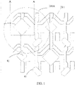
FIG. 1 is a top view illustrating a display panel according to one embodiment of the present application. -
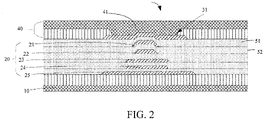
FIG. 2 is a cross-sectional view taken along line A-A ofFIG. 1 illustrating the display panel. -
FIG. 3 is a partially enlarged perspective view of the display panel ofFIG. 1 . -
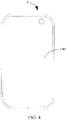
FIG. 4 is a planar view illustrating the display panel according to one embodiment of the present application. - The technical solutions of the present application will be clearly and completely described below with reference to the accompanying drawings and specific embodiments of the present application. Obviously, the described embodiments are only some of the embodiments of the present application, and not all of the embodiments. Based on the embodiments in the present application, all other embodiments obtained by those skilled in the art without inventiveness fall into the protection scope of the present application.
- Please refer to
FIG. 1 andFIG. 2 , which illustrate adisplay panel 100 according to a first embodiment of the present application. In the present embodiment, an organic light emitting diode (OLED) display panel is used as an example. However, thedisplay panel 100 of the present application can also be other types of display panels, such as quantum dot light-emitting diode (QLED) display panels, micro-LED display panels, and Mini-LED display panels. - The
display panel 100 comprises asubstrate 10, adriving circuit layer 20 disposed on thesubstrate 10, a pixel definition layer 30 disposed on thedriving circuit layer 20, and a light-emitting layer 40 disposed on thedriving circuit layer 20 and arranged in the pixel definition layer 30. - The
substrate 10 is a transparent substrate, which can be made of a hard material such as glass or quartz, or made of a flexible material such as a plastic thin film or paper fibers. A light shielding layer, a buffer layer, and etc. can be disposed between thesubstrate 10 and thedriving circuit layer 20. - The
driving circuit layer 20 comprises afirst metal layer 21, asecond metal layer 22, athird metal layer 23, afourth metal layer 24, and asemiconductor layer 25. Thesemiconductor layer 25, thefourth metal layer 24, thethird metal layer 23, thesecond metal layer 22, and thefirst metal layer 21 are sequentially stacked on thesubstrate 10. Two adjacent layers are electrically insulated and separated from each other by an insulating layer. Thedriving circuit layer 20 can comprise a plurality of thin film transistors (TFTs) and capacitors. For example, it can be a two-transistor and one-capacitor (2T1C) driving circuit, 3T1C circuit, 7T1C circuit, or etc. - Please refer to
FIG. 2 . The first metal layer is a first source/drain layer. Thefirst metal layer 21 comprises afirst metal trace 211. - The
second metal layer 22 is a second source/drain layer. Thesecond metal layer 22 comprises a second metal trace 221. - According to one embodiment of the present application, the
first metal layer 21 is made of a titanium-aluminum-titanium laminate. Thesecond metal layer 22 is also made of a titanium-aluminum-titanium laminate. - The
third metal layer 23 is a first gate metal layer. - The
fourth metal layer 24 is a second gate metal layer. - The
semiconductor layer 25 is an active layer of the TFT. Thesemiconductor layer 25 can be made of amorphous silicon, single-crystal silicon, polysilicon, or an oxide semiconductor material such as indium gallium zinc oxide (IGZO). - A plurality of
openings 31 are defined in the pixel definition layer 30, and theopenings 31 are used for arranging the light-emittinglayer 40 therein. - The light-
emitting layer 40 comprises an anode layer disposed on thedriving circuit layer 20, and a hole injection layer, a hole transport layer, an electron transport layer, an organic light-emitting material layer, an electron injection layer, and a cathode layer which are sequentially stacked on the anode layer. It is apparent that the light-emittinglayer 40 in the present application can comprise only a cathode layer, a light emission layer, and the anode layer, and can further comprise one or more of the electron injection layer, the electron transport layer, an electron blocking layer, the hole injection layer, the hole transport layer, a hole blocking layer, and a charge generation layer. - The light-emitting
layer 40 comprises a plurality of light-emittingportions 41. The light-emittingportion 41 can be one or more of a red sub-light-emitting portion, a blue sub-light-emitting portion, and a green sub-light-emitting portion for display functions. It can be understood that the light-emittingportion 41 can also include sub-light-emitting portions of other colors. Afirst passivation layer 51 is disposed between thefirst metal layer 21 and the light-emittinglayer 40. A vertical distance d between an orthographic projection o of a geometric center of each light-emittingportion 41 projected on thefirst metal layer 21 and a symmetry axis S of thefirst metal trace 211 is less than or equal to 5 µm, Please refer toFIG. 3 again.FIG. 3 is an enlarged perspective view of aregion 100A of the display panel ofFIG. 1 . A shape of thefirst metal layer 21 located below the light-emittinglayer 40 is drawn with a dashed line inFIG. 3 . When thefirst metal trace 211 is not of uniform width, the symmetry axis S of thefirst metal trace 211 refers to a symmetry axis along the length direction at a position where the orthographic projection o of the geometric center of the light-emittingportion 41 overlaps with thefirst metal layer 21. That is the symmetry axis of thefirst metal trace 211 in a region right under the geometric center of the light-emittingportion 41, and the symmetry axis is parallel to an extending direction of thefirst metal trace 211. The symmetry axis S is obtained by, for example, creating a line segment starting from the orthographic projection o on thefirst metal layer 21 projected by the geometric center of the light emitting portion 41and perpendicular to the extending direction of thefirst metal trace 211, then finding a midpoint of the line segment and creating a straight line passing through the midpoint A and parallel to the extending direction of thefirst metal trace 211 to be the symmetry axis S. The vertical distance d between the orthographic projection o of the geometric center of each light-emittingportion 41 projected on thefirst metal layer 21 and the symmetry axis S of thefirst metal trace 211 means that, by creating a vertical line starting from the orthographic projection o of the geometric center on thefirst metal layer 21 and perpendicular to the symmetry axis S, the distance is from the orthographic projection o to an intersection of the vertical line and the symmetry axis S. - According to one embodiment of the present application, the vertical distance d between the orthographic projection o of the geometric center of each light-emitting
portion 41 projected on thefirst metal layer 21 and the symmetry axis S of thefirst metal trace 211 is less than or equal to 2 µm. - According to another embodiment of the present application, the orthographic projection of the geometric center of each light-emitting
portion 41 projected on thefirst metal layer 21 overlaps with the symmetry axis S of thefirst metal trace 211. - Since a metal thickness of the
first metal layer 21 is greater, it is difficult to obtain a flat surface even though thefirst passivation layer 51 is disposed on thefirst metal layer 21. When the light-emittingportion 41 is further disposed on thefirst passivation layer 51, the geometric center of the light-emittingportion 41 is arranged as close as possible to the symmetry axis S of thefirst metal trace 211. Therefore, when a user is watching a display screen from left and right sides of thedisplay panel 100, color shits are basically symmetrical while viewed from the viewing angles on two sides, thus improving the asymmetry viewed from the left and right viewing angles, and improving display quality. - A
second passivation layer 52 is disposed between thefirst metal layer 21 and thesecond metal layer 22. In one embodiment, the orthographic projection of the light-emittingportion 41 projected on thesecond metal layer 22 overlaps with a projection of a portion of thefirst metal trace 211 projected on thesecond metal layer 22. That is to say, below the light-emittingportion 41, thefirst metal layer 21 and thesecond metal layer 22 just overlap each other. As a result, unevenness of thefirst passivation layer 51 is more obvious. By arranging the geometric center of the light-emittingportion 41 as close as possible to the symmetry axis S of thefirst metal trace 211, the asymmetry viewed from left and right viewing angles can be improved, and display quality can also be improved. - In addition, the above embodiments only show examples of a dual-gate and dual-source/drain configuration, but the technical solution of the present application is not intended to limit the number of gate electrodes and source/drain electrodes. For example, in one embodiment of the present application, the driving
circuit layer 20 can include only the first source/drain layer and the first gate metal layer. Similarly, the distance between the orthographic projection of the geometric center of the light-emittingportion 41 projected on thefirst metal layer 21 and the symmetry axis S of thefirst metal trace 211 is less than or equal to 5 µm. - In the present application, the TFT in the driving circuit layer is not limited to a particular type, and the technical solution of the present application can be used in a top gate TFT array substrate and a bottom gate TFT array substrate.
- Please refer to
FIG. 4 . The present application further provides adisplay device 1 which comprises thedisplay panel 100 described above. - Compared with conventional techniques, the display panel and the display device of the present application arranges the center of the light-emitting portion as close as possible to the symmetry axis of the metal trace located below the light-emitting portion. Such a configuration can improve the asymmetry viewed from left and right viewing angles and improve display quality, even if the passivation layer under the light-emitting portion is not flat enough.
- A detailed description about the embodiments of the present application is provided above. Specific examples are used in the present disclosure to explain the principles and embodiments of the present application. The description of the above embodiments is only for ease of understanding the present application. Those skilled in the art can make changes and modifications to the above embodiments and their use based on the idea of the present application. In summary, the content of the present disclosure should not be construed as a limitation on the present application.
Claims (18)
- A display panel, comprising:a substrate;a driving circuit layer disposed on the substrate; anda light-emitting layer disposed on the driving circuit layer;wherein the driving circuit layer comprises a first metal layer, the first metal layer comprises a first metal trace , the light-emitting layer comprises a plurality of light-emitting portions, and a vertical distance between an orthographic projection of a center of each light-emitting portion projected on the first metal layer and a symmetry axis of the first metal trace is less than or equal to 5 µm.
- The display panel according to claim 1, wherein the vertical distance between the orthographic projection of the center of each light-emitting portion projected on the first metal layer and the symmetry axis of the first metal trace is less than or equal to 2 µm.
- The display panel according to claim 1, wherein the orthographic projection of the center of each light-emitting portion projected on the first metal layer overlaps with the symmetry axis of the first metal trace.
- The display panel according to claim 1, wherein a first passivation layer is disposed between the first metal layer and the light-emitting layer.
- The display panel according to claim 1, wherein the driving circuit layer further comprises a second metal layer, the second metal layer comprises a second metal trace, the second metal layer is disposed between the first metal layer and the substrate, and a second passivation layer is disposed between the first metal layer and the second metal layer.
- The display panel according to claim 1, wherein the first metal layer is a first source/drain layer.
- The display panel according to claim 5, wherein the second metal layer is a second source/drain layer.
- The display panel according to claim 5, wherein an orthographic projection of the light-emitting portion projected on the second metal layer overlaps with an orthographic projection of a portion of the first metal trace projected on the second metal layer.
- The display panel according to claim 1, wherein the first metal layer is made of a titanium-aluminum-titanium laminate.
- A display device, comprising the display panel of claim 1.
- The display device according to claim 10, wherein the vertical distance between the orthographic projection of the center of each light-emitting portion projected on the first metal layer and the symmetry axis of the first metal trace is less than or equal to 2 µm.
- The display device according to claim 10, wherein the orthographic projection of the center of each light-emitting portion projected on the first metal layer overlaps with the symmetry axis of the first metal trace.
- The display device according to claim 10, wherein a first passivation layer is disposed between the first metal layer and the light-emitting layer.
- The display device according to claim 10, wherein the driving circuit layer further comprises a second metal layer, the second metal layer comprises a second metal trace, the second metal layer is disposed between the first metal layer and the substrate, and a second passivation layer is disposed between the first metal layer and the second metal layer.
- The display device according to claim 10, wherein the first metal layer is a first source/drain layer.
- The display device according to claim 10, wherein the second metal layer is a second source/drain layer.
- The display device according to claim 14, wherein an orthographic projection of the light-emitting portion projected on the second metal layer overlaps with an orthographic projection of a portion of the first metal trace projected on the second metal layer.
- The display device according to claim 14, wherein the first metal layer is made of a titanium-aluminum-titanium laminate.
Applications Claiming Priority (2)
| Application Number | Priority Date | Filing Date | Title |
|---|---|---|---|
| CN202010150019.XA CN111341809A (en) | 2020-03-06 | 2020-03-06 | Display panel and display device |
| PCT/CN2020/080777 WO2021174604A1 (en) | 2020-03-06 | 2020-03-24 | Display panel and display device |
Publications (2)
| Publication Number | Publication Date |
|---|---|
| EP4117039A1 true EP4117039A1 (en) | 2023-01-11 |
| EP4117039A4 EP4117039A4 (en) | 2024-04-17 |
Family
ID=71187865
Family Applications (1)
| Application Number | Title | Priority Date | Filing Date |
|---|---|---|---|
| EP20730959.2A Pending EP4117039A4 (en) | 2020-03-06 | 2020-03-24 | DISPLAY BOARD AND DISPLAY DEVICE |
Country Status (4)
| Country | Link |
|---|---|
| US (1) | US11557639B2 (en) |
| EP (1) | EP4117039A4 (en) |
| CN (1) | CN111341809A (en) |
| WO (1) | WO2021174604A1 (en) |
Families Citing this family (1)
| Publication number | Priority date | Publication date | Assignee | Title |
|---|---|---|---|---|
| CN115988929A (en) * | 2020-10-16 | 2023-04-18 | 京东方科技集团股份有限公司 | display panel, display device |
Family Cites Families (20)
| Publication number | Priority date | Publication date | Assignee | Title |
|---|---|---|---|---|
| US9153171B2 (en) * | 2012-12-17 | 2015-10-06 | LuxVue Technology Corporation | Smart pixel lighting and display microcontroller |
| KR101560272B1 (en) * | 2013-02-25 | 2015-10-15 | 삼성디스플레이 주식회사 | Organic light emitting display device and manufacturing method of the same |
| JP2015187635A (en) * | 2014-03-26 | 2015-10-29 | 株式会社Joled | Color variation member, light-emitting device, display device, and electronic apparatus |
| CN104466007B (en) * | 2014-12-30 | 2017-05-03 | 京东方科技集团股份有限公司 | Pixel structure, display method of pixel structure and display device |
| CN205091725U (en) * | 2015-01-29 | 2016-03-16 | 阿尔卑斯电气株式会社 | Input apparatus |
| CN107644888B (en) * | 2016-07-22 | 2025-01-10 | 京东方科技集团股份有限公司 | Pixel arrangement structure, display substrate, display device, manufacturing method and mask |
| US11264430B2 (en) * | 2016-02-18 | 2022-03-01 | Chengdu Boe Optoelectronics Technology Co., Ltd. | Pixel arrangement structure with misaligned repeating units, display substrate, display apparatus and method of fabrication thereof |
| KR102688600B1 (en) * | 2016-05-03 | 2024-07-25 | 삼성디스플레이 주식회사 | Organic light emitting display |
| KR102717868B1 (en) | 2016-09-13 | 2024-10-15 | 삼성디스플레이 주식회사 | Display device |
| KR102750040B1 (en) * | 2016-12-01 | 2025-01-03 | 삼성디스플레이 주식회사 | Organic light emitting display device and manufacturing method thereof |
| CN108155205B (en) * | 2016-12-02 | 2020-09-11 | 信利(惠州)智能显示有限公司 | AMOLED display |
| KR102404266B1 (en) * | 2017-08-31 | 2022-05-30 | 엘지디스플레이 주식회사 | Electroluminescence display |
| JP7079106B2 (en) * | 2018-01-24 | 2022-06-01 | シャープ株式会社 | Image display element and manufacturing method of image display element |
| KR102556020B1 (en) * | 2018-01-31 | 2023-07-17 | 삼성디스플레이 주식회사 | Thin film transistor array substrate and organic light emitting diode display |
| CN109037282B (en) * | 2018-07-24 | 2021-10-22 | 京东方科技集团股份有限公司 | Array substrate and manufacturing method thereof, display panel and display device |
| EP3667720B1 (en) * | 2018-12-10 | 2022-09-21 | IMEC vzw | Apex angle reduction in a led device with a led array |
| WO2020176783A1 (en) * | 2019-02-28 | 2020-09-03 | Magic Leap, Inc. | Display system and method for providing variable accommodation cues using multiple intra-pupil parallax views formed by light emitter arrays |
| CN109786434B (en) * | 2019-03-28 | 2022-04-22 | 京东方科技集团股份有限公司 | Array substrate, preparation method thereof, display panel, device and pixel driving circuit |
| CN110265460A (en) * | 2019-06-27 | 2019-09-20 | 京东方科技集团股份有限公司 | OLED display substrate, manufacturing method thereof, and display device |
| CN110610980B (en) * | 2019-10-23 | 2022-06-03 | 京东方科技集团股份有限公司 | Display substrate, preparation method thereof and display device |
-
2020
- 2020-03-06 CN CN202010150019.XA patent/CN111341809A/en active Pending
- 2020-03-24 WO PCT/CN2020/080777 patent/WO2021174604A1/en not_active Ceased
- 2020-03-24 EP EP20730959.2A patent/EP4117039A4/en active Pending
- 2020-03-24 US US16/758,056 patent/US11557639B2/en active Active
Also Published As
| Publication number | Publication date |
|---|---|
| US11557639B2 (en) | 2023-01-17 |
| WO2021174604A9 (en) | 2022-09-15 |
| WO2021174604A1 (en) | 2021-09-10 |
| US20220045154A1 (en) | 2022-02-10 |
| EP4117039A4 (en) | 2024-04-17 |
| CN111341809A (en) | 2020-06-26 |
Similar Documents
| Publication | Publication Date | Title |
|---|---|---|
| US12238974B2 (en) | Display substrate and method for manufacturing the same, display panel, and display apparatus | |
| US7164230B2 (en) | Dual panel-type organic electroluminescent display device and method for fabricating the same | |
| US12108631B2 (en) | Display device | |
| CN112117306B (en) | Display device | |
| US11785821B2 (en) | Display substrate and related device | |
| US11024686B2 (en) | OLED pixel structure and OLED display panel | |
| US20220005890A1 (en) | An array substrate, a method for manufacturing the same, and a display device | |
| CN106981520A (en) | Thin film transistor (TFT) and preparation method thereof, array base palte and display device | |
| CN113066841B (en) | Display substrate and manufacturing method thereof | |
| US8618547B2 (en) | Mask assembly and organic light emitting diode display manufactured using the same | |
| US9680122B1 (en) | Organic light emitting display device and method of manufacturing the same | |
| WO2018205652A1 (en) | Pixel structure and manufacturing method therefor, and display substrate and display apparatus | |
| US12477917B2 (en) | Display substrate and related devices with improved resolution | |
| CN115428162B (en) | Display panel and manufacturing method thereof, and display device | |
| US20250248240A1 (en) | Display panel, manufacturing method therefor, and display apparatus | |
| KR101663743B1 (en) | Organic Electroluminescent Display Device | |
| US12604605B2 (en) | Display substrate, method for manufacturing display substrate, method for driving display substrate, display panel and display device | |
| US11557639B2 (en) | Display panel and display device with light-emitting portions having centers at distance of 5μm or less | |
| TWI860812B (en) | Organic light emitting diode display device and method of fabricating the same | |
| WO2020113661A1 (en) | Display panel | |
| KR101096719B1 (en) | Organic Electroluminescence Display Device And Method For Fabricating The Same | |
| US20250107393A1 (en) | Display Panel and Manufacturing Method Therefor, and Display Device | |
| KR101957144B1 (en) | Array substrate | |
| US12389755B2 (en) | Display device | |
| CN118866976A (en) | A thin film transistor and its manufacturing method, substrate and display device |
Legal Events
| Date | Code | Title | Description |
|---|---|---|---|
| STAA | Information on the status of an ep patent application or granted ep patent |
Free format text: STATUS: UNKNOWN |
|
| STAA | Information on the status of an ep patent application or granted ep patent |
Free format text: STATUS: THE INTERNATIONAL PUBLICATION HAS BEEN MADE |
|
| PUAI | Public reference made under article 153(3) epc to a published international application that has entered the european phase |
Free format text: ORIGINAL CODE: 0009012 |
|
| STAA | Information on the status of an ep patent application or granted ep patent |
Free format text: STATUS: REQUEST FOR EXAMINATION WAS MADE |
|
| 17P | Request for examination filed |
Effective date: 20200616 |
|
| AK | Designated contracting states |
Kind code of ref document: A1 Designated state(s): AL AT BE BG CH CY CZ DE DK EE ES FI FR GB GR HR HU IE IS IT LI LT LU LV MC MK MT NL NO PL PT RO RS SE SI SK SM TR |
|
| DAV | Request for validation of the european patent (deleted) | ||
| DAX | Request for extension of the european patent (deleted) | ||
| REG | Reference to a national code |
Ref country code: DE Ref legal event code: R079 Free format text: PREVIOUS MAIN CLASS: H01L0027320000 Ipc: H10K0059800000 |
|
| A4 | Supplementary search report drawn up and despatched |
Effective date: 20240319 |
|
| RIC1 | Information provided on ipc code assigned before grant |
Ipc: H10K 59/80 20230101AFI20240313BHEP |