EP3667720B1 - Apex angle reduction in a led device with a led array - Google Patents
Apex angle reduction in a led device with a led array Download PDFInfo
- Publication number
- EP3667720B1 EP3667720B1 EP18211303.5A EP18211303A EP3667720B1 EP 3667720 B1 EP3667720 B1 EP 3667720B1 EP 18211303 A EP18211303 A EP 18211303A EP 3667720 B1 EP3667720 B1 EP 3667720B1
- Authority
- EP
- European Patent Office
- Prior art keywords
- led
- conductive structure
- light
- leds
- led device
- Prior art date
- Legal status (The legal status is an assumption and is not a legal conclusion. Google has not performed a legal analysis and makes no representation as to the accuracy of the status listed.)
- Active
Links
- 230000009467 reduction Effects 0.000 title description 5
- 238000000034 method Methods 0.000 claims description 33
- 230000008569 process Effects 0.000 claims description 21
- 239000000463 material Substances 0.000 claims description 7
- OKTJSMMVPCPJKN-UHFFFAOYSA-N Carbon Chemical compound [C] OKTJSMMVPCPJKN-UHFFFAOYSA-N 0.000 claims description 5
- 229910052799 carbon Inorganic materials 0.000 claims description 5
- 239000003989 dielectric material Substances 0.000 claims description 4
- RYGMFSIKBFXOCR-UHFFFAOYSA-N Copper Chemical group [Cu] RYGMFSIKBFXOCR-UHFFFAOYSA-N 0.000 claims description 3
- 239000004065 semiconductor Substances 0.000 claims description 2
- 230000000295 complement effect Effects 0.000 claims 1
- 239000010410 layer Substances 0.000 description 22
- 230000003287 optical effect Effects 0.000 description 15
- 239000011295 pitch Substances 0.000 description 14
- 238000009826 distribution Methods 0.000 description 6
- 239000010949 copper Substances 0.000 description 5
- VYPSYNLAJGMNEJ-UHFFFAOYSA-N Silicium dioxide Chemical compound O=[Si]=O VYPSYNLAJGMNEJ-UHFFFAOYSA-N 0.000 description 4
- 238000000231 atomic layer deposition Methods 0.000 description 4
- PNEYBMLMFCGWSK-UHFFFAOYSA-N aluminium oxide Inorganic materials [O-2].[O-2].[O-2].[Al+3].[Al+3] PNEYBMLMFCGWSK-UHFFFAOYSA-N 0.000 description 3
- 229910052593 corundum Inorganic materials 0.000 description 3
- 238000004519 manufacturing process Methods 0.000 description 3
- 229910001845 yogo sapphire Inorganic materials 0.000 description 3
- GWEVSGVZZGPLCZ-UHFFFAOYSA-N Titan oxide Chemical compound O=[Ti]=O GWEVSGVZZGPLCZ-UHFFFAOYSA-N 0.000 description 2
- 230000003667 anti-reflective effect Effects 0.000 description 2
- 238000003491 array Methods 0.000 description 2
- 230000008901 benefit Effects 0.000 description 2
- 229910052681 coesite Inorganic materials 0.000 description 2
- 229910052906 cristobalite Inorganic materials 0.000 description 2
- 239000000377 silicon dioxide Substances 0.000 description 2
- 229910052682 stishovite Inorganic materials 0.000 description 2
- 229910052905 tridymite Inorganic materials 0.000 description 2
- KJTLSVCANCCWHF-UHFFFAOYSA-N Ruthenium Chemical compound [Ru] KJTLSVCANCCWHF-UHFFFAOYSA-N 0.000 description 1
- 239000006117 anti-reflective coating Substances 0.000 description 1
- 230000003190 augmentative effect Effects 0.000 description 1
- 230000009286 beneficial effect Effects 0.000 description 1
- 230000008859 change Effects 0.000 description 1
- 239000004020 conductor Substances 0.000 description 1
- 229910052802 copper Inorganic materials 0.000 description 1
- 230000008878 coupling Effects 0.000 description 1
- 238000010168 coupling process Methods 0.000 description 1
- 238000005859 coupling reaction Methods 0.000 description 1
- 230000001419 dependent effect Effects 0.000 description 1
- 239000002355 dual-layer Substances 0.000 description 1
- 230000005670 electromagnetic radiation Effects 0.000 description 1
- 239000011521 glass Substances 0.000 description 1
- AMGQUBHHOARCQH-UHFFFAOYSA-N indium;oxotin Chemical compound [In].[Sn]=O AMGQUBHHOARCQH-UHFFFAOYSA-N 0.000 description 1
- 230000010354 integration Effects 0.000 description 1
- 239000011159 matrix material Substances 0.000 description 1
- 238000001465 metallisation Methods 0.000 description 1
- 238000000623 plasma-assisted chemical vapour deposition Methods 0.000 description 1
- 229920000642 polymer Polymers 0.000 description 1
- 238000005215 recombination Methods 0.000 description 1
- 230000006798 recombination Effects 0.000 description 1
- 229910052707 ruthenium Inorganic materials 0.000 description 1
- 235000012239 silicon dioxide Nutrition 0.000 description 1
- 239000002356 single layer Substances 0.000 description 1
- 239000000758 substrate Substances 0.000 description 1
- OGIDPMRJRNCKJF-UHFFFAOYSA-N titanium oxide Inorganic materials [Ti]=O OGIDPMRJRNCKJF-UHFFFAOYSA-N 0.000 description 1
- 239000012780 transparent material Substances 0.000 description 1
- WFKWXMTUELFFGS-UHFFFAOYSA-N tungsten Chemical compound [W] WFKWXMTUELFFGS-UHFFFAOYSA-N 0.000 description 1
- 229910052721 tungsten Inorganic materials 0.000 description 1
- 239000010937 tungsten Substances 0.000 description 1
Images


Classifications
-
- H—ELECTRICITY
- H01—ELECTRIC ELEMENTS
- H01L—SEMICONDUCTOR DEVICES NOT COVERED BY CLASS H10
- H01L25/00—Assemblies consisting of a plurality of individual semiconductor or other solid state devices ; Multistep manufacturing processes thereof
- H01L25/03—Assemblies consisting of a plurality of individual semiconductor or other solid state devices ; Multistep manufacturing processes thereof all the devices being of a type provided for in the same subgroup of groups H01L27/00 - H01L33/00, or in a single subclass of H10K, H10N, e.g. assemblies of rectifier diodes
- H01L25/04—Assemblies consisting of a plurality of individual semiconductor or other solid state devices ; Multistep manufacturing processes thereof all the devices being of a type provided for in the same subgroup of groups H01L27/00 - H01L33/00, or in a single subclass of H10K, H10N, e.g. assemblies of rectifier diodes the devices not having separate containers
- H01L25/075—Assemblies consisting of a plurality of individual semiconductor or other solid state devices ; Multistep manufacturing processes thereof all the devices being of a type provided for in the same subgroup of groups H01L27/00 - H01L33/00, or in a single subclass of H10K, H10N, e.g. assemblies of rectifier diodes the devices not having separate containers the devices being of a type provided for in group H01L33/00
- H01L25/0753—Assemblies consisting of a plurality of individual semiconductor or other solid state devices ; Multistep manufacturing processes thereof all the devices being of a type provided for in the same subgroup of groups H01L27/00 - H01L33/00, or in a single subclass of H10K, H10N, e.g. assemblies of rectifier diodes the devices not having separate containers the devices being of a type provided for in group H01L33/00 the devices being arranged next to each other
-
- H—ELECTRICITY
- H01—ELECTRIC ELEMENTS
- H01L—SEMICONDUCTOR DEVICES NOT COVERED BY CLASS H10
- H01L27/00—Devices consisting of a plurality of semiconductor or other solid-state components formed in or on a common substrate
- H01L27/15—Devices consisting of a plurality of semiconductor or other solid-state components formed in or on a common substrate including semiconductor components with at least one potential-jump barrier or surface barrier specially adapted for light emission
- H01L27/153—Devices consisting of a plurality of semiconductor or other solid-state components formed in or on a common substrate including semiconductor components with at least one potential-jump barrier or surface barrier specially adapted for light emission in a repetitive configuration, e.g. LED bars
- H01L27/156—Devices consisting of a plurality of semiconductor or other solid-state components formed in or on a common substrate including semiconductor components with at least one potential-jump barrier or surface barrier specially adapted for light emission in a repetitive configuration, e.g. LED bars two-dimensional arrays
-
- H—ELECTRICITY
- H01—ELECTRIC ELEMENTS
- H01L—SEMICONDUCTOR DEVICES NOT COVERED BY CLASS H10
- H01L25/00—Assemblies consisting of a plurality of individual semiconductor or other solid state devices ; Multistep manufacturing processes thereof
- H01L25/16—Assemblies consisting of a plurality of individual semiconductor or other solid state devices ; Multistep manufacturing processes thereof the devices being of types provided for in two or more different main groups of groups H01L27/00 - H01L33/00, or in a single subclass of H10K, H10N, e.g. forming hybrid circuits
- H01L25/167—Assemblies consisting of a plurality of individual semiconductor or other solid state devices ; Multistep manufacturing processes thereof the devices being of types provided for in two or more different main groups of groups H01L27/00 - H01L33/00, or in a single subclass of H10K, H10N, e.g. forming hybrid circuits comprising optoelectronic devices, e.g. LED, photodiodes
-
- H—ELECTRICITY
- H01—ELECTRIC ELEMENTS
- H01L—SEMICONDUCTOR DEVICES NOT COVERED BY CLASS H10
- H01L2933/00—Details relating to devices covered by the group H01L33/00 but not provided for in its subgroups
- H01L2933/0008—Processes
- H01L2933/0033—Processes relating to semiconductor body packages
- H01L2933/0058—Processes relating to semiconductor body packages relating to optical field-shaping elements
-
- H—ELECTRICITY
- H01—ELECTRIC ELEMENTS
- H01L—SEMICONDUCTOR DEVICES NOT COVERED BY CLASS H10
- H01L2933/00—Details relating to devices covered by the group H01L33/00 but not provided for in its subgroups
- H01L2933/0008—Processes
- H01L2933/0033—Processes relating to semiconductor body packages
- H01L2933/0066—Processes relating to semiconductor body packages relating to arrangements for conducting electric current to or from the semiconductor body
-
- H—ELECTRICITY
- H01—ELECTRIC ELEMENTS
- H01L—SEMICONDUCTOR DEVICES NOT COVERED BY CLASS H10
- H01L33/00—Semiconductor devices with at least one potential-jump barrier or surface barrier specially adapted for light emission; Processes or apparatus specially adapted for the manufacture or treatment thereof or of parts thereof; Details thereof
- H01L33/36—Semiconductor devices with at least one potential-jump barrier or surface barrier specially adapted for light emission; Processes or apparatus specially adapted for the manufacture or treatment thereof or of parts thereof; Details thereof characterised by the electrodes
- H01L33/40—Materials therefor
- H01L33/42—Transparent materials
-
- H—ELECTRICITY
- H01—ELECTRIC ELEMENTS
- H01L—SEMICONDUCTOR DEVICES NOT COVERED BY CLASS H10
- H01L33/00—Semiconductor devices with at least one potential-jump barrier or surface barrier specially adapted for light emission; Processes or apparatus specially adapted for the manufacture or treatment thereof or of parts thereof; Details thereof
- H01L33/48—Semiconductor devices with at least one potential-jump barrier or surface barrier specially adapted for light emission; Processes or apparatus specially adapted for the manufacture or treatment thereof or of parts thereof; Details thereof characterised by the semiconductor body packages
- H01L33/58—Optical field-shaping elements
-
- H—ELECTRICITY
- H01—ELECTRIC ELEMENTS
- H01L—SEMICONDUCTOR DEVICES NOT COVERED BY CLASS H10
- H01L33/00—Semiconductor devices with at least one potential-jump barrier or surface barrier specially adapted for light emission; Processes or apparatus specially adapted for the manufacture or treatment thereof or of parts thereof; Details thereof
- H01L33/48—Semiconductor devices with at least one potential-jump barrier or surface barrier specially adapted for light emission; Processes or apparatus specially adapted for the manufacture or treatment thereof or of parts thereof; Details thereof characterised by the semiconductor body packages
- H01L33/62—Arrangements for conducting electric current to or from the semiconductor body, e.g. lead-frames, wire-bonds or solder balls
Definitions
- the present invention relates to the technical field of Light Emitting Diode (LED) devices, particularly of micro-LED ( ⁇ LED) devices.
- the invention presents an LED device with an LED array, particularly with a ⁇ LED array having a LED pixel pitch in the ⁇ m range. An emission angle of the light provided by the LED device is reduced compared to an emission angle of the light output from the LED array.
- the LED device of the invention is well applicable to ⁇ LED displays as, for instance, used in augmented reality (AR) glasses.
- AR augmented reality
- the emission angle (also referred to as the "beam angle” or “APEX angle”) of light emitted by a light source - e.g. a LED device or array - is the opening angle of the emitted "light beam” or “light cone".
- the emission angle is particularly defined as the angle between the two emission directions, for which the luminous intensity is reduced to 50% of the luminous intensity along a main emission axis/direction of the light source.
- the emission angle is thus twice a certain angle with respect to the main emission axis (also referred to as the "optical axis"), at which the luminous intensity is reduced to 50% of the luminous intensity along the main emission axis.
- the main emission axis is the direction, into which the light source emits the highest relative luminous intensity.
- the emission angle of light emitted by a conventional ⁇ LED array in a LED device is typically between 110-160°. Outside of this rather wide emission angle, the light intensity is significantly reduced or lost, e.g. due to internal reflections.
- the emission angle of the light it emits should be much narrower than the above-mentioned emission angle of the conventional ⁇ LED array.
- the light emission angle of such a LED device should ideally be around 50° or less, in order to allow collimation of the emitted light into, for example, a waveguide.
- a diaphragm or optical lens could be used to collimate the light.
- the design of a diaphragm or lens for such a LED device is very challenging. As of now, no satisfying solution for a LED device with a LED array is available.
- Another challenge for a LED device including a conventional ⁇ LED array is that the smaller the LED pixel pitch is or becomes, the more difficult it is to provide for an efficient current and heat distribution in the device.
- US 2015/362165 A1 discloses a light engine array comprising multiple light engines, and a dam array comprising multiple dams located on a surface of the light engines.
- US 2017/294424 A1 discloses a display apparatus comprising LEDs, and a method of manufacturing the same.
- EP 3 410 479 A1 discloses a display device comprising light-emitting elements on a substrate.
- embodiments of the present invention aim to improve conventional LED devices with LED arrays, particularly with ⁇ LED arrays, and their fabrication process.
- An objective thereby is to provide a LED device, which emits light with a narrow emission angle.
- the emission angle should be narrow enough to allow for an efficient collimation and coupling of the light into, for instance, a waveguide.
- the emission angle of the LED device should especially be well below the emission angle of a conventional ⁇ LED array.
- the above objective should be achieved even for very small LED pixel pitches, i.e. in the low ⁇ m range.
- an efficient heat and current distribution should also be provided in the LED device, particularly in its LED array. Another goal is to fabricate the LED device very compactly, and with an efficient fabrication process that allows reaching high yields.
- a first aspect of the invention relates to a LED device, comprising: a LED array including a plurality of LEDs, at least one top contact and bottom contact electrically connected to the LED array, and a conductive structure arranged above the LED array and the top contact, respectively, and electrically connected to the top contact, wherein the conductive structure is, regarding each LED, configured to absorb a first part of the light emitted by the LED, and to pass a second part of the light emitted by the LED, wherein an emission angle of the passed light is smaller than an emission angle of the light emitted by the LED, and wherein the LED device is characterized by further comprising: a plurality of lenses arranged between the LED array and the conductive structure, wherein each lens is configured to focus at least some of the light emitted by one of the plurality of LEDs, so that the focused light is passed by the conductive structure.
- the conductive structure is configured like this with respect to each single LED in the LED array.
- An emission angle of the passed light being smaller than an emission angle of the light emitted by the LED means the same as that the conductive structure is configured to pass the light emitted by the LED as a collimate beam.
- the conductive structure is configured to absorb the first part of the LED light by having an absorptive surface or at least an absorptive surface region arranged in the light path.
- the conductive structure is further configured to pass the second part of the LED light by having an opening arranged above the LED and transparent at least to the light emitted by the LED.
- the conductive structure is particularly arranged such with respect to the LED beneath it, that the beam angle of the light passing through the opening is narrowed compared to the beam angle of the LED light. That is, the conductive structure serves as a diaphragm. This may be achieved by properly designing the width and height of the conductive structure, and the width or diameter of the openings in the conductive structure.
- Each LED of the LED array is configured to emit light along a certain main emission axis and with a certain emission angle (which is symmetrically around the main emission axis). That is, each LED is configured to output a light beam or light cone with the emission angle being its (APEX) opening angle.
- the emission angle of each LED, and thus also of the LED array as a whole may be between 110-160° (i.e. before the conductive structure and without any optical elements acting on the light).
- the conductive structure absorbs LED light that impinges on it (first part), while it lets the remaining LED light (second part) pass through. Because the LED light has a smaller beam angle after passing the conductive structure than before passing it, an APEX reduction of the emitted light is achieved in the LED device.
- the emission angle of the passed light may be the emission angle of the light output by the LED device as a whole, if the passed light is not affected anymore by any further optical element of the LED device.
- the conductive structure advantageously has a twofold purpose in the LED device. On the one hand, it serves as the diaphragm arranged above the LED array, as described above. On the other hand, since it is electrically connected to the at least one top contact, it can be used to provide a current or voltage to the LED array. In particular, it thus enables an efficient current distribution. Furthermore, it also provides for an efficient heat distribution during operation of the LED device.
- the LED device of the first aspect is particularly suited for being used in a top emission ⁇ LED display.
- each of the lenses focuses at least some light of the LED, which the conductive structure would otherwise be arranged and configured to absorb, i.e. without the lens being present. While the emission angle of the passed light, i.e. after the conductive structure, may still be defined primarily by the dimensions and the arrangement of the conductive structure with respect to the LED - and not by the lens arranged regarding this LED between the LED array and the conductive structure - the total intensity of the passed light may be increased.
- the lenses may be microlenses, reflow lenses, and/or refractive lenses. The lenses are arranged below the conductive structure, but above the LED array and top contact, respectively. However, the lenses may also be arranged above a lower end of the conductive structure but below an upper end of the conductive structure, i.e. within the height of the conductive structure.
- the lenses may, according to an example not forming part of the claimed invention, be diffractive lenses, in which case the lenses do not focus but widen the light coming from the LEDs.
- the conductive structure may be configured to reflect at least some of the widened light such that it passes the conductive structure.
- the conductive structure may be provided with a reflective surface at least in determined surface regions.
- the main emission axis (optical axis) of each LED of the LED device is the axis, into which that LED emits the highest relative luminous intensity.
- This optical axis maybe perpendicular to the LED surface, the LED layers and/or particularly to an active area, e.g. a quantum well layer, of the LED.
- the LED also emits light into directions deviating from the main emission axis, however, at lower relative luminous intensity.
- the luminous intensity of the emitted light drops to 50%.
- the two certain angles determine the emission angle (beam angle) of the light emitted by the LED, namely the emission angle of the light emitted by the LED is the sum of these certain angles (and is twice the same certain angle for a rotational symmetric beam.
- the emission angle (beam angle) of the passed light may be determined likewise. That is, the light of a certain LED passes the conductive structure with a certain main emission axis, in which the passed light has the highest relative luminous intensity. This main emission axis of the passed light typically, but not necessarily, coincides with the main emission axis of the LED.
- the emission angle of the passed light is defined by the sum of the angles from the main emission axis of the passed light to opposite sides thereof, at which the luminous intensity of the passed light drops to 50%. If the passed light is rotation symmetric the emission angle is twice the same angle from the main emission axis to each side, at which the passed light drops to 50%.
- the at least one top contact electrically contacts the LEDs of the LED array from above.
- each LED may be contacted by a single top contact provided on its top surface.
- a common top contact covers the top surface of multiple LEDs or all LEDs.
- the at least one bottom contact contacts each LED from below.
- each LED may be contacted by one single bottom contact from below.
- the conductive structure and the at least one top contact are separate structures. However, together they may be considered to form a top contact structure in the LED device for contacting the LED array.
- the terms “above” and “below” relate to the orientation of the LEDs and particularly the light emission axis/direction of the LED array. “Above” or “top” is the side where the LED array emits light. “Below” or “bottom” is the opposite side. Any element referred to as being “below” the LEDs or the LED array does thus not interfere with the emitting of the LED light.
- the emission angle of the passed light is an angle of 60° or less, particularly is an angle of 40-50°.
- the emission angle of the LED device becomes narrow enough - even without any further optical elements - to be well coupled into a waveguide or the like. Accordingly, the LED device is well suited for application in a ⁇ LED display.
- the LED device further comprises a plurality of lenses arranged above the conductive structure, wherein each lens is configured to focus the light that is emitted by one of the plurality of LEDs and is passed by the conductive structure.
- the emission angle of the passed light i.e. after the conductive structure, may be larger than described above.
- the emission angle of the passed light may be an angle above 60°, or even an angle above 100°, since the lens provided for each LED above the conductive structure further narrows the beam of the passed light. That is, an emission angle of the focused light is smaller than the emission angle of the passed light.
- the emission angle of the focused light may in this case be the emission angle of the light output by the LED device as a whole, if the light coming from the lenses is not influenced anymore by any further optical element of the LED device.
- the lenses may be microlenses, reflow lenses, and/or refractive lenses.
- the emission angle of the passed light is an angle between 60-100°, as exemplarily described above, the emission angle of the focused light may an angle below 60°, e.g. an angle between 40-50°.
- the dimensions of the conductive structure, which lead to the emission angle reduction regarding each of the LEDs, can be designed larger, thus processing of it becomes simpler.
- the emission angle of the focused light may be an angle below 40°, e.g. an angle between 25-40°. In this way, an even narrower emission angle of the LED device as a whole becomes possible.
- the conductive structure comprises a light-absorbing layer to absorb light emitted by the plurality of LEDs, particularly a carbon layer or a layer of a high refractive index material.
- the light-absorbing layer may be disposed onto the outer surface of a conductive core of the conductive structure, at least onto determined surface regions arranged in the path of LED light that is to be removed. However, also the complete surface of the core of the conductive structure may be coated with such an absorbing layer.
- the conductive structure may be configured to absorb the first part of the light emitted by each LED, in order to reduce the emission angle. For instance, when considering a central point of light emission in the LED active area, i.e. the point in the LED active area through which the optical axis of the LED extends, light emitted from this point at angles below a determined angle may pass the conductive structure, while light emitted from this point above a determined angle may be absorbed by the conductive structure. For the light emitted from this point, the emission angle is thus narrowed.
- a carbon layer is simply very black and is thus absorptive.
- a high refractive index material e.g. ALD Al 2 O 3
- ALD Al 2 O 3 will let light coming from the LED pass (due to the refractive index change), but the light will reflect at the core of the conductive structure and cannot anymore pass the high refractive index material in the opposite direction. Thus, the light enters the layer of the high refractive index material, where it is trapped.
- the LED device further comprises a transparent top contact connected to several or each of the plurality of LEDs and arranged between the LED array and the conductive structure.
- the transparent top contact is a common top contact, common to at least some of the LEDs.
- the top contact is particularly transparent to the LED light.
- the common top contact simplifies the processing of the LED device, and allows designing a smaller LED array with an optimized overall area occupied by LED surface (aperture).
- the conductive structure is connected to determined regions of a top surface of the top contact, the determined regions being positioned above the spaces between adjacent LEDs.
- the determined regions may be only positioned above the spaces between the LEDs, not above the LEDs themselves. Accordingly, the determined regions may be aligned with the spaces when the LED device is viewed in a top view, i.e. from above.
- the conductive structure as a whole is put on the top contact such that it follows the spaces between the multiple LEDs beneath the top contact. In this way, the conductive structure is able to contact the top contact, to serve as a diaphragm for each of the LEDs, and to separate the light coming from different LEDs.
- the conductive structure comprises a plurality of transparent openings, each transparent opening being related to one of the plurality of LEDs.
- each transparent opening may be arranged above the LED it is related to.
- Transparent opening means that the opening is configured to pass at least the light of interest emitted by the LED it is related to.
- the transparent openings can be realized with a transparent material being embedded into cavities of the conductive structure and located above the LEDs.
- the transparent openings may filter electromagnetic radiation other than the light of interest of the LEDs.
- the conductive structure comprises a plurality of vertical posts, the vertical posts being positioned above the spaces between the plurality of LEDs and configured to separate adjacent LEDs from each other.
- the vertical posts are aligned with the contours of the LEDs in a top view of the LED device.
- Each LED may be surrounded by one or more vertical posts, in the top view.
- the vertical posts may have an absorptive surface facing the LEDs, or may at least absorptive regions on that surface. The vertical posts separate adjacent LEDs from each other with respect to the light emitted by each LED being separated.
- an upper surface of the conductive structure defines the transparent openings and is located at a determined distance above the LED array.
- the determined distance and a size (e.g. a width or diameter) of each an opening determines with respect to an LED, how strong the reduction of the emission angle of the passed light is with respect to the light emitted by this LED.
- the LED array has a LED pixel pitch between 1-10 ⁇ m, in particular equal to or below 3 ⁇ m, and/or a height of the conductive structure is between 0.1-1 times, in particular between 0.5-0.8 times, a LED pixel pitch of the LED array.
- the LED array is particularly a ⁇ LED array.
- the LEDs in this array can be placed closely together, thus allowing a very compact LED device but with maximized LED apertures.
- the height of the conductive structure is in the range of the LED pixel pitch, and thus works well as the diaphragm.
- the conductive structure comprises a metallic core, particularly a copper core, and is embedded in a dielectric material.
- the conductive structure may be a damascene-processed structure, i.e. may be produced by using a damascene process.
- this may be a damascene copper (Cu) process and/or a dual-damascene process.
- it can be a tungsten (W) damascene process or ruthenium (Ru) damascene process as well.
- the dielectric is preferably transparent for the LED light.
- the conductive structure can be made in one process step, and can be made such that it serves as a highly conductive metallization grid for efficient current and heat distribution in the LED device, and serves as the diaphragm reducing the emission angle of the LED light.
- the LED device further comprises a plurality of bottom contacts, wherein each bottom contact is electrically connected to one of the plurality of LEDs, and a CMOS IC connected through the bottom contacts to the LEDs and configured to drive the LED array.
- the CMOS IC may also be configured to readout the LED array.
- the CMOS IC may include an active matrix of logical elements, one associated with each LED of the LED array. One bottom contact per LED is provided below the LED array.
- the CMOS IC may be provided directly beneath the bottom contacts, i.e. close to the LED array.
- the LED device is an integrated LED chip or wafer, wherein particularly the LED array, the at least one top and bottom contact and the conductive structure are integrated.
- the LED device can thus be fabricated in a very compact manner and with an efficient process.
- a second aspect of the invention relates to a method for fabricating a LED device, the method comprising: processing a LED array including a plurality of LEDs, processing at least one top contact and bottom contact electrically connected to the LED array, and processing, particularly with a damascene process, a conductive structure arranged above the LED array and the top contact, respectively, and electrically connected to the top contact, wherein the conductive structure is, regarding each LED, configured to absorb a first part of the light emitted by the LED, and to pass a second part of the light emitted by the LED, wherein an emission angle of the passed light is smaller than an emission angle of the light emitted by the LED, and wherein the method is characterized by further comprising: processing a plurality of lenses between the LED array and the conductive structure, wherein each lens is configured to focus at least some of the light emitted by one of the plurality of LEDs, so that the focused light is passed by the conductive structure.
- the conductive structure can either be a single-layer structure or a dual-layer structure (when fabricated in a dual-damascene process), wherein at least one of these layers is configured to absorb the first part of the light, for instance, by being provided with an anti-reflective coating.
- the method of the second aspect may be developed in implementation forms according to the implementation forms described for the LED device of the first aspect.
- FIG. 1 shows a LED device 10 according to an illustrative example not forming part of the invention as claimed.
- the LED device 10 may particularly be a ⁇ LED device, which is suitable for being used in a ⁇ LED display.
- the LED device 10 may be an integrated chip or wafer, e.g. monolithically integrated.
- the LED device comprises a LED array 11, particularly a ⁇ LED array, which includes a plurality of LEDs 12.
- the LEDs 12 of the LED array 11 may, for example, be arranged in rows and/or columns, or in any other two-dimensional pattern.
- An LED pixel pitch i.e. a center-to-center distance between adjacent LEDs 12 (i.e. the sum of LED width/diameter and the space between adjacent LEDs 12) may be in the ⁇ m range, particularly may be equal to or below 3 ⁇ m.
- Each LED 12 of the LED array 11 is configured to emit light, wherein an emission angle 17 of the emitted LED light may be between 110°-160°. That means, each LED 12 can emit light with a certain beam angle 17.
- the emission angle 17 of each LED 12 is preferably similar or equal. Due to the close arrangement of the LEDs 12, an emission angle of the light emitted by the LED array 11 as a whole is the same as the emission angle 17.
- the LED device 10 includes at least one top contact 13 electrically connected to the LED array 11 from above, and at least one bottom contact 14 electrically connected to the LED array from below.
- “Above” and “below” are defined along the main emission axis 18 of each LED 12 (parallel to the vertical direction in FIG. 1 ), wherein it is assumed that the main emission axes 18 of the LEDs 12 are parallel.
- Each LED 12 is contacted by at least one top contact 13 and bottom contact 14, and when a sufficient voltage is applied between these two contacts 13 and 14, the LED 12 emits the light.
- Each LED 12 may have its own top contact 13 and/or its own bottom contact 14, but also common contacts can be applied to several LEDs 12 or even all of the LEDs 12 in the LED array 11.
- the at least one top contact 13 may particularly made of a transparent conductive material, for instance: Indium Tin Oxide (ITO), highly-doped n-GaN, or highly-doped p-GaN.
- ITO Indium Tin Oxide
- the LED pixel pitch equal to or smaller than 3 ⁇ m can be achieved, while the optical apertures of the LEDs 12 can be maximized, i.e. the LED surfaces occupy as much area of the LED array 11 as possible.
- the LED device 10 further comprises a conductive structure 15, which is arranged above the LED array 11 and above the at least one top contact 13, respectively.
- the conductive structure 15 is electrically connected to the top contact 13. Thus, it can be used to provide current to the LED array 11, and also serves as heat distributor during operation of the LEDs 112.
- the conductive structure 15 is provided on the top contact 13, at least on dedicated regions of its top surface, particularly regions of the top surface of the top contact 13, which are positioned above the spaces between adjacent LEDs 12 in the LED array 11 below the top contact 13.
- the conductive structure 15 is further configured to act as a diaphragm for the LED array 11, particularly for each LED 12, in order to narrow the emission angle regarding each LED 12 and thus of the LED array 11 as a whole.
- the conductive structure 15 is dimensioned, arranged and configured, regarding each of the LEDs 12, such that - in operation of the LED device 10 - it absorbs a first part of the light emitted by the LED 12, and passes a second part of light emitted by the LED 12.
- the first part that is absorbed is light emitted by the LED 12 hitting an absorptive surface or surface region of the conductive structure 15, and the second part that is passed is light emitted by the LED 12 that does not hit the conductive structure 15, because it goes through a dedicated opening in the conductive structure 15.
- an emission angle 16 of the passed light i.e. after the conductive structure 15, is smaller than the emission angle 17 of the light emitted by the LED 12, i.e. before the conductive structure. Accordingly an APEX reduction per LED 12 is achieved.
- FIG. 1 illustrates schematically, how the conductive structure 15 is configured to output/pass light, regarding each of the LEDs 12, with the narrowed emission angle 16.
- the LED 12 emits light primarily along the main emission axis 18, but with the emission angle 17, which symmetrically centers the main emission axis 18.
- the LED 12, particularly an active area thereof, like a quantum well, has a certain finite width/diameter as seen in FIG. 1 .
- the width of the LED 12 may be in the order of the dimensions of the conductive structure 15.
- a height of the conductive structure 15 may be between 0.5-0.8 times the LED pixel pitch of the LED array 11, and may thereby be equal to the width/diameter of the LED 12.
- Each point of the active area of the LED 12 emits light, due to carrier recombination, and each emission is assumed to have the same emission angle 17.
- the conductive structure is 15 now placed such with the respect to each LED 12 that it forms an opening over the LED 12.
- the optical axis 18 of the LED 12 may be centered in the corresponding opening of the conductive structure 15. Accordingly, light emitted along the optical axis 18 may pass the conductive structure 15. However, also light not emitted along the optical axis 18 may be able to pass the conductive structure 15, as indicated by the dotted lines originating from the two opposite edges of the LEDs 12.
- the emission angle 16 of the light passed by the conductive structure 15 is defined by basic geometrical considerations.
- the opening related to each LED 12 should to have a certain diameter/width, and should be arranged at a certain distance above the LED 12. These parameters depend on the emission angle 17 of the LED 12, the width of the LED 12, the desired emission angle 16 of the passed light, and on each other. The latter means that a wider opening of the conductive structure 15 may be used for a higher conductive structure 15, i.e. for a larger distance between the opening and the LED 12.
- the emission angle 17 of the LED 12 is between 110-160°, while the emission angle 16 of the passed light is below 60°, particularly is between 40-50°.
- the value of the emission angle 16 of the passed light can be adjusted by adjusting the dimensions (e.g. height, opening width/diameter, LED-opening-distance) of the conductive structure 15 and/or its arrangement with respect to the LED array 11.
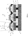
- FIG. 2 shows an LED device 10 according an illustrative example not forming part of the invention as claimed, which builds on the LED device 10 shown in FIG. 1 .
- the LED device 10 is show in a side-view/cross section (left side) and in a top view (right side). Same elements in FIG. 1 and FIG. 2 share the same reference signs and function likewise.
- the LED device 10 of FIG. 2 comprises the LED array 11, the top and bottom contacts 13 and 14, respectively, and the conductive structure 15.
- FIG. 2 shows particularly an LED device 10, in which a damascene process was used to fabricate the conductive structure 15.
- the damascene process can be similar to one used in M10-M14 in advanced logic processes.
- the conductive structure 15 may comprise a metallic core, particularly a Cu core, if a Cu-damascene process is used, and may be embedded in a dielectric material 24, which is here selected to be SiO2.
- the dielectric material 24 is particularly transparent for the light of the LED array 11.
- the conductive structure 15 may further comprise a light absorbing layer 26, i.e. an anti-reflective layer, configured to absorb light emitted by the plurality of LEDs 12 and impinging on the surface of the conductive structure 15, i.e. absorb the first part of the light.
- a light absorbing layer 26 i.e. an anti-reflective layer, configured to absorb light emitted by the plurality of LEDs 12 and impinging on the surface of the conductive structure 15, i.e. absorb the first part of the light.
- An example for such an anti-reflective layer is a (black) carbon layer, particularly a PECVD C layer (with a thickness of e.g. 5-50nm), or a layer of a high refractive index material to trap light (e.g. ALD Al 2 O 3 ).
- the absorbing layer 26 may be provided, e.g.
- an absorptive surface or absorptive surface regions of the conductive structure 15 are formed.
- the conductive structure 15 may be positioned on a transparent common top contact 13 (shown to be ITO, but it can also be highly doped n-GaN or p-GaN). As shown in the top view of FIG. 2 , the conductive structure 15 may be shaped gridlike - e.g. as a grid forming a honeycomb pattern - and may follow the contours of the plurality of LEDs 12 arranged beneath it (when viewed in the top view). The conductive structure 15 may define also a plurality of transparent openings 21 located at a certain distance above the LEDs 12, each opening 21 being related to one of the plurality of LEDs 12.
- the conductive structure 15 may particularly be formed by a plurality of vertical posts 20, the vertical posts 20 being positioned above the spaces between the plurality of LEDs 12, in order to separate each LED 12 from its adjacent LEDs 12 in the LED array 11.
- the transparent openings 21 may be defined, one opening 21 related to and arranged above each LED 12
- One or more vertical post 21 may together be arranged around one of the LEDs 12 in a top view, that is, may follow the outer contours of an LED 12.
- the conductive structure 15 helps guaranteeing a uniform current distribution and also avoiding optical cross talk between different LED pixels, i.e. between adjacent LEDs 12.
- the vertical posts 20 may prevent light emitted by one LED 12 from reaching a neighboring LED 12 and/or from passing through the opening 21 related to a neighboring LED 12.
- FIG. 2 shows also some exemplary dimensions of the LED device 10.
- a distance between vertical posts 20 of the conductive structure 15 in a cross-section may be between 2-4 ⁇ m, particularly about 3 ⁇ m (see left side). This diameter may be equal to the LED pixel pitch.
- a size (width or diameter d) of an opening 21 in the conductive structure 15 may be below 2 ⁇ m, or below 1 ⁇ m, or even below 500nm.
- a height of the conductive structure 15 may be between 1-3 ⁇ m, particularly about 2 ⁇ m. This height may be in the order of the LED pixel pitch.
- the conductive structure 15 may have a height between 0.5-0.8 times the LED pixel pitch of the LED array 11.
- a vertical thickness of the LEDs 12 may be between 100-300nm, particularly may be about 200nm as shown in FIG. 2 .
- the LEDs 12 may be GaN-based LEDs.
- a vertical thickness of the top contact 13 may be between 50-150 nm, particularly about 100nm as shown in FIG. 2 .
- each bottom contact 14 may include a contact layer 25, e.g. a highly-doped p-type semiconductor material, which is applied to the bottom surface of one of the LEDs 12.
- the contact layer 25 may also function as mirror (as indicated in FIG. 2 ), in order to support directing the light of the LED 12 along the main emission axis 18.
- each bottom contact 14 may include an electrical connection element, e.g. a via 28, electrically connected to a CMOS IC 22 arranged below the LED array 11. That is, the LED device 10 may comprise the CMOS IC 22, which is connected through the bottom contacts 14 to the LEDs 12, and is configured to drive and/or readout the LED array 11.
- each LED 12 can be driven/read out individually by means of one of the bottom contacts 14 and one or more top contacts 13.
- the at least one top contact 13 may be connected by at least one electrical connection element, particularly a via, to the CMOS IC 22.
- the at least one electrical connection element is passed by or around the LED array 11, i.e. the electrical connection element does not go through the LED array 11.
- the electrical connection element would be arranged outside/next to the LED array 11.
- FIG. 3 shows an LED device 10 according to an illustrative example not forming part of the invention as claimed, which builds on the LED device 10 shown in FIG. 1 and particularly FIG. 2 . Same elements in FIG. 3 and in FIG. 1 or FIG. 2 share the same reference signs and function likewise. Also the LED device 10 of FIG. 2 comprises the LED array 11, the top and bottom contacts 13 and 14, and the conductive structure 15.
- the conductive structure 15 is combined with a plurality of lenses 30, particularly with micro-lenses, e.g. polymer reflow lenses.
- Each of the lenses 30 is arranged above the conductive structure 15, particularly above an opening 21 of the conductive structure 15.
- Each lens 30 may cover one of the opening 21.
- Each of the lenses 30 is further configured to focus the light that is emitted by one of the LEDs 12 and is passed by the conductive structure 15, in this case through the associated opening 21.
- the lenses 30 focus the light again to a narrower beam, i.e. the focused light may have an emission angle 31 that is smaller than the emission angle 16 of the passed light.
- the emission angle 31 of the focused light may, for instance, be an angle below 60°, particularly an angle between 40-50°, i.e. it may be the same as the emission angle 16 of the passed light for the LED device 10 of FIG. 1 or FIG. 2 .
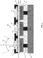
- FIG. 4 shows an LED device 10 according to an embodiment of the invention, which builds on the LED device shown in FIG. 1 and particularly FIG. 2 .
- the LED device 10 of FIG. 4 is primarily an alternative to the LED device 10 shown in FIG. 3 , but the two embodiments can also be combined. Same elements in FIG. 4 and in FIG. 1 or FIG. 2 share the same reference signs and function likewise.
- the LED device 10 of FIG. 2 comprises the LED array 11, the top and bottom contacts 13 and 14, and the conductive structure 15.
- a plurality of lenses 40 are arranged between the LED array 11 and the conductive structure 15.
- Each of the lenses 40 is e.g. configured to focus at least some of the light emitted by one of the plurality of LEDs 12, which would be absorbed by the conductive structure 15 without the lens 40 being present.
- the focused light may be passed by the conductive structure 15.
- the plurality of lenses 40 may be refractive lenses or gratings.
- the lenses 40 are arranged between the LED array 11 and the conductive structure 15 and/or within the conductive structure 15.
- the lenses 40 may be combined with the lenses 30 shown in FIG. 3 .
- An advantage over the LED device 10 shown in FIG. 2 is that the optical efficiency improves, since the intensity of the passed light is increased.
- light that is emitted by each LED 12 and impinges on the conductive structure 15 - and is thus not transmitted through the conductive structure 15 - is simply filtered out (i.e. absorbed).
- some of that light may be focused and transmitted through the conductive structure 15.
- the intensity of the passed light with the emission angle 16 can be increased.
- an emission angle 41 of the light focused by the lenses 40 may be smaller than the emission angle 16 of the passed light.
- a dielectric 24 surrounding the conductive structure 15, i.e. a dielectric 24 that may result from using a damascene process may be one of e.g. SiO 2 , SiN, aSi or TiO 2 .
- the high refractive index layer 26 provided on the core 27 of the conductive structure 15 - as an alternative to a carbon layer - in order to make the conductive structure 15 absorptive for the LED light may e.g. be Al 2 O 3 or TiO.
- the high refractive index layer 26 may, for instance, be deposited by Atomic Layer Deposition (ALD), in order to create a reflector configured to trap light in between the conductive core 27 of the conductive structure 15, e.g. Cu core, and the dielectric interface.
- ALD Atomic Layer Deposition
- FIG. 5 shows initial steps of a method 50 for fabricating an LED device 10 according to the illustrative examples and according to the embodiment of the invention.
- the method 50 includes a step 51 of processing a LED array 11 including a plurality of LEDs 12. Further, it includes a step 52 of processing at least one top contact 13 and at least one bottom contact 14 electrically connected to the LED array 11. Further, it includes a step 53 of processing, particularly by using a damascene process, e.g. using a dual-damascene Cu process, a conductive structure 15 arranged above the LED array 11 and the top contact 13, respectively, and electrically connected to the top contact 13.
- a damascene process e.g. using a dual-damascene Cu process
- the conductive structure 15 is processed such that it is, regarding each LED 12, configured to absorb a first part of the light emitted by the LED 12, and to pass a second part of the light. Thereby, the conductive structure 15 is processed such that, in operation of the fabricated LED device 100, an emission angle 16 of the passed light is smaller than an emission angle 17 of the light emitted by the LED 12.
Description
- The present invention relates to the technical field of Light Emitting Diode (LED) devices, particularly of micro-LED (µLED) devices. The invention presents an LED device with an LED array, particularly with a µLED array having a LED pixel pitch in the µm range. An emission angle of the light provided by the LED device is reduced compared to an emission angle of the light output from the LED array. Thus, the LED device of the invention is well applicable to µLED displays as, for instance, used in augmented reality (AR) glasses.
- The emission angle (also referred to as the "beam angle" or "APEX angle") of light emitted by a light source - e.g. a LED device or array - is the opening angle of the emitted "light beam" or "light cone". The emission angle is particularly defined as the angle between the two emission directions, for which the luminous intensity is reduced to 50% of the luminous intensity along a main emission axis/direction of the light source. For rotational symmetric beams, the emission angle is thus twice a certain angle with respect to the main emission axis (also referred to as the "optical axis"), at which the luminous intensity is reduced to 50% of the luminous intensity along the main emission axis. The main emission axis is the direction, into which the light source emits the highest relative luminous intensity.
- The emission angle of light emitted by a conventional µLED array in a LED device is typically between 110-160°. Outside of this rather wide emission angle, the light intensity is significantly reduced or lost, e.g. due to internal reflections.
- However, in order to use a LED device with a µLED array in e.g. a µLED display, the emission angle of the light it emits should be much narrower than the above-mentioned emission angle of the conventional µLED array. In particular, the light emission angle of such a LED device should ideally be around 50° or less, in order to allow collimation of the emitted light into, for example, a waveguide.
- To reduce the emission angle of a conventional µLED array towards this narrow target specification, in principle a diaphragm or optical lens could be used to collimate the light. However, due to the strict size limitations in a LED device with a µLED array, for instance, for the LED pixel pitch being in the µm range, and in view of the ongoing efforts to scale down further this pixel pitch, the design of a diaphragm or lens for such a LED device is very challenging. As of now, no satisfying solution for a LED device with a LED array is available.
- Another challenge for a LED device including a conventional µLED array is that the smaller the LED pixel pitch is or becomes, the more difficult it is to provide for an efficient current and heat distribution in the device.
-
US 2015/362165 A1 discloses a light engine array comprising multiple light engines, and a dam array comprising multiple dams located on a surface of the light engines. -
US 2017/294424 A1 discloses a display apparatus comprising LEDs, and a method of manufacturing the same. -
EP 3 410 479 A1 discloses a display device comprising light-emitting elements on a substrate. - In view of the above-mentioned challenges, embodiments of the present invention aim to improve conventional LED devices with LED arrays, particularly with µLED arrays, and their fabrication process. An objective thereby is to provide a LED device, which emits light with a narrow emission angle. The emission angle should be narrow enough to allow for an efficient collimation and coupling of the light into, for instance, a waveguide. The emission angle of the LED device should especially be well below the emission angle of a conventional µLED array.
- Moreover, the above objective should be achieved even for very small LED pixel pitches, i.e. in the low µm range. In addition, an efficient heat and current distribution should also be provided in the LED device, particularly in its LED array. Another goal is to fabricate the LED device very compactly, and with an efficient fabrication process that allows reaching high yields.
- The objective of the present invention is achieved by the embodiments of the invention provided in the enclosed independent claims. Advantageous implementations of these embodiments are defined in the dependent claims.
- A first aspect of the invention relates to a LED device, comprising: a LED array including a plurality of LEDs, at least one top contact and bottom contact electrically connected to the LED array, and a conductive structure arranged above the LED array and the top contact, respectively, and electrically connected to the top contact, wherein the conductive structure is, regarding each LED, configured to absorb a first part of the light emitted by the LED, and to pass a second part of the light emitted by the LED, wherein an emission angle of the passed light is smaller than an emission angle of the light emitted by the LED, and wherein the LED device is characterized by further comprising: a plurality of lenses arranged between the LED array and the conductive structure, wherein each lens is configured to focus at least some of the light emitted by one of the plurality of LEDs, so that the focused light is passed by the conductive structure.
- The conductive structure is configured like this with respect to each single LED in the LED array. An emission angle of the passed light being smaller than an emission angle of the light emitted by the LED means the same as that the conductive structure is configured to pass the light emitted by the LED as a collimate beam.
- In particular, the conductive structure is configured to absorb the first part of the LED light by having an absorptive surface or at least an absorptive surface region arranged in the light path. The conductive structure is further configured to pass the second part of the LED light by having an opening arranged above the LED and transparent at least to the light emitted by the LED. The conductive structure is particularly arranged such with respect to the LED beneath it, that the beam angle of the light passing through the opening is narrowed compared to the beam angle of the LED light. That is, the conductive structure serves as a diaphragm. This may be achieved by properly designing the width and height of the conductive structure, and the width or diameter of the openings in the conductive structure.
- Each LED of the LED array is configured to emit light along a certain main emission axis and with a certain emission angle (which is symmetrically around the main emission axis). That is, each LED is configured to output a light beam or light cone with the emission angle being its (APEX) opening angle. For instance, the emission angle of each LED, and thus also of the LED array as a whole, may be between 110-160° (i.e. before the conductive structure and without any optical elements acting on the light).
- The conductive structure absorbs LED light that impinges on it (first part), while it lets the remaining LED light (second part) pass through. Because the LED light has a smaller beam angle after passing the conductive structure than before passing it, an APEX reduction of the emitted light is achieved in the LED device. Notably, the emission angle of the passed light may be the emission angle of the light output by the LED device as a whole, if the passed light is not affected anymore by any further optical element of the LED device.
- The conductive structure advantageously has a twofold purpose in the LED device. On the one hand, it serves as the diaphragm arranged above the LED array, as described above. On the other hand, since it is electrically connected to the at least one top contact, it can be used to provide a current or voltage to the LED array. In particular, it thus enables an efficient current distribution. Furthermore, it also provides for an efficient heat distribution during operation of the LED device.
- As a consequence, the LED device of the first aspect is particularly suited for being used in a top emission µLED display.
- Further, each of the lenses focuses at least some light of the LED, which the conductive structure would otherwise be arranged and configured to absorb, i.e. without the lens being present. While the emission angle of the passed light, i.e. after the conductive structure, may still be defined primarily by the dimensions and the arrangement of the conductive structure with respect to the LED - and not by the lens arranged regarding this LED between the LED array and the conductive structure - the total intensity of the passed light may be increased. The lenses may be microlenses, reflow lenses, and/or refractive lenses. The lenses are arranged below the conductive structure, but above the LED array and top contact, respectively. However, the lenses may also be arranged above a lower end of the conductive structure but below an upper end of the conductive structure, i.e. within the height of the conductive structure.
- The lenses may, according to an example not forming part of the claimed invention, be diffractive lenses, in which case the lenses do not focus but widen the light coming from the LEDs. In this case, the conductive structure may be configured to reflect at least some of the widened light such that it passes the conductive structure. For this, the conductive structure may be provided with a reflective surface at least in determined surface regions.
- Notably, as already described generally above, the main emission axis (optical axis) of each LED of the LED device is the axis, into which that LED emits the highest relative luminous intensity. This optical axis maybe perpendicular to the LED surface, the LED layers and/or particularly to an active area, e.g. a quantum well layer, of the LED. The LED, however, also emits light into directions deviating from the main emission axis, however, at lower relative luminous intensity. At two certain angles from the main emission axis (in opposite angular directions from the main emission axis), the luminous intensity of the emitted light drops to 50%. The two certain angles determine the emission angle (beam angle) of the light emitted by the LED, namely the emission angle of the light emitted by the LED is the sum of these certain angles (and is twice the same certain angle for a rotational symmetric beam.
- The emission angle (beam angle) of the passed light may be determined likewise. That is, the light of a certain LED passes the conductive structure with a certain main emission axis, in which the passed light has the highest relative luminous intensity. This main emission axis of the passed light typically, but not necessarily, coincides with the main emission axis of the LED. The emission angle of the passed light is defined by the sum of the angles from the main emission axis of the passed light to opposite sides thereof, at which the luminous intensity of the passed light drops to 50%. If the passed light is rotation symmetric the emission angle is twice the same angle from the main emission axis to each side, at which the passed light drops to 50%.
- The at least one top contact electrically contacts the LEDs of the LED array from above. For instance, each LED may be contacted by a single top contact provided on its top surface. Preferably, however, a common top contact covers the top surface of multiple LEDs or all LEDs. The at least one bottom contact contacts each LED from below. For instance, each LED may be contacted by one single bottom contact from below.
- Notably, the conductive structure and the at least one top contact are separate structures. However, together they may be considered to form a top contact structure in the LED device for contacting the LED array.
- The terms "above" and "below" relate to the orientation of the LEDs and particularly the light emission axis/direction of the LED array. "Above" or "top" is the side where the LED array emits light. "Below" or "bottom" is the opposite side. Any element referred to as being "below" the LEDs or the LED array does thus not interfere with the emitting of the LED light.
- In an implementation of the LED device, the emission angle of the passed light is an angle of 60° or less, particularly is an angle of 40-50°.
- Thus, the emission angle of the LED device becomes narrow enough - even without any further optical elements - to be well coupled into a waveguide or the like. Accordingly, the LED device is well suited for application in a µLED display.
- In an implementation, the LED device further comprises a plurality of lenses arranged above the conductive structure, wherein each lens is configured to focus the light that is emitted by one of the plurality of LEDs and is passed by the conductive structure.
- In this implementation, the emission angle of the passed light, i.e. after the conductive structure, may be larger than described above. For instance, the emission angle of the passed light may be an angle above 60°, or even an angle above 100°, since the lens provided for each LED above the conductive structure further narrows the beam of the passed light. That is, an emission angle of the focused light is smaller than the emission angle of the passed light. The emission angle of the focused light may in this case be the emission angle of the light output by the LED device as a whole, if the light coming from the lenses is not influenced anymore by any further optical element of the LED device. The lenses may be microlenses, reflow lenses, and/or refractive lenses.
- If the emission angle of the passed light is an angle between 60-100°, as exemplarily described above, the emission angle of the focused light may an angle below 60°, e.g. an angle between 40-50°. In this way, the dimensions of the conductive structure, which lead to the emission angle reduction regarding each of the LEDs, can be designed larger, thus processing of it becomes simpler.
- If the emission angle of the passed light is already an angle below 60°, as also described exemplarily above, the emission angle of the focused light may be an angle below 40°, e.g. an angle between 25-40°. In this way, an even narrower emission angle of the LED device as a whole becomes possible.
- In an implementation of the LED device, the conductive structure comprises a light-absorbing layer to absorb light emitted by the plurality of LEDs, particularly a carbon layer or a layer of a high refractive index material.
- The light-absorbing layer may be disposed onto the outer surface of a conductive core of the conductive structure, at least onto determined surface regions arranged in the path of LED light that is to be removed. However, also the complete surface of the core of the conductive structure may be coated with such an absorbing layer. In this way, the conductive structure may be configured to absorb the first part of the light emitted by each LED, in order to reduce the emission angle. For instance, when considering a central point of light emission in the LED active area, i.e. the point in the LED active area through which the optical axis of the LED extends, light emitted from this point at angles below a determined angle may pass the conductive structure, while light emitted from this point above a determined angle may be absorbed by the conductive structure. For the light emitted from this point, the emission angle is thus narrowed.
- A carbon layer is simply very black and is thus absorptive. A high refractive index material (e.g. ALD Al2O3) will let light coming from the LED pass (due to the refractive index change), but the light will reflect at the core of the conductive structure and cannot anymore pass the high refractive index material in the opposite direction. Thus, the light enters the layer of the high refractive index material, where it is trapped.
- In an implementation, the LED device further comprises a transparent top contact connected to several or each of the plurality of LEDs and arranged between the LED array and the conductive structure.
- That is, the transparent top contact is a common top contact, common to at least some of the LEDs. The top contact is particularly transparent to the LED light. The common top contact simplifies the processing of the LED device, and allows designing a smaller LED array with an optimized overall area occupied by LED surface (aperture).
- In an implementation of the LED device the conductive structure is connected to determined regions of a top surface of the top contact, the determined regions being positioned above the spaces between adjacent LEDs.
- In particular, the determined regions may be only positioned above the spaces between the LEDs, not above the LEDs themselves. Accordingly, the determined regions may be aligned with the spaces when the LED device is viewed in a top view, i.e. from above. In other words, the conductive structure as a whole is put on the top contact such that it follows the spaces between the multiple LEDs beneath the top contact. In this way, the conductive structure is able to contact the top contact, to serve as a diaphragm for each of the LEDs, and to separate the light coming from different LEDs.
- In an implementation of the LED device, the conductive structure comprises a plurality of transparent openings, each transparent opening being related to one of the plurality of LEDs.
- In particular, each transparent opening may be arranged above the LED it is related to. "Transparent" opening means that the opening is configured to pass at least the light of interest emitted by the LED it is related to. The transparent openings can be realized with a transparent material being embedded into cavities of the conductive structure and located above the LEDs. The transparent openings may filter electromagnetic radiation other than the light of interest of the LEDs.
- In an implementation of the LED device, the conductive structure comprises a plurality of vertical posts, the vertical posts being positioned above the spaces between the plurality of LEDs and configured to separate adjacent LEDs from each other.
- In particular, the vertical posts are aligned with the contours of the LEDs in a top view of the LED device. Each LED may be surrounded by one or more vertical posts, in the top view. The vertical posts may have an absorptive surface facing the LEDs, or may at least absorptive regions on that surface. The vertical posts separate adjacent LEDs from each other with respect to the light emitted by each LED being separated.
- In an implementation of the LED device, an upper surface of the conductive structure defines the transparent openings and is located at a determined distance above the LED array.
- The determined distance and a size (e.g. a width or diameter) of each an opening determines with respect to an LED, how strong the reduction of the emission angle of the passed light is with respect to the light emitted by this LED.
- In an implementation of the LED device, the LED array has a LED pixel pitch between 1-10µm, in particular equal to or below 3µm, and/or a height of the conductive structure is between 0.1-1 times, in particular between 0.5-0.8 times, a LED pixel pitch of the LED array.
- Thus, the LED array is particularly a µLED array. The LEDs in this array can be placed closely together, thus allowing a very compact LED device but with maximized LED apertures. The height of the conductive structure is in the range of the LED pixel pitch, and thus works well as the diaphragm.
- In an implementation of the LED device, the conductive structure comprises a metallic core, particularly a copper core, and is embedded in a dielectric material.
- Accordingly, the conductive structure may be a damascene-processed structure, i.e. may be produced by using a damascene process. In particular, this may be a damascene copper (Cu) process and/or a dual-damascene process. Alternatively it can be a tungsten (W) damascene process or ruthenium (Ru) damascene process as well. The dielectric is preferably transparent for the LED light. By using a damascene process, the conductive structure can be made in one process step, and can be made such that it serves as a highly conductive metallization grid for efficient current and heat distribution in the LED device, and serves as the diaphragm reducing the emission angle of the LED light.
- In an implementation, the LED device further comprises a plurality of bottom contacts, wherein each bottom contact is electrically connected to one of the plurality of LEDs, and a CMOS IC connected through the bottom contacts to the LEDs and configured to drive the LED array.
- The CMOS IC may also be configured to readout the LED array. The CMOS IC may include an active matrix of logical elements, one associated with each LED of the LED array. One bottom contact per LED is provided below the LED array. The CMOS IC may be provided directly beneath the bottom contacts, i.e. close to the LED array.
- In an implementation of the LED device, the LED device is an integrated LED chip or wafer, wherein particularly the LED array, the at least one top and bottom contact and the conductive structure are integrated.
- In particular, even a monolithic integration of the LED device, particularly the mentioned elements, is possible. The LED device can thus be fabricated in a very compact manner and with an efficient process.
- A second aspect of the invention relates to a method for fabricating a LED device, the method comprising: processing a LED array including a plurality of LEDs, processing at least one top contact and bottom contact electrically connected to the LED array, and processing, particularly with a damascene process, a conductive structure arranged above the LED array and the top contact, respectively, and electrically connected to the top contact, wherein the conductive structure is, regarding each LED, configured to absorb a first part of the light emitted by the LED, and to pass a second part of the light emitted by the LED, wherein an emission angle of the passed light is smaller than an emission angle of the light emitted by the LED, and wherein the method is characterized by further comprising: processing a plurality of lenses between the LED array and the conductive structure, wherein each lens is configured to focus at least some of the light emitted by one of the plurality of LEDs, so that the focused light is passed by the conductive structure.
- The conductive structure can either be a single-layer structure or a dual-layer structure (when fabricated in a dual-damascene process), wherein at least one of these layers is configured to absorb the first part of the light, for instance, by being provided with an anti-reflective coating.
- The method of the second aspect may be developed in implementation forms according to the implementation forms described for the LED device of the first aspect.
- The above described aspects and implementations are explained in the following description of embodiments with respect to the enclosed drawings:
-
FIG. 1 shows a LED device according to an illustrative example not forming part of the invention as claimed. In particular, a LED device with a conductive structure arranged above an LED array. -
FIG. 2 shows a LED device according to an illustrative example not forming part of the invention as claimed. In particular, an LED device in which the conductive structure is fabricated by a damascene process. -
FIG. 3 shows a LED device according to an illustrative example not forming part of the invention as claimed. In particular, a LED device, which includes the conductive structure in combination with a plurality of lenses disposed above the conductive structure. -
FIG. 4 shows a LED device according to an embodiment of the invention. In particular, a LED device, which includes the conductive structure in combination with a plurality of lenses disposed between the conductive structure and the LED array. -
FIG. 5 shows initial steps of a method according to an embodiment of the invention for producing an LED device. -
FIG. 1 shows aLED device 10 according to an illustrative example not forming part of the invention as claimed. - The
LED device 10 may particularly be a µLED device, which is suitable for being used in a µLED display. TheLED device 10 may be an integrated chip or wafer, e.g. monolithically integrated. - The LED device comprises a
LED array 11, particularly a µLED array, which includes a plurality ofLEDs 12. TheLEDs 12 of theLED array 11 may, for example, be arranged in rows and/or columns, or in any other two-dimensional pattern. An LED pixel pitch, i.e. a center-to-center distance between adjacent LEDs 12 (i.e. the sum of LED width/diameter and the space between adjacent LEDs 12) may be in the µm range, particularly may be equal to or below 3µm. EachLED 12 of theLED array 11 is configured to emit light, wherein anemission angle 17 of the emitted LED light may be between 110°-160°. That means, eachLED 12 can emit light with acertain beam angle 17. Theemission angle 17 of eachLED 12 is preferably similar or equal. Due to the close arrangement of theLEDs 12, an emission angle of the light emitted by theLED array 11 as a whole is the same as theemission angle 17. - Further, the
LED device 10 includes at least onetop contact 13 electrically connected to theLED array 11 from above, and at least onebottom contact 14 electrically connected to the LED array from below. "Above" and "below" are defined along themain emission axis 18 of each LED 12 (parallel to the vertical direction inFIG. 1 ), wherein it is assumed that the main emission axes 18 of theLEDs 12 are parallel. EachLED 12 is contacted by at least onetop contact 13 andbottom contact 14, and when a sufficient voltage is applied between these twocontacts LED 12 emits the light. EachLED 12 may have its owntop contact 13 and/or itsown bottom contact 14, but also common contacts can be applied toseveral LEDs 12 or even all of theLEDs 12 in theLED array 11. The at least onetop contact 13 may particularly made of a transparent conductive material, for instance: Indium Tin Oxide (ITO), highly-doped n-GaN, or highly-doped p-GaN. - Notably, there is no vertical interconnect access (via) or any other electrical connection element through the
LED array 11 and between theLEDs 12. In this way, the LED pixel pitch equal to or smaller than 3µm can be achieved, while the optical apertures of theLEDs 12 can be maximized, i.e. the LED surfaces occupy as much area of theLED array 11 as possible. - The
LED device 10 further comprises aconductive structure 15, which is arranged above theLED array 11 and above the at least onetop contact 13, respectively. Theconductive structure 15 is electrically connected to thetop contact 13. Thus, it can be used to provide current to theLED array 11, and also serves as heat distributor during operation of the LEDs 112. In particular, theconductive structure 15 is provided on thetop contact 13, at least on dedicated regions of its top surface, particularly regions of the top surface of thetop contact 13, which are positioned above the spaces betweenadjacent LEDs 12 in theLED array 11 below thetop contact 13. - The
conductive structure 15 is further configured to act as a diaphragm for theLED array 11, particularly for eachLED 12, in order to narrow the emission angle regarding eachLED 12 and thus of theLED array 11 as a whole. To this end, theconductive structure 15 is dimensioned, arranged and configured, regarding each of theLEDs 12, such that - in operation of the LED device 10 - it absorbs a first part of the light emitted by theLED 12, and passes a second part of light emitted by theLED 12. The first part that is absorbed is light emitted by theLED 12 hitting an absorptive surface or surface region of theconductive structure 15, and the second part that is passed is light emitted by theLED 12 that does not hit theconductive structure 15, because it goes through a dedicated opening in theconductive structure 15. Thereby, anemission angle 16 of the passed light, i.e. after theconductive structure 15, is smaller than theemission angle 17 of the light emitted by theLED 12, i.e. before the conductive structure. Accordingly an APEX reduction perLED 12 is achieved. -
FIG. 1 illustrates schematically, how theconductive structure 15 is configured to output/pass light, regarding each of theLEDs 12, with the narrowedemission angle 16. TheLED 12 emits light primarily along themain emission axis 18, but with theemission angle 17, which symmetrically centers themain emission axis 18. TheLED 12, particularly an active area thereof, like a quantum well, has a certain finite width/diameter as seen inFIG. 1 . The width of theLED 12 may be in the order of the dimensions of theconductive structure 15. For example, a height of theconductive structure 15 may be between 0.5-0.8 times the LED pixel pitch of theLED array 11, and may thereby be equal to the width/diameter of theLED 12. Each point of the active area of theLED 12 emits light, due to carrier recombination, and each emission is assumed to have thesame emission angle 17. - The conductive structure is 15 now placed such with the respect to each
LED 12 that it forms an opening over theLED 12. For instance, theoptical axis 18 of theLED 12 may be centered in the corresponding opening of theconductive structure 15. Accordingly, light emitted along theoptical axis 18 may pass theconductive structure 15. However, also light not emitted along theoptical axis 18 may be able to pass theconductive structure 15, as indicated by the dotted lines originating from the two opposite edges of theLEDs 12. Theemission angle 16 of the light passed by theconductive structure 15 is defined by basic geometrical considerations. - The opening related to each
LED 12 should to have a certain diameter/width, and should be arranged at a certain distance above theLED 12. These parameters depend on theemission angle 17 of theLED 12, the width of theLED 12, the desiredemission angle 16 of the passed light, and on each other. The latter means that a wider opening of theconductive structure 15 may be used for a higherconductive structure 15, i.e. for a larger distance between the opening and theLED 12. - In an example, the
emission angle 17 of theLED 12 is between 110-160°, while theemission angle 16 of the passed light is below 60°, particularly is between 40-50°. However, the value of theemission angle 16 of the passed light can be adjusted by adjusting the dimensions (e.g. height, opening width/diameter, LED-opening-distance) of theconductive structure 15 and/or its arrangement with respect to theLED array 11. -
FIG. 2 shows anLED device 10 according an illustrative example not forming part of the invention as claimed, which builds on theLED device 10 shown inFIG. 1 . Particularly, theLED device 10 is show in a side-view/cross section (left side) and in a top view (right side). Same elements inFIG. 1 andFIG. 2 share the same reference signs and function likewise. Also theLED device 10 ofFIG. 2 comprises theLED array 11, the top andbottom contacts conductive structure 15.FIG. 2 shows particularly anLED device 10, in which a damascene process was used to fabricate theconductive structure 15. The damascene process can be similar to one used in M10-M14 in advanced logic processes. Accordingly, theconductive structure 15 may comprise a metallic core, particularly a Cu core, if a Cu-damascene process is used, and may be embedded in adielectric material 24, which is here selected to be SiO2. Thedielectric material 24 is particularly transparent for the light of theLED array 11. The use of the damascene process allows creating a high aspect ratioconductive structure 15, which is beneficial for sheet resistance, but at the same time for the function of a diaphragm. - As shown in the enlarged section of
FIG. 2 , theconductive structure 15 may further comprise alight absorbing layer 26, i.e. an anti-reflective layer, configured to absorb light emitted by the plurality ofLEDs 12 and impinging on the surface of theconductive structure 15, i.e. absorb the first part of the light. An example for such an anti-reflective layer is a (black) carbon layer, particularly a PECVD C layer (with a thickness of e.g. 5-50nm), or a layer of a high refractive index material to trap light (e.g. ALD Al2O3). The absorbinglayer 26 may be provided, e.g. grown, sputtered, or dispensed, or the like, onto an outer surface of aconductive core 27 of theconductive structure 15, or at least onto regions of that core surface. Thus, an absorptive surface or absorptive surface regions of theconductive structure 15 are formed. - The
conductive structure 15 may be positioned on a transparent common top contact 13 (shown to be ITO, but it can also be highly doped n-GaN or p-GaN). As shown in the top view ofFIG. 2 , theconductive structure 15 may be shaped gridlike - e.g. as a grid forming a honeycomb pattern - and may follow the contours of the plurality ofLEDs 12 arranged beneath it (when viewed in the top view). Theconductive structure 15 may define also a plurality oftransparent openings 21 located at a certain distance above theLEDs 12, each opening 21 being related to one of the plurality ofLEDs 12. Theconductive structure 15 may particularly be formed by a plurality ofvertical posts 20, thevertical posts 20 being positioned above the spaces between the plurality ofLEDs 12, in order to separate eachLED 12 from itsadjacent LEDs 12 in theLED array 11. Above thevertical posts 20, thetransparent openings 21 may be defined, oneopening 21 related to and arranged above eachLED 12 One or morevertical post 21 may together be arranged around one of theLEDs 12 in a top view, that is, may follow the outer contours of anLED 12. Thus, theconductive structure 15 helps guaranteeing a uniform current distribution and also avoiding optical cross talk between different LED pixels, i.e. betweenadjacent LEDs 12. For instance, thevertical posts 20 may prevent light emitted by oneLED 12 from reaching a neighboringLED 12 and/or from passing through theopening 21 related to a neighboringLED 12. -
FIG. 2 shows also some exemplary dimensions of theLED device 10. For instance, a distance betweenvertical posts 20 of theconductive structure 15 in a cross-section may be between 2-4µm, particularly about 3µm (see left side). This diameter may be equal to the LED pixel pitch. A size (width or diameter d) of anopening 21 in theconductive structure 15 may be below 2µm, or below 1µm, or even below 500nm. A height of theconductive structure 15 may be between 1-3µm, particularly about 2µm. This height may be in the order of the LED pixel pitch. Generally speaking, theconductive structure 15 may have a height between 0.5-0.8 times the LED pixel pitch of theLED array 11. Further, a vertical thickness of theLEDs 12 may be between 100-300nm, particularly may be about 200nm as shown inFIG. 2 . TheLEDs 12 may be GaN-based LEDs. A vertical thickness of thetop contact 13 may be between 50-150 nm, particularly about 100nm as shown inFIG. 2 . -
FIG. 2 also shows that eachbottom contact 14 may include acontact layer 25, e.g. a highly-doped p-type semiconductor material, which is applied to the bottom surface of one of theLEDs 12. Thecontact layer 25 may also function as mirror (as indicated inFIG. 2 ), in order to support directing the light of theLED 12 along themain emission axis 18. Further, eachbottom contact 14 may include an electrical connection element, e.g. a via 28, electrically connected to aCMOS IC 22 arranged below theLED array 11. That is, theLED device 10 may comprise theCMOS IC 22, which is connected through thebottom contacts 14 to theLEDs 12, and is configured to drive and/or readout theLED array 11. Thereby, eachLED 12 can be driven/read out individually by means of one of thebottom contacts 14 and one or moretop contacts 13. To this end, the at least onetop contact 13 may be connected by at least one electrical connection element, particularly a via, to theCMOS IC 22. Thereby, the at least one electrical connection element is passed by or around theLED array 11, i.e. the electrical connection element does not go through theLED array 11. In other words, in a top view of theLED array 11, the electrical connection element would be arranged outside/next to theLED array 11. -
FIG. 3 shows anLED device 10 according to an illustrative example not forming part of the invention as claimed, which builds on theLED device 10 shown inFIG. 1 and particularlyFIG. 2 . Same elements inFIG. 3 and inFIG. 1 orFIG. 2 share the same reference signs and function likewise. Also theLED device 10 ofFIG. 2 comprises theLED array 11, the top andbottom contacts conductive structure 15. - In the
LED device 10 shown inFIG. 3 , theconductive structure 15 is combined with a plurality oflenses 30, particularly with micro-lenses, e.g. polymer reflow lenses. Each of thelenses 30 is arranged above theconductive structure 15, particularly above anopening 21 of theconductive structure 15. Eachlens 30 may cover one of theopening 21. Each of thelenses 30 is further configured to focus the light that is emitted by one of theLEDs 12 and is passed by theconductive structure 15, in this case through the associatedopening 21. An advantage over theLED device 10 shown inFIG. 2 is that theconductive structure 15, which acts as the diaphragm, can be constructed less tightly, i.e. withwider openings 21, therefore resulting in awider emission angle 16 of the passed light compared to the one achieved inFIG. 1 or2 . However, thelenses 30 focus the light again to a narrower beam, i.e. the focused light may have anemission angle 31 that is smaller than theemission angle 16 of the passed light. Theemission angle 31 of the focused light may, for instance, be an angle below 60°, particularly an angle between 40-50°, i.e. it may be the same as theemission angle 16 of the passed light for theLED device 10 ofFIG. 1 orFIG. 2 . -
FIG. 4 shows anLED device 10 according to an embodiment of the invention, which builds on the LED device shown inFIG. 1 and particularlyFIG. 2 . TheLED device 10 ofFIG. 4 is primarily an alternative to theLED device 10 shown inFIG. 3 , but the two embodiments can also be combined. Same elements inFIG. 4 and inFIG. 1 orFIG. 2 share the same reference signs and function likewise. Also theLED device 10 ofFIG. 2 comprises theLED array 11, the top andbottom contacts conductive structure 15. - In the
LED device 10 ofFIG. 4 , a plurality oflenses 40 are arranged between theLED array 11 and theconductive structure 15. Each of thelenses 40 is e.g. configured to focus at least some of the light emitted by one of the plurality ofLEDs 12, which would be absorbed by theconductive structure 15 without thelens 40 being present. The focused light may be passed by theconductive structure 15. The plurality oflenses 40 may be refractive lenses or gratings. Thelenses 40 are arranged between theLED array 11 and theconductive structure 15 and/or within theconductive structure 15. Thelenses 40 may be combined with thelenses 30 shown inFIG. 3 . - An advantage over the
LED device 10 shown inFIG. 2 is that the optical efficiency improves, since the intensity of the passed light is increased. In theLED device 10 ofFIG. 2 , light that is emitted by eachLED 12 and impinges on the conductive structure 15 - and is thus not transmitted through the conductive structure 15 - is simply filtered out (i.e. absorbed). In theLED device 10 ofFIG. 4 , however, some of that light may be focused and transmitted through theconductive structure 15. Thus, in total more light may be passed by theconductive structure 15. That is, in theLED device 10 ofFIG. 4 , the intensity of the passed light with theemission angle 16 can be increased. For instance, anemission angle 41 of the light focused by thelenses 40 may be smaller than theemission angle 16 of the passed light. - In each of the above-described
LED devices 10 according to the illustrative examples and according to the embodiment of the invention (shown inFIG. 1-4 ) a dielectric 24 surrounding theconductive structure 15, i.e. a dielectric 24 that may result from using a damascene process, may be one of e.g. SiO2, SiN, aSi or TiO2. The highrefractive index layer 26 provided on thecore 27 of the conductive structure 15 - as an alternative to a carbon layer - in order to make theconductive structure 15 absorptive for the LED light, may e.g. be Al2O3 or TiO. The highrefractive index layer 26 may, for instance, be deposited by Atomic Layer Deposition (ALD), in order to create a reflector configured to trap light in between theconductive core 27 of theconductive structure 15, e.g. Cu core, and the dielectric interface. -
FIG. 5 shows initial steps of amethod 50 for fabricating anLED device 10 according to the illustrative examples and according to the embodiment of the invention. For instance, theLED devices 10 shown inFIG. 1-4 can be fabricated by using thismethod 50. Themethod 50 includes astep 51 of processing aLED array 11 including a plurality ofLEDs 12. Further, it includes astep 52 of processing at least onetop contact 13 and at least onebottom contact 14 electrically connected to theLED array 11. Further, it includes astep 53 of processing, particularly by using a damascene process, e.g. using a dual-damascene Cu process, aconductive structure 15 arranged above theLED array 11 and thetop contact 13, respectively, and electrically connected to thetop contact 13. Theconductive structure 15 is processed such that it is, regarding eachLED 12, configured to absorb a first part of the light emitted by theLED 12, and to pass a second part of the light. Thereby, theconductive structure 15 is processed such that, in operation of the fabricated LED device 100, anemission angle 16 of the passed light is smaller than anemission angle 17 of the light emitted by theLED 12.
Claims (14)
- Light Emitting Diode, LED, device (10), comprising:a LED array (11) including a plurality of LEDs (12),at least one top contact (13) and bottom contact (14) electrically connected to the LED array (11), anda conductive structure (15) arranged above the LED array (11) and the top contact (13), respectively, and electrically connected to the top contact (13),wherein the conductive structure (15) is, regarding each LED (12), configured to absorb a first part of the light emitted by the LED (12), and to pass a second part of the light emitted by the LED,wherein an emission angle (16) of the passed light is smaller than an emission angle (17) of the light emitted by the LED (12), andwherein the LED device (10) is characterized by further comprising:
a plurality of lenses (40) arranged between the LED array (11) and the conductive structure (15), wherein each lens (40) is configured to focus at least some of the light emitted by one of the plurality of LEDs (12), so that the focused light is passed by the conductive structure (15). - LED device (10) according to claim 1, wherein:
the emission angle (16) of the passed light is an angle of 60° or less, particularly is an angle of 40-50°. - LED device (10) according to claim 1 or 2, further comprising:
a plurality of lenses (30) arranged above the conductive structure (15), wherein each lens (30) is configured to focus the light that is emitted by one of the plurality of LEDs (12) and is passed by the conductive structure (15). - LED device (10) according to one of the claims 1 to 3, wherein:
the conductive structure (15) comprises a light-absorbing layer (27) to absorb light emitted by the plurality of LEDs (12), particularly a carbon layer or a layer of a high refractive index material. - LED device (10) according to one of the claims 1 to 4, comprising:
a transparent top contact (13) connected to several or each of the plurality of LEDs (12) and arranged between the LED array (11) and the conductive structure (15). - LED device (10) according to claim 5, wherein:
the conductive structure (15) is connected to determined regions of a top surface of the top contact (13), the determined regions being positioned above the spaces between adjacent LEDs (12). - LED device (10) according to one of the claims 1 to 6, wherein:
the conductive structure (15) comprises a plurality of transparent openings (21), each transparent opening (21) being related to one of the plurality of LEDs (12). - LED device (10) according to claim 7, wherein:
the conductive structure (15) comprises a plurality of vertical posts (20), the vertical posts (20) being positioned above the spaces between the plurality of LEDs (12) and configured to separate adjacent LEDs (12) from each other. - LED device (10) according to claim 7 or 8, wherein:
an upper surface of the conductive structure (15) defines the transparent openings (21) and is located at a determined distance above the LED array (11). - LED device (10) according to one of the claims 1 to 9, wherein:the LED array (11) has a LED pixel pitch between 1-10µm, in particular equal to or below 3µm, and/ora height of the conductive structure (15) is between 0.1-1 times, in particular between 0.5-0.8 times a LED pixel pitch of the LED array (11).
- LED device (10) according to one of the claims 1 to 10, wherein:
the conductive structure (15) comprises a metallic core (26), particularly a copper core, and is embedded in a dielectric material (24). - LED device (10) according to one of the claims 1 to 11, further comprising:a plurality of bottom contacts (14), wherein each bottom contact (14) is electrically connected to one of the plurality of LEDs (12), anda Complementary Metal-Oxide-Semiconductor, CMOS, integrated circuit, IC, (22) connected through the bottom contacts (14) to the LEDs (12) and configured to drive the LED array (11).
- LED device (10) according to one of the claims 1 to 12, wherein:the LED device (10) is an integrated LED chip or wafer,wherein particularly the LED array (11), the at least one top and bottom contact (13, 14) and the conductive structure (15) are integrated.
- Method for fabricating a Light Emitting Diode, LED, device (10), the method comprising:processing a LED array (11) including a plurality of LEDs (12),processing at least one top contact (13) and bottom contact (14) electrically connected to the LED array (11), andprocessing, particularly with a damascene process, a conductive structure (15) arranged above the LED array (11) and the top contact (13), respectively, and electrically connected to the top contact (13),wherein the conductive structure (15) is, regarding each LED (12), configured to absorb a first part of the light emitted by the LED (12), and to pass a second part of the light emitted by the LED (12),wherein an emission angle (16) of the passed light is smaller than an emission angle (17) of the light emitted by the LED (12), andwherein the method is characterized by further comprising:
processing a plurality of lenses (40) between the LED array (11) and the conductive structure (15), wherein each lens (40) is configured to focus at least some of the light emitted by one of the plurality of LEDs (12), so that the focused light is passed by the conductive structure (15).
Priority Applications (3)
| Application Number | Priority Date | Filing Date | Title |
|---|---|---|---|
| EP18211303.5A EP3667720B1 (en) | 2018-12-10 | 2018-12-10 | Apex angle reduction in a led device with a led array |
| US16/706,002 US11005016B2 (en) | 2018-12-10 | 2019-12-06 | Apex angle reduction in a LED device with a LED array |
| CN201911252142.6A CN111293110A (en) | 2018-12-10 | 2019-12-09 | APEX angular reduction in LED devices with LED arrays |
Applications Claiming Priority (1)
| Application Number | Priority Date | Filing Date | Title |
|---|---|---|---|
| EP18211303.5A EP3667720B1 (en) | 2018-12-10 | 2018-12-10 | Apex angle reduction in a led device with a led array |
Publications (2)
| Publication Number | Publication Date |
|---|---|
| EP3667720A1 EP3667720A1 (en) | 2020-06-17 |
| EP3667720B1 true EP3667720B1 (en) | 2022-09-21 |
Family
ID=64664139
Family Applications (1)
| Application Number | Title | Priority Date | Filing Date |
|---|---|---|---|
| EP18211303.5A Active EP3667720B1 (en) | 2018-12-10 | 2018-12-10 | Apex angle reduction in a led device with a led array |
Country Status (3)
| Country | Link |
|---|---|
| US (1) | US11005016B2 (en) |
| EP (1) | EP3667720B1 (en) |
| CN (1) | CN111293110A (en) |
Families Citing this family (3)
| Publication number | Priority date | Publication date | Assignee | Title |
|---|---|---|---|---|
| CN111341809A (en) * | 2020-03-06 | 2020-06-26 | 武汉华星光电半导体显示技术有限公司 | Display panel and display device |
| EP4015899A1 (en) * | 2020-12-15 | 2022-06-22 | Micledi Microdisplays BV | Optimization of beam shaping for light emitting displays |
| TWI792432B (en) * | 2021-07-22 | 2023-02-11 | 錼創顯示科技股份有限公司 | Micro light-emitting display device |
Family Cites Families (16)
| Publication number | Priority date | Publication date | Assignee | Title |
|---|---|---|---|---|
| US7935994B2 (en) | 2005-02-24 | 2011-05-03 | Taiwan Semiconductor Manufacturing Company, Ltd. | Light shield for CMOS imager |
| JP2008235689A (en) | 2007-03-22 | 2008-10-02 | Sharp Corp | Solid-state image sensor and method of manufacturing the same, and electronic information apparatus |
| JP2009244360A (en) * | 2008-03-28 | 2009-10-22 | Brother Ind Ltd | Light pipe, illumination optical system and image projection device |
| JP2011040647A (en) | 2009-08-17 | 2011-02-24 | Hitachi Ltd | Solid-state imaging device |
| JPWO2011024427A1 (en) * | 2009-08-24 | 2013-01-24 | パナソニック株式会社 | Lens and semiconductor light emitting device module using the same |
| KR101669641B1 (en) * | 2012-06-28 | 2016-10-26 | 서울바이오시스 주식회사 | Light Emitting Diode for Surface Mount Technology, Method of manufacturing the same and Method of manufacturing of Light Emitting Diode Module |
| US9831387B2 (en) * | 2014-06-14 | 2017-11-28 | Hiphoton Co., Ltd. | Light engine array |
| EP3256776B1 (en) * | 2015-02-10 | 2019-06-12 | CSEM Centre Suisse d'Electronique et de Microtechnique SA - Recherche et Développement | White light source |
| JP2017054966A (en) | 2015-09-10 | 2017-03-16 | ルネサスエレクトロニクス株式会社 | Method of manufacturing semiconductor device and semiconductor device |
| KR102631260B1 (en) * | 2016-04-08 | 2024-01-31 | 삼성디스플레이 주식회사 | Display apparatus and method thereof |
| DE112017004301T5 (en) * | 2016-08-31 | 2019-05-23 | Hoya Corporation | Endoscope light source device, endoscope and endoscope system |
| US9985072B1 (en) | 2016-11-29 | 2018-05-29 | Taiwan Semiconductor Manufacturing Co., Ltd. | CMOS image sensor with dual damascene grid design having absorption enhancement structure |
| US10707265B2 (en) * | 2017-05-31 | 2020-07-07 | Iinolux Corporation | Display devices |
| US11018284B2 (en) * | 2018-04-19 | 2021-05-25 | Innolux Corporation | Light emitting element and electronic device |
| TW201947786A (en) * | 2018-05-10 | 2019-12-16 | 聯京光電股份有限公司 | Optoelectronic package |
| US10964867B2 (en) * | 2018-10-08 | 2021-03-30 | Facebook Technologies, Llc | Using underfill or flux to promote placing and parallel bonding of light emitting diodes |
-
2018
- 2018-12-10 EP EP18211303.5A patent/EP3667720B1/en active Active
-
2019
- 2019-12-06 US US16/706,002 patent/US11005016B2/en active Active
- 2019-12-09 CN CN201911252142.6A patent/CN111293110A/en active Pending
Also Published As
| Publication number | Publication date |
|---|---|
| US20200185579A1 (en) | 2020-06-11 |
| US11005016B2 (en) | 2021-05-11 |
| EP3667720A1 (en) | 2020-06-17 |
| CN111293110A (en) | 2020-06-16 |
Similar Documents
| Publication | Publication Date | Title |
|---|---|---|
| US11804511B2 (en) | Light emitting device with LED stack for display and display apparatus having the same | |
| US10403608B2 (en) | Light-emitting diode (LED) device for realizing multi-colors | |
| US11005016B2 (en) | Apex angle reduction in a LED device with a LED array | |
| US11398464B2 (en) | Micro light emitting element and image display device | |
| JP5355536B2 (en) | Photoelectric device and method for producing photoelectric device | |
| CN102222674B (en) | Inserted reflective shield to improve quantum efficiency of image sensors | |
| CN101577304B (en) | Package structure for LED | |
| CN111213248A (en) | Light emitting stack structure and display device having the same | |
| US20170154921A1 (en) | Light-emitting element and light-emitting diode | |
| JP2004327998A (en) | Integration of micro lens | |
| TW200814376A (en) | Lighting arrangement | |
| JP2015082566A (en) | Solid-state imaging device, method of manufacturing the same, and camera | |
| TW201220545A (en) | Radiation emitting component and method for producing a radiation emitting components | |
| CN111261763A (en) | Micro light emitting device and image display device | |
| KR20150036050A (en) | Optoelectronic semiconductor chip and method for fabricating an optoelectronic semiconductor chip | |
| US10607972B2 (en) | Semiconductor devices for integration with light emitting chips and modules thereof | |
| EP1983571B1 (en) | Light emission device | |
| JP2022520561A (en) | Photoelectronic structure elements, photoelectron arrangement structures and methods | |
| CN103066089B (en) | CMOS image sensor pixel structure and its manufacturing method | |
| JP2002076312A (en) | Solid-state image pickup device | |
| TW201834230A (en) | Display device | |
| US20220352417A1 (en) | Emitter system assembly and method of forming | |
| CN101207077B (en) | Image sensor and manufacturing method thereof |
Legal Events
| Date | Code | Title | Description |
|---|---|---|---|
| PUAI | Public reference made under article 153(3) epc to a published international application that has entered the european phase |
Free format text: ORIGINAL CODE: 0009012 |
|
| STAA | Information on the status of an ep patent application or granted ep patent |
Free format text: STATUS: THE APPLICATION HAS BEEN PUBLISHED |
|
| AK | Designated contracting states |
Kind code of ref document: A1 Designated state(s): AL AT BE BG CH CY CZ DE DK EE ES FI FR GB GR HR HU IE IS IT LI LT LU LV MC MK MT NL NO PL PT RO RS SE SI SK SM TR |
|
| AX | Request for extension of the european patent |
Extension state: BA ME |
|
| STAA | Information on the status of an ep patent application or granted ep patent |
Free format text: STATUS: REQUEST FOR EXAMINATION WAS MADE |
|
| 17P | Request for examination filed |
Effective date: 20201217 |
|
| RBV | Designated contracting states (corrected) |
Designated state(s): AL AT BE BG CH CY CZ DE DK EE ES FI FR GB GR HR HU IE IS IT LI LT LU LV MC MK MT NL NO PL PT RO RS SE SI SK SM TR |
|
| RIC1 | Information provided on ipc code assigned before grant |
Ipc: H01L 33/42 20100101ALN20220125BHEP Ipc: H01L 33/62 20100101ALN20220125BHEP Ipc: H01L 33/58 20100101ALN20220125BHEP Ipc: H01L 25/16 20060101ALN20220125BHEP Ipc: H01L 25/075 20060101AFI20220125BHEP |
|
| RIC1 | Information provided on ipc code assigned before grant |
Ipc: H01L 33/42 20100101ALN20220211BHEP Ipc: H01L 33/62 20100101ALN20220211BHEP Ipc: H01L 33/58 20100101ALN20220211BHEP Ipc: H01L 25/16 20060101ALN20220211BHEP Ipc: H01L 25/075 20060101AFI20220211BHEP |
|
| GRAP | Despatch of communication of intention to grant a patent |
Free format text: ORIGINAL CODE: EPIDOSNIGR1 |
|
| STAA | Information on the status of an ep patent application or granted ep patent |
Free format text: STATUS: GRANT OF PATENT IS INTENDED |
|
| RIC1 | Information provided on ipc code assigned before grant |
Ipc: H01L 33/42 20100101ALN20220314BHEP Ipc: H01L 33/62 20100101ALN20220314BHEP Ipc: H01L 33/58 20100101ALN20220314BHEP Ipc: H01L 25/16 20060101ALN20220314BHEP Ipc: H01L 25/075 20060101AFI20220314BHEP |
|
| INTG | Intention to grant announced |
Effective date: 20220419 |
|
| GRAS | Grant fee paid |
Free format text: ORIGINAL CODE: EPIDOSNIGR3 |
|
| GRAA | (expected) grant |
Free format text: ORIGINAL CODE: 0009210 |
|
| STAA | Information on the status of an ep patent application or granted ep patent |
Free format text: STATUS: THE PATENT HAS BEEN GRANTED |
|
| AK | Designated contracting states |
Kind code of ref document: B1 Designated state(s): AL AT BE BG CH CY CZ DE DK EE ES FI FR GB GR HR HU IE IS IT LI LT LU LV MC MK MT NL NO PL PT RO RS SE SI SK SM TR |
|
| REG | Reference to a national code |
Ref country code: GB Ref legal event code: FG4D |
|
| REG | Reference to a national code |
Ref country code: CH Ref legal event code: EP |
|
| REG | Reference to a national code |
Ref country code: DE Ref legal event code: R096 Ref document number: 602018040846 Country of ref document: DE |
|
| REG | Reference to a national code |
Ref country code: IE Ref legal event code: FG4D |
|
| REG | Reference to a national code |
Ref country code: AT Ref legal event code: REF Ref document number: 1520391 Country of ref document: AT Kind code of ref document: T Effective date: 20221015 |
|
| REG | Reference to a national code |
Ref country code: LT Ref legal event code: MG9D |
|
| REG | Reference to a national code |
Ref country code: NL Ref legal event code: MP Effective date: 20220921 |
|
| PG25 | Lapsed in a contracting state [announced via postgrant information from national office to epo] |
Ref country code: SE Free format text: LAPSE BECAUSE OF FAILURE TO SUBMIT A TRANSLATION OF THE DESCRIPTION OR TO PAY THE FEE WITHIN THE PRESCRIBED TIME-LIMIT Effective date: 20220921 Ref country code: RS Free format text: LAPSE BECAUSE OF FAILURE TO SUBMIT A TRANSLATION OF THE DESCRIPTION OR TO PAY THE FEE WITHIN THE PRESCRIBED TIME-LIMIT Effective date: 20220921 Ref country code: NO Free format text: LAPSE BECAUSE OF FAILURE TO SUBMIT A TRANSLATION OF THE DESCRIPTION OR TO PAY THE FEE WITHIN THE PRESCRIBED TIME-LIMIT Effective date: 20221221 Ref country code: LV Free format text: LAPSE BECAUSE OF FAILURE TO SUBMIT A TRANSLATION OF THE DESCRIPTION OR TO PAY THE FEE WITHIN THE PRESCRIBED TIME-LIMIT Effective date: 20220921 Ref country code: LT Free format text: LAPSE BECAUSE OF FAILURE TO SUBMIT A TRANSLATION OF THE DESCRIPTION OR TO PAY THE FEE WITHIN THE PRESCRIBED TIME-LIMIT Effective date: 20220921 Ref country code: FI Free format text: LAPSE BECAUSE OF FAILURE TO SUBMIT A TRANSLATION OF THE DESCRIPTION OR TO PAY THE FEE WITHIN THE PRESCRIBED TIME-LIMIT Effective date: 20220921 |
|
| REG | Reference to a national code |
Ref country code: AT Ref legal event code: MK05 Ref document number: 1520391 Country of ref document: AT Kind code of ref document: T Effective date: 20220921 |
|
| PG25 | Lapsed in a contracting state [announced via postgrant information from national office to epo] |
Ref country code: HR Free format text: LAPSE BECAUSE OF FAILURE TO SUBMIT A TRANSLATION OF THE DESCRIPTION OR TO PAY THE FEE WITHIN THE PRESCRIBED TIME-LIMIT Effective date: 20220921 Ref country code: GR Free format text: LAPSE BECAUSE OF FAILURE TO SUBMIT A TRANSLATION OF THE DESCRIPTION OR TO PAY THE FEE WITHIN THE PRESCRIBED TIME-LIMIT Effective date: 20221222 |
|
| PG25 | Lapsed in a contracting state [announced via postgrant information from national office to epo] |
Ref country code: SM Free format text: LAPSE BECAUSE OF FAILURE TO SUBMIT A TRANSLATION OF THE DESCRIPTION OR TO PAY THE FEE WITHIN THE PRESCRIBED TIME-LIMIT Effective date: 20220921 Ref country code: RO Free format text: LAPSE BECAUSE OF FAILURE TO SUBMIT A TRANSLATION OF THE DESCRIPTION OR TO PAY THE FEE WITHIN THE PRESCRIBED TIME-LIMIT Effective date: 20220921 Ref country code: PT Free format text: LAPSE BECAUSE OF FAILURE TO SUBMIT A TRANSLATION OF THE DESCRIPTION OR TO PAY THE FEE WITHIN THE PRESCRIBED TIME-LIMIT Effective date: 20230123 Ref country code: ES Free format text: LAPSE BECAUSE OF FAILURE TO SUBMIT A TRANSLATION OF THE DESCRIPTION OR TO PAY THE FEE WITHIN THE PRESCRIBED TIME-LIMIT Effective date: 20220921 Ref country code: CZ Free format text: LAPSE BECAUSE OF FAILURE TO SUBMIT A TRANSLATION OF THE DESCRIPTION OR TO PAY THE FEE WITHIN THE PRESCRIBED TIME-LIMIT Effective date: 20220921 Ref country code: AT Free format text: LAPSE BECAUSE OF FAILURE TO SUBMIT A TRANSLATION OF THE DESCRIPTION OR TO PAY THE FEE WITHIN THE PRESCRIBED TIME-LIMIT Effective date: 20220921 |
|
| PG25 | Lapsed in a contracting state [announced via postgrant information from national office to epo] |
Ref country code: SK Free format text: LAPSE BECAUSE OF FAILURE TO SUBMIT A TRANSLATION OF THE DESCRIPTION OR TO PAY THE FEE WITHIN THE PRESCRIBED TIME-LIMIT Effective date: 20220921 Ref country code: PL Free format text: LAPSE BECAUSE OF FAILURE TO SUBMIT A TRANSLATION OF THE DESCRIPTION OR TO PAY THE FEE WITHIN THE PRESCRIBED TIME-LIMIT Effective date: 20220921 Ref country code: IS Free format text: LAPSE BECAUSE OF FAILURE TO SUBMIT A TRANSLATION OF THE DESCRIPTION OR TO PAY THE FEE WITHIN THE PRESCRIBED TIME-LIMIT Effective date: 20230121 Ref country code: EE Free format text: LAPSE BECAUSE OF FAILURE TO SUBMIT A TRANSLATION OF THE DESCRIPTION OR TO PAY THE FEE WITHIN THE PRESCRIBED TIME-LIMIT Effective date: 20220921 |
|
| P01 | Opt-out of the competence of the unified patent court (upc) registered |
Effective date: 20230513 |
|
| REG | Reference to a national code |
Ref country code: DE Ref legal event code: R097 Ref document number: 602018040846 Country of ref document: DE |
|
| PG25 | Lapsed in a contracting state [announced via postgrant information from national office to epo] |
Ref country code: NL Free format text: LAPSE BECAUSE OF FAILURE TO SUBMIT A TRANSLATION OF THE DESCRIPTION OR TO PAY THE FEE WITHIN THE PRESCRIBED TIME-LIMIT Effective date: 20220921 Ref country code: AL Free format text: LAPSE BECAUSE OF FAILURE TO SUBMIT A TRANSLATION OF THE DESCRIPTION OR TO PAY THE FEE WITHIN THE PRESCRIBED TIME-LIMIT Effective date: 20220921 |
|
| PLBE | No opposition filed within time limit |
Free format text: ORIGINAL CODE: 0009261 |
|
| STAA | Information on the status of an ep patent application or granted ep patent |
Free format text: STATUS: NO OPPOSITION FILED WITHIN TIME LIMIT |
|
| PG25 | Lapsed in a contracting state [announced via postgrant information from national office to epo] |
Ref country code: DK Free format text: LAPSE BECAUSE OF FAILURE TO SUBMIT A TRANSLATION OF THE DESCRIPTION OR TO PAY THE FEE WITHIN THE PRESCRIBED TIME-LIMIT Effective date: 20220921 |
|
| REG | Reference to a national code |
Ref country code: CH Ref legal event code: PL |
|
| GBPC | Gb: european patent ceased through non-payment of renewal fee |
Effective date: 20221221 |
|
| REG | Reference to a national code |
Ref country code: BE Ref legal event code: MM Effective date: 20221231 |
|
| 26N | No opposition filed |
Effective date: 20230622 |
|
| PG25 | Lapsed in a contracting state [announced via postgrant information from national office to epo] |
Ref country code: SI Free format text: LAPSE BECAUSE OF FAILURE TO SUBMIT A TRANSLATION OF THE DESCRIPTION OR TO PAY THE FEE WITHIN THE PRESCRIBED TIME-LIMIT Effective date: 20220921 Ref country code: LU Free format text: LAPSE BECAUSE OF NON-PAYMENT OF DUE FEES Effective date: 20221210 |
|
| PG25 | Lapsed in a contracting state [announced via postgrant information from national office to epo] |
Ref country code: LI Free format text: LAPSE BECAUSE OF NON-PAYMENT OF DUE FEES Effective date: 20221231 Ref country code: IE Free format text: LAPSE BECAUSE OF NON-PAYMENT OF DUE FEES Effective date: 20221210 Ref country code: GB Free format text: LAPSE BECAUSE OF NON-PAYMENT OF DUE FEES Effective date: 20221221 Ref country code: CH Free format text: LAPSE BECAUSE OF NON-PAYMENT OF DUE FEES Effective date: 20221231 |
|
| PG25 | Lapsed in a contracting state [announced via postgrant information from national office to epo] |
Ref country code: FR Free format text: LAPSE BECAUSE OF NON-PAYMENT OF DUE FEES Effective date: 20221231 Ref country code: BE Free format text: LAPSE BECAUSE OF NON-PAYMENT OF DUE FEES Effective date: 20221231 |
|
| PGFP | Annual fee paid to national office [announced via postgrant information from national office to epo] |
Ref country code: DE Payment date: 20231121 Year of fee payment: 6 |
|
| PG25 | Lapsed in a contracting state [announced via postgrant information from national office to epo] |
Ref country code: HU Free format text: LAPSE BECAUSE OF FAILURE TO SUBMIT A TRANSLATION OF THE DESCRIPTION OR TO PAY THE FEE WITHIN THE PRESCRIBED TIME-LIMIT; INVALID AB INITIO Effective date: 20181210 |