EP4117025A2 - Underfilled electronic device and manufacturing method thereof - Google Patents
Underfilled electronic device and manufacturing method thereof Download PDFInfo
- Publication number
- EP4117025A2 EP4117025A2 EP22180360.4A EP22180360A EP4117025A2 EP 4117025 A2 EP4117025 A2 EP 4117025A2 EP 22180360 A EP22180360 A EP 22180360A EP 4117025 A2 EP4117025 A2 EP 4117025A2
- Authority
- EP
- European Patent Office
- Prior art keywords
- substrate
- electronic device
- underfill layer
- protective structure
- disclosure
- Prior art date
- Legal status (The legal status is an assumption and is not a legal conclusion. Google has not performed a legal analysis and makes no representation as to the accuracy of the status listed.)
- Pending
Links
Images




Classifications
-
- H—ELECTRICITY
- H10—SEMICONDUCTOR DEVICES; ELECTRIC SOLID-STATE DEVICES NOT OTHERWISE PROVIDED FOR
- H10W—GENERIC PACKAGES, INTERCONNECTIONS, CONNECTORS OR OTHER CONSTRUCTIONAL DETAILS OF DEVICES COVERED BY CLASS H10
- H10W72/00—Interconnections or connectors in packages
- H10W72/30—Die-attach connectors
-
- H—ELECTRICITY
- H10—SEMICONDUCTOR DEVICES; ELECTRIC SOLID-STATE DEVICES NOT OTHERWISE PROVIDED FOR
- H10W—GENERIC PACKAGES, INTERCONNECTIONS, CONNECTORS OR OTHER CONSTRUCTIONAL DETAILS OF DEVICES COVERED BY CLASS H10
- H10W74/00—Encapsulations, e.g. protective coatings
- H10W74/01—Manufacture or treatment
- H10W74/012—Manufacture or treatment of encapsulations on active surfaces of flip-chip devices, e.g. forming underfills
-
- H—ELECTRICITY
- H10—SEMICONDUCTOR DEVICES; ELECTRIC SOLID-STATE DEVICES NOT OTHERWISE PROVIDED FOR
- H10W—GENERIC PACKAGES, INTERCONNECTIONS, CONNECTORS OR OTHER CONSTRUCTIONAL DETAILS OF DEVICES COVERED BY CLASS H10
- H10W72/00—Interconnections or connectors in packages
- H10W72/071—Connecting or disconnecting
- H10W72/073—Connecting or disconnecting of die-attach connectors
-
- H—ELECTRICITY
- H10—SEMICONDUCTOR DEVICES; ELECTRIC SOLID-STATE DEVICES NOT OTHERWISE PROVIDED FOR
- H10W—GENERIC PACKAGES, INTERCONNECTIONS, CONNECTORS OR OTHER CONSTRUCTIONAL DETAILS OF DEVICES COVERED BY CLASS H10
- H10W72/00—Interconnections or connectors in packages
- H10W72/20—Bump connectors, e.g. solder bumps or copper pillars; Dummy bumps; Thermal bumps
-
- H—ELECTRICITY
- H10—SEMICONDUCTOR DEVICES; ELECTRIC SOLID-STATE DEVICES NOT OTHERWISE PROVIDED FOR
- H10W—GENERIC PACKAGES, INTERCONNECTIONS, CONNECTORS OR OTHER CONSTRUCTIONAL DETAILS OF DEVICES COVERED BY CLASS H10
- H10W72/00—Interconnections or connectors in packages
- H10W72/851—Dispositions of multiple connectors or interconnections
-
- H—ELECTRICITY
- H10—SEMICONDUCTOR DEVICES; ELECTRIC SOLID-STATE DEVICES NOT OTHERWISE PROVIDED FOR
- H10H—INORGANIC LIGHT-EMITTING SEMICONDUCTOR DEVICES HAVING POTENTIAL BARRIERS
- H10H20/00—Individual inorganic light-emitting semiconductor devices having potential barriers, e.g. light-emitting diodes [LED]
- H10H20/80—Constructional details
- H10H20/85—Packages
- H10H20/852—Encapsulations
-
- H—ELECTRICITY
- H10—SEMICONDUCTOR DEVICES; ELECTRIC SOLID-STATE DEVICES NOT OTHERWISE PROVIDED FOR
- H10W—GENERIC PACKAGES, INTERCONNECTIONS, CONNECTORS OR OTHER CONSTRUCTIONAL DETAILS OF DEVICES COVERED BY CLASS H10
- H10W72/00—Interconnections or connectors in packages
- H10W72/071—Connecting or disconnecting
- H10W72/072—Connecting or disconnecting of bump connectors
-
- H—ELECTRICITY
- H10—SEMICONDUCTOR DEVICES; ELECTRIC SOLID-STATE DEVICES NOT OTHERWISE PROVIDED FOR
- H10W—GENERIC PACKAGES, INTERCONNECTIONS, CONNECTORS OR OTHER CONSTRUCTIONAL DETAILS OF DEVICES COVERED BY CLASS H10
- H10W72/00—Interconnections or connectors in packages
- H10W72/071—Connecting or disconnecting
- H10W72/073—Connecting or disconnecting of die-attach connectors
- H10W72/07302—Connecting or disconnecting of die-attach connectors using an auxiliary member
-
- H—ELECTRICITY
- H10—SEMICONDUCTOR DEVICES; ELECTRIC SOLID-STATE DEVICES NOT OTHERWISE PROVIDED FOR
- H10W—GENERIC PACKAGES, INTERCONNECTIONS, CONNECTORS OR OTHER CONSTRUCTIONAL DETAILS OF DEVICES COVERED BY CLASS H10
- H10W72/00—Interconnections or connectors in packages
- H10W72/071—Connecting or disconnecting
- H10W72/073—Connecting or disconnecting of die-attach connectors
- H10W72/07331—Connecting techniques
-
- H—ELECTRICITY
- H10—SEMICONDUCTOR DEVICES; ELECTRIC SOLID-STATE DEVICES NOT OTHERWISE PROVIDED FOR
- H10W—GENERIC PACKAGES, INTERCONNECTIONS, CONNECTORS OR OTHER CONSTRUCTIONAL DETAILS OF DEVICES COVERED BY CLASS H10
- H10W72/00—Interconnections or connectors in packages
- H10W72/071—Connecting or disconnecting
- H10W72/073—Connecting or disconnecting of die-attach connectors
- H10W72/07351—Connecting or disconnecting of die-attach connectors characterised by changes in properties of the die-attach connectors during connecting
- H10W72/07352—Connecting or disconnecting of die-attach connectors characterised by changes in properties of the die-attach connectors during connecting changes in structures or sizes
-
- H—ELECTRICITY
- H10—SEMICONDUCTOR DEVICES; ELECTRIC SOLID-STATE DEVICES NOT OTHERWISE PROVIDED FOR
- H10W—GENERIC PACKAGES, INTERCONNECTIONS, CONNECTORS OR OTHER CONSTRUCTIONAL DETAILS OF DEVICES COVERED BY CLASS H10
- H10W72/00—Interconnections or connectors in packages
- H10W72/20—Bump connectors, e.g. solder bumps or copper pillars; Dummy bumps; Thermal bumps
- H10W72/251—Materials
- H10W72/252—Materials comprising solid metals or solid metalloids, e.g. PbSn, Ag or Cu
-
- H—ELECTRICITY
- H10—SEMICONDUCTOR DEVICES; ELECTRIC SOLID-STATE DEVICES NOT OTHERWISE PROVIDED FOR
- H10W—GENERIC PACKAGES, INTERCONNECTIONS, CONNECTORS OR OTHER CONSTRUCTIONAL DETAILS OF DEVICES COVERED BY CLASS H10
- H10W72/00—Interconnections or connectors in packages
- H10W72/20—Bump connectors, e.g. solder bumps or copper pillars; Dummy bumps; Thermal bumps
- H10W72/29—Bond pads specially adapted therefor
-
- H—ELECTRICITY
- H10—SEMICONDUCTOR DEVICES; ELECTRIC SOLID-STATE DEVICES NOT OTHERWISE PROVIDED FOR
- H10W—GENERIC PACKAGES, INTERCONNECTIONS, CONNECTORS OR OTHER CONSTRUCTIONAL DETAILS OF DEVICES COVERED BY CLASS H10
- H10W72/00—Interconnections or connectors in packages
- H10W72/30—Die-attach connectors
- H10W72/321—Structures or relative sizes of die-attach connectors
-
- H—ELECTRICITY
- H10—SEMICONDUCTOR DEVICES; ELECTRIC SOLID-STATE DEVICES NOT OTHERWISE PROVIDED FOR
- H10W—GENERIC PACKAGES, INTERCONNECTIONS, CONNECTORS OR OTHER CONSTRUCTIONAL DETAILS OF DEVICES COVERED BY CLASS H10
- H10W72/00—Interconnections or connectors in packages
- H10W72/30—Die-attach connectors
- H10W72/381—Auxiliary members
- H10W72/387—Flow barriers
-
- H—ELECTRICITY
- H10—SEMICONDUCTOR DEVICES; ELECTRIC SOLID-STATE DEVICES NOT OTHERWISE PROVIDED FOR
- H10W—GENERIC PACKAGES, INTERCONNECTIONS, CONNECTORS OR OTHER CONSTRUCTIONAL DETAILS OF DEVICES COVERED BY CLASS H10
- H10W72/00—Interconnections or connectors in packages
- H10W72/90—Bond pads, in general
- H10W72/931—Shapes of bond pads
-
- H—ELECTRICITY
- H10—SEMICONDUCTOR DEVICES; ELECTRIC SOLID-STATE DEVICES NOT OTHERWISE PROVIDED FOR
- H10W—GENERIC PACKAGES, INTERCONNECTIONS, CONNECTORS OR OTHER CONSTRUCTIONAL DETAILS OF DEVICES COVERED BY CLASS H10
- H10W74/00—Encapsulations, e.g. protective coatings
- H10W74/10—Encapsulations, e.g. protective coatings characterised by their shape or disposition
- H10W74/15—Encapsulations, e.g. protective coatings characterised by their shape or disposition on active surfaces of flip-chip devices, e.g. underfills
-
- H—ELECTRICITY
- H10—SEMICONDUCTOR DEVICES; ELECTRIC SOLID-STATE DEVICES NOT OTHERWISE PROVIDED FOR
- H10W—GENERIC PACKAGES, INTERCONNECTIONS, CONNECTORS OR OTHER CONSTRUCTIONAL DETAILS OF DEVICES COVERED BY CLASS H10
- H10W90/00—Package configurations
- H10W90/701—Package configurations characterised by the relative positions of pads or connectors relative to package parts
- H10W90/721—Package configurations characterised by the relative positions of pads or connectors relative to package parts of bump connectors
-
- H—ELECTRICITY
- H10—SEMICONDUCTOR DEVICES; ELECTRIC SOLID-STATE DEVICES NOT OTHERWISE PROVIDED FOR
- H10W—GENERIC PACKAGES, INTERCONNECTIONS, CONNECTORS OR OTHER CONSTRUCTIONAL DETAILS OF DEVICES COVERED BY CLASS H10
- H10W90/00—Package configurations
- H10W90/701—Package configurations characterised by the relative positions of pads or connectors relative to package parts
- H10W90/721—Package configurations characterised by the relative positions of pads or connectors relative to package parts of bump connectors
- H10W90/724—Package configurations characterised by the relative positions of pads or connectors relative to package parts of bump connectors between a chip and a stacked insulating package substrate, interposer or RDL
-
- H—ELECTRICITY
- H10—SEMICONDUCTOR DEVICES; ELECTRIC SOLID-STATE DEVICES NOT OTHERWISE PROVIDED FOR
- H10W—GENERIC PACKAGES, INTERCONNECTIONS, CONNECTORS OR OTHER CONSTRUCTIONAL DETAILS OF DEVICES COVERED BY CLASS H10
- H10W90/00—Package configurations
- H10W90/701—Package configurations characterised by the relative positions of pads or connectors relative to package parts
- H10W90/731—Package configurations characterised by the relative positions of pads or connectors relative to package parts of die-attach connectors
-
- H—ELECTRICITY
- H10—SEMICONDUCTOR DEVICES; ELECTRIC SOLID-STATE DEVICES NOT OTHERWISE PROVIDED FOR
- H10W—GENERIC PACKAGES, INTERCONNECTIONS, CONNECTORS OR OTHER CONSTRUCTIONAL DETAILS OF DEVICES COVERED BY CLASS H10
- H10W90/00—Package configurations
- H10W90/701—Package configurations characterised by the relative positions of pads or connectors relative to package parts
- H10W90/731—Package configurations characterised by the relative positions of pads or connectors relative to package parts of die-attach connectors
- H10W90/734—Package configurations characterised by the relative positions of pads or connectors relative to package parts of die-attach connectors between a chip and a stacked insulating package substrate, interposer or RDL
Definitions
- the disclosure relates to an electronic device and a manufacturing method thereof, and more particularly, to an electronic device and a manufacturing method thereof that may effectively control the area of an underfill layer.
- an underfill process is performed, so as to allow an underfill layer to enter the gap between the electronic element and the substrate via the siphon phenomenon by means of a jetting process or a dispensing process on the outside of the junction of the electronic element and the substrate, in order to cover the pads and solder balls and fix the relative position between the electronic element and the substrate.
- the underfill layer is free-flowing on the substrate, and therefore it is difficult to control the area thereof, resulting in material waste, and even causing the phenomenon of capacitance/inductance/electromagnetic interference.
- the disclosure is directed to an electronic device and a manufacturing method thereof that may effectively control the area of an underfill layer.
- an electronic device includes a substrate, an electronic element, an underfill layer, and a protective structure.
- the electronic element is disposed on the substrate. At least a portion of the underfill layer is disposed between the substrate and the electronic element. A thickness of the underfill layer is not greater than a height from a surface of the substrate to an upper surface of the electronic element.
- the protective structure is disposed on the substrate and adjacent to the underfill layer.
- a manufacturing method of an electronic device includes the following steps.
- a substrate is provided.
- a confinement region of the substrate is defined.
- An electronic element is bonded on the substrate.
- An underfill layer is formed on the substrate.
- the protective structure is disposed on the substrate and adjacent to the underfill layer, thereby limiting the scope of the underfill layer, so that the electronic device of the disclosure may effectively control the area of the underfill layer.
- the amount and shape of the underfill layer may be consistent.
- connection may mean that two structures are in direct contact, or that two structures are not in direct contact (indirect contact) and there are other structures located between these two structures.
- bonding and connecting may also include the case where both structures are movable or both structures are fixed.
- coupled includes the transfer of energy between two structures by means of direct or indirect electrical connection, or the transfer of energy by means of mutual induction between two separate structures.
- the terms “film” and/or “layer” may refer to any continuous or discontinuous structure and material (such as a material deposited by a method disclosed herein).
- the film and/or layer may include a two-dimensional material, a three-dimensional material, a nanoparticle, or even a partial or complete molecular layer, or a partial or complete atomic layer, or a cluster of atoms and/or molecules.
- the film or layer may include a material or layer having a pinhole, which may be at least partially continuous.
- first, second, third... may be used to describe various constituent elements, the constituent elements are not limited to these terms. These terms are used to distinguish a single constituent element from other constituent elements in the specification. The same terms may not be used in the claims, and the elements in the claims may be replaced with first, second, third...according to the order declared by the elements in the claims. Therefore, in the following description, the first constituent element may be the second constituent element in the claims.
- An electronic device of disclosure may include a display device, antenna device, sensing device, light-emitting device, and/or tiling device, but the disclosure is not limited thereto.
- the electronic device may include a bendable or flexible electronic device.
- the electronic device may include an electronic element.
- the electronic element may include a passive element and an active element, such as a capacitor, resistor, inductor, variable capacitor, filter, diode, transistor, sensor, microelectromechanical system (MEMS), liquid-crystal chip, etc., but the disclosure is not limited thereto.
- the diode may include a light-emitting diode or a photodiode.
- the light-emitting diode may include, for example, an organic light-emitting diode (OLED), a mini LED, micro LED, or quantum dot light-emitting diode, fluorescence, phosphor, or other suitable materials, or a combination of the above, but the disclosure is not limited thereto.
- the sensor may include, for example, a capacitive sensor, optical sensor, electromagnetic sensor, fingerprint sensor (FPS), touch sensor, antenna, or pen sensor, but the disclosure is not limited thereto.
- FPS fingerprint sensor
- touch sensor antenna, or pen sensor
- FIG. 1 is a schematic cross-sectional view of an electronic device of an embodiment of the disclosure.
- an electronic device 100a includes a substrate 110, an electronic element 120, an underfill layer 130a, and a protective structure 140a.
- the electronic element 120 is disposed on the substrate 110.
- At least a portion of the underfill layer 130a is disposed between the substrate 110 and the electronic element 120.
- a thickness T of the underfill layer 130a is not greater than a height H from a surface S of the substrate 110 to an upper surface 121 of the electronic element 120.
- the protective structure 140a is disposed on the substrate 110 and adjacent to the underfill layer 130a.
- the substrate 110 is, for example, a glass substrate, a glass fiber (FR4) substrate, a flexible plastic substrate, a thin-film substrate, a flexible substrate, or other suitable substrates, but the disclosure is not limited thereto.
- a thin-film transistor or other driving circuits may be disposed on the substrate.
- the substrate 110 includes a plurality of first pads 112 separated from each other, wherein the first pads 112 may be disposed on the surface S of the substrate 110, but the disclosure is not limited thereto.
- the surface of the substrate has a concave portion, and the first pads 112 may also be disposed in the concave portion, which still belongs to the scope of the disclosure.
- the electronic element 120 is, for example, an LED chip that may be a chip made of silicon (Si), gallium arsenide (GaAs), gallium nitride (GaN), silicon carbide (SiC), sapphire, or a glass substrate, but the disclosure is not limited thereto.
- the electronic element 120 may also be a semiconductor package element, such as a ball grid array (BGA) package element, a chip size package (CSP) element, a flip-chip or 2.5D/3D semiconductor package element, but the disclosure is not limited thereto.
- BGA ball grid array
- CSP chip size package
- the electronic element 120 may also be any kind of chip, such as an integrated circuit (IC), transistor, silicon-controlled rectifier, valve, thin-film transistor, capacitor, inductor, variable capacitor, filter, resistor, diode, MEMS, liquid-crystal chip, etc., but the disclosure is not limited thereto.
- the electronic element 120 includes a plurality of second pads 122 separated from each other, wherein the first pads 112 and the second pads 122 are structurally and electrically connected together via a plurality of solder balls 150. That is, the electronic element 120 of the present embodiment is, for example, flip-chip bonded on the substrate 110.
- the underfill layer 130a is disposed between the substrate 110 and the electronic element 120 and covers the first pads 112, the second pads 122, and the solder balls 150.
- the underfill layer 130a may be configured to increase the adhesion between the electronic element 120 and the substrate 110, and may fix the relative positions of the first pads 112, the solder balls 150, and the second pads 122.
- the electronic device 100a is, for example, an antenna device or a sensing device
- a high-frequency signal may be allowed to pass through and the loss of the high-frequency signal may be reduced.
- the thickness of the underfill layer below the electronic element may be less than the height from the surface of the substrate to the lower surface of the electronic element.
- the underfill layer may also completely cover the electronic element, and in the case of an electronic element such as an LED, the electronic device may have better light pattern and light focusing effect.
- the disposition of the protective structure 140a of the present embodiment may define a confinement region A on the substrate 110, wherein the protective structure 140a is, for example, a closed structure, such as a continuous mountain-shaped dam or a continuous wall that may surround the underfill layer 130a to limit the region of the underfill layer 130a.
- the underfill layer 130a is confined to be located in the confinement region A.
- the material of the protective structure 140a may be, for example, an organic material, but the disclosure is not limited thereto.
- the top view shape of the protective structure 140a may be, for example, a hollow rectangle, and the thickness of the protective structure 140a may be, for example, 1 micrometer ( ⁇ m) to 100 ⁇ m, but the disclosure is not limited thereto.
- the substrate 110 is provided, wherein the substrate 110 includes the first pads 112.
- the material of the first pads 112 may be electroless nickel immersion gold (abbreviated as ENIG) or other conductive materials.
- ENIG electroless nickel immersion gold
- the protective structure 140a is formed on the substrate 110 to define the confinement region A of the substrate 110.
- the electronic element 120 is bonded on the substrate 110, wherein the electronic element 120 includes the second pads 122, and the material of the second pads 122 may be ENIG or other conductive materials.
- the first pads 112 and the second pads 122 are structurally and electrically connected together via the plurality of solder balls 150.
- the disclosure does not limit the sequence of forming the protective structure 140a on the substrate 110 and bonding the electronic element 120 on the substrate 110.
- the protective structure 140a may be formed on the substrate 110 first, and then the electronic element 120 is bonded on the substrate 110; alternatively, the electronic element 120 is bonded on the substrate 110 first, and then the protective structure 140a is formed on the substrate 110.
- the underfill layer 130a is formed on the substrate 110, wherein the underfill layer 130a is disposed between the substrate 110 and the electronic element 120 and covers the first pads 112, the second pads 122, and the solder balls 150.
- the protective structure 140a of the present embodiment may limit the area of the underfill layer 130a, so that the amount and shape of the underfill layer 130a are consistent. Considering the electronic device 100a applied to high-frequency transmission, the material loss of the high-frequency signal in the electronic device 100a needs to be consistent. In other words, in the present embodiment, the protective structure 140a is provided to adjust/limit the amount of the underfill layer 130a, so that the electronic device 100a of the present embodiment may effectively control the area of the underfill layer 130a.
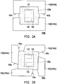
- FIG. 2A is a schematic top view of an electronic device of an embodiment of the disclosure.
- an electronic device 100b is similar to the electronic device 100a of FIG. 1 , and the difference between the two is: in the present embodiment, in consideration of uniformity, a protective structure 140b may be a non-closed structure.
- the protective structure 140b of the present embodiment has a plurality of openings 145b (two openings 145b are schematically shown), and includes a plurality of retaining wall patterns 142b separated from each other (two retaining wall patterns 142b are schematically shown).
- the size of the retaining wall patterns 142b may be the same, and the retaining wall patterns 142b may be in a mirror structure, but the disclosure is not limited thereto.
- the openings 145b are located between the retaining wall patterns 142b, wherein the shape of the openings 145b is, for example, a rectangle, and a portion of the underfill layer 130b is extended into the openings 145b.
- the design of the openings 145b also has the function of exhausting the air existing in the underfill layer 130b.
- FIG. 2B is a schematic top view of an electronic device of another embodiment of the disclosure.
- an electronic device 100c is similar to the electronic device 100b of FIG. 2A , and the differences between the two are: in the present embodiment, a protective structure 140c has four openings 145c and includes four retaining wall patterns 142c separated from each other. The size of the retaining wall patterns 142c may be the same, wherein the four retaining wall patterns 142c are arranged to be, for example, a swastika ( ), but the disclosure is not limited thereto.
- the openings 145c are located between the retaining wall patterns 142c, wherein the diameter of the openings 145c is gradually increased from adjacent to the underfill layer 130b to the direction away from the underfill layer 130b to form, for example, a trapezoid shape, and a portion of the underfill layer 130b is extended into the openings 145c.
- the design of the openings 145c also has the function of exhausting the air existing in the underfill layer 130b.
- the plurality of retaining wall patterns of the protective structure may also have different sizes.
- the shapes of these retaining wall patterns may also be different and asymmetrical, which still falls within the scope of the disclosure.
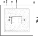
- FIG. 3 is a schematic top view of an electronic device of another embodiment of the disclosure.
- an electronic device 100d is similar to the electronic device 100a of FIG. 1 , and the difference between the two is: in the present embodiment, when the thickness of a protective structure 140d is insufficient, the electronic device 100d further includes a metal layer 160 disposed on the substrate 110 and located between the protective structure 140d and the substrate 110, in order to avoid overflow of the underfill layer 130d.
- the orthographic projection of the protective structure 140d on the substrate 110 is completely overlapped with the orthographic projection of the metal layer 160 on the substrate 110, wherein the orthographic projection of the metal layer 160 on the substrate 110 is less than the orthographic projection of the protective structure 140d on the substrate 110, but the disclosure is not limited thereto.
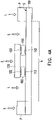
- FIG. 4A to FIG. 4C are schematic cross-sectional views of a manufacturing method of an electronic device of an embodiment of the disclosure.
- the substrate 110 is provided, wherein the substrate 110 includes the first pads 112 thereon.
- the electronic element 120 is bonded on the substrate 110, wherein the electronic element 120 includes the second pads 122, and the first pads 112 and the second pads 122 are structurally and electrically connected together via the solder balls 150.
- a steel plate P is disposed on a portion of the surface S of the substrate 110, wherein the steel plate P surrounds the periphery of the electronic element 120.
- the electronic element 120 and the substrate 110 exposed to the outside of the steel plate P are irradiated with an energy beam L.
- the energy beam L is, for example, extreme ultraviolet (EUV) or plasma that may effectively reduce the contact angle of the substrate 110, in order to increase the wettability of the subsequent underfill layer 130a (please refer to FIG. 4C ).
- EUV extreme ultraviolet
- the steel plate P is removed to define the confinement region A on the substrate 110.
- the step of defining the confinement region A of the substrate 110 in the present embodiment is to treat the surface S of the substrate 110 via the energy beam L, so as to perform surface modification on a partial area of the substrate 110 (i.e., the confinement region A).
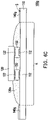
- the underfill layer 130a is formed on the substrate 110, wherein the underfill layer 130a may readily flow to the confinement region A via the siphon phenomenon in order to cover the first pads 112, the second pads 122, and the solder balls 150, and the underfill layer 130a does not flow to a region without surface modification (i.e., the region other than the confinement region A).
- the manufacture of an electronic device 100e is completed.
- FIG. 5A to FIG. 5B are schematic cross-sectional views of some of the steps of a manufacturing method of an electronic device of another embodiment of the disclosure.
- a substrate 110f is provided, wherein the substrate 110f includes the first pads 112 thereon.
- a portion of the substrate 110f is covered with photoresist.
- surface treatment is performed on the substrate 110f by means of plasma, sandblasting, or etching, so as to form a surface roughness structure R in the region of the substrate 110f not covered with photoresist, so as to define the confinement region A of the substrate 110f.
- the photoresist is removed, and the electronic element 120 is bonded on the substrate 110, wherein the electronic element 120 includes the second pads 122, and the first pads 112 and the second pads 122 are structurally and electrically connected together via the solder balls 150.
- the underfill layer 130a is formed on the substrate 110f, wherein the underfill layer 130a may readily flow to the confinement region A via the siphon phenomenon in order to cover the first pads 112, the second pads 122, and the solder balls 150 and be cured, and the underfill layer 130a does not flow on the surface roughness structure R.
- the manufacture of an electronic device 100f is completed.
- the flow range of the underfill layer 130a may be limited by roughening the surface of a region where the underfill layer 130a is not needed, so as to control the area of the underfill layer 130a.
- the surface roughness structure R may also be replaced by a plurality of microstructures separated from each other.
- a substrate is provided.
- a portion of the substrate is covered with photoresist, and microstructures are manufactured via steps such as lithography, so as to define a confinement region of the substrate.
- an electronic element is bonded on the substrate.
- an underfill layer is formed on the substrate, wherein the underfill layer may readily flow to the confinement region via the siphon phenomenon to be cured, and the underfill layer does not flow on the microstructures. At this point, the manufacture of the electronic device is completed.
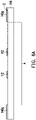
- FIG. 6A to FIG. 6C are schematic cross-sectional views of a manufacturing method of an electronic device of another embodiment of the disclosure.
- the substrate 110 is provided, wherein the substrate 110 includes the first pads 112 thereon.
- a fluorine-containing substance is coated on the substrate 110 via screen printing.
- the fluorine-containing substance is dried to dehydrate the surface S of the substrate 110 and the fluorine-containing substance to generate a Si-O bond to form a hydrophobic protective structure 140g, and the protective structure 140g defines the confinement region A of the substrate 110.
- FIG. 6A the substrate 110 is provided, wherein the substrate 110 includes the first pads 112 thereon.
- a fluorine-containing substance is coated on the substrate 110 via screen printing.
- the fluorine-containing substance is dried to dehydrate the surface S of the substrate 110 and the fluorine-containing substance to generate a Si-O bond to form a hydrophobic protective structure 140g, and the protective structure 140g defines the confinement region A of the substrate 110.
- the electronic element 120 is bonded on the substrate 110, wherein the electronic element 120 includes the second pads 122, and the first pads 112 and the second pads 122 are structurally and electrically connected together via the solder balls 150.
- the underfill layer 130a is formed on the substrate 110, wherein the underfill layer 130a may readily flow to the confinement region A via the siphon phenomenon in order to cover the first pads 112, the second pads 122, and the solder balls 150 and be cured, and the underfill layer 130a does not flow on the protective structure 140g.
- the manufacture of an electronic device 100g is completed.
- the protective structure 140g having hydrophobicity is formed, so that the underfill layer 130a is not wetted by the protective structure 140g. Thereby, the flow range of the underfill layer 130a is limited, so as to control the area of the underfill layer 130a.
- the fluorine-containing substance may also be replaced by a polymer, such as a fluorocarbon polymer.
- a substrate is provided.
- chlorofluorocarbon (C 4 F 8 ) as the reactive gas
- a fluorocarbon polymer thin film is formed on the substrate by inductively coupled plasma chemical vapor deposition (ICP-CVD) at room temperature, wherein the fluorocarbon polymer thin film covers the entire surface of the substrate.
- ICP-CVD inductively coupled plasma chemical vapor deposition
- the fluorocarbon polymer thin film is patterned by lithography to form a hydrophobic protective structure and define a confinement region of the substrate. That is, in addition to fluorocarbon chains reducing surface energy, silanes may also be used to form a hydrophobic surface.
- an electronic element is bonded on the substrate.
- an underfill layer is formed on the substrate, wherein the underfill layer may readily flow in the confinement region via the siphon phenomenon to be cured, and the underfill layer does not flow on the protective structure. At this point, the manufacture of the electronic device is completed.
- the protective structure is disposed on the substrate and adjacent to the underfill layer, thereby limiting the scope of the underfill layer, so that the electronic device of the disclosure may effectively control the area of the underfill layer.
- the amount and shape of the underfill layer may be consistent.
Landscapes
- Structures Or Materials For Encapsulating Or Coating Semiconductor Devices Or Solid State Devices (AREA)
- Encapsulation Of And Coatings For Semiconductor Or Solid State Devices (AREA)
Abstract
Description
- The disclosure relates to an electronic device and a manufacturing method thereof, and more particularly, to an electronic device and a manufacturing method thereof that may effectively control the area of an underfill layer.
- In general, after an electronic element is bonded to the substrate, an underfill process is performed, so as to allow an underfill layer to enter the gap between the electronic element and the substrate via the siphon phenomenon by means of a jetting process or a dispensing process on the outside of the junction of the electronic element and the substrate, in order to cover the pads and solder balls and fix the relative position between the electronic element and the substrate. However, the underfill layer is free-flowing on the substrate, and therefore it is difficult to control the area thereof, resulting in material waste, and even causing the phenomenon of capacitance/inductance/electromagnetic interference.
- The disclosure is directed to an electronic device and a manufacturing method thereof that may effectively control the area of an underfill layer.
- According to an embodiment of the disclosure, an electronic device includes a substrate, an electronic element, an underfill layer, and a protective structure. The electronic element is disposed on the substrate. At least a portion of the underfill layer is disposed between the substrate and the electronic element. A thickness of the underfill layer is not greater than a height from a surface of the substrate to an upper surface of the electronic element. The protective structure is disposed on the substrate and adjacent to the underfill layer.
- According to an embodiment of the disclosure, a manufacturing method of an electronic device includes the following steps. A substrate is provided. A confinement region of the substrate is defined. An electronic element is bonded on the substrate. An underfill layer is formed on the substrate.
- Based on the above, in an embodiment of the disclosure, the protective structure is disposed on the substrate and adjacent to the underfill layer, thereby limiting the scope of the underfill layer, so that the electronic device of the disclosure may effectively control the area of the underfill layer. Thus, the amount and shape of the underfill layer may be consistent.
- In order to make the above features and advantages of the disclosure better understood, embodiments are specifically provided below with reference to figures for detailed description as follows.
-
-
FIG. 1 is a schematic cross-sectional view of an electronic device of an embodiment of the disclosure. -
FIG. 2A is a schematic top view of an electronic device of an embodiment of the disclosure. -
FIG. 2B is a schematic top view of an electronic device of another embodiment of the disclosure. -
FIG. 3 is a schematic top view of an electronic device of another embodiment of the disclosure. -
FIG. 4A to FIG. 4C are schematic cross-sectional views of a manufacturing method of an electronic device of an embodiment of the disclosure. -
FIG. 5A to FIG. 5B are schematic cross-sectional views of some of the steps of a manufacturing method of an electronic device of another embodiment of the disclosure. -
FIG. 6A to FIG. 6C are schematic cross-sectional views of a manufacturing method of an electronic device of another embodiment of the disclosure. - The disclosure may be understood by referring to the following detailed description in conjunction with the accompanying drawings. It should be noted that in order to facilitate understanding to the reader and to simplify the drawings, the multiple drawings in the disclosure depict a part of the electronic device, and certain elements in the drawings are not drawn to actual scale. In addition, the number and size of each element in the figures are for illustration, and are not intended to limit the scope of the disclosure.
- Certain terms are used throughout the specification and the appended claims of the disclosure to refer to particular elements. Those skilled in the art should understand that electronic equipment manufacturers may refer to the same elements under different names. This article is not intended to distinguish between elements having the same function but different names.
- In the following description and claims, the words "including" and "containing" and the like are open words, so they should be interpreted as meaning "including but not limited to..."
- Moreover, relative terms, such as "below" or "bottom" and "above" or "top," may be used in the embodiments to describe the relative relationship of one element of the drawings to another element. It will be understood that if the device in the figures were turned upside down, elements described on the "lower" side would become elements described on the "upper" side.
- In some embodiments of the disclosure, terms such as "connection", "interconnection", etc., regarding bonding and connection, unless specifically defined, may mean that two structures are in direct contact, or that two structures are not in direct contact (indirect contact) and there are other structures located between these two structures. Moreover, the terms of bonding and connecting may also include the case where both structures are movable or both structures are fixed. Moreover, the term "coupled" includes the transfer of energy between two structures by means of direct or indirect electrical connection, or the transfer of energy by means of mutual induction between two separate structures.
- It should be understood that when an element or film layer is referred to as "on" or "connected to" to another element or film layer, the element or film layer may be directly on the other element or film layer or directly connected to the other element or film layer, or there is an inserted element or film layer between the two (indirect case). Conversely, when an element is referred to as "directly" on or "directly connected" to another element or film layer, there is no intervening element or film layer between the two.
- The terms "about", "equal to", "equal" or "identical", "substantially" or "roughly" are generally interpreted as being within 20% of a given value or range, or interpreted as being within 10%, 5%, 3%, 2%, 1%, or 0.5% of a given value or range.
- As used herein, the terms "film" and/or "layer" may refer to any continuous or discontinuous structure and material (such as a material deposited by a method disclosed herein). For example, the film and/or layer may include a two-dimensional material, a three-dimensional material, a nanoparticle, or even a partial or complete molecular layer, or a partial or complete atomic layer, or a cluster of atoms and/or molecules. The film or layer may include a material or layer having a pinhole, which may be at least partially continuous.
- Although the terms first, second, third...may be used to describe various constituent elements, the constituent elements are not limited to these terms. These terms are used to distinguish a single constituent element from other constituent elements in the specification. The same terms may not be used in the claims, and the elements in the claims may be replaced with first, second, third...according to the order declared by the elements in the claims. Therefore, in the following description, the first constituent element may be the second constituent element in the claims.
- Unless otherwise defined, all terms (including technical and scientific terms) used herein have the same meaning as commonly understood by one of ordinary skill in the art to which this disclosure belongs. It should be understood that, these terms, such as those defined in commonly used dictionaries, should be interpreted as having meaning consistent with the relevant technique and the background or context of the disclosure, and should not be interpreted in an idealized or excessively formal way, unless specifically defined.
- It should be noted that in the following embodiments, the technical features in several different embodiments may be replaced, recombined, and mixed to complete other embodiments without departing from the spirit of the disclosure.
- An electronic device of disclosure may include a display device, antenna device, sensing device, light-emitting device, and/or tiling device, but the disclosure is not limited thereto. The electronic device may include a bendable or flexible electronic device. The electronic device may include an electronic element. The electronic element may include a passive element and an active element, such as a capacitor, resistor, inductor, variable capacitor, filter, diode, transistor, sensor, microelectromechanical system (MEMS), liquid-crystal chip, etc., but the disclosure is not limited thereto. The diode may include a light-emitting diode or a photodiode. The light-emitting diode may include, for example, an organic light-emitting diode (OLED), a mini LED, micro LED, or quantum dot light-emitting diode, fluorescence, phosphor, or other suitable materials, or a combination of the above, but the disclosure is not limited thereto. The sensor may include, for example, a capacitive sensor, optical sensor, electromagnetic sensor, fingerprint sensor (FPS), touch sensor, antenna, or pen sensor, but the disclosure is not limited thereto. The following adopts a display device as an electronic device to explain the content of the disclosure, but the disclosure is not limited thereto.
- Hereinafter, reference will be made in detail to exemplary embodiments of the disclosure, and examples of the exemplary embodiments are illustrated in the figures. Wherever possible, the same reference numerals are used in the figures and the descriptions to refer to the same or similar portions.
-
FIG. 1 is a schematic cross-sectional view of an electronic device of an embodiment of the disclosure. Referring toFIG. 1 , in the present embodiment, anelectronic device 100a includes asubstrate 110, anelectronic element 120, anunderfill layer 130a, and aprotective structure 140a. Theelectronic element 120 is disposed on thesubstrate 110. At least a portion of theunderfill layer 130a is disposed between thesubstrate 110 and theelectronic element 120. A thickness T of theunderfill layer 130a is not greater than a height H from a surface S of thesubstrate 110 to anupper surface 121 of theelectronic element 120. Theprotective structure 140a is disposed on thesubstrate 110 and adjacent to theunderfill layer 130a. - Specifically, in the present embodiment, the
substrate 110 is, for example, a glass substrate, a glass fiber (FR4) substrate, a flexible plastic substrate, a thin-film substrate, a flexible substrate, or other suitable substrates, but the disclosure is not limited thereto. A thin-film transistor or other driving circuits may be disposed on the substrate. Thesubstrate 110 includes a plurality offirst pads 112 separated from each other, wherein thefirst pads 112 may be disposed on the surface S of thesubstrate 110, but the disclosure is not limited thereto. In another embodiment, the surface of the substrate has a concave portion, and thefirst pads 112 may also be disposed in the concave portion, which still belongs to the scope of the disclosure. - The
electronic element 120 is, for example, an LED chip that may be a chip made of silicon (Si), gallium arsenide (GaAs), gallium nitride (GaN), silicon carbide (SiC), sapphire, or a glass substrate, but the disclosure is not limited thereto. In another embodiment, theelectronic element 120 may also be a semiconductor package element, such as a ball grid array (BGA) package element, a chip size package (CSP) element, a flip-chip or 2.5D/3D semiconductor package element, but the disclosure is not limited thereto. In another embodiment, theelectronic element 120 may also be any kind of chip, such as an integrated circuit (IC), transistor, silicon-controlled rectifier, valve, thin-film transistor, capacitor, inductor, variable capacitor, filter, resistor, diode, MEMS, liquid-crystal chip, etc., but the disclosure is not limited thereto. Theelectronic element 120 includes a plurality ofsecond pads 122 separated from each other, wherein thefirst pads 112 and thesecond pads 122 are structurally and electrically connected together via a plurality ofsolder balls 150. That is, theelectronic element 120 of the present embodiment is, for example, flip-chip bonded on thesubstrate 110. - As shown in
FIG. 1 , theunderfill layer 130a is disposed between thesubstrate 110 and theelectronic element 120 and covers thefirst pads 112, thesecond pads 122, and thesolder balls 150. Theunderfill layer 130a may be configured to increase the adhesion between theelectronic element 120 and thesubstrate 110, and may fix the relative positions of thefirst pads 112, thesolder balls 150, and thesecond pads 122. In an embodiment, in the case where theelectronic device 100a is, for example, an antenna device or a sensing device, when the thickness T of theunderfill layer 130a is not greater than the height H from the surface S of thesubstrate 110 to theupper surface 121 of theelectronic element 120, a high-frequency signal may be allowed to pass through and the loss of the high-frequency signal may be reduced. In another embodiment not shown, to further reduce the amount of signal loss, the thickness of the underfill layer below the electronic element may be less than the height from the surface of the substrate to the lower surface of the electronic element. In another embodiment not shown, the underfill layer may also completely cover the electronic element, and in the case of an electronic element such as an LED, the electronic device may have better light pattern and light focusing effect. - Moreover, the disposition of the
protective structure 140a of the present embodiment may define a confinement region A on thesubstrate 110, wherein theprotective structure 140a is, for example, a closed structure, such as a continuous mountain-shaped dam or a continuous wall that may surround theunderfill layer 130a to limit the region of theunderfill layer 130a. In other words, theunderfill layer 130a is confined to be located in the confinement region A. In an embodiment, the material of theprotective structure 140a may be, for example, an organic material, but the disclosure is not limited thereto. The top view shape of theprotective structure 140a may be, for example, a hollow rectangle, and the thickness of theprotective structure 140a may be, for example, 1 micrometer (µm) to 100 µm, but the disclosure is not limited thereto. - In manufacture, please refer to
FIG. 1 again. First, thesubstrate 110 is provided, wherein thesubstrate 110 includes thefirst pads 112. The material of thefirst pads 112 may be electroless nickel immersion gold (abbreviated as ENIG) or other conductive materials. Next, theprotective structure 140a is formed on thesubstrate 110 to define the confinement region A of thesubstrate 110. Next, theelectronic element 120 is bonded on thesubstrate 110, wherein theelectronic element 120 includes thesecond pads 122, and the material of thesecond pads 122 may be ENIG or other conductive materials. Thefirst pads 112 and thesecond pads 122 are structurally and electrically connected together via the plurality ofsolder balls 150. It should be noted that the disclosure does not limit the sequence of forming theprotective structure 140a on thesubstrate 110 and bonding theelectronic element 120 on thesubstrate 110. In other words, theprotective structure 140a may be formed on thesubstrate 110 first, and then theelectronic element 120 is bonded on thesubstrate 110; alternatively, theelectronic element 120 is bonded on thesubstrate 110 first, and then theprotective structure 140a is formed on thesubstrate 110. Lastly, theunderfill layer 130a is formed on thesubstrate 110, wherein theunderfill layer 130a is disposed between thesubstrate 110 and theelectronic element 120 and covers thefirst pads 112, thesecond pads 122, and thesolder balls 150. At this point, the manufacture of anelectronic device 100a is completed. - In short, the
protective structure 140a of the present embodiment may limit the area of theunderfill layer 130a, so that the amount and shape of theunderfill layer 130a are consistent. Considering theelectronic device 100a applied to high-frequency transmission, the material loss of the high-frequency signal in theelectronic device 100a needs to be consistent. In other words, in the present embodiment, theprotective structure 140a is provided to adjust/limit the amount of theunderfill layer 130a, so that theelectronic device 100a of the present embodiment may effectively control the area of theunderfill layer 130a. - It must be noted here that the following embodiments adopt the reference numerals and part of the content of the above embodiments, wherein the same reference numerals are used to represent the same or similar elements, and the description of the same technical content is omitted. For the description of the omitted parts, reference may be made to the above embodiments, which is not repeated in the following embodiments.
-
FIG. 2A is a schematic top view of an electronic device of an embodiment of the disclosure. Please refer toFIG. 1 andFIG. 2A at the same time, anelectronic device 100b is similar to theelectronic device 100a ofFIG. 1 , and the difference between the two is: in the present embodiment, in consideration of uniformity, aprotective structure 140b may be a non-closed structure. Specifically, theprotective structure 140b of the present embodiment has a plurality ofopenings 145b (twoopenings 145b are schematically shown), and includes a plurality of retainingwall patterns 142b separated from each other (two retainingwall patterns 142b are schematically shown). The size of the retainingwall patterns 142b may be the same, and the retainingwall patterns 142b may be in a mirror structure, but the disclosure is not limited thereto. Theopenings 145b are located between the retainingwall patterns 142b, wherein the shape of theopenings 145b is, for example, a rectangle, and a portion of theunderfill layer 130b is extended into theopenings 145b. In addition to accommodating the overflowing adhesive, the design of theopenings 145b also has the function of exhausting the air existing in theunderfill layer 130b. -
FIG. 2B is a schematic top view of an electronic device of another embodiment of the disclosure. Please refer toFIG. 2A and FIG. 2B at the same time, anelectronic device 100c is similar to theelectronic device 100b ofFIG. 2A , and the differences between the two are: in the present embodiment, aprotective structure 140c has fouropenings 145c and includes four retainingwall patterns 142c separated from each other. The size of the retainingwall patterns 142c may be the same, wherein the fourretaining wall patterns 142c are arranged to be, for example, a swastika (), but the disclosure is not limited thereto. The
openings 145c are located between the retainingwall patterns 142c, wherein the diameter of theopenings 145c is gradually increased from adjacent to theunderfill layer 130b to the direction away from theunderfill layer 130b to form, for example, a trapezoid shape, and a portion of theunderfill layer 130b is extended into theopenings 145c. In addition to accommodating the overflowing adhesive, the design of theopenings 145c also has the function of exhausting the air existing in theunderfill layer 130b. - In another embodiment not shown, considering wetting conditions, the plurality of retaining wall patterns of the protective structure may also have different sizes. Alternatively, the shapes of these retaining wall patterns may also be different and asymmetrical, which still falls within the scope of the disclosure.
-
FIG. 3 is a schematic top view of an electronic device of another embodiment of the disclosure. Please refer toFIG. 1 andFIG. 3 at the same time, anelectronic device 100d is similar to theelectronic device 100a ofFIG. 1 , and the difference between the two is: in the present embodiment, when the thickness of aprotective structure 140d is insufficient, theelectronic device 100d further includes ametal layer 160 disposed on thesubstrate 110 and located between theprotective structure 140d and thesubstrate 110, in order to avoid overflow of theunderfill layer 130d. In an embodiment, the orthographic projection of theprotective structure 140d on thesubstrate 110 is completely overlapped with the orthographic projection of themetal layer 160 on thesubstrate 110, wherein the orthographic projection of themetal layer 160 on thesubstrate 110 is less than the orthographic projection of theprotective structure 140d on thesubstrate 110, but the disclosure is not limited thereto. -
FIG. 4A to FIG. 4C are schematic cross-sectional views of a manufacturing method of an electronic device of an embodiment of the disclosure. First, referring toFIG. 4A , thesubstrate 110 is provided, wherein thesubstrate 110 includes thefirst pads 112 thereon. Next, theelectronic element 120 is bonded on thesubstrate 110, wherein theelectronic element 120 includes thesecond pads 122, and thefirst pads 112 and thesecond pads 122 are structurally and electrically connected together via thesolder balls 150. Next, a steel plate P is disposed on a portion of the surface S of thesubstrate 110, wherein the steel plate P surrounds the periphery of theelectronic element 120. Next, theelectronic element 120 and thesubstrate 110 exposed to the outside of the steel plate P are irradiated with an energy beam L. Here, the energy beam L is, for example, extreme ultraviolet (EUV) or plasma that may effectively reduce the contact angle of thesubstrate 110, in order to increase the wettability of thesubsequent underfill layer 130a (please refer toFIG. 4C ). Next, referring toFIG. 4B , the steel plate P is removed to define the confinement region A on thesubstrate 110. In other words, the step of defining the confinement region A of thesubstrate 110 in the present embodiment is to treat the surface S of thesubstrate 110 via the energy beam L, so as to perform surface modification on a partial area of the substrate 110 (i.e., the confinement region A). Lastly, referring toFIG. 4B andFIG. 4C at the same time, theunderfill layer 130a is formed on thesubstrate 110, wherein theunderfill layer 130a may readily flow to the confinement region A via the siphon phenomenon in order to cover thefirst pads 112, thesecond pads 122, and thesolder balls 150, and theunderfill layer 130a does not flow to a region without surface modification (i.e., the region other than the confinement region A). At this point, the manufacture of anelectronic device 100e is completed. -
FIG. 5A to FIG. 5B are schematic cross-sectional views of some of the steps of a manufacturing method of an electronic device of another embodiment of the disclosure. First, referring toFIG. 5A , asubstrate 110f is provided, wherein thesubstrate 110f includes thefirst pads 112 thereon. Next, a portion of thesubstrate 110f is covered with photoresist. Next, surface treatment is performed on thesubstrate 110f by means of plasma, sandblasting, or etching, so as to form a surface roughness structure R in the region of thesubstrate 110f not covered with photoresist, so as to define the confinement region A of thesubstrate 110f. Next, the photoresist is removed, and theelectronic element 120 is bonded on thesubstrate 110, wherein theelectronic element 120 includes thesecond pads 122, and thefirst pads 112 and thesecond pads 122 are structurally and electrically connected together via thesolder balls 150. Lastly, referring toFIG. 5A andFIG. 5B at the same time, theunderfill layer 130a is formed on thesubstrate 110f, wherein theunderfill layer 130a may readily flow to the confinement region A via the siphon phenomenon in order to cover thefirst pads 112, thesecond pads 122, and thesolder balls 150 and be cured, and theunderfill layer 130a does not flow on the surface roughness structure R. At this point, the manufacture of anelectronic device 100f is completed. - Since the
underfill layer 130a is not wetted when the roughness is higher, the flow range of theunderfill layer 130a may be limited by roughening the surface of a region where theunderfill layer 130a is not needed, so as to control the area of theunderfill layer 130a. - In another embodiment not shown, the surface roughness structure R may also be replaced by a plurality of microstructures separated from each other. In detail, first, a substrate is provided. Next, a portion of the substrate is covered with photoresist, and microstructures are manufactured via steps such as lithography, so as to define a confinement region of the substrate. Next, an electronic element is bonded on the substrate. Lastly, an underfill layer is formed on the substrate, wherein the underfill layer may readily flow to the confinement region via the siphon phenomenon to be cured, and the underfill layer does not flow on the microstructures. At this point, the manufacture of the electronic device is completed.
-
FIG. 6A to FIG. 6C are schematic cross-sectional views of a manufacturing method of an electronic device of another embodiment of the disclosure. First, referring toFIG. 6A , thesubstrate 110 is provided, wherein thesubstrate 110 includes thefirst pads 112 thereon. Next, a fluorine-containing substance is coated on thesubstrate 110 via screen printing. Next, the fluorine-containing substance is dried to dehydrate the surface S of thesubstrate 110 and the fluorine-containing substance to generate a Si-O bond to form a hydrophobicprotective structure 140g, and theprotective structure 140g defines the confinement region A of thesubstrate 110. Next, referring toFIG. 6B , theelectronic element 120 is bonded on thesubstrate 110, wherein theelectronic element 120 includes thesecond pads 122, and thefirst pads 112 and thesecond pads 122 are structurally and electrically connected together via thesolder balls 150. Lastly, referring toFIG. 6B andFIG. 6C at the same time, theunderfill layer 130a is formed on thesubstrate 110, wherein theunderfill layer 130a may readily flow to the confinement region A via the siphon phenomenon in order to cover thefirst pads 112, thesecond pads 122, and thesolder balls 150 and be cured, and theunderfill layer 130a does not flow on theprotective structure 140g. At this point, the manufacture of anelectronic device 100g is completed. - Since the surface S of the
substrate 110 is coated with the fluorine-containing substance, theprotective structure 140g having hydrophobicity is formed, so that theunderfill layer 130a is not wetted by theprotective structure 140g. Thereby, the flow range of theunderfill layer 130a is limited, so as to control the area of theunderfill layer 130a. - In another embodiment not shown, the fluorine-containing substance may also be replaced by a polymer, such as a fluorocarbon polymer. In detail, first, a substrate is provided. Next, using chlorofluorocarbon (C4F8) as the reactive gas, a fluorocarbon polymer thin film is formed on the substrate by inductively coupled plasma chemical vapor deposition (ICP-CVD) at room temperature, wherein the fluorocarbon polymer thin film covers the entire surface of the substrate. Next, the fluorocarbon polymer thin film is patterned by lithography to form a hydrophobic protective structure and define a confinement region of the substrate. That is, in addition to fluorocarbon chains reducing surface energy, silanes may also be used to form a hydrophobic surface. Next, an electronic element is bonded on the substrate. Lastly, an underfill layer is formed on the substrate, wherein the underfill layer may readily flow in the confinement region via the siphon phenomenon to be cured, and the underfill layer does not flow on the protective structure. At this point, the manufacture of the electronic device is completed.
- Based on the above, in an embodiment of the disclosure, the protective structure is disposed on the substrate and adjacent to the underfill layer, thereby limiting the scope of the underfill layer, so that the electronic device of the disclosure may effectively control the area of the underfill layer. Thus, the amount and shape of the underfill layer may be consistent.
Claims (15)
- An electronic device (100a, 100b, 100c, 100d, 100e, 100f, 100g), comprising:a substrate (110, 110f);an electronic element (120) disposed on the substrate (110, 110f);an underfill layer (130a, 130b, 130d), wherein at least a portion of the underfill layer (130a, 130b, 130d) is disposed between the substrate (110, 110f) and the electronic element (120), and a thickness (T) of the underfill layer (130a, 130b, 130d) is not greater than a height (H) from a surface (S) of the substrate (110, 110f) to an upper surface (121) of the electronic element (120); anda protective structure (140a, 140b,140c,140d,140g) disposed on the substrate (110, 110f) and adjacent to the underfill layer (130a, 130b, 130d).
- The electronic device (100a, 100b, 100c, 100d, 100e, 100f, 100g) of claim 1, wherein the protective structure (140a, 140b,140c,140d,140g) surrounds the underfill layer (130a, 130b, 130d).
- The electronic device (100a) of claim 2, wherein a shape of the protective structure (140a) comprises a continuous gabled dam or a continuous retaining wall.
- The electronic device (100b, 100c) of claim 1, wherein the protective structure (140b, 140c) comprises a plurality of retaining wall patterns (142b, 142c).
- The electronic device (100b, 100c) of claim 4, wherein the protective structure (140b,140c) has a plurality of openings (145b, 145c), the plurality of openings (145b, 145c) are located between the plurality of retaining wall patterns (142b, 142c), and a portion of the underfill layer (130b) is extended into the plurality of openings (145b, 145c).
- The electronic device (100b, 100c) of claim 5, wherein a diameter of the plurality of openings (145b, 145c) is gradually increased from adjacent to the underfill layer(130b) to a direction away from the underfill layer (130b).
- The electronic device (100g) of claim 1, wherein the protective structure (140g) comprises a fluorine-containing substance.
- The electronic device (100g) of claim 1, wherein the protective structure (140g) comprises a polymer.
- The electronic device (100g) of claim 8, wherein the protective structure (140g) comprises a fluorocarbon polymer.
- The electronic device (100d) of claim 1, further comprising:
a metal layer (160) disposed on the substrate (110) and located between the protective structure (140d) and the substrate (110). - A manufacturing method of an electronic device (100a, 100b, 100c, 100d, 100e, 100f, 100g), comprising:providing a substrate (110, 110f);defining a confinement region (A) of the substrate (110, 110f);bonding an electronic element (120) on the substrate (110, 110f); andforming an underfill layer (130a, 130b, 130d) on the substrate (110, 110f), wherein a thickness (T) of the underfill layer (130a, 130b, 130d) is not greater than a height (H) from a surface (S) of the substrate (110, 1 10f) to an upper surface (121) of the electronic element (120).
- The manufacturing method of the electronic device (100a, 100b, 100c, 100d) of claim 11, wherein the step of defining the confinement region (A) of the substrate (110) is forming a protective structure (140a,140b,140c) on the substrate (110).
- The manufacturing method of the electronic device (100g) of claim 12 wherein the protective structure (140g) comprises a fluorine-containing substance or a polymer.
- The manufacturing method of the electronic device (100e, 100f, 100g) of claim 11, wherein the step of defining the confinement region (A) of the substrate (110, 110f) is treating the surface (S) of the substrate (110, 110f).
- The manufacturing method of the electronic device (100e, 100f, 100g) of claim 14, wherein treating the surface (S) of the substrate (110, 110f) is treating the surface (S) of the substrate (110, 110f) via an energy beam (L) to perform a surface modification on the confinement region (A) of the substrate (110, 110f).
Applications Claiming Priority (2)
| Application Number | Priority Date | Filing Date | Title |
|---|---|---|---|
| US202163219831P | 2021-07-09 | 2021-07-09 | |
| CN202210258940.5A CN115602638A (en) | 2021-07-09 | 2022-03-16 | Electronic device and manufacturing method thereof |
Publications (2)
| Publication Number | Publication Date |
|---|---|
| EP4117025A2 true EP4117025A2 (en) | 2023-01-11 |
| EP4117025A3 EP4117025A3 (en) | 2023-05-24 |
Family
ID=83049872
Family Applications (1)
| Application Number | Title | Priority Date | Filing Date |
|---|---|---|---|
| EP22180360.4A Pending EP4117025A3 (en) | 2021-07-09 | 2022-06-22 | Underfilled electronic device and manufacturing method thereof |
Country Status (2)
| Country | Link |
|---|---|
| US (1) | US12610842B2 (en) |
| EP (1) | EP4117025A3 (en) |
Family Cites Families (11)
| Publication number | Priority date | Publication date | Assignee | Title |
|---|---|---|---|---|
| US6048656A (en) * | 1999-05-11 | 2000-04-11 | Micron Technology, Inc. | Void-free underfill of surface mounted chips |
| US20080067502A1 (en) | 2006-09-14 | 2008-03-20 | Nirupama Chakrapani | Electronic packages with fine particle wetting and non-wetting zones |
| JP4441545B2 (en) * | 2007-03-30 | 2010-03-31 | Okiセミコンダクタ株式会社 | Semiconductor device |
| TWI394235B (en) | 2008-04-24 | 2013-04-21 | 欣興電子股份有限公司 | Package substrate and its preparation method |
| KR101054440B1 (en) * | 2009-04-27 | 2011-08-05 | 삼성전기주식회사 | Electronic device package and manufacturing method thereof |
| KR20140019688A (en) * | 2012-08-07 | 2014-02-17 | 삼성전기주식회사 | Flat dam and method for manufacturing chip package using the same |
| US20140048934A1 (en) | 2012-08-15 | 2014-02-20 | Taiwan Semiconductor Manufacturing Company, Ltd. | Method to control underfill fillet width |
| US9224673B2 (en) * | 2013-03-08 | 2015-12-29 | Taiwan Semiconductor Manufacturing Company, Ltd. | Packages for semiconductor devices, packaged semiconductor devices, and methods of cooling packaged semiconductor devices |
| TWI736802B (en) | 2018-10-23 | 2021-08-21 | 矽品精密工業股份有限公司 | Electronic package |
| US10529637B1 (en) | 2018-10-31 | 2020-01-07 | Taiwan Semiconductor Manufacturing Company, Ltd. | Integrated circuit package and method of forming same |
| US10629455B1 (en) * | 2018-11-20 | 2020-04-21 | Nanya Technology Corporation | Semiconductor package having a blocking dam |
-
2022
- 2022-06-21 US US17/845,929 patent/US12610842B2/en active Active
- 2022-06-22 EP EP22180360.4A patent/EP4117025A3/en active Pending
Also Published As
| Publication number | Publication date |
|---|---|
| US20230009495A1 (en) | 2023-01-12 |
| US12610842B2 (en) | 2026-04-21 |
| EP4117025A3 (en) | 2023-05-24 |
Similar Documents
| Publication | Publication Date | Title |
|---|---|---|
| CN102263117B (en) | Chip package and method for forming the same | |
| US8227927B2 (en) | Chip package and fabrication method thereof | |
| CN109119410B (en) | Method for manufacturing light emitting device | |
| CN102388469B (en) | Manufacture of compact optoelectronic component packages | |
| US8431479B2 (en) | Semiconductor devices having redistribution structures and packages, and methods of forming the same | |
| US20160111616A1 (en) | Wafer level packaging of electronic device | |
| CN104377217B (en) | The packaging part of imaging sensor and the method for packing of imaging sensor | |
| US12610842B2 (en) | Electronic device including an underfill layer and a protective structure adjacent to the underfill layer | |
| US20090102056A1 (en) | Patterned Leads For WLCSP And Method For Fabricating The Same | |
| TWI803242B (en) | Electronic device and manufacturing method thereof | |
| TWI718415B (en) | Substrate structure and electronic device | |
| CN110349935B (en) | Semiconductor substrate, semiconductor packaging structure, and method for manufacturing semiconductor device | |
| CN104360583B (en) | Image processing-based lithography system and target object coating method | |
| Fukushima et al. | 3-D sidewall interconnect formation climbing over self-assembled KGDs for large-area heterogeneous integration | |
| TWI819456B (en) | Composite layer circuit element and manufacturing method thereof | |
| CN101996978A (en) | Chip package and method for forming the same | |
| US20250046694A1 (en) | Electronic device and manufacturing method of electronic device | |
| CN102811548B (en) | Circuit structure and its manufacturing method | |
| US20250301571A1 (en) | Electronic device and manufacturing method thereof | |
| EP1676471B1 (en) | Electronic device and method of manufacturing thereof | |
| US20240387337A1 (en) | Electronic device and manufacturing method thereof | |
| US20250379159A1 (en) | Electronic device | |
| TW202507951A (en) | Electronic device and manufacturing method of electronic device | |
| TWI913587B (en) | Electronic device and manufacturing method thereof | |
| TWI919216B (en) | Method for processing an optoelectronic arrangement and optoelectronic arrangement |
Legal Events
| Date | Code | Title | Description |
|---|---|---|---|
| PUAI | Public reference made under article 153(3) epc to a published international application that has entered the european phase |
Free format text: ORIGINAL CODE: 0009012 |
|
| STAA | Information on the status of an ep patent application or granted ep patent |
Free format text: STATUS: THE APPLICATION HAS BEEN PUBLISHED |
|
| AK | Designated contracting states |
Kind code of ref document: A2 Designated state(s): AL AT BE BG CH CY CZ DE DK EE ES FI FR GB GR HR HU IE IS IT LI LT LU LV MC MK MT NL NO PL PT RO RS SE SI SK SM TR |
|
| PUAL | Search report despatched |
Free format text: ORIGINAL CODE: 0009013 |
|
| AK | Designated contracting states |
Kind code of ref document: A3 Designated state(s): AL AT BE BG CH CY CZ DE DK EE ES FI FR GB GR HR HU IE IS IT LI LT LU LV MC MK MT NL NO PL PT RO RS SE SI SK SM TR |
|
| RIC1 | Information provided on ipc code assigned before grant |
Ipc: H01L 33/52 20100101ALN20230418BHEP Ipc: H01L 21/56 20060101AFI20230418BHEP |
|
| STAA | Information on the status of an ep patent application or granted ep patent |
Free format text: STATUS: REQUEST FOR EXAMINATION WAS MADE |
|
| 17P | Request for examination filed |
Effective date: 20231115 |
|
| RBV | Designated contracting states (corrected) |
Designated state(s): AL AT BE BG CH CY CZ DE DK EE ES FI FR GB GR HR HU IE IS IT LI LT LU LV MC MK MT NL NO PL PT RO RS SE SI SK SM TR |