EP4116975A1 - Adaptive word line underdrive control for an in-memory compute operation where simultaneous access is made to plural rows of a static random access memory (sram) - Google Patents
Adaptive word line underdrive control for an in-memory compute operation where simultaneous access is made to plural rows of a static random access memory (sram) Download PDFInfo
- Publication number
- EP4116975A1 EP4116975A1 EP22182469.1A EP22182469A EP4116975A1 EP 4116975 A1 EP4116975 A1 EP 4116975A1 EP 22182469 A EP22182469 A EP 22182469A EP 4116975 A1 EP4116975 A1 EP 4116975A1
- Authority
- EP
- European Patent Office
- Prior art keywords
- circuit
- memory
- voltage
- word line
- current
- Prior art date
- Legal status (The legal status is an assumption and is not a legal conclusion. Google has not performed a legal analysis and makes no representation as to the accuracy of the status listed.)
- Granted
Links
Images



Classifications
-
- G—PHYSICS
- G11—INFORMATION STORAGE
- G11C—STATIC STORES
- G11C11/00—Digital stores characterised by the use of particular electric or magnetic storage elements; Storage elements therefor
- G11C11/21—Digital stores characterised by the use of particular electric or magnetic storage elements; Storage elements therefor using electric elements
- G11C11/34—Digital stores characterised by the use of particular electric or magnetic storage elements; Storage elements therefor using electric elements using semiconductor devices
- G11C11/40—Digital stores characterised by the use of particular electric or magnetic storage elements; Storage elements therefor using electric elements using semiconductor devices using transistors
- G11C11/401—Digital stores characterised by the use of particular electric or magnetic storage elements; Storage elements therefor using electric elements using semiconductor devices using transistors forming cells needing refreshing or charge regeneration, i.e. dynamic cells
- G11C11/4063—Auxiliary circuits, e.g. for addressing, decoding, driving, writing, sensing or timing
- G11C11/407—Auxiliary circuits, e.g. for addressing, decoding, driving, writing, sensing or timing for memory cells of the field-effect type
- G11C11/408—Address circuits
- G11C11/4085—Word line control circuits, e.g. word line drivers, - boosters, - pull-up, - pull-down, - precharge
-
- G—PHYSICS
- G11—INFORMATION STORAGE
- G11C—STATIC STORES
- G11C8/00—Arrangements for selecting an address in a digital store
- G11C8/08—Word line control circuits, e.g. drivers, boosters, pull-up circuits, pull-down circuits, precharging circuits, for word lines
-
- G—PHYSICS
- G06—COMPUTING OR CALCULATING; COUNTING
- G06F—ELECTRIC DIGITAL DATA PROCESSING
- G06F11/00—Error detection; Error correction; Monitoring
- G06F11/30—Monitoring
- G06F11/3003—Monitoring arrangements specially adapted to the computing system or computing system component being monitored
- G06F11/3037—Monitoring arrangements specially adapted to the computing system or computing system component being monitored where the computing system component is a memory, e.g. virtual memory, cache
-
- G—PHYSICS
- G06—COMPUTING OR CALCULATING; COUNTING
- G06F—ELECTRIC DIGITAL DATA PROCESSING
- G06F11/00—Error detection; Error correction; Monitoring
- G06F11/30—Monitoring
- G06F11/3058—Monitoring arrangements for monitoring environmental properties or parameters of the computing system or of the computing system component, e.g. monitoring of power, currents, temperature, humidity, position, vibrations
-
- G—PHYSICS
- G06—COMPUTING OR CALCULATING; COUNTING
- G06F—ELECTRIC DIGITAL DATA PROCESSING
- G06F12/00—Accessing, addressing or allocating within memory systems or architectures
- G06F12/02—Addressing or allocation; Relocation
- G06F12/08—Addressing or allocation; Relocation in hierarchically structured memory systems, e.g. virtual memory systems
- G06F12/10—Address translation
- G06F12/1009—Address translation using page tables, e.g. page table structures
-
- G—PHYSICS
- G11—INFORMATION STORAGE
- G11C—STATIC STORES
- G11C11/00—Digital stores characterised by the use of particular electric or magnetic storage elements; Storage elements therefor
- G11C11/21—Digital stores characterised by the use of particular electric or magnetic storage elements; Storage elements therefor using electric elements
- G11C11/34—Digital stores characterised by the use of particular electric or magnetic storage elements; Storage elements therefor using electric elements using semiconductor devices
- G11C11/40—Digital stores characterised by the use of particular electric or magnetic storage elements; Storage elements therefor using electric elements using semiconductor devices using transistors
- G11C11/401—Digital stores characterised by the use of particular electric or magnetic storage elements; Storage elements therefor using electric elements using semiconductor devices using transistors forming cells needing refreshing or charge regeneration, i.e. dynamic cells
- G11C11/4063—Auxiliary circuits, e.g. for addressing, decoding, driving, writing, sensing or timing
- G11C11/407—Auxiliary circuits, e.g. for addressing, decoding, driving, writing, sensing or timing for memory cells of the field-effect type
- G11C11/4074—Power supply or voltage generation circuits, e.g. bias voltage generators, substrate voltage generators, back-up power, power control circuits
-
- G—PHYSICS
- G11—INFORMATION STORAGE
- G11C—STATIC STORES
- G11C11/00—Digital stores characterised by the use of particular electric or magnetic storage elements; Storage elements therefor
- G11C11/21—Digital stores characterised by the use of particular electric or magnetic storage elements; Storage elements therefor using electric elements
- G11C11/34—Digital stores characterised by the use of particular electric or magnetic storage elements; Storage elements therefor using electric elements using semiconductor devices
- G11C11/40—Digital stores characterised by the use of particular electric or magnetic storage elements; Storage elements therefor using electric elements using semiconductor devices using transistors
- G11C11/401—Digital stores characterised by the use of particular electric or magnetic storage elements; Storage elements therefor using electric elements using semiconductor devices using transistors forming cells needing refreshing or charge regeneration, i.e. dynamic cells
- G11C11/4063—Auxiliary circuits, e.g. for addressing, decoding, driving, writing, sensing or timing
- G11C11/407—Auxiliary circuits, e.g. for addressing, decoding, driving, writing, sensing or timing for memory cells of the field-effect type
- G11C11/4076—Timing circuits
-
- G—PHYSICS
- G11—INFORMATION STORAGE
- G11C—STATIC STORES
- G11C11/00—Digital stores characterised by the use of particular electric or magnetic storage elements; Storage elements therefor
- G11C11/21—Digital stores characterised by the use of particular electric or magnetic storage elements; Storage elements therefor using electric elements
- G11C11/34—Digital stores characterised by the use of particular electric or magnetic storage elements; Storage elements therefor using electric elements using semiconductor devices
- G11C11/40—Digital stores characterised by the use of particular electric or magnetic storage elements; Storage elements therefor using electric elements using semiconductor devices using transistors
- G11C11/41—Digital stores characterised by the use of particular electric or magnetic storage elements; Storage elements therefor using electric elements using semiconductor devices using transistors forming static cells with positive feedback, i.e. cells not needing refreshing or charge regeneration, e.g. bistable multivibrator or Schmitt trigger
- G11C11/412—Digital stores characterised by the use of particular electric or magnetic storage elements; Storage elements therefor using electric elements using semiconductor devices using transistors forming static cells with positive feedback, i.e. cells not needing refreshing or charge regeneration, e.g. bistable multivibrator or Schmitt trigger using field-effect transistors only
- G11C11/4125—Cells incorporating circuit means for protecting against loss of information
-
- G—PHYSICS
- G11—INFORMATION STORAGE
- G11C—STATIC STORES
- G11C11/00—Digital stores characterised by the use of particular electric or magnetic storage elements; Storage elements therefor
- G11C11/21—Digital stores characterised by the use of particular electric or magnetic storage elements; Storage elements therefor using electric elements
- G11C11/34—Digital stores characterised by the use of particular electric or magnetic storage elements; Storage elements therefor using electric elements using semiconductor devices
- G11C11/40—Digital stores characterised by the use of particular electric or magnetic storage elements; Storage elements therefor using electric elements using semiconductor devices using transistors
- G11C11/41—Digital stores characterised by the use of particular electric or magnetic storage elements; Storage elements therefor using electric elements using semiconductor devices using transistors forming static cells with positive feedback, i.e. cells not needing refreshing or charge regeneration, e.g. bistable multivibrator or Schmitt trigger
- G11C11/413—Auxiliary circuits, e.g. for addressing, decoding, driving, writing, sensing, timing or power reduction
- G11C11/417—Auxiliary circuits, e.g. for addressing, decoding, driving, writing, sensing, timing or power reduction for memory cells of the field-effect type
- G11C11/418—Address circuits
-
- G—PHYSICS
- G11—INFORMATION STORAGE
- G11C—STATIC STORES
- G11C11/00—Digital stores characterised by the use of particular electric or magnetic storage elements; Storage elements therefor
- G11C11/21—Digital stores characterised by the use of particular electric or magnetic storage elements; Storage elements therefor using electric elements
- G11C11/34—Digital stores characterised by the use of particular electric or magnetic storage elements; Storage elements therefor using electric elements using semiconductor devices
- G11C11/40—Digital stores characterised by the use of particular electric or magnetic storage elements; Storage elements therefor using electric elements using semiconductor devices using transistors
- G11C11/41—Digital stores characterised by the use of particular electric or magnetic storage elements; Storage elements therefor using electric elements using semiconductor devices using transistors forming static cells with positive feedback, i.e. cells not needing refreshing or charge regeneration, e.g. bistable multivibrator or Schmitt trigger
- G11C11/413—Auxiliary circuits, e.g. for addressing, decoding, driving, writing, sensing, timing or power reduction
- G11C11/417—Auxiliary circuits, e.g. for addressing, decoding, driving, writing, sensing, timing or power reduction for memory cells of the field-effect type
- G11C11/419—Read-write [R-W] circuits
-
- G—PHYSICS
- G11—INFORMATION STORAGE
- G11C—STATIC STORES
- G11C11/00—Digital stores characterised by the use of particular electric or magnetic storage elements; Storage elements therefor
- G11C11/54—Digital stores characterised by the use of particular electric or magnetic storage elements; Storage elements therefor using elements simulating biological cells, e.g. neuron
-
- G—PHYSICS
- G11—INFORMATION STORAGE
- G11C—STATIC STORES
- G11C5/00—Details of stores covered by group G11C11/00
- G11C5/14—Power supply arrangements, e.g. power down, chip selection or deselection, layout of wirings or power grids, or multiple supply levels
- G11C5/147—Voltage reference generators, voltage or current regulators; Internally lowered supply levels; Compensation for voltage drops
-
- G—PHYSICS
- G11—INFORMATION STORAGE
- G11C—STATIC STORES
- G11C7/00—Arrangements for writing information into, or reading information out from, a digital store
- G11C7/04—Arrangements for writing information into, or reading information out from, a digital store with means for avoiding disturbances due to temperature effects
-
- G—PHYSICS
- G11—INFORMATION STORAGE
- G11C—STATIC STORES
- G11C7/00—Arrangements for writing information into, or reading information out from, a digital store
- G11C7/10—Input/output [I/O] data interface arrangements, e.g. I/O data control circuits, I/O data buffers
- G11C7/1006—Data managing, e.g. manipulating data before writing or reading out, data bus switches or control circuits therefor
-
- G—PHYSICS
- G11—INFORMATION STORAGE
- G11C—STATIC STORES
- G11C7/00—Arrangements for writing information into, or reading information out from, a digital store
- G11C7/12—Bit line control circuits, e.g. drivers, boosters, pull-up circuits, pull-down circuits, precharging circuits, equalising circuits, for bit lines
-
- H—ELECTRICITY
- H03—ELECTRONIC CIRCUITRY
- H03K—PULSE TECHNIQUE
- H03K19/00—Logic circuits, i.e. having at least two inputs acting on one output; Inverting circuits
- H03K19/02—Logic circuits, i.e. having at least two inputs acting on one output; Inverting circuits using specified components
- H03K19/173—Logic circuits, i.e. having at least two inputs acting on one output; Inverting circuits using specified components using elementary logic circuits as components
- H03K19/177—Logic circuits, i.e. having at least two inputs acting on one output; Inverting circuits using specified components using elementary logic circuits as components arranged in matrix form
- H03K19/17724—Structural details of logic blocks
- H03K19/17728—Reconfigurable logic blocks, e.g. lookup tables
Definitions
- Embodiments relate to an in-memory computation circuit utilizing a static random access memory (SRAM) array and, in particular, to exercising adaptive word line underdrive control during a simultaneous access of multiple rows of the SRAM array for an in-memory compute operation.
- SRAM static random access memory
- FIG. 1 shows a schematic diagram of an in-memory computation circuit 10.
- the circuit 10 utilizes a static random access memory (SRAM) array 12 formed by standard 6T SRAM memory cells 14 arranged in a matrix format having N rows and M columns.
- SRAM static random access memory
- Each memory cell 14 is programmed to store a bit of a computational weight for an in-memory compute operation.
- the in-memory compute operation is understood to be a form of a high dimensional Matrix Vector Multiplication (MVM) supporting multi-bit weights that are stored in multiple bit cells of the memory.
- MVM Matrix Vector Multiplication
- the group of bit cells (in the case of a multibit weight) can be considered as a virtual synaptic element.
- Each bit of the computational weight has either a logic "1" or a logic "0" value.
- Each SRAM cell 14 includes a word line WL and a pair of complementary bit lines BLT and BLC.
- the 8T-type SRAM cell would additionally include a read word line RWL and a read bit line RBT.
- the cells 14 in a common row of the matrix are connected to each other through a common word line WL (and through the common read word line RWL in the 8T-type implementation).
- the cells 14 in a common column of the matrix are connected to each other through a common pair of complementary bit lines BLT and BLC (and through the common read bit line RBL in the 8T-type implementation).
- Each word line WL, RWL is driven by a word line driver circuit 16 which may be implemented as a CMOS driver circuit (for example, a series connected p-channel and n-channel MOSFET transistor pair forming a logic inverter circuit).
- the word line signals applied to the word lines, and driven by the word line driver circuits 16, are generated from feature data input to the in-memory computation circuit 10 and controlled by a row controller circuit 18.
- a column processing circuit 20 senses the analog signal voltages on the pairs of complementary bit lines BLT and BLC (and/or on the read bit line RBL) for the M columns and generates a decision output for the in-memory compute operation from those analog signal voltages.
- the column processing circuit 20 can be implemented to support processing where the voltages on the columns are first processed individually and then followed by a recombination of multiple column outputs.
- circuit 10 further includes conventional row decode, column decode, and read-write circuits known to those skilled in the art for use in connection with writing bits of the computational weight to, and reading bits of the computational weight from, the SRAM cells 14 of the memory array 12.
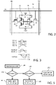
- each memory cell 14 includes two cross-coupled CMOS inverters 22 and 24, each inverter including a series connected p-channel and n-channel MOSFET transistor pair.
- the inputs and outputs of the inverters 22 and 24 are coupled to form a latch circuit having a true data storage node QT and a complement data storage node QC which store complementary logic states of the stored data bit.
- the cell 14 further includes two transfer (passgate) transistors 26 and 28 whose gate terminals are driven by a word line WL
- the source-drain path of transistor 26 is connected between the true data storage node QT and a node associated with a true bit line BLT.
- the source-drain path of transistor 28 is connected between the complement data storage node QC and a node associated with a complement bit line BLC.
- the source terminals of the p-channel transistors 30 and 32 in each inverter 22 and 24 are coupled to receive a high supply voltage (for example, Vdd) at a high supply node, while the source terminals of the n-channel transistors 34 and 36 in each inverter 22 and 24 are coupled to receive a low supply voltage (for example, ground (Gnd) reference) at a low supply node.
- FIG. 2 is specific to the use of 6T-type cells, those skilled in the art recognize that the 8T-type cell is similarly configured and would further include a signal path that is coupled to one of the storage nodes and includes a transfer (passgate) transistor coupled to the read word line RWL and gate driven by the signal on the read word line RWL.
- the word line driver circuit 16 is also typically coupled to receive the high supply voltage (Vdd) at the high supply node and is referenced to the low supply voltage (Gnd) at the low supply node.
- the row controller circuit 18 performs the function of selecting which ones of the word lines WL ⁇ 0> to WL ⁇ N-1> are to be simultaneously accessed (or actuated) in parallel during an in-memory compute operation, and further functions to control application of pulsed signals to the word lines in accordance with the feature data for that in-memory compute operation.
- Figure 1 illustrates, by way of example only, the simultaneous actuation of all N word lines with the pulsed word line signals, it being understood that in-memory compute operations may instead utilize a simultaneous actuation of fewer than all rows of the SRAM array.
- analog signal voltages which develop on a given pair of complementary bit lines BLT and BLC are dependent on the logic state of the bits of the computational weight stored in the memory cells 14 of the corresponding column and the width(s) of the pulsed word line signals for the feature data applied to those memory cells 14.
- the implementation illustrated in Figure 1 shows an example in the form of a pulse width modulation (PWM) for the applied word line signals for the in-memory compute operation.
- PWM pulse width modulation
- PTM period pulse modulation
- the pulsed word line signal format can be further evolved as an encoded pulse train to manage block sparsity of the feature data of the in-memory compute operation. It is accordingly recognized that an arbitrary set of encoding schemes for the applied word line signals can be used when simultaneously driving multiple word lines. Furthermore, in a simpler implementation, it will be understood that all applied word line signals in the simultaneous actuation may instead have a same pulse width.
- Figure 3 is a timing diagram showing simultaneous application of the example pulse width modulated word line signals for the feature data to plural rows of memory cells 14 in the SRAM array 12 for a given in-memory compute operation, and the development over time of the analog signal voltages Va,T and Va,C on one corresponding pair of complementary bit lines BLT and BLC, respectively, in response to the pulse width(s) of those word line signals and the logic state of the bits of the computational weight stored in the memory cells 14.
- the representation of the analog voltage Va levels as shown is just an example. After completion of the computation cycle of the in-memory compute operation, the analog voltage Va levels return to the bit line precharge Vdd level.
- the analog voltage on at least one of the bit lines BLT and BLC may fall from the Vdd voltage to a level where an unwanted data flip occurs with respect to the stored data bit value in one of the memory cells 14 of the column. For example, a logic "1" state stored in the cell 14 of a column may be flipped to a logic "0" state. This data flip introduces a data error in the computational weight stored in the memory cells, thus jeopardizing the accuracy of subsequent in-memory compute operations.
- the unwanted data flip that occurs due to an excess of bit line voltage lowering is mainly an effect of the simultaneous parallel access of the word lines in matrix vector multiplication mode during the in-memory compute operation.
- This problem is different from normal data flip of an SRAM bit cell due to Static-Noise-Margin (SNM) issues which happens in serial bit cell access when the bit line is close to the level of the supply voltage Vdd.
- SNM Static-Noise-Margin
- the normal data flip is instead caused by a ground bounce of the data storage nodes QT or QC.
- a known solution to address the serial bit cell access SNM failure concern is to lower the word line voltage by a small amount and this is generally achieved by a short circuit of the word line driver and the use of a bleeder path.
- parallel access of multiple word lines during an in-memory compute operation instead needs a Radical-WL Lowering/Modulation (RWLM) technique.
- RWLM Radical-WL Lowering/Modulation
- a known solution to address the foregoing problem is to apply a fixed word line voltage lowering (for example, to apply a voltage V WLUD equal to Vdd/2) on all integrated circuit process corners in order to secure the worst integrated circuit process corner.
- This word line underdrive (WLUD) solution has a known drawback in that there is a corresponding reduction in read current on the bit lines which can have a negative impact on computation performance. Furthermore, the use of a fixed word line underdrive voltage can increase variability of the read current across the array leading to accuracy loss for the in-memory compute operation.
- Another solution is to utilize a specialized bitcell circuit design for each memory cell 14 that is less likely to suffer from an unwanted data flip during simultaneous (parallel) access of multiple rows for the in-memory compute operation.
- a concern with this solution is an increase in occupied circuit area for such a bitcell circuit. It would be preferred for some in-memory computation circuit applications to retain the advantages provided by use of the standard 6T SRAM cell ( Figure 2 ) or 8T SRAM cell or topologically similar bit cell in the array 12.
- an in-memory computation circuit comprises: a memory array including a plurality of static random access memory (SRAM) cells arranged in a matrix with plural rows and plural columns, each row including a word line connected to the SRAM cells of the row, and each column including a pair of bit lines connected to the SRAM cells of the column; a word line drive circuit for each row having an output connected to drive the word line of the row, wherein the word line drive circuit is powered by an adaptive supply voltage; a row controller circuit configured to simultaneously actuate the plurality of word lines by applying pulses through the word line driver circuits to the word lines for an in-memory compute operation; a column processing circuit connected to the pair of bit lines for each column and configured to process analog voltages developed on the pairs of bit lines in response to the simultaneous actuation of the plurality of word lines to generate a decision output for the in-memory compute operation; and a voltage generator circuit configured to generate the adaptive supply voltage for powering the word line drive circuits during the simultaneous actuation of the plurality of
- an in-memory computation circuit comprises: a memory array including a plurality of static random access memory (SRAM) cells arranged in a matrix with plural rows and plural columns, each row including a word line connected to the SRAM cells of the row, and each column including a pair of bit lines connected to the SRAM cells of the column; a word line drive circuit for each row having an output connected to drive the word line of the row; a row controller circuit configured to simultaneously actuate the plurality of word lines by applying pulses through the word line driver circuits to word lines for an in-memory compute operation; a column processing circuit connected to the pair of bit lines for each column and configured to process analog voltages developed on the pairs of bit lines in response to the simultaneous actuation of the plurality of word lines to generate a decision output for the in-memory compute operation; a bleeder transistor for each word line, wherein each bleeder transistor has a source-drain path coupled between the word line and a reference voltage node and a gate configured to receive an adaptive bias voltage
- an in-memory computation circuit comprises: a memory array including a plurality of static random access memory (SRAM) cells arranged in a matrix with plural rows and plural columns, each row including a word line connected to the SRAM cells of the row, and each column including a pair of bit lines connected to the SRAM cells of the column; a word line drive circuit for each row having an output connected to drive the word line of the row, wherein the word line drive circuit is powered by an adaptive supply voltage; a row controller circuit configured to simultaneously actuate the plurality of word lines by applying pulses through the word line driver circuits to the word lines for an in-memory compute operation; a column processing circuit connected to the pair of bit lines for each column and configured to process analog voltages developed on the pairs of bit lines in response to the simultaneous actuation of the plurality of word lines to generate a decision output for the in-memory compute operation; a replica circuit that replicates a passgate transistor and pull down transistor of the SRAM cells; a current generator configured to apply a force current
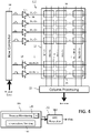
- FIG. 4 shows a schematic diagram of an in-memory computation circuit 110 utilizing an adaptive supply voltage Vbias for word line driving.
- the supply voltage for the word line driver circuit 16 is an adaptive supply voltage Vbias that is modulated dependent on integrated circuit process and/or temperature conditions.
- the voltage level of this adaptive supply voltage Vbias is less than the supply voltage Vdd (used by the memory cells 14, for example) and is generated by a voltage generator circuit 112.
- the voltage generator circuit 112 may comprise a voltage regulator such as a low drop-out (LDO) voltage regulator, which is a circuit well known to those skilled in the art.
- LDO low drop-out
- the voltage generator circuit 112 receives the supply voltage Vdd and a control signal.
- the control signal is a multi-bit digital control signal Vsel, but it will be understood that the control signal can instead be implemented as an analog signal.
- the value of the control signal (in particular, the digital values of the bits of the control signal Vsel) select the voltage level of the adaptive supply voltage Vbias output by the voltage generator circuit 112.
- the control signal Vsel is generated by a control circuit 114 in response to integrated circuit process and/or temperature information, and thus the voltage level of the adaptive supply voltage Vbias is modulated in a manner which is dependent on that integrated circuit process and/or temperature information.
- the integrated circuit process information is a digital code generated and stored in a memory M within the control circuit 114.
- the digital code represents the centering of the process lot and is generated by circuitry such as, for example, ring oscillators (RO) whose output frequency varies dependent on integrated circuit process.
- the output frequencies of the RO circuits thus represent the process centering and can easily be converted into a digital code (for example, through the use of counter circuits).
- a process monitoring circuit 116 within the control circuit 114 can generate the value of the control signal Vsel as a function of the stored digital code for the integrated circuit process.
- the process monitoring circuit 116 may include a look-up table (LUT) that correlates each digital code with a value of the control signal Vsel for providing a specific voltage level of the adaptive supply voltage Vbias that will produce an optimal level of word line underdrive for the integrated circuit process corner.
- the control circuit 114 outputs the value of the control signal Vsel correlated to the stored digital code and the voltage generator circuit 112 responds by generating the corresponding level for the adaptive supply voltage Vbias.
- the temperature information is generated by a temperature sensing circuit 118 and represents a current temperature of the integrated circuit.
- the temperature sensing circuit 118 may select, modify or adjust the value of the control signal Vsel as a function of the sensed temperature.
- the temperature sensing circuit 118 may include a look-up table (LUT) that specifies a certain (positive or negative) adjustment in the value of the control signal Vsel for providing a corresponding tuning of the specific voltage level of the adaptive supply voltage Vbias that will produce the optimal level of word line underdrive given the integrated circuit process corner and current temperature condition.
- LUT look-up table
- step 140 the stored digital code for the integrated circuit process is read from the memory M.
- the digital code for the integrated circuit process is loaded at the factory into the memory M, and this digital code is based on the identified integrated circuit process characteristic (fast/slow corner, etc.) for the integrated circuit fabrication lot (for example, the source wafer) from which the integrated circuit is obtained.
- step 142 a determination is made as to whether the read digital code for the integrated circuit process indicates that the n-channel MOSFET devices of the memory cells 12 are at the fast integrated circuit process corner (e.g., where and NMOS speed is fast and PMOS speed is slow - the "FS" corner). If yes, then a value of the control signal Vsel is selected in step 144 which corresponds to the read digital code and which will cause the voltage generator circuit 112 to generate a higher degree of word line underdrive (i.e., the voltage level for the adaptive supply voltage Vbias will be lower than a nominal (or default) voltage level for word line underdrive).
- the effect of setting the adaptive supply voltage Vbias to a voltage level that is lower than the nominal (or default) voltage level is to reduce the multi row access write margin (MRAWM) which is the maximum level of the bit-line voltage needed to write into bit-cell. Reducing the MRAWM results in degradation of the write-ability of the bit cell and improvement of the data flip rate which are of concern at the fast NMOS corners. It will be understood by those skilled in the art that this is different from the normal Write Margin of the bit cell.
- This lower than nominal (or default) voltage level also enables a higher headroom for bit line swing, and as a result there is a higher precision for the bit line accumulation value in the in-memory compute operation.
- step 146 a determination is made as to whether the read digital code for the integrated circuit process indicates that the n-channel MOSFET devices of the memory cells 12 are at the slow integrated circuit process corner (e.g., where NMOS speed is slow and PMOS speed is fast - the "SF" corner). If yes, then a value of the control signal Vsel is selected in step 148 which corresponds to the read digital code and which will cause the voltage generator circuit 112 to generate a lower degree of word line underdrive (i.e., the voltage level for the adaptive supply voltage Vbias is higher than the nominal (or default) voltage level for word line underdrive).
- step 150 a value of the control signal Vsel is selected which corresponds to the read digital code and which will cause the voltage generator circuit 112 to generate a voltage level for the adaptive supply voltage Vbias that is equal to the nominal (or default) voltage level for word line underdrive.
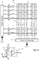
- FIG. 6 shows a schematic diagram of an in-memory computation circuit 210 utilizing an adaptive supply voltage Vbias for word line driving.
- the voltage level of this adaptive supply voltage Vbias is less than the supply voltage Vdd (used by the memory cells 14, for example) and is generated by a voltage generator circuit 212 with a voltage level that is proportional (by a factor of n) to a reference current Iref level.
- the reference current Iref has a magnitude defined by the fast NMOS process lot.
- the reference current Iref for a given bit cell is the current where MRAWM is zero while allowing for full rail-to-rail swing of bit lines at the worst process corner.
- the value of n for the proportionality factor is set by design and is based on a desired variability of the adaptive supply voltage Vbias level (such that n numbers of replica will effectively minimize the variation of Vbias due to local variation).
- the voltage generator circuit 212 includes a current source 214 powered from the supply voltage Vdd and generating an output current lout at node 216 where the current source is connected in series with the series connection of a first n-channel MOSFET device 218 and second n-channel MOSFET device 220.
- the output current lout is applied (i.e., forced) to a circuit with transistors 218 and 220 to generate the bias voltage Vbias, wherein the transistors 218 and 220 effectively replicate the pass-gate and pull-down transistor configuration depicting the read condition of the memory cell.
- the first n-channel MOSFET device 218 has a drain coupled (preferably directly connected) to node 216 and a source coupled (preferably directly connected) to node 222.
- a gate of the first n-channel MOSFET device 218 is coupled (preferably directly connected) to the drain at node 216, thus configuring device 218 as a diode-connected transistor.
- the first n-channel MOSFET device 218 is a scaled replica of the n-channel transfer (passgate) transistors 26 and 28 within each memory cell 14, where the scaling factor is equal to n.
- scaled replica means that the transistor 218 is made identically using the same integrated circuit process materials and parameters (doping levels, oxide thickness, gate materials, etc.) as each of the transistors 26 and 28 but is an n times repetition of the single transistor providing an effectively larger width.
- the transistor 218 may be fabricated by connecting n transistors in parallel which are identical (matching) to each of the transistors 26 and 28.
- the second n-channel MOSFET device 220 has a drain coupled (preferably directly connected) to node 222 and a source coupled (preferably directly connected) to the ground supply reference.
- a gate of the second n-channel MOSFET device 220 is coupled (preferably directly connected) to receive the supply voltage Vdd.
- the second n-channel MOSFET device 220 is a scaled replica of the n-channel pulldown transistors 34 and 36 within each memory cell 14, where the scaling factor is equal to n.
- the transistor 220 may be fabricated by connecting n transistors in parallel which are identical (matching) to each of the transistors 34 and 36.
- the series connected transistors 218 and 220 replicate, subject to the scaling factor n, the current path in the memory cell 14 from the bit line (BLT or BLC) to ground in the operating condition where the pass gate transistor and its pull down transistor on one side of the memory cell are both turned on during the read operation.
- a differential amplifier circuit 224 configured as a unity gain voltage follower receives the Vbias voltage at its non-inverting input and generates the Vbias voltage at its output 226 with sufficient drive capacity to power all of the word line driver circuits 16 for the simultaneously actuated word lines during an in-memory compute operation.
- the output of the differential amplifier circuit 224 is shorted to the inverting input.
- FIG. 7 shows a schematic diagram of an in-memory computation circuit 310 utilizing an adaptive supply voltage Vbias for word line driving.
- the circuit 310 differs from the circuit 210 in that a further integrated circuit process and/or temperature based tuning of the magnitude of the current lout output by the current source 214 within the voltage generator circuit 212 is supported.
- the current source 214 is formed by a variable current source having a base (or nominal) current Inom magnitude equal to n(Iref) with a positive or negative adjustment adj from that base current magnitude level set by a control signal.
- the magnitude of the current output lout by the current source 214 is equal to n(Iref) ⁇ adj, where adj is the adjustment set by the control signal.
- the control signal is a multi-bit digital control signal Vsel, but it will be understood that the control signal can instead be implemented as an analog signal.
- the value of the control signal (in particular, the digital values of the bits of the control signal Vsel) selects the degree of adjustment made to the magnitude of the current output by the current source 214.
- the control signal Vsel is generated by a control circuit 114 in response to integrated circuit process and/or temperature information.
- the level of the adaptive supply voltage Vbias is now additionally dependent on that integrated circuit process and/or temperature information.
- the integrated circuit process information is a digital code generated and stored in a memory M within the control circuit 114.
- the digital code represents the centering of the process lot and is generated by circuitry such as, for example, ring oscillators (RO) whose output frequency varies dependent on integrated circuit process.
- the output frequencies of the RO circuits thus represent the process centering and can easily be converted into a digital code (for example, through the use of counter circuits).
- a process monitoring circuit 116 within the control circuit 114 can generate the value of the control signal Vsel as a function of the stored digital code for the integrated circuit process.
- the process monitoring circuit 116 may include a look-up table (LUT) that correlates each digital code with a value of the control signal Vsel for selecting the positive or negative adjustment adj of the nominal magnitude of the current generated by the current source 214 to ensure that the voltage level of the adaptive supply voltage Vbias will produce the optimal level of word line underdrive for the integrated circuit process corner.
- the control circuit 114 outputs the value of the control signal Vsel correlated to the digital code and the voltage generator circuit 212 responds by generating the corresponding voltage level for the adaptive supply voltage Vbias.
- the temperature information is generated by a temperature sensing circuit 118 and represents a current temperature of the integrated circuit.
- the temperature sensing circuit 118 may modify or adjust the value of the control signal Vsel as a function of the sensed temperature.
- the temperature sensing circuit 118 may include a look-up table (LUT) that specifies a certain adjustment in the value of the control signal Vsel for providing a corresponding tuning of the magnitude of the current output by the current source 214 to ensure that the level of the adaptive supply voltage Vbias will produce the optimal level of word line underdrive given the integrated circuit process corner and current temperature condition.
- LUT look-up table
- step 140 the stored digital code for the integrated circuit process is read from the memory M.
- the digital code for the integrated circuit process is loaded at the factory into the memory M, and this digital code is based on the identified integrated circuit process characteristic (fast/slow corner, etc.) for the integrated circuit fabrication lot (for example, the source wafer) from which the integrated circuit is obtained.
- step 142 a determination is made as to whether the read digital code for the integrated circuit process indicates that the n-channel MOSFET devices of the memory cells 12 are at the fast integrated circuit process corner (i.e., where and NMOS speed is fast and PMOS speed is slow - the "FS" corner).
- a value of the control signal Vsel is selected in step 144 which corresponds to the read digital code and which will cause a negative adjustment adj in the magnitude of the current output by the current source 214 so that the voltage regulator circuit 212 will produce a higher degree of word line underdrive (i.e., the level for the adaptive supply voltage Vbias will be lower than a nominal (or default) level for word line underdrive set by the nominal current magnitude n(Iref)).
- the effect of setting the adaptive supply voltage Vbias to a voltage level that is lower than the nominal (or default) voltage level is to reduce the multi row access write margin (MRAWM) which is the maximum level of the bit-line voltage needed to write into bit-cell.
- MRAWM multi row access write margin
- step 142 a determination is made as to whether the read digital code for the integrated circuit process indicates that the n-channel MOSFET devices of the memory cells 12 are at the slow integrated circuit process corner (i.e., where NMOS speed is slow and PMOS speed is fast - the "SF" corner).
- a value of the control signal Vsel is selected in step 148 which corresponds to the read digital code and which will cause a positive adjustment adj in the magnitude of the current output by the current source 214 so that the voltage regulator circuit 212 will produce a lower degree of word line underdrive (i.e., the level for the adaptive supply voltage Vbias is higher than the nominal (or default) level for word line underdrive set by the nominal current magnitude n(Iref)).
- the effect of setting the adaptive supply voltage Vbias to a voltage level that is higher than the nominal (or default) voltage level is to increase the multi row access write margin (MRAWM), resulting in an improved cell current while still controlling the data flip rate which is of less concern at slow NMOS corners.
- MRAWM multi row access write margin
- FIG. 8 shows a schematic diagram of an in-memory computation circuit 410 utilizing an integrated circuit process and/or temperature dependent word line underdrive.
- the circuit 410 differs from the circuit 10 in the inclusion, for each word line, of a bleeder (n-channel pull down) MOSFET device 412 having a source-drain path coupled between the word line and the ground reference and a gate coupled to receive an adaptive gate bias voltage Vgbias modulated dependent on integrated circuit process and/or temperature conditions to control the applied level of word line underdrive.
- the adaptive gate bias voltage Vgbias is generated by a voltage generator circuit 112.
- the voltage generator circuit 112 may comprise a voltage regulator such as a low drop-out (LDO) voltage regulator, which is a circuit well known to those skilled in the art.
- LDO low drop-out
- the voltage generator circuit 112 receives the supply voltage Vdd and a control signal.
- the control signal is a multi-bit digital control signal Vsel, but it will be understood that the control signal can instead be implemented as an analog signal.
- the value of the control signal (in particular, the digital values of the bits of the control signal Vsel) selects the level of the adaptive gate bias voltage Vgbias output by the voltage generator circuit 112.
- the control signal Vsel is generated by a control circuit 114 in response to integrated circuit process and/or temperature information.
- the level of the adaptive gate bias voltage Vgbias controls the conductivity of the bleeder transistors 412 and thus the applied level of word line underdrive is dependent on that integrated circuit process and/or temperature information.
- the integrated circuit process information is a digital code generated and stored in a memory M within the control circuit 114.
- the digital code represents the centering of the process lot and is generated by circuitry such as, for example, ring oscillators (RO) whose output frequency varies dependent on integrated circuit process.
- the output frequencies of the RO circuits thus represent the process centering and can easily be converted into a digital code (for example, through the use of counter circuits).
- a process monitoring circuit 116 within the control circuit 114 can generate the value of the control signal Vsel as a function of the stored digital code for the integrated circuit process.
- the process monitoring circuit 116 may include a look-up table (LUT) that correlates each digital code with a value of the control signal Vsel for providing a specific voltage level of the adaptive gate bias voltage Vbias that will produce an optimal level of word line underdrive for the integrated circuit process corner.
- the control circuit 114 outputs the value of the control signal Vsel correlated to the digital code and the voltage generator circuit 112 responds by generating the corresponding voltage level for the adaptive gate bias voltage Vgbias.
- the temperature information is generated by a temperature sensing circuit 118 and represents a current temperature of the integrated circuit.
- the temperature sensing circuit 118 may modify or adjust the value of the control signal Vsel as a function of the sensed temperature.
- the temperature sensing circuit 118 may include a look-up table (LUT) that specifies a certain adjustment in the value of the control signal Vsel for providing a corresponding tuning of the specific voltage level of the adaptive gate bias voltage Vgbias that will produce the optimal level of word line underdrive given the integrated circuit process corner and current temperature condition.
- LUT look-up table
- step 140 the stored digital code for the integrated circuit process is read from the memory M.
- the digital code for the integrated circuit process is loaded at the factory into the memory M, and this digital code is based on the identified integrated circuit process characteristic (fast/slow corner, etc.) for the integrated circuit fabrication lot (for example, the source wafer) from which the integrated circuit is obtained.
- step 142 a determination is made as to whether the read digital code for the integrated circuit process indicates that the n-channel MOSFET devices of the memory cells 12 are at the fast integrated circuit process corner (i.e., where and NMOS speed is fast and PMOS speed is slow - the "FS" corner). If yes, then a value of the control signal Vsel is selected in step 144 which corresponds to the read digital code and which will cause the voltage generator circuit 112 to generate a higher degree of word line underdrive (i.e., the level for the adaptive gate bias voltage Vgbias will be higher than a nominal (or default) level for word line underdrive).
- step 146 a determination is made as to whether the read digital code for the integrated circuit process indicates that the n-channel MOSFET devices of the memory cells 12 are at the slow integrated circuit process corner (i.e., where NMOS speed is slow and PMOS speed is fast - the "SF" corner). If yes, then a value of the control signal Vsel is selected in step 148 which corresponds to the read digital code and which will cause the voltage generator circuit 112 to generate a lower degree of word line underdrive (i.e., the level for the adaptive gate bias voltage Vgbias is lower than the nominal (or default) level for word line underdrive).
- step 150 a value of the control signal Vsel is selected which corresponds to the read digital code and which will cause the voltage generator circuit 112 to generate a level for the adaptive supply voltage Vgbias that is equal to the nominal (or default) level for word line underdrive.
- Example 1 An in-memory computation circuit, comprising:
- Example 2 The in-memory computation circuit of example 1, wherein the voltage generator circuit is an adjustable voltage regulator controlled to generate the level of the adaptive supply voltage, and further comprising a control circuit configured to generate a control signal for application to the voltage generator circuit.
- the voltage generator circuit is an adjustable voltage regulator controlled to generate the level of the adaptive supply voltage, and further comprising a control circuit configured to generate a control signal for application to the voltage generator circuit.
- Example 3 The in-memory computation circuit of example 2, wherein the control signal is configured to cause modulation of the level of the adaptive supply voltage away from a nominal level in response to an applicable integrated circuit process corner for transistor devices of the SRAM cells.
- Example 4 The in-memory computation circuit of example 3, wherein the applicable integrated circuit process corner is indicated by a programmed code stored in the control circuit, and wherein the control circuit includes a lookup table (LUT) correlating the programmed code to a value of the control signal.
- LUT lookup table
- Example 5 The in-memory computation circuit of example 4, wherein the control circuit further comprises a temperature sensor, and wherein the control signal is configured to cause a temperature dependent tuning of the level of the adaptive supply voltage set in response to applicable integrated circuit process corner.
- Example 6 The in-memory computation circuit of example 5, wherein the control circuit includes a lookup table (LUT) correlating sensed integrated circuit temperature to a tuning level for the value of the control signal.
- LUT lookup table
- Example 7 The in-memory computation circuit of any of examples 2 to 6, wherein the control circuit further comprises a temperature sensor, and wherein the control signal is configured to cause modulation of the level of the adaptive supply voltage away from a nominal level in response to an integrated circuit temperature sensed by the temperature sensor.
- Example 8 The in-memory computation circuit of example 7, wherein the control circuit includes a lookup table (LUT) correlating sensed integrated circuit temperature to a value of the control signal.
- LUT lookup table
- Example 9 The in-memory computation circuit of any of examples 1 to 8, wherein the voltage generator circuit comprises:
- Example 10 The in-memory computation circuit of example 9, wherein the current generated by the current source has a magnitude set as a function of a reference current representative of current flowing through the passgate transistor and the pull down transistor for an applicable integrated circuit process corner.
- Example 11 The in-memory computation circuit of example 10, wherein the magnitude of the current generated by the current source is scaled by a factor applied to the reference current.
- Example 12 The in-memory computation circuit of example 11, wherein the first transistor is scaled by said factor for the replica of the passgate transistor and wherein the second transistor is scaled by said factor for the replica of the pull down transistor.
- Example 13 The in-memory computation circuit of any of examples 9 to 12, further comprising an amplifier circuit having an input coupled to said first node and an output coupled to power the word line drive circuits.
- Example 14 The in-memory computation circuit of any of examples 9 to 13, wherein the current source is controlled to generate an adjustment to the current, and further comprising a control circuit configured to generate a control signal for application to the current source.
- Example 15 The in-memory computation circuit of example 14, wherein the control signal is configured to cause modulation of a level of the current away from a nominal level in response to an applicable integrated circuit process corner for transistor devices of the SRAM cells.
- Example 16 The in-memory computation circuit of example 15, wherein the applicable integrated circuit process corner is indicated by a programmed code stored in the control circuit, and wherein the control circuit includes a lookup table (LUT) correlating the programmed code to a value of the control signal.
- LUT lookup table
- Example 17 The in-memory computation circuit of example 15 or 16, wherein the control circuit further comprises a temperature sensor, and wherein the control signal is configured to cause a temperature dependent tuning of the level of the current set in response to applicable integrated circuit process corner.
- Example 18 The in-memory computation circuit of example 17, wherein the control circuit includes a lookup table (LUT) correlating sensed integrated circuit temperature to a tuning level for the value of the control signal.
- LUT lookup table
- Example 19 The in-memory computation circuit of any of examples 14 to 18, wherein the control circuit further comprises a temperature sensor, and wherein the control signal is configured to cause modulation of the level of the current away from a nominal level in response to an integrated circuit temperature sensed by the temperature sensor.
- Example 20 The in-memory computation circuit of example 19, wherein the control circuit includes a lookup table (LUT) correlating sensed integrated circuit temperature to a value of the control signal.
- LUT lookup table
- Example 21 An in-memory computation circuit, comprising:
- Example 22 The in-memory computation circuit of example 21, wherein the voltage generator circuit is an adjustable voltage regulator controlled to generate the level of the adaptive gate bias voltage, and further comprising a control circuit configured to generate a control signal for application to the voltage generator circuit.
- the voltage generator circuit is an adjustable voltage regulator controlled to generate the level of the adaptive gate bias voltage, and further comprising a control circuit configured to generate a control signal for application to the voltage generator circuit.
- Example 23 The in-memory computation circuit of example 22, wherein the control signal is configured to cause modulation of the level of the adaptive gate bias voltage away from a nominal level in response to an applicable integrated circuit process corner for transistor devices of the SRAM cells.
- Example 24 The in-memory computation circuit of example 23, wherein the applicable integrated circuit process corner is indicated by a programmed code stored in the control circuit, and wherein the control circuit includes a lookup table (LUT) correlating the programmed code to a value of the control signal.
- LUT lookup table
- Example 25 The in-memory computation circuit of example 23 or 24, wherein the control circuit further comprises a temperature sensor, and wherein the control signal is configured to cause a temperature dependent tuning of the level of the adaptive gate bias voltage set in response to applicable integrated circuit process corner.
- Example 26 The in-memory computation circuit of example 25, wherein the control circuit includes a lookup table (LUT) correlating sensed integrated circuit temperature to a tuning level for the value of the control signal.
- LUT lookup table
- Example 27 The in-memory computation circuit of any of examples 22 to 26, wherein the control circuit further comprises a temperature sensor, and wherein the control signal is configured to cause modulation of the level of the adaptive gate bias voltage away from a nominal level in response to an integrated circuit temperature sensed by the temperature sensor.
- Example 28 The in-memory computation circuit of example 27, wherein the control circuit includes a lookup table (LUT) correlating sensed integrated circuit temperature to a value of the control signal.
- LUT lookup table
- Example 29 An in-memory computation circuit, comprising:
- Example 30 The in-memory computation circuit of example 29, wherein the voltage circuit is a voltage buffer.
- Example 31 The in-memory computation circuit of example 29 or 30, wherein the force current generated by the current source has a magnitude set as a function of a reference current representative of current flowing through the passgate transistor and pull down transistor of the SRAM cells for an applicable integrated circuit process corner.
- Example 32 The in-memory computation circuit of example 31, wherein the magnitude of the current generated by the current source is scaled by a factor applied to the reference current.
- Example 33 The in-memory computation circuit of example 32, wherein the replica circuit is s scaled by said factor.
- Example 34 The in-memory computation circuit of any of examples 29 to 33, wherein the current generator is controlled to generate an adjustment to the force current, and further comprising a control circuit configured to generate a control signal for application to the current generator.
- Example 35 The in-memory computation circuit of example 34, wherein the control signal is configured to cause modulation of a level of the force current away from a nominal level in response to an applicable integrated circuit process corner for transistor devices of the SRAM cells.
- Example 36 The in-memory computation circuit of example 35, wherein the applicable integrated circuit process corner is indicated by a programmed code stored in the control circuit, and wherein the control circuit includes a lookup table (LUT) correlating the programmed code to a value of the control signal.
- LUT lookup table
- Example 37 The in-memory computation circuit of example 35 or 36, wherein the control circuit further comprises a temperature sensor, and wherein the control signal is configured to cause a temperature dependent tuning of the level of the force current set in response to applicable integrated circuit process corner.
- Example 38 The in-memory computation circuit of example 37, wherein the control circuit includes a lookup table (LUT) correlating sensed integrated circuit temperature to a tuning level for the value of the control signal.
- LUT lookup table
- Example 39 The in-memory computation circuit of any of examples 34 to 38, wherein the control circuit further comprises a temperature sensor, and wherein the control signal is configured to cause modulation of the level of the force current away from a nominal level in response to an integrated circuit temperature sensed by the temperature sensor.
- Example 40 The in-memory computation circuit of example 39, wherein the control circuit includes a lookup table (LUT) correlating sensed integrated circuit temperature to a value of the control signal.
- LUT lookup table
Landscapes
- Engineering & Computer Science (AREA)
- Microelectronics & Electronic Packaging (AREA)
- Computer Hardware Design (AREA)
- Physics & Mathematics (AREA)
- Theoretical Computer Science (AREA)
- Computing Systems (AREA)
- General Engineering & Computer Science (AREA)
- Mathematical Physics (AREA)
- General Physics & Mathematics (AREA)
- Power Engineering (AREA)
- Quality & Reliability (AREA)
- Health & Medical Sciences (AREA)
- Life Sciences & Earth Sciences (AREA)
- Biomedical Technology (AREA)
- General Health & Medical Sciences (AREA)
- Molecular Biology (AREA)
- Neurology (AREA)
- Static Random-Access Memory (AREA)
Abstract
Description
- This application claims priority from
United States Applications for Patent No. 63/220,152, filed July 9, 2021 17/844,434, filed June 20, 2022 - Embodiments relate to an in-memory computation circuit utilizing a static random access memory (SRAM) array and, in particular, to exercising adaptive word line underdrive control during a simultaneous access of multiple rows of the SRAM array for an in-memory compute operation.
- Reference is made to
Figure 1 which shows a schematic diagram of an in-memory computation circuit 10. Thecircuit 10 utilizes a static random access memory (SRAM)array 12 formed by standard 6TSRAM memory cells 14 arranged in a matrix format having N rows and M columns. As an alternative, a standard 8T memory cell or an SRAM with a similar functionality and topology could instead be used. Eachmemory cell 14 is programmed to store a bit of a computational weight for an in-memory compute operation. In this context, the in-memory compute operation is understood to be a form of a high dimensional Matrix Vector Multiplication (MVM) supporting multi-bit weights that are stored in multiple bit cells of the memory. The group of bit cells (in the case of a multibit weight) can be considered as a virtual synaptic element. Each bit of the computational weight has either a logic "1" or a logic "0" value. - Each
SRAM cell 14 includes a word line WL and a pair of complementary bit lines BLT and BLC. The 8T-type SRAM cell would additionally include a read word line RWL and a read bit line RBT. Thecells 14 in a common row of the matrix are connected to each other through a common word line WL (and through the common read word line RWL in the 8T-type implementation). Thecells 14 in a common column of the matrix are connected to each other through a common pair of complementary bit lines BLT and BLC (and through the common read bit line RBL in the 8T-type implementation). Each word line WL, RWL is driven by a wordline driver circuit 16 which may be implemented as a CMOS driver circuit (for example, a series connected p-channel and n-channel MOSFET transistor pair forming a logic inverter circuit). The word line signals applied to the word lines, and driven by the wordline driver circuits 16, are generated from feature data input to the in-memory computation circuit 10 and controlled by arow controller circuit 18. Acolumn processing circuit 20 senses the analog signal voltages on the pairs of complementary bit lines BLT and BLC (and/or on the read bit line RBL) for the M columns and generates a decision output for the in-memory compute operation from those analog signal voltages. Thecolumn processing circuit 20 can be implemented to support processing where the voltages on the columns are first processed individually and then followed by a recombination of multiple column outputs. - Although not explicitly shown in
Figure 1 , it will be understood that thecircuit 10 further includes conventional row decode, column decode, and read-write circuits known to those skilled in the art for use in connection with writing bits of the computational weight to, and reading bits of the computational weight from, theSRAM cells 14 of thememory array 12. - With reference now to
Figure 2 , eachmemory cell 14 includes twocross-coupled CMOS inverters inverters cell 14 further includes two transfer (passgate)transistors transistor 26 is connected between the true data storage node QT and a node associated with a true bit line BLT. The source-drain path oftransistor 28 is connected between the complement data storage node QC and a node associated with a complement bit line BLC. The source terminals of the p-channel transistors inverter channel transistors inverter Figure 2 is specific to the use of 6T-type cells, those skilled in the art recognize that the 8T-type cell is similarly configured and would further include a signal path that is coupled to one of the storage nodes and includes a transfer (passgate) transistor coupled to the read word line RWL and gate driven by the signal on the read word line RWL. The wordline driver circuit 16 is also typically coupled to receive the high supply voltage (Vdd) at the high supply node and is referenced to the low supply voltage (Gnd) at the low supply node. - The
row controller circuit 18 performs the function of selecting which ones of the word lines WL<0> to WL<N-1> are to be simultaneously accessed (or actuated) in parallel during an in-memory compute operation, and further functions to control application of pulsed signals to the word lines in accordance with the feature data for that in-memory compute operation.Figure 1 illustrates, by way of example only, the simultaneous actuation of all N word lines with the pulsed word line signals, it being understood that in-memory compute operations may instead utilize a simultaneous actuation of fewer than all rows of the SRAM array. The analog signal voltages which develop on a given pair of complementary bit lines BLT and BLC (or develop on the read bit line RBL in the 8T-type implementation) are dependent on the logic state of the bits of the computational weight stored in thememory cells 14 of the corresponding column and the width(s) of the pulsed word line signals for the feature data applied to thosememory cells 14. - The implementation illustrated in
Figure 1 shows an example in the form of a pulse width modulation (PWM) for the applied word line signals for the in-memory compute operation. The use of PWM or period pulse modulation (PTM) for the applied word line signals is a common technique used for the in-memory compute operation based on the linearity of the vector for the multiply-accumulation (MAC) operation. The pulsed word line signal format can be further evolved as an encoded pulse train to manage block sparsity of the feature data of the in-memory compute operation. It is accordingly recognized that an arbitrary set of encoding schemes for the applied word line signals can be used when simultaneously driving multiple word lines. Furthermore, in a simpler implementation, it will be understood that all applied word line signals in the simultaneous actuation may instead have a same pulse width. -
Figure 3 is a timing diagram showing simultaneous application of the example pulse width modulated word line signals for the feature data to plural rows ofmemory cells 14 in theSRAM array 12 for a given in-memory compute operation, and the development over time of the analog signal voltages Va,T and Va,C on one corresponding pair of complementary bit lines BLT and BLC, respectively, in response to the pulse width(s) of those word line signals and the logic state of the bits of the computational weight stored in thememory cells 14. The representation of the analog voltage Va levels as shown is just an example. After completion of the computation cycle of the in-memory compute operation, the analog voltage Va levels return to the bit line precharge Vdd level. It will be noted that a risk exists that the analog voltage on at least one of the bit lines BLT and BLC may fall from the Vdd voltage to a level where an unwanted data flip occurs with respect to the stored data bit value in one of thememory cells 14 of the column. For example, a logic "1" state stored in thecell 14 of a column may be flipped to a logic "0" state. This data flip introduces a data error in the computational weight stored in the memory cells, thus jeopardizing the accuracy of subsequent in-memory compute operations. - The unwanted data flip that occurs due to an excess of bit line voltage lowering is mainly an effect of the simultaneous parallel access of the word lines in matrix vector multiplication mode during the in-memory compute operation. This problem is different from normal data flip of an SRAM bit cell due to Static-Noise-Margin (SNM) issues which happens in serial bit cell access when the bit line is close to the level of the supply voltage Vdd. During serial access, the normal data flip is instead caused by a ground bounce of the data storage nodes QT or QC.
- A known solution to address the serial bit cell access SNM failure concern is to lower the word line voltage by a small amount and this is generally achieved by a short circuit of the word line driver and the use of a bleeder path. However, parallel access of multiple word lines during an in-memory compute operation instead needs a Radical-WL Lowering/Modulation (RWLM) technique. Additionally, a known solution to address the foregoing problem is to apply a fixed word line voltage lowering (for example, to apply a voltage VWLUD equal to Vdd/2) on all integrated circuit process corners in order to secure the worst integrated circuit process corner. This word line underdrive (WLUD) solution, however, has a known drawback in that there is a corresponding reduction in read current on the bit lines which can have a negative impact on computation performance. Furthermore, the use of a fixed word line underdrive voltage can increase variability of the read current across the array leading to accuracy loss for the in-memory compute operation.
- Another solution is to utilize a specialized bitcell circuit design for each
memory cell 14 that is less likely to suffer from an unwanted data flip during simultaneous (parallel) access of multiple rows for the in-memory compute operation. A concern with this solution is an increase in occupied circuit area for such a bitcell circuit. It would be preferred for some in-memory computation circuit applications to retain the advantages provided by use of the standard 6T SRAM cell (Figure 2 ) or 8T SRAM cell or topologically similar bit cell in thearray 12. - There is accordingly a need in the art to support in-memory computation circuit use of a standard 6T (or 8T) SRAM cell while ensuring against unwanted data flip during simultaneous row access.
- In an embodiment, an in-memory computation circuit comprises: a memory array including a plurality of static random access memory (SRAM) cells arranged in a matrix with plural rows and plural columns, each row including a word line connected to the SRAM cells of the row, and each column including a pair of bit lines connected to the SRAM cells of the column; a word line drive circuit for each row having an output connected to drive the word line of the row, wherein the word line drive circuit is powered by an adaptive supply voltage; a row controller circuit configured to simultaneously actuate the plurality of word lines by applying pulses through the word line driver circuits to the word lines for an in-memory compute operation; a column processing circuit connected to the pair of bit lines for each column and configured to process analog voltages developed on the pairs of bit lines in response to the simultaneous actuation of the plurality of word lines to generate a decision output for the in-memory compute operation; and a voltage generator circuit configured to generate the adaptive supply voltage for powering the word line drive circuits during the simultaneous actuation of the plurality of word lines for the in-memory compute operation, said adaptive supply voltage having a level which is dependent on integrated circuit process and/or temperature conditions.
- In an embodiment, an in-memory computation circuit comprises: a memory array including a plurality of static random access memory (SRAM) cells arranged in a matrix with plural rows and plural columns, each row including a word line connected to the SRAM cells of the row, and each column including a pair of bit lines connected to the SRAM cells of the column; a word line drive circuit for each row having an output connected to drive the word line of the row; a row controller circuit configured to simultaneously actuate the plurality of word lines by applying pulses through the word line driver circuits to word lines for an in-memory compute operation; a column processing circuit connected to the pair of bit lines for each column and configured to process analog voltages developed on the pairs of bit lines in response to the simultaneous actuation of the plurality of word lines to generate a decision output for the in-memory compute operation; a bleeder transistor for each word line, wherein each bleeder transistor has a source-drain path coupled between the word line and a reference voltage node and a gate configured to receive an adaptive bias voltage; and a voltage generator circuit configured to generate the adaptive bias voltage during the simultaneous actuation of the plurality of word lines for the in-memory compute operation, said adaptive bias voltage having a level which is dependent on integrated circuit process and/or temperature conditions.
- In an embodiment, an in-memory computation circuit comprises: a memory array including a plurality of static random access memory (SRAM) cells arranged in a matrix with plural rows and plural columns, each row including a word line connected to the SRAM cells of the row, and each column including a pair of bit lines connected to the SRAM cells of the column; a word line drive circuit for each row having an output connected to drive the word line of the row, wherein the word line drive circuit is powered by an adaptive supply voltage; a row controller circuit configured to simultaneously actuate the plurality of word lines by applying pulses through the word line driver circuits to the word lines for an in-memory compute operation; a column processing circuit connected to the pair of bit lines for each column and configured to process analog voltages developed on the pairs of bit lines in response to the simultaneous actuation of the plurality of word lines to generate a decision output for the in-memory compute operation; a replica circuit that replicates a passgate transistor and pull down transistor of the SRAM cells; a current generator configured to apply a force current to the replica circuit to generate a bias voltage; and a voltage circuit configured to use the bias voltage to generate the adaptive supply voltage for powering the word line drive circuits during the simultaneous actuation of the plurality of word lines for the in-memory compute operation, said adaptive supply voltage having a level which is dependent on integrated circuit process and/or temperature conditions.
- For a better understanding of the embodiments, reference will now be made by way of example only to the accompanying figures in which:
-
Figure 1 is a schematic diagram of an in-memory computation circuit; -
Figure 2 is a circuit diagram of a standard 6T static random access memory (SRAM) cell as used the memory array of the in-memory computation circuit shown inFigure 1 ; -
Figure 3 is a timing diagram illustrating an in-memory compute operation; -
Figure 4 is a schematic diagram of an in-memory computation circuit utilizing an adaptive supply voltage for word line driving; -
Figure 5 is a flow diagram; -
Figure 6 is a schematic diagram of an in-memory computation circuit utilizing an adaptive supply voltage for word line driving; -
Figure 7 is a schematic diagram of an in-memory computation circuit utilizing an adaptive supply voltage for word line driving; and -
Figure 8 is a schematic diagram of an in-memory computation circuit utilizing an adaptive word line underdrive bias voltage. - Reference is now made to
Figure 4 which shows a schematic diagram of an in-memory computation circuit 110 utilizing an adaptive supply voltage Vbias for word line driving. Like references inFigures 1 and4 refer to like or similar components, the description of which will not be repeated (see, description above). Thecircuit 110 differs from thecircuit 10 in that the supply voltage for the wordline driver circuit 16 is not fixed equal to Vdd (i.e., it is not the same as the array supply voltage) or set with a fixed word line under voltage level (for example, VWLUD = Vdd/2). Instead, the supply voltage for the wordline driver circuit 16 is an adaptive supply voltage Vbias that is modulated dependent on integrated circuit process and/or temperature conditions. The voltage level of this adaptive supply voltage Vbias is less than the supply voltage Vdd (used by thememory cells 14, for example) and is generated by avoltage generator circuit 112. In an embodiment, thevoltage generator circuit 112 may comprise a voltage regulator such as a low drop-out (LDO) voltage regulator, which is a circuit well known to those skilled in the art. - The
voltage generator circuit 112 receives the supply voltage Vdd and a control signal. In an embodiment, the control signal is a multi-bit digital control signal Vsel, but it will be understood that the control signal can instead be implemented as an analog signal. The value of the control signal (in particular, the digital values of the bits of the control signal Vsel) select the voltage level of the adaptive supply voltage Vbias output by thevoltage generator circuit 112. The control signal Vsel is generated by acontrol circuit 114 in response to integrated circuit process and/or temperature information, and thus the voltage level of the adaptive supply voltage Vbias is modulated in a manner which is dependent on that integrated circuit process and/or temperature information. - The integrated circuit process information is a digital code generated and stored in a memory M within the
control circuit 114. The digital code represents the centering of the process lot and is generated by circuitry such as, for example, ring oscillators (RO) whose output frequency varies dependent on integrated circuit process. The output frequencies of the RO circuits thus represent the process centering and can easily be converted into a digital code (for example, through the use of counter circuits). Aprocess monitoring circuit 116 within thecontrol circuit 114 can generate the value of the control signal Vsel as a function of the stored digital code for the integrated circuit process. For example, theprocess monitoring circuit 116 may include a look-up table (LUT) that correlates each digital code with a value of the control signal Vsel for providing a specific voltage level of the adaptive supply voltage Vbias that will produce an optimal level of word line underdrive for the integrated circuit process corner. Thecontrol circuit 114 outputs the value of the control signal Vsel correlated to the stored digital code and thevoltage generator circuit 112 responds by generating the corresponding level for the adaptive supply voltage Vbias. - The temperature information is generated by a
temperature sensing circuit 118 and represents a current temperature of the integrated circuit. Thetemperature sensing circuit 118 may select, modify or adjust the value of the control signal Vsel as a function of the sensed temperature. For example, thetemperature sensing circuit 118 may include a look-up table (LUT) that specifies a certain (positive or negative) adjustment in the value of the control signal Vsel for providing a corresponding tuning of the specific voltage level of the adaptive supply voltage Vbias that will produce the optimal level of word line underdrive given the integrated circuit process corner and current temperature condition. - Reference is now made to
Figure 5 which shows a flow diagram for operation of thecontrol circuit 114 andprocess monitoring circuit 116 for the circuit ofFigure 4 . Instep 140, the stored digital code for the integrated circuit process is read from the memory M. In an embodiment, the digital code for the integrated circuit process is loaded at the factory into the memory M, and this digital code is based on the identified integrated circuit process characteristic (fast/slow corner, etc.) for the integrated circuit fabrication lot (for example, the source wafer) from which the integrated circuit is obtained. Next, instep 142, a determination is made as to whether the read digital code for the integrated circuit process indicates that the n-channel MOSFET devices of thememory cells 12 are at the fast integrated circuit process corner (e.g., where and NMOS speed is fast and PMOS speed is slow - the "FS" corner). If yes, then a value of the control signal Vsel is selected instep 144 which corresponds to the read digital code and which will cause thevoltage generator circuit 112 to generate a higher degree of word line underdrive (i.e., the voltage level for the adaptive supply voltage Vbias will be lower than a nominal (or default) voltage level for word line underdrive). The effect of setting the adaptive supply voltage Vbias to a voltage level that is lower than the nominal (or default) voltage level is to reduce the multi row access write margin (MRAWM) which is the maximum level of the bit-line voltage needed to write into bit-cell. Reducing the MRAWM results in degradation of the write-ability of the bit cell and improvement of the data flip rate which are of concern at the fast NMOS corners. It will be understood by those skilled in the art that this is different from the normal Write Margin of the bit cell. This lower than nominal (or default) voltage level also enables a higher headroom for bit line swing, and as a result there is a higher precision for the bit line accumulation value in the in-memory compute operation. If no instep 142, then in step 146 a determination is made as to whether the read digital code for the integrated circuit process indicates that the n-channel MOSFET devices of thememory cells 12 are at the slow integrated circuit process corner (e.g., where NMOS speed is slow and PMOS speed is fast - the "SF" corner). If yes, then a value of the control signal Vsel is selected instep 148 which corresponds to the read digital code and which will cause thevoltage generator circuit 112 to generate a lower degree of word line underdrive (i.e., the voltage level for the adaptive supply voltage Vbias is higher than the nominal (or default) voltage level for word line underdrive). The effect of setting the adaptive supply voltage Vbias to a voltage level that is higher than the nominal (or default) voltage level is to increase the multi row access write margin (MRAWM), resulting in an improved cell current while still controlling the data flip rate which is of less concern at slow NMOS corners. This higher than nominal (or default) voltage level also reduces the local variation effect of the slow process corner. If no instep 146, then in step 150 a value of the control signal Vsel is selected which corresponds to the read digital code and which will cause thevoltage generator circuit 112 to generate a voltage level for the adaptive supply voltage Vbias that is equal to the nominal (or default) voltage level for word line underdrive. - Although the process of
Figure 5 contemplates three levels of voltage control (higher than, lower than, and equal to, nominal), it will be understood that this is by example only. Additional testing steps may be added to the process ofFigure 5 to test for other integrated circuit process corner or process-related conditions (for example, fast-fast (FF) and/or slow-slow (SS) corners), with each test having an associated digital code and value of the control signal Vsel for setting a corresponding voltage level of the adaptive supply voltage Vbias generated by thevoltage generator circuit 112. - Reference is now made to
Figure 6 which shows a schematic diagram of an in-memory computation circuit 210 utilizing an adaptive supply voltage Vbias for word line driving. Like references inFigures 1 and6 refer to like or similar components, the description of which will not be repeated (see, description above). Thecircuit 210 differs from thecircuit 10 in that the supply voltage for the wordline driver circuit 16 is not fixed equal to Vdd (i.e., it is not the same as the array supply voltage) or set with a fixed word line under voltage level (for example, VWLUD = Vdd/2). Instead, the supply voltage for the wordline driver circuit 16 is an adaptive supply voltage Vbias modulated dependent on integrated circuit process conditions. The voltage level of this adaptive supply voltage Vbias is less than the supply voltage Vdd (used by thememory cells 14, for example) and is generated by avoltage generator circuit 212 with a voltage level that is proportional (by a factor of n) to a reference current Iref level. The reference current Iref has a magnitude defined by the fast NMOS process lot. As an example, the reference current Iref for a given bit cell is the current where MRAWM is zero while allowing for full rail-to-rail swing of bit lines at the worst process corner. The value of n for the proportionality factor is set by design and is based on a desired variability of the adaptive supply voltage Vbias level (such that n numbers of replica will effectively minimize the variation of Vbias due to local variation). - The
voltage generator circuit 212 includes acurrent source 214 powered from the supply voltage Vdd and generating an output current lout atnode 216 where the current source is connected in series with the series connection of a first n-channel MOSFET device 218 and second n-channel MOSFET device 220. The output current lout is applied (i.e., forced) to a circuit withtransistors transistors channel MOSFET device 218 has a drain coupled (preferably directly connected) tonode 216 and a source coupled (preferably directly connected) tonode 222. A gate of the first n-channel MOSFET device 218 is coupled (preferably directly connected) to the drain atnode 216, thus configuringdevice 218 as a diode-connected transistor. The first n-channel MOSFET device 218 is a scaled replica of the n-channel transfer (passgate)transistors memory cell 14, where the scaling factor is equal to n. In this context, "scaled replica" means that thetransistor 218 is made identically using the same integrated circuit process materials and parameters (doping levels, oxide thickness, gate materials, etc.) as each of thetransistors transistor 218 may be fabricated by connecting n transistors in parallel which are identical (matching) to each of thetransistors channel MOSFET device 220 has a drain coupled (preferably directly connected) tonode 222 and a source coupled (preferably directly connected) to the ground supply reference. A gate of the second n-channel MOSFET device 220 is coupled (preferably directly connected) to receive the supply voltage Vdd. The second n-channel MOSFET device 220 is a scaled replica of the n-channel pulldown transistors memory cell 14, where the scaling factor is equal to n. As an example, thetransistor 220 may be fabricated by connecting n transistors in parallel which are identical (matching) to each of thetransistors - The bias voltage Vbias generated at
node 216 is equal to:
channel MOSFET device 218, and Rdson220 is the resistance from drain to source of the second n-channel MOSFET device 220 gate biased by supply voltage Vdd. The series connectedtransistors memory cell 14 from the bit line (BLT or BLC) to ground in the operating condition where the pass gate transistor and its pull down transistor on one side of the memory cell are both turned on during the read operation. - A
differential amplifier circuit 224 configured as a unity gain voltage follower receives the Vbias voltage at its non-inverting input and generates the Vbias voltage at itsoutput 226 with sufficient drive capacity to power all of the wordline driver circuits 16 for the simultaneously actuated word lines during an in-memory compute operation. The output of thedifferential amplifier circuit 224 is shorted to the inverting input. - Reference is now made to
Figure 7 which shows a schematic diagram of an in-memory computation circuit 310 utilizing an adaptive supply voltage Vbias for word line driving. Like references inFigures 6 and7 refer to like or similar components, the description of which will not be repeated (see, description above). Thecircuit 310 differs from thecircuit 210 in that a further integrated circuit process and/or temperature based tuning of the magnitude of the current lout output by thecurrent source 214 within thevoltage generator circuit 212 is supported. In this context, thecurrent source 214 is formed by a variable current source having a base (or nominal) current Inom magnitude equal to n(Iref) with a positive or negative adjustment adj from that base current magnitude level set by a control signal. In other words, the magnitude of the current output lout by thecurrent source 214 is equal to n(Iref)±adj, where adj is the adjustment set by the control signal. In an embodiment, the control signal is a multi-bit digital control signal Vsel, but it will be understood that the control signal can instead be implemented as an analog signal. The value of the control signal (in particular, the digital values of the bits of the control signal Vsel) selects the degree of adjustment made to the magnitude of the current output by thecurrent source 214. The control signal Vsel is generated by acontrol circuit 114 in response to integrated circuit process and/or temperature information. Thus, the level of the adaptive supply voltage Vbias is now additionally dependent on that integrated circuit process and/or temperature information. - The integrated circuit process information is a digital code generated and stored in a memory M within the
control circuit 114. The digital code represents the centering of the process lot and is generated by circuitry such as, for example, ring oscillators (RO) whose output frequency varies dependent on integrated circuit process. The output frequencies of the RO circuits thus represent the process centering and can easily be converted into a digital code (for example, through the use of counter circuits). Aprocess monitoring circuit 116 within thecontrol circuit 114 can generate the value of the control signal Vsel as a function of the stored digital code for the integrated circuit process. For example, theprocess monitoring circuit 116 may include a look-up table (LUT) that correlates each digital code with a value of the control signal Vsel for selecting the positive or negative adjustment adj of the nominal magnitude of the current generated by thecurrent source 214 to ensure that the voltage level of the adaptive supply voltage Vbias will produce the optimal level of word line underdrive for the integrated circuit process corner. Thecontrol circuit 114 outputs the value of the control signal Vsel correlated to the digital code and thevoltage generator circuit 212 responds by generating the corresponding voltage level for the adaptive supply voltage Vbias. - The temperature information is generated by a
temperature sensing circuit 118 and represents a current temperature of the integrated circuit. Thetemperature sensing circuit 118 may modify or adjust the value of the control signal Vsel as a function of the sensed temperature. For example, thetemperature sensing circuit 118 may include a look-up table (LUT) that specifies a certain adjustment in the value of the control signal Vsel for providing a corresponding tuning of the magnitude of the current output by thecurrent source 214 to ensure that the level of the adaptive supply voltage Vbias will produce the optimal level of word line underdrive given the integrated circuit process corner and current temperature condition. - Reference is now made to
Figure 5 which shows a flow diagram for operation of thecontrol circuit 114 andprocess monitoring circuit 116 for the circuit ofFigure 7 . Instep 140, the stored digital code for the integrated circuit process is read from the memory M. In an embodiment, the digital code for the integrated circuit process is loaded at the factory into the memory M, and this digital code is based on the identified integrated circuit process characteristic (fast/slow corner, etc.) for the integrated circuit fabrication lot (for example, the source wafer) from which the integrated circuit is obtained. Next, instep 142, a determination is made as to whether the read digital code for the integrated circuit process indicates that the n-channel MOSFET devices of thememory cells 12 are at the fast integrated circuit process corner (i.e., where and NMOS speed is fast and PMOS speed is slow - the "FS" corner). If yes, then a value of the control signal Vsel is selected instep 144 which corresponds to the read digital code and which will cause a negative adjustment adj in the magnitude of the current output by thecurrent source 214 so that thevoltage regulator circuit 212 will produce a higher degree of word line underdrive (i.e., the level for the adaptive supply voltage Vbias will be lower than a nominal (or default) level for word line underdrive set by the nominal current magnitude n(Iref)). The effect of setting the adaptive supply voltage Vbias to a voltage level that is lower than the nominal (or default) voltage level is to reduce the multi row access write margin (MRAWM) which is the maximum level of the bit-line voltage needed to write into bit-cell. Reducing the MRAWM results in degradation of the write-ability of the bit cell and improvement of the data flip rate which are of concern at the fast NMOS corners. This lower than nominal (or default) voltage level also enables a higher headroom for bit line swing, and as a result there is a higher precision for the bit line accumulation value in the in-memory compute operation. If no instep 142, then in step 146 a determination is made as to whether the read digital code for the integrated circuit process indicates that the n-channel MOSFET devices of thememory cells 12 are at the slow integrated circuit process corner (i.e., where NMOS speed is slow and PMOS speed is fast - the "SF" corner). If yes, then a value of the control signal Vsel is selected instep 148 which corresponds to the read digital code and which will cause a positive adjustment adj in the magnitude of the current output by thecurrent source 214 so that thevoltage regulator circuit 212 will produce a lower degree of word line underdrive (i.e., the level for the adaptive supply voltage Vbias is higher than the nominal (or default) level for word line underdrive set by the nominal current magnitude n(Iref)). The effect of setting the adaptive supply voltage Vbias to a voltage level that is higher than the nominal (or default) voltage level is to increase the multi row access write margin (MRAWM), resulting in an improved cell current while still controlling the data flip rate which is of less concern at slow NMOS corners. This higher than nominal (or default) voltage level also reduces the local variation effect of the slow process corner. If no instep 146, then in step 150 a value of the control signal Vsel is selected which corresponds to the read digital code and which will cause no adjustment (i.e., adj=0) in the n(Iref) magnitude of the current output by thecurrent source 214 so that thevoltage regulator circuit 212 will produce a level for the adaptive supply voltage Vbias that is equal to the nominal (or default) level for word line underdrive as set by the nominal current Inom. - Although the process of
Figure 5 contemplates three levels of voltage control (higher than, lower than, and equal to, nominal), it will be understood that this is by example only. Additional testing steps may be added to the process ofFigure 5 to test for other integrated circuit process corner or process-related conditions (for example, fast-fast (FF) and/or slow-slow (SS) corners), with each test having an associated digital code and value of the control signal Vsel for setting a corresponding level of the adjustment for the current output by thecurrent source 214 of thevoltage generator circuit 212. - Reference is now made to
Figure 8 which shows a schematic diagram of an in-memory computation circuit 410 utilizing an integrated circuit process and/or temperature dependent word line underdrive. Like references inFigures 1 and8 refer to like or similar components, the description of which will not be repeated (see, description above). Thecircuit 410 differs from thecircuit 10 in the inclusion, for each word line, of a bleeder (n-channel pull down)MOSFET device 412 having a source-drain path coupled between the word line and the ground reference and a gate coupled to receive an adaptive gate bias voltage Vgbias modulated dependent on integrated circuit process and/or temperature conditions to control the applied level of word line underdrive. The adaptive gate bias voltage Vgbias is generated by avoltage generator circuit 112. In an embodiment, thevoltage generator circuit 112 may comprise a voltage regulator such as a low drop-out (LDO) voltage regulator, which is a circuit well known to those skilled in the art. - The
voltage generator circuit 112 receives the supply voltage Vdd and a control signal. In an embodiment, the control signal is a multi-bit digital control signal Vsel, but it will be understood that the control signal can instead be implemented as an analog signal. The value of the control signal (in particular, the digital values of the bits of the control signal Vsel) selects the level of the adaptive gate bias voltage Vgbias output by thevoltage generator circuit 112. The control signal Vsel is generated by acontrol circuit 114 in response to integrated circuit process and/or temperature information. The level of the adaptive gate bias voltage Vgbias controls the conductivity of thebleeder transistors 412 and thus the applied level of word line underdrive is dependent on that integrated circuit process and/or temperature information. - The integrated circuit process information is a digital code generated and stored in a memory M within the
control circuit 114. The digital code represents the centering of the process lot and is generated by circuitry such as, for example, ring oscillators (RO) whose output frequency varies dependent on integrated circuit process. The output frequencies of the RO circuits thus represent the process centering and can easily be converted into a digital code (for example, through the use of counter circuits). Aprocess monitoring circuit 116 within thecontrol circuit 114 can generate the value of the control signal Vsel as a function of the stored digital code for the integrated circuit process. For example, theprocess monitoring circuit 116 may include a look-up table (LUT) that correlates each digital code with a value of the control signal Vsel for providing a specific voltage level of the adaptive gate bias voltage Vbias that will produce an optimal level of word line underdrive for the integrated circuit process corner. Thecontrol circuit 114 outputs the value of the control signal Vsel correlated to the digital code and thevoltage generator circuit 112 responds by generating the corresponding voltage level for the adaptive gate bias voltage Vgbias. - The temperature information is generated by a
temperature sensing circuit 118 and represents a current temperature of the integrated circuit. Thetemperature sensing circuit 118 may modify or adjust the value of the control signal Vsel as a function of the sensed temperature. For example, thetemperature sensing circuit 118 may include a look-up table (LUT) that specifies a certain adjustment in the value of the control signal Vsel for providing a corresponding tuning of the specific voltage level of the adaptive gate bias voltage Vgbias that will produce the optimal level of word line underdrive given the integrated circuit process corner and current temperature condition. - Reference is now made to
Figure 5 which shows a flow diagram for operation of thecontrol circuit 114 andprocess monitoring circuit 116 for the circuit ofFigure 8 . Instep 140, the stored digital code for the integrated circuit process is read from the memory M. In an embodiment, the digital code for the integrated circuit process is loaded at the factory into the memory M, and this digital code is based on the identified integrated circuit process characteristic (fast/slow corner, etc.) for the integrated circuit fabrication lot (for example, the source wafer) from which the integrated circuit is obtained. Next, instep 142, a determination is made as to whether the read digital code for the integrated circuit process indicates that the n-channel MOSFET devices of thememory cells 12 are at the fast integrated circuit process corner (i.e., where and NMOS speed is fast and PMOS speed is slow - the "FS" corner). If yes, then a value of the control signal Vsel is selected instep 144 which corresponds to the read digital code and which will cause thevoltage generator circuit 112 to generate a higher degree of word line underdrive (i.e., the level for the adaptive gate bias voltage Vgbias will be higher than a nominal (or default) level for word line underdrive). If no instep 142, then in step 146 a determination is made as to whether the read digital code for the integrated circuit process indicates that the n-channel MOSFET devices of thememory cells 12 are at the slow integrated circuit process corner (i.e., where NMOS speed is slow and PMOS speed is fast - the "SF" corner). If yes, then a value of the control signal Vsel is selected instep 148 which corresponds to the read digital code and which will cause thevoltage generator circuit 112 to generate a lower degree of word line underdrive (i.e., the level for the adaptive gate bias voltage Vgbias is lower than the nominal (or default) level for word line underdrive). If no instep 146, then in step 150 a value of the control signal Vsel is selected which corresponds to the read digital code and which will cause thevoltage generator circuit 112 to generate a level for the adaptive supply voltage Vgbias that is equal to the nominal (or default) level for word line underdrive. - Although the process of
Figure 5 contemplates three levels of voltage control (higher than, lower than, and equal to, nominal), it will be understood that this is by example only. Additional testing steps may be added to the process ofFigure 5 to test for other integrated circuit process corner or process-related conditions (for example, fast-fast (FF) and/or slow-slow (SS) corners), with each test having an associated digital code and value of the control signal Vsel for setting a corresponding level of the adaptive gate bias voltage Vgbias generated by thevoltage generator circuit 112. - Example embodiments of the invention are summarized here. Other embodiments can also be understood from the entirety of the specification as well as the claims filed herein.
- Example 1. An in-memory computation circuit, comprising:
- a memory array including a plurality of static random access memory (SRAM) cells arranged in a matrix with plural rows and plural columns, each row including a word line connected to the SRAM cells of the row, and each column including at least one bit line connected to the SRAM cells of the column;
- a word line drive circuit for each row having an output connected to drive the word line of the row, wherein the word line drive circuit is powered by an adaptive supply voltage;
- a row controller circuit configured to simultaneously actuate the plurality of word lines by applying pulses through the word line driver circuits to the word lines for an in-memory compute operation;
- a column processing circuit connected to the at least one bit line for each column and configured to process analog voltages developed on the bit lines in response to the simultaneous actuation of the plurality of word lines to generate a decision output for the in-memory compute operation; and
- a voltage generator circuit configured to generate the adaptive supply voltage for powering the word line drive circuits during the simultaneous actuation of the plurality of word lines for the in-memory compute operation, said adaptive supply voltage having a level which is dependent on integrated circuit process and/or temperature conditions.
- Example 2. The in-memory computation circuit of example 1, wherein the voltage generator circuit is an adjustable voltage regulator controlled to generate the level of the adaptive supply voltage, and further comprising a control circuit configured to generate a control signal for application to the voltage generator circuit.
- Example 3. The in-memory computation circuit of example 2, wherein the control signal is configured to cause modulation of the level of the adaptive supply voltage away from a nominal level in response to an applicable integrated circuit process corner for transistor devices of the SRAM cells.
- Example 4. The in-memory computation circuit of example 3, wherein the applicable integrated circuit process corner is indicated by a programmed code stored in the control circuit, and wherein the control circuit includes a lookup table (LUT) correlating the programmed code to a value of the control signal.
- Example 5. The in-memory computation circuit of example 4, wherein the control circuit further comprises a temperature sensor, and wherein the control signal is configured to cause a temperature dependent tuning of the level of the adaptive supply voltage set in response to applicable integrated circuit process corner.
- Example 6. The in-memory computation circuit of example 5, wherein the control circuit includes a lookup table (LUT) correlating sensed integrated circuit temperature to a tuning level for the value of the control signal.
- Example 7. The in-memory computation circuit of any of examples 2 to 6, wherein the control circuit further comprises a temperature sensor, and wherein the control signal is configured to cause modulation of the level of the adaptive supply voltage away from a nominal level in response to an integrated circuit temperature sensed by the temperature sensor.
- Example 8. The in-memory computation circuit of example 7, wherein the control circuit includes a lookup table (LUT) correlating sensed integrated circuit temperature to a value of the control signal.
- Example 9. The in-memory computation circuit of any of examples 1 to 8, wherein the voltage generator circuit comprises:
- a current source configured to generate a current applied to a first node; and
- a series connection of a first and second transistor between the first node and a reference node;
- wherein the adaptive supply voltage is generated at said first node;
- wherein the first transistor is a replica of a passgate transistor within the SRAM cell;
- wherein the second transistor is a replica of a pull down transistor within the SRAM cell.
- Example 10. The in-memory computation circuit of example 9, wherein the current generated by the current source has a magnitude set as a function of a reference current representative of current flowing through the passgate transistor and the pull down transistor for an applicable integrated circuit process corner.
- Example 11. The in-memory computation circuit of example 10, wherein the magnitude of the current generated by the current source is scaled by a factor applied to the reference current.
- Example 12. The in-memory computation circuit of example 11, wherein the first transistor is scaled by said factor for the replica of the passgate transistor and wherein the second transistor is scaled by said factor for the replica of the pull down transistor.
- Example 13. The in-memory computation circuit of any of examples 9 to 12, further comprising an amplifier circuit having an input coupled to said first node and an output coupled to power the word line drive circuits.
- Example 14. The in-memory computation circuit of any of examples 9 to 13, wherein the current source is controlled to generate an adjustment to the current, and further comprising a control circuit configured to generate a control signal for application to the current source.
- Example 15. The in-memory computation circuit of example 14, wherein the control signal is configured to cause modulation of a level of the current away from a nominal level in response to an applicable integrated circuit process corner for transistor devices of the SRAM cells.
- Example 16. The in-memory computation circuit of example 15, wherein the applicable integrated circuit process corner is indicated by a programmed code stored in the control circuit, and wherein the control circuit includes a lookup table (LUT) correlating the programmed code to a value of the control signal.
- Example 17. The in-memory computation circuit of example 15 or 16, wherein the control circuit further comprises a temperature sensor, and wherein the control signal is configured to cause a temperature dependent tuning of the level of the current set in response to applicable integrated circuit process corner.
- Example 18. The in-memory computation circuit of example 17, wherein the control circuit includes a lookup table (LUT) correlating sensed integrated circuit temperature to a tuning level for the value of the control signal.
- Example 19. The in-memory computation circuit of any of examples 14 to 18, wherein the control circuit further comprises a temperature sensor, and wherein the control signal is configured to cause modulation of the level of the current away from a nominal level in response to an integrated circuit temperature sensed by the temperature sensor.
- Example 20. The in-memory computation circuit of example 19, wherein the control circuit includes a lookup table (LUT) correlating sensed integrated circuit temperature to a value of the control signal.
- Example 21. An in-memory computation circuit, comprising:
- a memory array including a plurality of static random access memory (SRAM) cells arranged in a matrix with plural rows and plural columns, each row including a word line connected to the SRAM cells of the row, and each column including at least one bit line connected to the SRAM cells of the column;
- a word line drive circuit for each row having an output connected to drive the word line of the row;
- a row controller circuit configured to simultaneously actuate the plurality of word lines by applying pulses through the word line driver circuits to word lines for an in-memory compute operation;
- a column processing circuit connected to the at least one bit line for each column and configured to process analog voltages developed on the bit lines in response to the simultaneous actuation of the plurality of word lines to generate a decision output for the in-memory compute operation;
- a bleeder transistor for each word line, wherein each bleeder transistor has a source-drain path coupled between the word line and a reference voltage node and a gate configured to receive an adaptive gate bias voltage; and
- a voltage generator circuit configured to generate the adaptive gate bias voltage during the simultaneous actuation of the plurality of word lines for the in-memory compute operation, said adaptive gate bias voltage having a level which is dependent on integrated circuit process and/or temperature conditions.
- Example 22. The in-memory computation circuit of example 21, wherein the voltage generator circuit is an adjustable voltage regulator controlled to generate the level of the adaptive gate bias voltage, and further comprising a control circuit configured to generate a control signal for application to the voltage generator circuit.
- Example 23. The in-memory computation circuit of example 22, wherein the control signal is configured to cause modulation of the level of the adaptive gate bias voltage away from a nominal level in response to an applicable integrated circuit process corner for transistor devices of the SRAM cells.
- Example 24. The in-memory computation circuit of example 23, wherein the applicable integrated circuit process corner is indicated by a programmed code stored in the control circuit, and wherein the control circuit includes a lookup table (LUT) correlating the programmed code to a value of the control signal.
- Example 25. The in-memory computation circuit of example 23 or 24, wherein the control circuit further comprises a temperature sensor, and wherein the control signal is configured to cause a temperature dependent tuning of the level of the adaptive gate bias voltage set in response to applicable integrated circuit process corner.
- Example 26. The in-memory computation circuit of example 25, wherein the control circuit includes a lookup table (LUT) correlating sensed integrated circuit temperature to a tuning level for the value of the control signal.
- Example 27. The in-memory computation circuit of any of examples 22 to 26, wherein the control circuit further comprises a temperature sensor, and wherein the control signal is configured to cause modulation of the level of the adaptive gate bias voltage away from a nominal level in response to an integrated circuit temperature sensed by the temperature sensor.
- Example 28. The in-memory computation circuit of example 27, wherein the control circuit includes a lookup table (LUT) correlating sensed integrated circuit temperature to a value of the control signal.
- Example 29. An in-memory computation circuit, comprising:
- a memory array including a plurality of static random access memory (SRAM) cells arranged in a matrix with plural rows and plural columns, each row including a word line connected to the SRAM cells of the row, and each column including at least one bit line connected to the SRAM cells of the column;
- a word line drive circuit for each row having an output connected to drive the word line of the row, wherein the word line drive circuit is powered by an adaptive supply voltage;
- a row controller circuit configured to simultaneously actuate the plurality of word lines by applying pulses through the word line driver circuits to the word lines for an in-memory compute operation;
- a column processing circuit connected to the at least one bit line for each column and configured to process analog voltages developed on the bit lines in response to the simultaneous actuation of the plurality of word lines to generate a decision output for the in-memory compute operation;
- a replica circuit that replicates a passgate transistor and pull down transistor of the SRAM cells;
- a current generator configured to apply a force current to the replica circuit to generate a bias voltage; and
- a voltage circuit configured to use the bias voltage to generate the adaptive supply voltage for powering the word line drive circuits during the simultaneous actuation of the plurality of word lines for the in-memory compute operation, said adaptive supply voltage having a level which is dependent on integrated circuit process and/or temperature conditions.
- Example 30. The in-memory computation circuit of example 29, wherein the voltage circuit is a voltage buffer.
- Example 31. The in-memory computation circuit of example 29 or 30, wherein the force current generated by the current source has a magnitude set as a function of a reference current representative of current flowing through the passgate transistor and pull down transistor of the SRAM cells for an applicable integrated circuit process corner.
- Example 32. The in-memory computation circuit of example 31, wherein the magnitude of the current generated by the current source is scaled by a factor applied to the reference current.
- Example 33. The in-memory computation circuit of example 32, wherein the replica circuit is s scaled by said factor.
- Example 34. The in-memory computation circuit of any of examples 29 to 33, wherein the current generator is controlled to generate an adjustment to the force current, and further comprising a control circuit configured to generate a control signal for application to the current generator.
- Example 35. The in-memory computation circuit of example 34, wherein the control signal is configured to cause modulation of a level of the force current away from a nominal level in response to an applicable integrated circuit process corner for transistor devices of the SRAM cells.
- Example 36. The in-memory computation circuit of example 35, wherein the applicable integrated circuit process corner is indicated by a programmed code stored in the control circuit, and wherein the control circuit includes a lookup table (LUT) correlating the programmed code to a value of the control signal.
- Example 37. The in-memory computation circuit of example 35 or 36, wherein the control circuit further comprises a temperature sensor, and wherein the control signal is configured to cause a temperature dependent tuning of the level of the force current set in response to applicable integrated circuit process corner.
- Example 38. The in-memory computation circuit of example 37, wherein the control circuit includes a lookup table (LUT) correlating sensed integrated circuit temperature to a tuning level for the value of the control signal.
- Example 39. The in-memory computation circuit of any of examples 34 to 38, wherein the control circuit further comprises a temperature sensor, and wherein the control signal is configured to cause modulation of the level of the force current away from a nominal level in response to an integrated circuit temperature sensed by the temperature sensor.
- Example 40. The in-memory computation circuit of example 39, wherein the control circuit includes a lookup table (LUT) correlating sensed integrated circuit temperature to a value of the control signal.
- The foregoing description has provided by way of exemplary and non-limiting examples a full and informative description of the exemplary embodiment of this invention. However, various modifications and adaptations may become apparent to those skilled in the relevant arts in view of the foregoing description, when read in conjunction with the accompanying drawings and the appended claims. However, all such and similar modifications of the teachings of this invention will still fall within the scope of this invention as defined in the appended claims.
Claims (18)
- An in-memory computation circuit, comprising:a memory array including a plurality of static random access memory (SRAM) cells arranged in a matrix with plural rows and plural columns, each row including a word line connected to the SRAM cells of the row, and each column including at least one bit line connected to the SRAM cells of the column;a word line drive circuit for each row having an output connected to drive the word line of the row;a row controller circuit configured to simultaneously actuate the plurality of word lines by applying pulses through the word line driver circuits to the word lines for an in-memory compute operation;a column processing circuit connected to the at least one bit lines for each column and configured to process analog voltages developed on the bit lines in response to the simultaneous actuation of the plurality of word lines to generate a decision output for the in-memory compute operation; anda voltage generator circuit configured to generate a first voltage during the simultaneous actuation of the plurality of word lines for the in-memory compute operation, said first voltage having a level which is dependent on integrated circuit process and/or temperature conditions.
- The in-memory of claim 1, wherein:
said first voltage is an adaptative supply voltage for powering the word line drive circuits during said simultaneous actuation of the plurality of word lines for the in-memory compute operation. - The in-memory of claim 1, further comprising:
a bleeder transistor for each word line, wherein each bleeder transistor has a source-drain path coupled between the word line and a reference voltage node and a gate configured to receive an adaptive gate bias voltage, said adaptative gate bias voltage being said first voltage generated by said voltage generator circuit during said simultaneous actuation of the plurality of word lines for the in-memory compute operation. - The in-memory computation circuit of any of claims 1 to 3, wherein the voltage generator circuit is an adjustable voltage regulator.
- The in-memory circuit of claim 1, further comprising:a replica circuit that replicates a passgate transistor and pull down transistor of the SRAM cells; anda current generator configured to apply a force current to the replica circuit to generate a bias voltage to be used by said voltage circuit generator to generate said first voltage, said first voltage; said first voltage being an adaptative supply voltage for powering said word line drive circuits during said simultaneous actuation of the plurality of word lines for the in-memory compute operation.
- The in-memory computation circuit of claim 5, wherein the voltage circuit is a voltage buffer.
- The in-memory computation circuit of claim 1 or 2, wherein the voltage generator circuit comprises:a current source configured to generate a current applied to a first node; anda replica circuit comprising a series connection of a first and second transistor between the first node and a reference node;wherein the adaptive supply voltage is generated at said first node;wherein the first transistor is a replica of a passgate transistor within the SRAM cell;wherein the second transistor is a replica of a pull down transistor within the SRAM cell.
- The in-memory computation circuit of claim 7, further comprising an amplifier circuit having an input coupled to said first node and an output coupled to power the word line drive circuits.
- The in-memory computation circuit of any of claims 5 to 8, wherein the current generated by the current generator or source has a magnitude set as a function of a reference current representative of current flowing through the passgate transistor and the pull down transistor for an applicable integrated circuit process corner.
- The in-memory computation circuit of claim 9, wherein the magnitude of the current generated by the current generator or source is scaled by a factor applied to the reference current.
- The in-memory computation circuit of claim 10, wherein the replica circuit is scaled by said factor.
- The in-memory computation circuit of any of claims 5 to 11, wherein the current generator or source is controlled to generate an adjustment to the current, and further comprising a control circuit configured to generate a control signal for application to the current generator or source.
- The in-memory computation circuit of any of claims 1 to 4, wherein the voltage generator circuit is controlled to generate the level of the adaptive supply voltage, or gate bias voltage, and further comprising a control circuit configured to generate a control signal for application to the voltage generator circuit.
- The in-memory computation circuit of claim 12 or 13, wherein the control signal is configured to cause modulation of the level of the adaptive supply voltage, or adaptative gate bias voltage, or current, away from a nominal level in response to an applicable integrated circuit process corner for transistor devices of the SRAM cells.
- The in-memory computation circuit of claim 14, wherein the applicable integrated circuit process corner is indicated by a programmed code stored in the control circuit, and wherein the control circuit includes a lookup table (LUT) correlating the programmed code to a value of the control signal.
- The in-memory computation circuit of claim 14 or 15, wherein the control circuit further comprises a temperature sensor, and wherein the control signal is configured to cause a temperature dependent tuning of the level of the adaptive supply voltage, or adaptative bias voltage, or current, set in response to applicable integrated circuit process corner.
- The in-memory computation circuit of any of claims 12 to 16, wherein the control circuit further comprises a temperature sensor, and wherein the control signal is configured to cause modulation of the level of the adaptive supply voltage, or adaptative bias gate voltage, or current, away from a nominal level in response to an integrated circuit temperature sensed by the temperature sensor.
- The in-memory computation circuit of claim 16 or 17, wherein the control circuit includes a lookup table (LUT) correlating sensed integrated circuit temperature to a tuning level for the value of the control signal, or to a value of the control signal.
Applications Claiming Priority (2)
| Application Number | Priority Date | Filing Date | Title |
|---|---|---|---|
| US202163220152P | 2021-07-09 | 2021-07-09 | |
| US17/844,434 US12354644B2 (en) | 2021-07-09 | 2022-06-20 | Adaptive word line underdrive control for an in-memory compute operation where simultaneous access is made to plural rows of a static random access memory (SRAM) |
Publications (3)
| Publication Number | Publication Date |
|---|---|
| EP4116975A1 true EP4116975A1 (en) | 2023-01-11 |
| EP4116975C0 EP4116975C0 (en) | 2024-08-28 |
| EP4116975B1 EP4116975B1 (en) | 2024-08-28 |
Family
ID=82492547
Family Applications (1)
| Application Number | Title | Priority Date | Filing Date |
|---|---|---|---|
| EP22182469.1A Active EP4116975B1 (en) | 2021-07-09 | 2022-07-01 | Adaptive word line underdrive control for an in-memory compute operation where simultaneous access is made to plural rows of a static random access memory (sram) |
Country Status (3)
| Country | Link |
|---|---|
| US (2) | US12354644B2 (en) |
| EP (1) | EP4116975B1 (en) |
| CN (1) | CN115602227A (en) |
Family Cites Families (77)
| Publication number | Priority date | Publication date | Assignee | Title |
|---|---|---|---|---|
| US5058067A (en) | 1990-06-06 | 1991-10-15 | National Semiconductor Corporation | Individual bit line recovery circuits |
| JP3727191B2 (en) | 1999-02-18 | 2005-12-14 | 松下電器産業株式会社 | Semiconductor memory device |
| EP1155412A1 (en) | 1999-02-22 | 2001-11-21 | Rose Research, L.L.C. | Self-calibrating self-regenerative comparator circuit and method |
| US6282137B1 (en) | 1999-09-14 | 2001-08-28 | Agere Systems Guardian Corp. | SRAM method and apparatus |
| US6529400B1 (en) | 2000-12-15 | 2003-03-04 | Lsi Logic Corporation | Source pulsed, dynamic threshold complementary metal oxide semiconductor static RAM cells |
| US6628540B2 (en) * | 2000-12-31 | 2003-09-30 | Texas Instruments Incorporated | Bias cell for four transistor (4T) SRAM operation |
| US6785161B2 (en) | 2002-06-28 | 2004-08-31 | Micron Technology, Inc. | High voltage regulator for low voltage integrated circuit processes |
| KR20060040614A (en) | 2003-07-01 | 2006-05-10 | 제트모스 테크놀로지 인코포레이티드 | Static Random Access Memory Cell Structures and Circuits |
| US7173837B1 (en) | 2003-09-26 | 2007-02-06 | Netlogic Microsystems, Inc. | Content addressable memory (CAM) cell bit line architecture |
| US7020041B2 (en) | 2003-12-18 | 2006-03-28 | Intel Corporation | Method and apparatus to clamp SRAM supply voltage |
| US7227769B2 (en) | 2004-03-08 | 2007-06-05 | Fujitsu Limited | Semiconductor memory |
| FR2871281B1 (en) | 2004-04-01 | 2008-06-13 | Atmel Corp | METHOD AND DEVICE FOR FEEDING DUAL POWER FOR A NON-VOLATILE MEMORY ON BOARD |
| US20060044018A1 (en) | 2004-04-02 | 2006-03-02 | Chang Augustine W | Variable threshold transistor for the Schottky FPGA and multilevel storage cell flash arrays |
| US7570527B2 (en) | 2005-06-02 | 2009-08-04 | Texas Instruments Incorporated | Static random-access memory having reduced bit line precharge voltage and method of operating the same |
| US7289354B2 (en) | 2005-07-28 | 2007-10-30 | Texas Instruments Incorporated | Memory array with a delayed wordline boost |
| US7400523B2 (en) | 2006-06-01 | 2008-07-15 | Texas Instruments Incorporated | 8T SRAM cell with higher voltage on the read WL |
| US7292495B1 (en) * | 2006-06-29 | 2007-11-06 | Freescale Semiconductor, Inc. | Integrated circuit having a memory with low voltage read/write operation |
| JP5158624B2 (en) * | 2006-08-10 | 2013-03-06 | ルネサスエレクトロニクス株式会社 | Semiconductor memory device |
| JP5057430B2 (en) | 2006-12-18 | 2012-10-24 | ルネサスエレクトロニクス株式会社 | Semiconductor integrated circuit and manufacturing method thereof |
| US7508697B1 (en) * | 2007-05-09 | 2009-03-24 | Purdue Research Foundation | Self-repairing technique in nano-scale SRAM to reduce parametric failures |
| KR101071212B1 (en) | 2007-05-18 | 2011-10-10 | 후지쯔 세미컨덕터 가부시키가이샤 | Semiconductor memory |
| US20090046519A1 (en) | 2007-08-15 | 2009-02-19 | Texas Instruments Incorporated | Method, device and system for configuring a static random access memory cell for improved performance |
| US7564725B2 (en) | 2007-08-31 | 2009-07-21 | Texas Instruments Incorporated | SRAM bias for read and write |
| US7813163B2 (en) | 2007-09-05 | 2010-10-12 | International Business Machines Corporation | Single-ended read and differential write scheme |
| US7760575B2 (en) | 2007-12-31 | 2010-07-20 | Virage Logic Corp. | Memory leakage control circuit and method |
| US7773407B2 (en) | 2008-06-26 | 2010-08-10 | Taiwan Semiconductor Manufacturing Co., Ltd. | 8T low leakage SRAM cell |
| US8134874B2 (en) | 2009-01-16 | 2012-03-13 | Apple Inc. | Dynamic leakage control for memory arrays |
| US8004907B2 (en) | 2009-06-05 | 2011-08-23 | Freescale Semiconductor, Inc. | SRAM with read and write assist |
| US8441829B2 (en) * | 2009-06-12 | 2013-05-14 | Taiwan Semiconductor Manufacturing Company, Ltd. | Stable SRAM cell |
| US8116165B2 (en) | 2010-04-21 | 2012-02-14 | Arm Limited | Memory with improved data reliability |
| US8966329B2 (en) | 2010-07-19 | 2015-02-24 | Arizona Board Of Regents For And On Behalf Of Arizona State University | Fast parallel test of SRAM arrays |
| US8213257B2 (en) | 2010-08-09 | 2012-07-03 | Faraday Technology Corp. | Variation-tolerant word-line under-drive scheme for random access memory |
| US8451652B2 (en) | 2010-12-02 | 2013-05-28 | Lsi Corporation | Write assist static random access memory cell |
| US8559248B2 (en) | 2011-06-14 | 2013-10-15 | Nvidia Corporation | Clamped bit line read circuit |
| US8451679B1 (en) | 2011-08-17 | 2013-05-28 | Lattice Semiconductor Corporation | Dual-port SRAM with bit line clamping |
| US9013949B2 (en) | 2011-12-19 | 2015-04-21 | Advanced Micro Devices, Inc. | Memory access control system and method |
| US8947970B2 (en) | 2012-07-13 | 2015-02-03 | Freescale Semiconductor, Inc. | Word line driver circuits and methods for SRAM bit cell with reduced bit line pre-charge voltage |
| KR101986356B1 (en) | 2012-10-05 | 2019-06-05 | 삼성전자주식회사 | Semiconductor memory device and devices having the same |
| CN105190760B (en) | 2012-11-12 | 2018-04-24 | 马维尔国际贸易有限公司 | Concurrently using the sram cell for passing through both doors by door and PMOS with NMOS in accumulator system |
| KR102083496B1 (en) | 2012-11-21 | 2020-03-02 | 삼성전자 주식회사 | Semiconductor Memory Device for applying temperature-compensated word line voltage in read operation and method thereof |
| US8902672B2 (en) | 2013-01-01 | 2014-12-02 | Memoir Systems, Inc. | Methods and apparatus for designing and constructing multi-port memory circuits |
| US9460776B2 (en) | 2013-01-23 | 2016-10-04 | Nvidia Corporation | SRAM voltage assist |
| US9147451B2 (en) | 2013-03-20 | 2015-09-29 | Arm Limited | Memory device and method of controlling leakage current within such a memory device |
| WO2014185923A1 (en) | 2013-05-16 | 2014-11-20 | Intel Corporation | Low power transient voltage collapse apparatus and method for a memory cell |
| US9953986B2 (en) | 2013-12-20 | 2018-04-24 | Intel Corporation | Method and apparatus for improving read margin for an SRAM bit-cell |
| US9245595B2 (en) | 2013-12-20 | 2016-01-26 | Nvidia Corporation | System and method for performing SRAM access assists using VSS boost |
| US9286952B2 (en) | 2014-06-30 | 2016-03-15 | Lattice Semiconductor Corporation | SRAM with two-level voltage regulator |
| US9697877B2 (en) | 2015-02-05 | 2017-07-04 | The Board Of Trustees Of The University Of Illinois | Compute memory |
| US9336865B1 (en) | 2015-06-02 | 2016-05-10 | M31 Technology Corporation | Multi-port SRAM module and control method thereof |
| US9831852B2 (en) | 2015-08-31 | 2017-11-28 | Texas Instruments Incorporated | Methods and apparatus for a configurable high-side NMOS gate control with improved gate to source voltage regulation |
| US9455023B1 (en) | 2015-10-14 | 2016-09-27 | Oracle International Corporation | Wordline under-driving using a virtual power network |
| US9928898B2 (en) | 2016-03-30 | 2018-03-27 | Qualcomm Incorporated | Wordline adjustment scheme |
| US9799393B1 (en) | 2016-05-31 | 2017-10-24 | Globalfoundries Inc. | Methods, apparatus and system for providing NMOS-only memory cells |
| US9953699B2 (en) | 2016-07-07 | 2018-04-24 | Globalfoundries Inc. | Static random access memory (SRAM) assist circuit |
| US9997236B1 (en) * | 2016-12-12 | 2018-06-12 | Stmicroelectronics International N.V. | Read assist circuit with process, voltage and temperature tracking for a static random access memory (SRAM) |
| KR101935664B1 (en) | 2017-04-26 | 2019-04-03 | 연세대학교 산학협력단 | Differential static random access memory cell |
| US10559573B2 (en) | 2017-09-22 | 2020-02-11 | United Microelectronics Corp. | Static random access memory structure |
| US10403629B2 (en) | 2017-11-06 | 2019-09-03 | Globalfoundries Inc. | Six-transistor (6T) SRAM cell structure |
| US10748911B2 (en) | 2017-11-13 | 2020-08-18 | Taiwan Semiconductor Manufacturing Co., Ltd. | Integrated circuit for low power SRAM |
| US10679694B2 (en) | 2018-01-15 | 2020-06-09 | Synopsys, Inc. | Performance aware word line under-drive read assist scheme for high density SRAM to enable low voltage functionality |
| CN108665943B (en) | 2018-05-04 | 2020-06-09 | 上海华力集成电路制造有限公司 | Test method for reading current of static random access memory |
| US20200075090A1 (en) | 2018-09-04 | 2020-03-05 | Stmicroelectronics International N.V. | Pulsed application of wordline underdrive (wlud) for enhancing stability of static random access memory (sram) operation in a low supply voltage environment |
| US10685703B2 (en) | 2018-09-12 | 2020-06-16 | Nxp B.V. | Transistor body bias control circuit for SRAM cells |
| US11061646B2 (en) * | 2018-09-28 | 2021-07-13 | Intel Corporation | Compute in memory circuits with multi-Vdd arrays and/or analog multipliers |
| US10825509B2 (en) * | 2018-09-28 | 2020-11-03 | Intel Corporation | Full-rail digital read compute-in-memory circuit |
| US11048434B2 (en) | 2018-09-28 | 2021-06-29 | Intel Corporation | Compute in memory circuits with time-to-digital computation |
| US10642922B2 (en) | 2018-09-28 | 2020-05-05 | Intel Corporation | Binary, ternary and bit serial compute-in-memory circuits |
| US10541013B1 (en) | 2018-11-13 | 2020-01-21 | Advanced Micro Devices, Inc. | Headerless word line driver with shared wordline underdrive control |
| US10755771B2 (en) | 2018-12-19 | 2020-08-25 | Intel Corporation | Techniques for multi-read and multi-write of memory circuit |
| JP2020102285A (en) | 2018-12-21 | 2020-07-02 | キオクシア株式会社 | Semiconductor memory device |
| KR102177549B1 (en) | 2019-01-23 | 2020-11-11 | 연세대학교 산학협력단 | Static memory device based on multi-step word line and control method thereof |
| US10811088B2 (en) | 2019-03-12 | 2020-10-20 | Qualcomm Incorporated | Access assist with wordline adjustment with tracking cell |
| US12456500B2 (en) | 2019-07-29 | 2025-10-28 | Advanced Micro Devices, Inc. | Control of dual-voltage memory operation |
| CN110503995A (en) | 2019-08-19 | 2019-11-26 | 上海华力微电子有限公司 | A kind of read-write optimization circuit for SRAM |
| KR102642194B1 (en) * | 2019-10-11 | 2024-03-05 | 삼성전자주식회사 | Voltage controller and memory device including the same |
| CN112967741B (en) * | 2021-02-06 | 2023-09-08 | 江南大学 | A high-speed and high-voltage word line driver circuit for memory and arithmetic arrays |
| US12087356B2 (en) * | 2021-07-09 | 2024-09-10 | Stmicroelectronics International N.V. | Serial word line actuation with linked source voltage supply modulation for an in-memory compute operation where simultaneous access is made to plural rows of a static random access memory (SRAM) |
-
2022
- 2022-06-20 US US17/844,434 patent/US12354644B2/en active Active
- 2022-07-01 EP EP22182469.1A patent/EP4116975B1/en active Active
- 2022-07-08 CN CN202210807473.7A patent/CN115602227A/en active Pending
-
2025
- 2025-06-10 US US19/233,695 patent/US20250308574A1/en active Pending
Non-Patent Citations (2)
| Title |
|---|
| ANONYMOUS: "Buffer amplifier - Wikipedia", WIKIPEDIA, 18 August 2017 (2017-08-18), pages 1 - 6, XP055823985, Retrieved from the Internet <URL:https://web.archive.org/web/20170818044015/https://en.wikipedia.org/wiki/Buffer_amplifier> [retrieved on 20210713] * |
| ZHANG JINTAO ET AL: "In-Memory Computation of a Machine-Learning Classifier in a Standard 6T SRAM Array", IEEE JOURNAL OF SOLID-STATE CIRCUITS, IEEE, USA, vol. 52, no. 4, 1 April 2017 (2017-04-01), pages 915 - 924, XP011644078, ISSN: 0018-9200, [retrieved on 20170329], DOI: 10.1109/JSSC.2016.2642198 * |
Also Published As
| Publication number | Publication date |
|---|---|
| US12354644B2 (en) | 2025-07-08 |
| EP4116975C0 (en) | 2024-08-28 |
| US20250308574A1 (en) | 2025-10-02 |
| US20230008275A1 (en) | 2023-01-12 |
| CN115602227A (en) | 2023-01-13 |
| EP4116975B1 (en) | 2024-08-28 |
Similar Documents
| Publication | Publication Date | Title |
|---|---|---|
| US8125837B2 (en) | Semiconductor memory device with read/write margin control using back-gate bias | |
| EP3621076B1 (en) | Pulsed application of wordline underdrive (wlud) for enhancing stability of static random access memory (sram) operation in a low supply voltage environment | |
| US10418095B2 (en) | Read assist circuit with process, voltage and temperature tracking for a static random access memory (SRAM) | |
| EP4307304A2 (en) | Bit line voltage clamping read circuit for an in-memory compute operation where simultaneous access is made to plural rows of a static random access memory (sram) | |
| US20260065975A1 (en) | Bit line read current mirroring circuit for an in-memory compute operation where simultaneous access is made to plural rows of a static random access memory (sram) | |
| US20240395319A1 (en) | Serial word line actuation with linked source voltage supply modulation for an in-memory compute operation where simultaneous access is made to plural rows of a static random access memory (sram) | |
| US11984151B2 (en) | Adaptive bit line overdrive control for an in-memory compute operation where simultaneous access is made to plural rows of a static random access memory (SRAM) | |
| US20250174269A1 (en) | Selective bit line clamping control for an in-memory compute operation where simultaneous access is made to plural rows of a static random access memory (sram) | |
| EP4287187A1 (en) | Enhanced accuracy of bit line reading for an in-memory compute operation by accounting for variation in read current | |
| US12176025B2 (en) | Adaptive body bias management for an in-memory compute operation where simultaneous access is made to plural rows of a static random access memory (SRAM) | |
| US8638623B2 (en) | Timing generation circuit, semiconductor storage device and timing generation method | |
| US12354644B2 (en) | Adaptive word line underdrive control for an in-memory compute operation where simultaneous access is made to plural rows of a static random access memory (SRAM) | |
| CN117133338A (en) | Bit line voltage clamp read circuit for in-memory computing operation | |
| CN117133336A (en) | Bit line read current mirror circuit for in-memory computing operations for simultaneous access to multiple rows of Static Random Access Memory (SRAM) | |
| US20250308583A1 (en) | Delay circuitry based on pseudo-sram cells for controlling the sram sense amplifier timing | |
| EP4328914A1 (en) | Voltage generation circuit for sram | |
| EP4300496A1 (en) | In-memory computation circuit using static random access memory (sram) array segmentation and local compute tile read based on weighted current |
Legal Events
| Date | Code | Title | Description |
|---|---|---|---|
| PUAI | Public reference made under article 153(3) epc to a published international application that has entered the european phase |
Free format text: ORIGINAL CODE: 0009012 |
|
| STAA | Information on the status of an ep patent application or granted ep patent |
Free format text: STATUS: REQUEST FOR EXAMINATION WAS MADE |
|
| 17P | Request for examination filed |
Effective date: 20220701 |
|
| AK | Designated contracting states |
Kind code of ref document: A1 Designated state(s): AL AT BE BG CH CY CZ DE DK EE ES FI FR GB GR HR HU IE IS IT LI LT LU LV MC MK MT NL NO PL PT RO RS SE SI SK SM TR |
|
| GRAP | Despatch of communication of intention to grant a patent |
Free format text: ORIGINAL CODE: EPIDOSNIGR1 |
|
| STAA | Information on the status of an ep patent application or granted ep patent |
Free format text: STATUS: GRANT OF PATENT IS INTENDED |
|
| INTG | Intention to grant announced |
Effective date: 20240418 |
|
| GRAS | Grant fee paid |
Free format text: ORIGINAL CODE: EPIDOSNIGR3 |
|
| GRAA | (expected) grant |
Free format text: ORIGINAL CODE: 0009210 |
|
| STAA | Information on the status of an ep patent application or granted ep patent |
Free format text: STATUS: THE PATENT HAS BEEN GRANTED |
|
| AK | Designated contracting states |
Kind code of ref document: B1 Designated state(s): AL AT BE BG CH CY CZ DE DK EE ES FI FR GB GR HR HU IE IS IT LI LT LU LV MC MK MT NL NO PL PT RO RS SE SI SK SM TR |
|
| REG | Reference to a national code |
Ref country code: CH Ref legal event code: EP |
|
| REG | Reference to a national code |
Ref country code: DE Ref legal event code: R096 Ref document number: 602022005620 Country of ref document: DE |
|
| REG | Reference to a national code |
Ref country code: IE Ref legal event code: FG4D |
|
| U01 | Request for unitary effect filed |
Effective date: 20240924 |
|
| U07 | Unitary effect registered |
Designated state(s): AT BE BG DE DK EE FI FR IT LT LU LV MT NL PT RO SE SI Effective date: 20241016 |
|
| PG25 | Lapsed in a contracting state [announced via postgrant information from national office to epo] |
Ref country code: NO Free format text: LAPSE BECAUSE OF FAILURE TO SUBMIT A TRANSLATION OF THE DESCRIPTION OR TO PAY THE FEE WITHIN THE PRESCRIBED TIME-LIMIT Effective date: 20241128 |
|
| PG25 | Lapsed in a contracting state [announced via postgrant information from national office to epo] |
Ref country code: PL Free format text: LAPSE BECAUSE OF FAILURE TO SUBMIT A TRANSLATION OF THE DESCRIPTION OR TO PAY THE FEE WITHIN THE PRESCRIBED TIME-LIMIT Effective date: 20240828 Ref country code: GR Free format text: LAPSE BECAUSE OF FAILURE TO SUBMIT A TRANSLATION OF THE DESCRIPTION OR TO PAY THE FEE WITHIN THE PRESCRIBED TIME-LIMIT Effective date: 20241129 |
|
| PG25 | Lapsed in a contracting state [announced via postgrant information from national office to epo] |
Ref country code: IS Free format text: LAPSE BECAUSE OF FAILURE TO SUBMIT A TRANSLATION OF THE DESCRIPTION OR TO PAY THE FEE WITHIN THE PRESCRIBED TIME-LIMIT Effective date: 20241228 |
|
| PG25 | Lapsed in a contracting state [announced via postgrant information from national office to epo] |
Ref country code: HR Free format text: LAPSE BECAUSE OF FAILURE TO SUBMIT A TRANSLATION OF THE DESCRIPTION OR TO PAY THE FEE WITHIN THE PRESCRIBED TIME-LIMIT Effective date: 20240828 |
|
| PG25 | Lapsed in a contracting state [announced via postgrant information from national office to epo] |
Ref country code: RS Free format text: LAPSE BECAUSE OF FAILURE TO SUBMIT A TRANSLATION OF THE DESCRIPTION OR TO PAY THE FEE WITHIN THE PRESCRIBED TIME-LIMIT Effective date: 20241128 Ref country code: ES Free format text: LAPSE BECAUSE OF FAILURE TO SUBMIT A TRANSLATION OF THE DESCRIPTION OR TO PAY THE FEE WITHIN THE PRESCRIBED TIME-LIMIT Effective date: 20240828 |
|
| PG25 | Lapsed in a contracting state [announced via postgrant information from national office to epo] |
Ref country code: RS Free format text: LAPSE BECAUSE OF FAILURE TO SUBMIT A TRANSLATION OF THE DESCRIPTION OR TO PAY THE FEE WITHIN THE PRESCRIBED TIME-LIMIT Effective date: 20241128 Ref country code: PL Free format text: LAPSE BECAUSE OF FAILURE TO SUBMIT A TRANSLATION OF THE DESCRIPTION OR TO PAY THE FEE WITHIN THE PRESCRIBED TIME-LIMIT Effective date: 20240828 Ref country code: NO Free format text: LAPSE BECAUSE OF FAILURE TO SUBMIT A TRANSLATION OF THE DESCRIPTION OR TO PAY THE FEE WITHIN THE PRESCRIBED TIME-LIMIT Effective date: 20241128 Ref country code: IS Free format text: LAPSE BECAUSE OF FAILURE TO SUBMIT A TRANSLATION OF THE DESCRIPTION OR TO PAY THE FEE WITHIN THE PRESCRIBED TIME-LIMIT Effective date: 20241228 Ref country code: HR Free format text: LAPSE BECAUSE OF FAILURE TO SUBMIT A TRANSLATION OF THE DESCRIPTION OR TO PAY THE FEE WITHIN THE PRESCRIBED TIME-LIMIT Effective date: 20240828 Ref country code: GR Free format text: LAPSE BECAUSE OF FAILURE TO SUBMIT A TRANSLATION OF THE DESCRIPTION OR TO PAY THE FEE WITHIN THE PRESCRIBED TIME-LIMIT Effective date: 20241129 Ref country code: ES Free format text: LAPSE BECAUSE OF FAILURE TO SUBMIT A TRANSLATION OF THE DESCRIPTION OR TO PAY THE FEE WITHIN THE PRESCRIBED TIME-LIMIT Effective date: 20240828 |
|
| PG25 | Lapsed in a contracting state [announced via postgrant information from national office to epo] |
Ref country code: SM Free format text: LAPSE BECAUSE OF FAILURE TO SUBMIT A TRANSLATION OF THE DESCRIPTION OR TO PAY THE FEE WITHIN THE PRESCRIBED TIME-LIMIT Effective date: 20240828 |
|
| PG25 | Lapsed in a contracting state [announced via postgrant information from national office to epo] |
Ref country code: CZ Free format text: LAPSE BECAUSE OF FAILURE TO SUBMIT A TRANSLATION OF THE DESCRIPTION OR TO PAY THE FEE WITHIN THE PRESCRIBED TIME-LIMIT Effective date: 20240828 |
|
| PG25 | Lapsed in a contracting state [announced via postgrant information from national office to epo] |
Ref country code: SK Free format text: LAPSE BECAUSE OF FAILURE TO SUBMIT A TRANSLATION OF THE DESCRIPTION OR TO PAY THE FEE WITHIN THE PRESCRIBED TIME-LIMIT Effective date: 20240828 |
|
| PLBE | No opposition filed within time limit |
Free format text: ORIGINAL CODE: 0009261 |
|
| STAA | Information on the status of an ep patent application or granted ep patent |
Free format text: STATUS: NO OPPOSITION FILED WITHIN TIME LIMIT |
|
| U20 | Renewal fee for the european patent with unitary effect paid |
Year of fee payment: 4 Effective date: 20250620 |
|
| 26N | No opposition filed |
Effective date: 20250530 |
|
| REG | Reference to a national code |
Ref country code: CH Ref legal event code: H13 Free format text: ST27 STATUS EVENT CODE: U-0-0-H10-H13 (AS PROVIDED BY THE NATIONAL OFFICE) Effective date: 20260224 |
|
| PG25 | Lapsed in a contracting state [announced via postgrant information from national office to epo] |
Ref country code: CH Free format text: LAPSE BECAUSE OF NON-PAYMENT OF DUE FEES Effective date: 20250731 |