EP4114148A1 - Flexible printed circuit - Google Patents
Flexible printed circuit Download PDFInfo
- Publication number
- EP4114148A1 EP4114148A1 EP22182036.8A EP22182036A EP4114148A1 EP 4114148 A1 EP4114148 A1 EP 4114148A1 EP 22182036 A EP22182036 A EP 22182036A EP 4114148 A1 EP4114148 A1 EP 4114148A1
- Authority
- EP
- European Patent Office
- Prior art keywords
- groove
- bonding region
- pad
- pattern layer
- opening
- Prior art date
- Legal status (The legal status is an assumption and is not a legal conclusion. Google has not performed a legal analysis and makes no representation as to the accuracy of the status listed.)
- Granted
Links
Images


Classifications
-
- H—ELECTRICITY
- H05—ELECTRIC TECHNIQUES NOT OTHERWISE PROVIDED FOR
- H05K—PRINTED CIRCUITS; CASINGS OR CONSTRUCTIONAL DETAILS OF ELECTRIC APPARATUS; MANUFACTURE OF ASSEMBLAGES OF ELECTRICAL COMPONENTS
- H05K1/00—Printed circuits
- H05K1/18—Printed circuits structurally associated with non-printed electric components
- H05K1/181—Printed circuits structurally associated with non-printed electric components associated with surface mounted components
-
- H—ELECTRICITY
- H05—ELECTRIC TECHNIQUES NOT OTHERWISE PROVIDED FOR
- H05K—PRINTED CIRCUITS; CASINGS OR CONSTRUCTIONAL DETAILS OF ELECTRIC APPARATUS; MANUFACTURE OF ASSEMBLAGES OF ELECTRICAL COMPONENTS
- H05K1/00—Printed circuits
- H05K1/18—Printed circuits structurally associated with non-printed electric components
- H05K1/189—Printed circuits structurally associated with non-printed electric components characterised by the use of flexible or folded printed circuits
-
- H—ELECTRICITY
- H05—ELECTRIC TECHNIQUES NOT OTHERWISE PROVIDED FOR
- H05K—PRINTED CIRCUITS; CASINGS OR CONSTRUCTIONAL DETAILS OF ELECTRIC APPARATUS; MANUFACTURE OF ASSEMBLAGES OF ELECTRICAL COMPONENTS
- H05K1/00—Printed circuits
- H05K1/02—Details
- H05K1/0277—Bendability or stretchability details
- H05K1/0283—Stretchable printed circuits
-
- H—ELECTRICITY
- H05—ELECTRIC TECHNIQUES NOT OTHERWISE PROVIDED FOR
- H05K—PRINTED CIRCUITS; CASINGS OR CONSTRUCTIONAL DETAILS OF ELECTRIC APPARATUS; MANUFACTURE OF ASSEMBLAGES OF ELECTRICAL COMPONENTS
- H05K1/00—Printed circuits
- H05K1/02—Details
- H05K1/03—Use of materials for the substrate
- H05K1/0393—Flexible materials
-
- H—ELECTRICITY
- H05—ELECTRIC TECHNIQUES NOT OTHERWISE PROVIDED FOR
- H05K—PRINTED CIRCUITS; CASINGS OR CONSTRUCTIONAL DETAILS OF ELECTRIC APPARATUS; MANUFACTURE OF ASSEMBLAGES OF ELECTRICAL COMPONENTS
- H05K3/00—Apparatus or processes for manufacturing printed circuits
- H05K3/22—Secondary treatment of printed circuits
- H05K3/28—Applying non-metallic protective coatings
- H05K3/281—Applying non-metallic protective coatings by means of a preformed insulating foil
-
- H—ELECTRICITY
- H05—ELECTRIC TECHNIQUES NOT OTHERWISE PROVIDED FOR
- H05K—PRINTED CIRCUITS; CASINGS OR CONSTRUCTIONAL DETAILS OF ELECTRIC APPARATUS; MANUFACTURE OF ASSEMBLAGES OF ELECTRICAL COMPONENTS
- H05K3/00—Apparatus or processes for manufacturing printed circuits
- H05K3/30—Assembling printed circuits with electric components, e.g. with resistors
- H05K3/32—Assembling printed circuits with electric components, e.g. with resistors electrically connecting electric components or wires to printed circuits
- H05K3/34—Assembling printed circuits with electric components, e.g. with resistors electrically connecting electric components or wires to printed circuits by soldering
- H05K3/341—Surface mounted components
- H05K3/3431—Leadless components
- H05K3/3442—Leadless components having edge contacts, e.g. leadless chip capacitors, chip carriers
-
- H—ELECTRICITY
- H05—ELECTRIC TECHNIQUES NOT OTHERWISE PROVIDED FOR
- H05K—PRINTED CIRCUITS; CASINGS OR CONSTRUCTIONAL DETAILS OF ELECTRIC APPARATUS; MANUFACTURE OF ASSEMBLAGES OF ELECTRICAL COMPONENTS
- H05K1/00—Printed circuits
- H05K1/02—Details
- H05K1/11—Printed elements for providing electric connections to or between printed circuits
- H05K1/111—Pads for surface mounting, e.g. lay-out
-
- H—ELECTRICITY
- H05—ELECTRIC TECHNIQUES NOT OTHERWISE PROVIDED FOR
- H05K—PRINTED CIRCUITS; CASINGS OR CONSTRUCTIONAL DETAILS OF ELECTRIC APPARATUS; MANUFACTURE OF ASSEMBLAGES OF ELECTRICAL COMPONENTS
- H05K2201/00—Indexing scheme relating to printed circuits covered by H05K1/00
- H05K2201/09—Shape and layout
- H05K2201/09009—Substrate related
- H05K2201/09036—Recesses or grooves in insulating substrate
-
- H—ELECTRICITY
- H05—ELECTRIC TECHNIQUES NOT OTHERWISE PROVIDED FOR
- H05K—PRINTED CIRCUITS; CASINGS OR CONSTRUCTIONAL DETAILS OF ELECTRIC APPARATUS; MANUFACTURE OF ASSEMBLAGES OF ELECTRICAL COMPONENTS
- H05K2201/00—Indexing scheme relating to printed circuits covered by H05K1/00
- H05K2201/09—Shape and layout
- H05K2201/09209—Shape and layout details of conductors
- H05K2201/09654—Shape and layout details of conductors covering at least two types of conductors provided for in H05K2201/09218 - H05K2201/095
- H05K2201/09745—Recess in conductor, e.g. in pad or in metallic substrate
-
- H—ELECTRICITY
- H05—ELECTRIC TECHNIQUES NOT OTHERWISE PROVIDED FOR
- H05K—PRINTED CIRCUITS; CASINGS OR CONSTRUCTIONAL DETAILS OF ELECTRIC APPARATUS; MANUFACTURE OF ASSEMBLAGES OF ELECTRICAL COMPONENTS
- H05K2201/00—Indexing scheme relating to printed circuits covered by H05K1/00
- H05K2201/10—Details of components or other objects attached to or integrated in a printed circuit board
- H05K2201/10007—Types of components
- H05K2201/10037—Printed or non-printed battery
-
- H—ELECTRICITY
- H05—ELECTRIC TECHNIQUES NOT OTHERWISE PROVIDED FOR
- H05K—PRINTED CIRCUITS; CASINGS OR CONSTRUCTIONAL DETAILS OF ELECTRIC APPARATUS; MANUFACTURE OF ASSEMBLAGES OF ELECTRICAL COMPONENTS
- H05K2201/00—Indexing scheme relating to printed circuits covered by H05K1/00
- H05K2201/10—Details of components or other objects attached to or integrated in a printed circuit board
- H05K2201/10227—Other objects, e.g. metallic pieces
- H05K2201/10272—Busbars, i.e. thick metal bars mounted on the printed circuit board [PCB] as high-current conductors
-
- H—ELECTRICITY
- H05—ELECTRIC TECHNIQUES NOT OTHERWISE PROVIDED FOR
- H05K—PRINTED CIRCUITS; CASINGS OR CONSTRUCTIONAL DETAILS OF ELECTRIC APPARATUS; MANUFACTURE OF ASSEMBLAGES OF ELECTRICAL COMPONENTS
- H05K2201/00—Indexing scheme relating to printed circuits covered by H05K1/00
- H05K2201/10—Details of components or other objects attached to or integrated in a printed circuit board
- H05K2201/10613—Details of electrical connections of non-printed components, e.g. special leads
- H05K2201/10621—Components characterised by their electrical contacts
- H05K2201/10636—Leadless chip, e.g. chip capacitor or resistor
-
- H—ELECTRICITY
- H05—ELECTRIC TECHNIQUES NOT OTHERWISE PROVIDED FOR
- H05K—PRINTED CIRCUITS; CASINGS OR CONSTRUCTIONAL DETAILS OF ELECTRIC APPARATUS; MANUFACTURE OF ASSEMBLAGES OF ELECTRICAL COMPONENTS
- H05K3/00—Apparatus or processes for manufacturing printed circuits
- H05K3/30—Assembling printed circuits with electric components, e.g. with resistors
- H05K3/32—Assembling printed circuits with electric components, e.g. with resistors electrically connecting electric components or wires to printed circuits
- H05K3/34—Assembling printed circuits with electric components, e.g. with resistors electrically connecting electric components or wires to printed circuits by soldering
- H05K3/3452—Solder masks
-
- Y—GENERAL TAGGING OF NEW TECHNOLOGICAL DEVELOPMENTS; GENERAL TAGGING OF CROSS-SECTIONAL TECHNOLOGIES SPANNING OVER SEVERAL SECTIONS OF THE IPC; TECHNICAL SUBJECTS COVERED BY FORMER USPC CROSS-REFERENCE ART COLLECTIONS [XRACs] AND DIGESTS
- Y02—TECHNOLOGIES OR APPLICATIONS FOR MITIGATION OR ADAPTATION AGAINST CLIMATE CHANGE
- Y02E—REDUCTION OF GREENHOUSE GAS [GHG] EMISSIONS, RELATED TO ENERGY GENERATION, TRANSMISSION OR DISTRIBUTION
- Y02E60/00—Enabling technologies; Technologies with a potential or indirect contribution to GHG emissions mitigation
- Y02E60/10—Energy storage using batteries
Definitions
- the present invention relates to a flexible printed circuit.
- FPCs flexible printed circuits
- a pattern layer serving as a conductor circuit is laminated on a base film.
- a pattern layer has bonding regions as regions for soldering electrodes of chip components.
- a coverlay for protecting the pattern layer or the like is laminated on the base film or the pattern layer.
- a coverlay has openings for externally exposing, for example, bonding regions.
- JP 2004-235459 A discloses a technique for manufacturing a flexible printed circuit in which an adhesive layer around an opening is semi-cured half-hardened when a coverlay is bonded onto a base film in order to prevent such an adhesive from protruding.
- An object of the present invention is to provide a flexible printed circuit capable of easily suppressing deterioration in the reliability of soldering when mounting an electronic component.
- a flexible printed circuit of an present invention includes: an electronic component having an electrode; a base film; a conductive pattern layer which is laminated on a portion of the base film and has a bonding region to which the electrode is soldered; and a coverlay laminated on the base film or the pattern layer via an adhesive and having an opening for externally exposing a portion of the pattern layer including the bonding region, and the electronic component.
- the pattern layer has a groove that opens in a range between the bonding region and an edge of the opening on a surface of the pattern layer.
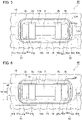
- FIG. 1 is a perspective view of a flexible printed circuit (hereinafter, abbreviated as "FPC") 1 according to the first embodiment.
- FPC flexible printed circuit
- FIG. 1 a portion of the FPC 1 is schematically drawn as an enlarged view in order to clarify a portion where a chip component 2 serving as an electronic component is mounted.
- the FPC 1 is a circuit component for electrically connecting electronic devices to each other, and can be employed in devices in various fields due to having excellent flexibility.
- the FPC 1 may be employed as a vehicle-mounted component in a bus bar module having a plurality of bus bars for connecting respective electrode terminals of adjacent battery cells among a plurality of battery cells included in a battery module.
- the FPC 1 electrically connects the plurality of bus bars in the bus bar module.
- a plurality of electronic components and connectors other than the chip component 2, which is exemplified below, are provided in the other portions of the FPC 1, but these elements will be omitted herein.
- FIGS. 2A and 2B are enlarged schematic views of the mounting portion of the chip component 2 in the FPC 1.
- FIG. 2A is a plan view of the mounting portion.
- FIG. 2B is a cross-sectional view of the mounting portion corresponding to the IIB-IIB cross-section illustrated in FIG. 2A .
- the cross-sectional view illustrated in FIG. 2B is cut along a virtual plane passing through the approximate center of gravity of the chip component 2, and along the mounting direction of the chip component 2 and the direction in which a first electrode 2a and a second electrode 2b of the chip component 2 face each other.
- the mounting direction of the chip component 2 corresponds to a direction perpendicular to the main plane of a base film 10.
- the FPC 1 includes, for example, the chip component 2 serving as an electronic component having two electrodes, the first electrode 2a and the second electrode 2b.
- the chip component 2 is a block body extending in one direction with the first electrode 2a as one end and the second electrode 2b as the other end.
- the chip component 2 may be any electronic component such as a capacitor, a resistor, a coil or a semiconductor.
- the FPC 1 includes the base film 10, a first pattern layer 11 and a second pattern layer 12 constituting a pattern layer, and a coverlay 13.
- the base film 10 is a base portion having excellent flexibility and a planar shape defining the overall shape of the FPC 1.
- the base film 10 is formed of, for example, a polyimide resin excellent in terms of heat resistance.
- the pattern layer is a conductor circuit laminated on a portion of at least one main surface of the base film 10.
- the pattern layer is formed of a material having conductivity, for example, copper foil.
- the first pattern layer 11 and the second pattern layer 12 are exemplified as a pattern layer related to the mounting portion of the chip component 2.
- the pattern 11b is continuous with a portion of the pad 11a and forms a wiring portion over the whole conductor circuit.
- the width of the pattern 11b in the vicinity of the pad 11a is defined as a pattern width WP.
- the pattern width WP is parallel to the pad width W1 and is shorter than the pad width W1.
- the respective centers of the pattern width WP and the pad width W1 coincide with each other in the width direction in which these widths are defined.
- the second pattern layer 12 is a pattern layer connected to the second electrode 2b which is the other electrode of the chip component 2.
- the second pattern layer 12 includes a pad 12a and a pattern 12b.
- the shapes of the pad 12a and the pattern 12b are symmetrical with the shapes of the pad 1 1a and the pattern 11b included in the first pattern layer 11.
- the pad 12a is provided with a bonding region 12d to which the second electrode 2b is soldered.
- the coverlay 13 is a protective layer which is laminated on the entire surface of the base film 10, that is, laminated on the base film 10 or the pattern layer, via an adhesive 14, and protects the pattern layer and the like.
- the adhesive 14 may be an epoxy adhesive containing an epoxy resin having excellent flexibility as a main component.
- the coverlay 13 has an opening 13a for externally exposing the pads 11a and 12a serving as a portion of the pattern layer, and the chip component 2. In order to reduce exposure of the base film 10 and the pattern layer to the outside as much as possible, the shape of an edge 13b of the opening 13a approximately follows the outer peripheral shape of the chip component 2, and the opening 13a does not come into contact with the chip component 2.
- the first electrode 2a is soldered to the pad 11a, and similarly, the second electrode 2b is soldered to the pad 12a.
- the soldering method may be, for example, a reflow method in which solder paste is applied in advance to the bonding region 11d or the like, the first electrode 2a or the like is placed on the applied solder paste, and then the solder paste is melted in a heating furnace to finally bond the objects to each other.
- solder paste is applied in advance to the bonding region 11d or the like
- the first electrode 2a or the like is placed on the applied solder paste, and then the solder paste is melted in a heating furnace to finally bond the objects to each other.
- a fillet 3a bonding the first electrode 2a to the bonding region 11d on the pad 11a and a fillet 3b bonding the second electrode 2b to the bonding region 12d on the pad 12a are drawn as the portions after soldering.
- the pad 11a which is a portion of the first pattern layer 11, has a groove 11c which opens in a range between the bonding region 11d and the edge 13b of the opening 13a in the coverlay 13 on the surface of the pad 11a.
- the pad 12a which is a portion of the second pattern layer 12, has a groove 12c which opens in a range between the bonding region 12d and the edge 13b of the opening 13a on the surface of the pad 12a.
- the groove 11c has the same opening shape as that of the groove 12c.
- the opening shape of the groove 12c is a rectangle in which a groove width LG1 is constant.
- the groove width LG1 is the width in the direction in which the bonding region 12d and the edge 13b of the opening 13a face each other.
- a groove length LG2 which is the length in the direction perpendicular to the groove width LG1, has approximately the same length as the length in the direction in which the bonding region 12d and the edge 13b of the opening 13a face each other. That is, the groove 12c faces the entire bonding region 12d.
- FIG. 3 is an enlarged plan view of a mounting portion of the chip component 2 in an FPC 100 as a comparative example.
- the mounting portion illustrated in FIG. 3 is drawn in accordance with the mounting portion of the chip component 2 in the FPC 1 illustrated in FIG. 2A , the same reference numerals are given to the same portions, and a detailed description thereof will be omitted.
- the shapes of the pads are different from each other, and there are no grooves corresponding to the grooves 11c and 12c in the present embodiment.
- the FPC 100 includes a pad 111a and a pattern 111b in place of the pad 11a and the pattern 11b in the FPC 1.
- a pad length L0 is set to be shorter than the pad length L1 of the pad 11a such that the entire pad 111a is externally exposed from the opening 13a.
- the pad width of the pad 111a may be the same as the pad width W1 of the pad 11a.
- a portion of the pattern 111b continuing with the pad 111a is externally exposed from the opening 13a in the coverlay 13.
- the FPC 100 includes a pad 112a and a pattern 112b in place of the pad 12a and the pattern 12b in the FPC 1.
- the groove 11c is formed in advance in the pad 11a, and similarly, the groove 12c is formed in advance in the pad 12a. Accordingly, even when the adhesive 14 protrudes from the edge 13b and flows out onto the surface of the pad 11a or the pad 12a, the adhesive 14 flows down into the groove 11c or the groove 12c as illustrated in FIGS. 2A and 2B , thereby making it difficult to reach the bonding region 11d or the bonding region 12d.
- the FPC 1 includes an electronic component having an electrode.
- the FPC 1 includes the base film 10, and a conductive pattern layer laminated on a portion of the base film 10 and having a bonding region to which the electrode is soldered.
- the FPC 1 includes the coverlay 13 which is laminated on the base film 10 or the pattern layer via the adhesive 14.
- the coverlay 13 has the opening 13a for externally exposing a portion of the pattern layer including the bonding region, and the electronic component.
- the pattern layer has a groove that opens in a range between the bonding region and the edge 13b of the opening 13a on the surface of the pattern layer.
- the electronic component corresponds to the above chip component 2.
- the electrode corresponds to the above first electrode 2a and the above second electrode 2b.
- the pattern layer corresponds to the above first pattern layer 11 and the above second pattern layer 12.
- the bonding region corresponds to the above bonding region 11d and the above bonding region 12d.
- the groove corresponds to the above groove 11c and the above groove 12c.
- the FPC 1 makes it possible to avoid, in advance, the failure of not being possible for solder paste to be applied to a desired range of the bonding region 11d, thereby causing a defect in soldering thereafter.
- the present embodiment makes it possible to provide the FPC 1 for easily suppressing deterioration in the reliability of soldering when mounting an electronic component.
- the opening 13a is to be set in advance to be large in size such that the protruding adhesive 14 does not easily reach the bonding region 11d.
- setting the opening 13a to be large in size means that the range of the pattern layer exposed from the opening 13a increases, and thus this is undesirable from the viewpoint of protecting the pattern layer.
- the FPC 1 it is only necessary to form the groove 11c in a portion of the pattern layer exposed from the opening portion 13a, and this makes it possible to avoid a large diameter for the opening portion 13a.
- the protruding amount of the adhesive 14 is about 0.2 mm.
- the opening gap between a portion of the pattern layer in which the bonding region 11d is set and the edge 13b of the opening 13a needs to be 0.2 mm or more.
- this opening gap can be set to 0.2 mm or less.
- the groove may face the entire bonding region.
- the FPC 1 makes it possible to guide the adhesive 14 that is about to travel from the edge 13b of the opening 13a to the bonding region 11d via the surface of the pattern layer, to the groove 11c more reliably, thereby making it difficult for the adhesive 14 to reach the bonding region 11d.
- the opening shape of the groove may be a rectangle having a constant width in the direction in which the bonding region and the edge 13b of the opening 13a face each other.
- the FPC 1 makes it possible to easily guide the adhesive 14 to the groove 11c without reaching a position where the adhesive 14 protrudes from the edge 13b of the opening 13a. Further, since the opening shape of the groove is simplified, this is advantageous in avoiding complication of the manufacturing process of the FPC 1.
- the pattern layer may include a pad where a bonding region is set.
- the groove may be formed in the pad.
- the opening shape of the groove 11c can be set to be wide in accordance with the range of the bonding region 11d.
- a portion of the outer peripheral region of the pad faces the bonding region across the groove, and this portion may be positioned below the coverlay 13.
- the opening shape of the groove 11c can be set as wide as possible within a range between the bonding region and the edge 13b of the opening portion 13a.
- a case where a groove such as the groove 11c is formed in a pad such as the pad 11a is exemplified.
- the difference between the pad 11a and the pattern 11b is small in the pattern layer, for example, when the pattern width WP of the pattern 11b continuous with the pad 11a is set in advance to be equal to the pad width W1 of the pad 11a.
- the groove 11c may be formed in the pattern 11b.
- FIG. 4 is an enlarged plan view of a mounting portion of the chip component 2 in an FPC 20 according to the second embodiment.
- the mounting portion illustrated in FIG. 4 is drawn in accordance with the mounting portion of the chip component 2 in the FPC 1 illustrated in FIG. 2A , and the same reference numerals are given to the same portions, and a detailed description thereof will be omitted.
- the FPC 20 includes, instead of the first pattern layer 11 in the FPC 1 according to the first embodiment, a first pattern layer 21 having a pad 21a in which a bonding region 21d is set and a groove 21c is formed and a pattern 21b.
- the FPC 20 includes a second pattern layer 22 having a pad 22a in which a bonding region 22d is set and a groove 22c is formed and a pattern 22b.
- the groove 21c and the groove 22c have the same opening shape.
- the opening shape of the groove 22c is a rectangle in which a groove width LG3 is constant.
- the groove width LG3 is the width in the direction in which the bonding region 22d and the edge 13b of the opening 13a face each other.
- the groove length LG2, which is the length in the direction perpendicular to the groove width LG3, is, for example, the same as the groove length LG2 in the groove 12c in the first embodiment.
- a portion of the groove 21c or the groove 22c in the present embodiment may be positioned below the coverlay 13, unlike the groove 11c or 12c in the first embodiment.
- the groove width LG3 can be set to be large, and thus the opening shape of the groove 21c can be set to be larger. Accordingly, even when the amount of the adhesive 14 protruding from the edge 13b of the opening 13a is relatively large, it is difficult for the adhesive 14 to reach the bonding region 21d.
- FIG. 5 is an enlarged plan view of a mounting portion of the chip component 2 in an FPC 30 according to the third embodiment.
- the mounting portion illustrated in FIG. 5 is drawn in accordance with the mounting portion of the chip component 2 in the FPC 1 illustrated in FIG. 2A , and the same reference numerals are given to the same portions, and a detailed description thereof will be omitted.
- the FPC 30 includes, instead of the first pattern layer 11 in the FPC 1 according to the first embodiment, a first pattern layer 31 having a pad 31a in which a bonding region 31d is set and a groove 31c is formed and a pattern 31b.
- the FPC 30 includes a second pattern layer 32 having a pad 32a in which a bonding region 32d is set and a groove 32c is formed and a pattern 32b.
- the bonding region 31d illustrates a central region 31e where the central portion of the fillet 3a is bonded
- the bonding region 32d illustrates a central region 32e where the central portion of the fillet 3b is bonded.
- the groove 31c and the groove 32c have the same opening shape.
- the opening shape of the groove 32c may be an isosceles triangle having a side facing the bonding region 32d as a base and a side facing the edge 13b of the opening portion 13a as a vertex.
- the length connecting the shortest distance between the vertex and the base is a groove width LG4.
- the groove length LG2 which corresponds to the length of the base, in the direction perpendicular to the groove width LG4 is, for example, the same as the groove length LG2 in the groove 12c of the first embodiment.
- the opening shape of the groove 31c is wider in the portion of the bonding region 31d facing the central region 31e, and narrower toward both ends in the width direction from the central region 31e.
- the groove 31c makes it possible to prevent the adhesive 14 from reaching the central portion of the fillet 3a formed after soldering.
- the suitability of bonding due to soldering is easily affected by whether or not the central portion of the fillet 3a is soldered appropriately. Accordingly, setting the opening shape of the groove 31c to an isosceles triangle as described above makes it possible to prevent the adhesive 14 from reaching at least the central region 31e.
- the isosceles triangles which are the opening shapes of the grooves 31c and 32c, need not be strictly defined by the lengths and angles of the respective sides, and may be slightly modified in a range where the above effect is achieved.
- a portion of the groove 31c and the groove 32c may be positioned below the coverlay 13 as in the second embodiment.
- the shapes of the pads 41a and 42a are different from those of the pads 11a and 12a in the first embodiment.
- the pad 41a has a shape equivalent to that of the pad 11a in the first embodiment only in a portion where the groove 41c is formed so as to face a portion of the bonding region 41d including the central region 41e. Since the remaining portion of the pad 41a does not need to have a groove formed therein, only a shape necessary to secure the bonding region 41d is formed therein.
- the pad length L1 is the same as the pad length L1 in the first embodiment, and the pad width W2 is shorter than the pad width W1 in the first embodiment.
- the pattern 41b is connected within the area of the pad 41a where the groove 41c is formed, and faces the central region 41e of the bonding region 41d.
- the pad width W1 is the same as the pad width W1 in the first embodiment, and the pad length L1 is shorter than the pad length L1 in the first embodiment.
- This area of the pad 41a is not in contact with the edge 13b of the opening 13a.
- the groove 41c and the groove 42c have the same opening shape.
- the groove 42c in FIG. 6 the groove 42c may face a portion of the bonding region 42d including the central region 42e.
- the opening shape of the groove 42c is a rectangle in which a groove width LG6 is constant.
- the groove width LG6 is the width in the direction in which a portion of the bonding region 42d including the central region 42e, and the edge 13b of the opening 13a face each other.
- a groove length LG5 which is the length in the direction perpendicular to the groove width LG6, has a length facing a portion of the bonding region 42d including the central region 42e.
- the groove 41c faces a portion of the bonding region 41d including the central region 41e, the FPC 40 makes it possible to prevent the adhesive 14 from reaching at least the central region 41e as in the third embodiment.
- a portion of the groove 41c and the groove 42c may be positioned below the coverlay 13 as in the second embodiment.
Landscapes
- Engineering & Computer Science (AREA)
- Microelectronics & Electronic Packaging (AREA)
- Manufacturing & Machinery (AREA)
- Structure Of Printed Boards (AREA)
- Electric Connection Of Electric Components To Printed Circuits (AREA)
Abstract
Description
- The present invention relates to a flexible printed circuit.
- Conventionally, there are flexible printed circuits (FPCs) on which chip components serving as electronic components are mounted. Generally, in a flexible printed circuit, a pattern layer serving as a conductor circuit is laminated on a base film. A pattern layer has bonding regions as regions for soldering electrodes of chip components. Further, a coverlay for protecting the pattern layer or the like is laminated on the base film or the pattern layer. A coverlay has openings for externally exposing, for example, bonding regions.
- A coverlay is bonded onto a base film by hot pressing via an adhesive. If the adhesive protrudes from the edge of an opening provided in the coverlay during bonding, the protruding adhesive may reach a bonding region. In this case, a desired bonding region cannot be secured, and as a result, the reliability of soldering may be reduced. Accordingly,
JP 2004-235459 A - The manufacturing method disclosed in
JP 2004-235459 A - An object of the present invention is to provide a flexible printed circuit capable of easily suppressing deterioration in the reliability of soldering when mounting an electronic component.
- A flexible printed circuit of an present invention includes: an electronic component having an electrode; a base film; a conductive pattern layer which is laminated on a portion of the base film and has a bonding region to which the electrode is soldered; and a coverlay laminated on the base film or the pattern layer via an adhesive and having an opening for externally exposing a portion of the pattern layer including the bonding region, and the electronic component. The pattern layer has a groove that opens in a range between the bonding region and an edge of the opening on a surface of the pattern layer.
-
-
FIG. 1 is a perspective view of a flexible printed circuit according to a first embodiment. -
FIG. 2A is a plan view of an electronic component mounting portion in the first embodiment. -
FIG. 2B is a cross-sectional view of the electronic component mounting portion in the first embodiment. -
FIG. 3 is a plan view of an electronic component mounting portion as a comparative example. -
FIG. 4 is a plan view of an electronic component mounting portion in a second embodiment. -
FIG. 5 is a plan view of an electronic component mounting portion in a third embodiment. -
FIG. 6 is a plan view of an electronic component mounting portion in a fourth embodiment. - Various embodiments will be described hereinafter with reference to the accompanying drawings.
- Hereinafter, a flexible printed circuit according to the respective embodiments will be described in detail with reference to the drawings. Dimension ratios of the drawings are exaggerated for convenience of explanation, and may be different from actual ratios.
-
FIG. 1 is a perspective view of a flexible printed circuit (hereinafter, abbreviated as "FPC") 1 according to the first embodiment. InFIG. 1 , a portion of the FPC 1 is schematically drawn as an enlarged view in order to clarify a portion where achip component 2 serving as an electronic component is mounted. - The FPC 1 is a circuit component for electrically connecting electronic devices to each other, and can be employed in devices in various fields due to having excellent flexibility. For example, the FPC 1 may be employed as a vehicle-mounted component in a bus bar module having a plurality of bus bars for connecting respective electrode terminals of adjacent battery cells among a plurality of battery cells included in a battery module. In this case, the FPC 1 electrically connects the plurality of bus bars in the bus bar module. A plurality of electronic components and connectors other than the
chip component 2, which is exemplified below, are provided in the other portions of the FPC 1, but these elements will be omitted herein. -
FIGS. 2A and 2B are enlarged schematic views of the mounting portion of thechip component 2 in theFPC 1.FIG. 2A is a plan view of the mounting portion.FIG. 2B is a cross-sectional view of the mounting portion corresponding to the IIB-IIB cross-section illustrated inFIG. 2A . The cross-sectional view illustrated inFIG. 2B is cut along a virtual plane passing through the approximate center of gravity of thechip component 2, and along the mounting direction of thechip component 2 and the direction in which afirst electrode 2a and asecond electrode 2b of thechip component 2 face each other. Here, the mounting direction of thechip component 2 corresponds to a direction perpendicular to the main plane of abase film 10. - The FPC 1 includes, for example, the
chip component 2 serving as an electronic component having two electrodes, thefirst electrode 2a and thesecond electrode 2b. In the present embodiment, thechip component 2 is a block body extending in one direction with thefirst electrode 2a as one end and thesecond electrode 2b as the other end. Thechip component 2 may be any electronic component such as a capacitor, a resistor, a coil or a semiconductor. - Further, the FPC 1 includes the
base film 10, afirst pattern layer 11 and asecond pattern layer 12 constituting a pattern layer, and acoverlay 13. - The
base film 10 is a base portion having excellent flexibility and a planar shape defining the overall shape of the FPC 1. Thebase film 10 is formed of, for example, a polyimide resin excellent in terms of heat resistance. - The pattern layer is a conductor circuit laminated on a portion of at least one main surface of the
base film 10. The pattern layer is formed of a material having conductivity, for example, copper foil. InFIGS. 1 ,2A and 2B , thefirst pattern layer 11 and thesecond pattern layer 12 are exemplified as a pattern layer related to the mounting portion of thechip component 2. - The
first pattern layer 11 is a pattern layer connected to thefirst electrode 2a, which is one electrode of thechip component 2. Thefirst pattern layer 11 includes apad 11a and apattern 11b. - The
pad 11a is a portion where abonding region 11d to which thefirst electrode 2a is soldered is set. Thepad 11a has a generally rectangular planar shape. Hereinafter, the length along one direction of thepad 11a is defined as a pad length L1, and the width along the other direction perpendicular to one direction of thepad 11a is defined as a pad width W1. In the present embodiment, the above one direction in which the pad length L1 is defined is the same as the direction in which thefirst electrode 2a and thesecond electrode 2b face each other in thechip component 2. - The
pattern 11b is continuous with a portion of thepad 11a and forms a wiring portion over the whole conductor circuit. Hereinafter, the width of thepattern 11b in the vicinity of thepad 11a is defined as a pattern width WP. In the present embodiment, the pattern width WP is parallel to the pad width W1 and is shorter than the pad width W1. The respective centers of the pattern width WP and the pad width W1 coincide with each other in the width direction in which these widths are defined. - The
second pattern layer 12 is a pattern layer connected to thesecond electrode 2b which is the other electrode of thechip component 2. Thesecond pattern layer 12 includes apad 12a and apattern 12b. The shapes of thepad 12a and thepattern 12b are symmetrical with the shapes of thepad 1 1a and thepattern 11b included in thefirst pattern layer 11. Like thepad 11a, thepad 12a is provided with abonding region 12d to which thesecond electrode 2b is soldered. - The
coverlay 13 is a protective layer which is laminated on the entire surface of thebase film 10, that is, laminated on thebase film 10 or the pattern layer, via an adhesive 14, and protects the pattern layer and the like. The adhesive 14 may be an epoxy adhesive containing an epoxy resin having excellent flexibility as a main component. Thecoverlay 13 has anopening 13a for externally exposing thepads chip component 2. In order to reduce exposure of thebase film 10 and the pattern layer to the outside as much as possible, the shape of anedge 13b of theopening 13a approximately follows the outer peripheral shape of thechip component 2, and theopening 13a does not come into contact with thechip component 2. - In mounting the
chip component 2, thefirst electrode 2a is soldered to thepad 11a, and similarly, thesecond electrode 2b is soldered to thepad 12a. The soldering method may be, for example, a reflow method in which solder paste is applied in advance to thebonding region 11d or the like, thefirst electrode 2a or the like is placed on the applied solder paste, and then the solder paste is melted in a heating furnace to finally bond the objects to each other. InFIG. 1 ,FIG. 2A and FIG. 2B , afillet 3a bonding thefirst electrode 2a to thebonding region 11d on thepad 11a and afillet 3b bonding thesecond electrode 2b to thebonding region 12d on thepad 12a are drawn as the portions after soldering. - In the present embodiment, the
pad 11a, which is a portion of thefirst pattern layer 11, has agroove 11c which opens in a range between thebonding region 11d and theedge 13b of theopening 13a in thecoverlay 13 on the surface of thepad 11a. Similarly, thepad 12a, which is a portion of thesecond pattern layer 12, has agroove 12c which opens in a range between thebonding region 12d and theedge 13b of theopening 13a on the surface of thepad 12a. In the present embodiment, thegroove 11c has the same opening shape as that of thegroove 12c. For example, referring to thegroove 12c inFIG. 2A , the opening shape of thegroove 12c is a rectangle in which a groove width LG1 is constant. The groove width LG1 is the width in the direction in which thebonding region 12d and theedge 13b of theopening 13a face each other. Meanwhile, a groove length LG2, which is the length in the direction perpendicular to the groove width LG1, has approximately the same length as the length in the direction in which thebonding region 12d and theedge 13b of theopening 13a face each other. That is, thegroove 12c faces theentire bonding region 12d. - Further, in the present embodiment, the portions of the
respective pads coverlay 13. Specifically, a portion of the outer peripheral region of thepad 11a, which faces thebonding region 11d across thegroove 11c, is positioned below thecoverlay 13. Similarly, a portion of the outer peripheral region of thepad 12a, which faces thebonding region 12d across thegroove 12c, is positioned below thecoverlay 13. Here, "below thecoverlay 13" is not limited to a layer immediately below thecoverlay 13, but refers to layers existing below thecoverlay 13, that is, layers existing below sandwiching the adhesive layer composed of the adhesive 14 in the present embodiment. - Next, the operation of the
FPC 1 will be described. - First, in order to further clarify the operation of the
FPC 1 according to the present embodiment and the effect described later, an FPC as a comparative example will be presented. -
FIG. 3 is an enlarged plan view of a mounting portion of thechip component 2 in anFPC 100 as a comparative example. The mounting portion illustrated inFIG. 3 is drawn in accordance with the mounting portion of thechip component 2 in theFPC 1 illustrated inFIG. 2A , the same reference numerals are given to the same portions, and a detailed description thereof will be omitted. In theFPC 100, as compared with theFPC 1, the shapes of the pads are different from each other, and there are no grooves corresponding to thegrooves - The
FPC 100 includes apad 111a and apattern 111b in place of thepad 11a and thepattern 11b in theFPC 1. In particular, regarding the planar shape of thepad 111a, a pad length L0 is set to be shorter than the pad length L1 of thepad 11a such that theentire pad 111a is externally exposed from theopening 13a. The pad width of thepad 111a may be the same as the pad width W1 of thepad 11a. In this case, a portion of thepattern 111b continuing with thepad 111a is externally exposed from theopening 13a in thecoverlay 13. Similarly, theFPC 100 includes apad 112a and apattern 112b in place of thepad 12a and thepattern 12b in theFPC 1. - Regarding the
FPC 100, a state in which thechip component 2 is not yet mounted will be considered. Thecoverlay 13 is bonded onto thebase film 10 or the pattern layer by heat pressurization via the adhesive 14. This heat pressurization may cause the adhesive 14 to protrude from theedge 13b of theopening 13a toward the inside of theopening 13a. - Here, the region where the pattern layer is not exposed in the
opening 13a is lower than the height positions of thepads edge 13b, it is difficult to reach thebonding region 111d set on thepad 111a, and thebonding region 112d set on thepad 112a. - However, in the region where the pattern layer is exposed in the
opening 13a, theedge 13b of theopening 13a is continuous with thepattern 111b and thepad 111a, and thepattern 112b and thepad 112a. For this reason, if the adhesive 14 protrudes from theedge 13b and flows out onto the surface of thepattern 111b or thepattern 112b, the adhesive 14 may reach thebonding region 111d or thebonding region 112d. For example, as illustrated inFIG. 3 , when thepattern 111b is continuous with thepad 111a toward acentral region 111e of thebonding region 111d, aportion 14a of the adhesive 14 that has flowed onto the surface of thepattern 11 1b is likely to flow into thecentral region 111e. This is also the case in acentral region 112e of thebonding region 112d set on thepad 112a. The inflow of the adhesive 14 into thebonding region 111d or the like leads to narrowing of the range of thebonding region 111d or the like, and as a result, this may reduce the reliability of soldering performed as a later step. - On the other hand, in the
FPC 1 according to the present embodiment, thegroove 11c is formed in advance in thepad 11a, and similarly, thegroove 12c is formed in advance in thepad 12a. Accordingly, even when the adhesive 14 protrudes from theedge 13b and flows out onto the surface of thepad 11a or thepad 12a, the adhesive 14 flows down into thegroove 11c or thegroove 12c as illustrated inFIGS. 2A and 2B , thereby making it difficult to reach thebonding region 11d or thebonding region 12d. - Next, the effect of the
FPC 1 will be described. - The
FPC 1 according to the present embodiment includes an electronic component having an electrode. TheFPC 1 includes thebase film 10, and a conductive pattern layer laminated on a portion of thebase film 10 and having a bonding region to which the electrode is soldered. Further, theFPC 1 includes thecoverlay 13 which is laminated on thebase film 10 or the pattern layer via the adhesive 14. Thecoverlay 13 has theopening 13a for externally exposing a portion of the pattern layer including the bonding region, and the electronic component. The pattern layer has a groove that opens in a range between the bonding region and theedge 13b of theopening 13a on the surface of the pattern layer. - Here, the electronic component corresponds to the
above chip component 2. The electrode corresponds to the abovefirst electrode 2a and the abovesecond electrode 2b. The pattern layer corresponds to the abovefirst pattern layer 11 and the abovesecond pattern layer 12. The bonding region corresponds to theabove bonding region 11d and theabove bonding region 12d. The groove corresponds to theabove groove 11c and theabove groove 12c. - In the following description regarding the effect, the portion relating to the
first pattern layer 11 will be specifically discussed for the sake of simplicity, and the same will be applied to the portion relating to thesecond pattern layer 12. - Even when the adhesive 14 protrudes from the
edge 13b and flows out onto the surface of thepad 11a during the bonding of thecoverlay 13 before thechip component 2 is mounted, the adhesive 14 flows down into thegroove 11c. As a result, this makes it difficult for the adhesive 14 to reach thebonding region 11d set on thepad 11a, and thus, this is less likely to cause the range of thebonding region 11d to be narrowed by the inflow of the adhesive 14 into thebonding region 11d. Accordingly, when thechip component 2 is mounted as a later step, theFPC 1 makes it possible to avoid, in advance, the failure of not being possible for solder paste to be applied to a desired range of thebonding region 11d, thereby causing a defect in soldering thereafter. - Further, as a structure for suppressing the inflow of the adhesive 14 into the bonding region such as the
bonding region 11d, in theFPC 1, only a groove such as thegroove 11c is formed in a portion of the pattern layer exposed from theopening 13a. Accordingly, even when thechip component 2 is small or the number of mountedchip components 2 is large, it is possible to suppress the complexity of the manufacturing process of theFPC 1. - As described above, the present embodiment makes it possible to provide the
FPC 1 for easily suppressing deterioration in the reliability of soldering when mounting an electronic component. - Further, assuming that the adhesive 14 protrudes when the
coverlay 13 is bonded, for example, it is conceivable for theopening 13a is to be set in advance to be large in size such that the protrudingadhesive 14 does not easily reach thebonding region 11d. However, setting theopening 13a to be large in size means that the range of the pattern layer exposed from theopening 13a increases, and thus this is undesirable from the viewpoint of protecting the pattern layer. - Meanwhile, in the
FPC 1, it is only necessary to form thegroove 11c in a portion of the pattern layer exposed from theopening portion 13a, and this makes it possible to avoid a large diameter for theopening portion 13a. For example, when thechip component 2 is small, it is assumed that the protruding amount of the adhesive 14 is about 0.2 mm. In this case, assuming that thegroove 11c does not exist, the opening gap between a portion of the pattern layer in which thebonding region 11d is set and theedge 13b of theopening 13a needs to be 0.2 mm or more. In contrast, in the case of theFPC 1 having thegroove 11c, this opening gap can be set to 0.2 mm or less. - Further, in the
FPC 1 according to the present embodiment, the groove may face the entire bonding region. - For example, the
FPC 1 makes it possible to guide the adhesive 14 that is about to travel from theedge 13b of theopening 13a to thebonding region 11d via the surface of the pattern layer, to thegroove 11c more reliably, thereby making it difficult for the adhesive 14 to reach thebonding region 11d. - In the
FPC 1 according to the present embodiment, the opening shape of the groove may be a rectangle having a constant width in the direction in which the bonding region and theedge 13b of theopening 13a face each other. - The
FPC 1 makes it possible to easily guide the adhesive 14 to thegroove 11c without reaching a position where the adhesive 14 protrudes from theedge 13b of theopening 13a. Further, since the opening shape of the groove is simplified, this is advantageous in avoiding complication of the manufacturing process of theFPC 1. - In the
FPC 1 according to the present embodiment, the pattern layer may include a pad where a bonding region is set. In this case, the groove may be formed in the pad. - According to the
FPC 1, for example, since thegroove 11c is formed in thepad 11a where thebonding region 11d is set, the opening shape of thegroove 11c can be set to be wide in accordance with the range of thebonding region 11d. - In the
FPC 1 according to the present embodiment, a portion of the outer peripheral region of the pad faces the bonding region across the groove, and this portion may be positioned below thecoverlay 13. - According to the
FPC 1, for example, since thegroove 11c can be formed at a position corresponding to theedge 13b of theopening portion 13a, the opening shape of thegroove 11c can be set as wide as possible within a range between the bonding region and theedge 13b of theopening portion 13a. - In the description using the above figures, a case where a groove such as the
groove 11c is formed in a pad such as thepad 11a is exemplified. However, there may be a case where the difference between thepad 11a and thepattern 11b is small in the pattern layer, for example, when the pattern width WP of thepattern 11b continuous with thepad 11a is set in advance to be equal to the pad width W1 of thepad 11a. In such a case, thegroove 11c may be formed in thepattern 11b. -
FIG. 4 is an enlarged plan view of a mounting portion of thechip component 2 in anFPC 20 according to the second embodiment. The mounting portion illustrated inFIG. 4 is drawn in accordance with the mounting portion of thechip component 2 in theFPC 1 illustrated inFIG. 2A , and the same reference numerals are given to the same portions, and a detailed description thereof will be omitted. - The
FPC 20 includes, instead of thefirst pattern layer 11 in theFPC 1 according to the first embodiment, afirst pattern layer 21 having apad 21a in which abonding region 21d is set and agroove 21c is formed and apattern 21b. Similarly, instead of thesecond pattern layer 12 in theFPC 1 according to the first embodiment, theFPC 20 includes asecond pattern layer 22 having apad 22a in which abonding region 22d is set and agroove 22c is formed and apattern 22b. - In the present embodiment, the
groove 21c and thegroove 22c have the same opening shape. For example, referring to thegroove 22c inFIG. 4 , the opening shape of thegroove 22c is a rectangle in which a groove width LG3 is constant. The groove width LG3 is the width in the direction in which thebonding region 22d and theedge 13b of theopening 13a face each other. Meanwhile, the groove length LG2, which is the length in the direction perpendicular to the groove width LG3, is, for example, the same as the groove length LG2 in thegroove 12c in the first embodiment. - A portion of the
groove 21c or thegroove 22c in the present embodiment may be positioned below thecoverlay 13, unlike thegroove - According to the
FPC 20, referring to thegroove 21c as a representative example, as can be seen from the comparison of the groove width LG1 of thegroove 1 1c in the first embodiment, the groove width LG3 can be set to be large, and thus the opening shape of thegroove 21c can be set to be larger. Accordingly, even when the amount of the adhesive 14 protruding from theedge 13b of theopening 13a is relatively large, it is difficult for the adhesive 14 to reach thebonding region 21d. -
FIG. 5 is an enlarged plan view of a mounting portion of thechip component 2 in anFPC 30 according to the third embodiment. The mounting portion illustrated inFIG. 5 is drawn in accordance with the mounting portion of thechip component 2 in theFPC 1 illustrated inFIG. 2A , and the same reference numerals are given to the same portions, and a detailed description thereof will be omitted. - The
FPC 30 includes, instead of thefirst pattern layer 11 in theFPC 1 according to the first embodiment, afirst pattern layer 31 having a pad 31a in which abonding region 31d is set and agroove 31c is formed and apattern 31b. Similarly, instead of thesecond pattern layer 12 in theFPC 1 according to the first embodiment, theFPC 30 includes asecond pattern layer 32 having apad 32a in which abonding region 32d is set and agroove 32c is formed and apattern 32b. InFIG. 5 , thebonding region 31d illustrates a central region 31e where the central portion of thefillet 3a is bonded, and thebonding region 32d illustrates acentral region 32e where the central portion of thefillet 3b is bonded. - In the present embodiment, the
groove 31c and thegroove 32c have the same opening shape. For example, referring to thegroove 32c inFIG. 5 , the opening shape of thegroove 32c may be an isosceles triangle having a side facing thebonding region 32d as a base and a side facing theedge 13b of theopening portion 13a as a vertex. In this case, the length connecting the shortest distance between the vertex and the base is a groove width LG4. Meanwhile, the groove length LG2, which corresponds to the length of the base, in the direction perpendicular to the groove width LG4 is, for example, the same as the groove length LG2 in thegroove 12c of the first embodiment. - According to the
FPC 30, referring to thegroove 31c as a representative example, the opening shape of thegroove 31c is wider in the portion of thebonding region 31d facing the central region 31e, and narrower toward both ends in the width direction from the central region 31e. Thegroove 31c makes it possible to prevent the adhesive 14 from reaching the central portion of thefillet 3a formed after soldering. The suitability of bonding due to soldering is easily affected by whether or not the central portion of thefillet 3a is soldered appropriately. Accordingly, setting the opening shape of thegroove 31c to an isosceles triangle as described above makes it possible to prevent the adhesive 14 from reaching at least the central region 31e. - It should be noted that the isosceles triangles, which are the opening shapes of the
grooves groove 31c and thegroove 32c may be positioned below thecoverlay 13 as in the second embodiment. -
FIG. 6 is an enlarged plan view of a mounting portion of thechip component 2 in anFPC 40 according to the fourth embodiment. The mounting portion illustrated inFIG. 6 is drawn in accordance with the mounting portion of thechip component 2 in theFPC 1 illustrated inFIG. 2A , and the same reference numerals are given to the same portions, and a detailed description thereof will be omitted. - The
FPC 40 includes, instead of thefirst pattern layer 11 in theFPC 1 according to the first embodiment, afirst pattern layer 41 having apad 41a in which abonding region 41d is set and agroove 41c is formed and apattern 41b. Similarly, instead of thesecond pattern layer 12 in theFPC 1 according to the first embodiment, theFPC 40 includes asecond pattern layer 42 having apad 42a in which abonding region 42d is set and agroove 42c is formed and apattern 42b. InFIG. 6 , thebonding region 41d illustrates acentral region 41e where the central portion of thefillet 3a is bonded, and thebonding region 42d illustrates acentral region 42e where the central portion of thefillet 3b is bonded. - In the present embodiment, the shapes of the
pads pads pad 41a as a representative example, thepad 41a has a shape equivalent to that of thepad 11a in the first embodiment only in a portion where thegroove 41c is formed so as to face a portion of thebonding region 41d including thecentral region 41e. Since the remaining portion of thepad 41a does not need to have a groove formed therein, only a shape necessary to secure thebonding region 41d is formed therein. - For example, in the area of the
pad 41a where thegroove 41c is formed, the pad length L1 is the same as the pad length L1 in the first embodiment, and the pad width W2 is shorter than the pad width W1 in the first embodiment. Further, thepattern 41b is connected within the area of thepad 41a where thegroove 41c is formed, and faces thecentral region 41e of thebonding region 41d. - Meanwhile, in the other area of the
pad 41a, the pad width W1 is the same as the pad width W1 in the first embodiment, and the pad length L1 is shorter than the pad length L1 in the first embodiment. This area of thepad 41a is not in contact with theedge 13b of theopening 13a. - In the present embodiment, the
groove 41c and thegroove 42c have the same opening shape. For example, referring to thegroove 42c inFIG. 6 , thegroove 42c may face a portion of thebonding region 42d including thecentral region 42e. Specifically, the opening shape of thegroove 42c is a rectangle in which a groove width LG6 is constant. The groove width LG6 is the width in the direction in which a portion of thebonding region 42d including thecentral region 42e, and theedge 13b of theopening 13a face each other. Meanwhile, a groove length LG5, which is the length in the direction perpendicular to the groove width LG6, has a length facing a portion of thebonding region 42d including thecentral region 42e. In other words, according to the specification of thegroove 42c in the present embodiment, the opening shape of thegroove 42c can be set such that a portion of thegroove 42c faces thecentral region 42e and approaches one end side in the width direction of thepad 42a, as illustrated inFIG. 6 . - Referring to the
groove 41c as a representative example, thegroove 41c faces a portion of thebonding region 41d including thecentral region 41e, theFPC 40 makes it possible to prevent the adhesive 14 from reaching at least thecentral region 41e as in the third embodiment. - A portion of the
groove 41c and thegroove 42c may be positioned below thecoverlay 13 as in the second embodiment. - Although the present invention has been described above by reference to the embodiment, the present invention is not limited to those and the configuration of parts can be replaced with any configuration having a similar function, as long as they lie within the scope of the claims.
Claims (9)
- A flexible printed circuit (1, 20, 30, 40) comprising:an electronic component (2) having an electrode (2a, 2b);a base film (10);a conductive pattern layer (11, 12, 21, 22, 31, 32, 41, 42) which is laminated on a portion of the base film and has a bonding region (11d, 12d, 21d, 22d, 31d, 32d, 41d, 42d) to which the electrode (2a, 2b) is soldered; anda coverlay (13) laminated on the base film (10) or the pattern layer (11, 12, 21, 22, 31, 32, 41, 42) via an adhesive (14) and having an opening (13a) for externally exposing a portion of the pattern layer (11, 12, 21, 22, 31, 32, 41, 42) including the bonding region (11d, 12d, 21d, 22d, 31d, 32d, 41d, 42d), and the electronic component (2), whereinthe pattern layer (11, 12, 21, 22, 31, 32, 41, 42) has a groove (11c, 12c, 21c, 22c, 31c, 32c, 41c, 42c) that opens in a range between the bonding region (11d, 12d, 21d, 22d, 31d, 32d, 41d, 42d) and an edge (13b) of the opening (13a) on a surface of the pattern layer (11, 12, 21, 22, 31, 32, 41, 42).
- The flexible printed circuit (20) according claim 1, wherein
a portion of the groove (21c, 22c) is positioned below the coverlay (13). - The flexible printed circuit (10, 20, 30) according claim 1 or 2, wherein
the groove (11c, 12c, 21c, 22c, 31c, 32c) faces the entire bonding region (11d, 12d, 21d, 22d, 31d, 32d). - The flexible printed circuit (30, 40) according claim 1 or 2, wherein
the groove (31c, 32c, 41c, 42c) faces a portion of the bonding region (31d, 32d, 41d, 42d) including a central region (31e, 32e, 41e, 42e). - The flexible printed circuit (1, 20, 40) according to any one of claims 1 to 4, wherein
an opening shape of the groove (11c, 12c, 21c, 22c, 41c, 42c) is a rectangle having a constant width in a direction in which the bonding region (11d, 12d, 21d, 22d, 41d, 42d) and the edge (13b) of the opening (13a) face each other. - The flexible printed circuit (30) according to any one of claims 1 to 4, wherein
an opening shape of the groove (31c, 32c) is an isosceles triangle having a side facing the bonding region (31d, 32d) as a base and a side facing the edge (13b) of the opening (13a) as a vertex. - The flexible printed circuit (1, 20, 30, 40) according to any one of claims 1 to 6, whereinthe pattern layer (11, 12, 21, 22, 31, 32, 41, 42) includes a pad (11a, 12a, 21a, 22a, 31a, 32a, 41a, 42a) where the bonding region (11d, 12d, 21d, 22d, 31d, 32d, 41d, 42d) is set, andthe groove (11c, 12c, 21c, 22c, 31c, 32c, 41c, 42c) is formed in the pad (11a, 12a, 21a, 22a, 31a, 32a, 41a, 42a).
- The flexible printed circuit (1, 20, 30, 40) according claim 7, wherein
a portion of an outer peripheral region of the pad (11a, 12a, 21a, 22a, 31a, 32a, 41a, 42a) faces the bonding region (11d, 12d, 21d, 22d, 31d, 32d, 41d, 42d) across the groove (11c, 12c, 21c, 22c, 31c, 32c, 41c, 42c) and is positioned below the coverlay (13). - The flexible printed circuit (1, 20, 30, 40) according to any one of claims 1 to 8, wherein
the flexible printed circuit (1, 20, 30, 40) is included in a bus bar module having a plurality of bus bars for connecting respective electrode terminals of adjacent battery cells, and electrically connects the plurality of bus bars.
Applications Claiming Priority (1)
| Application Number | Priority Date | Filing Date | Title |
|---|---|---|---|
| JP2021108723A JP7456977B2 (en) | 2021-06-30 | 2021-06-30 | Flexible Printed Wiring Boards |
Publications (2)
| Publication Number | Publication Date |
|---|---|
| EP4114148A1 true EP4114148A1 (en) | 2023-01-04 |
| EP4114148B1 EP4114148B1 (en) | 2024-01-17 |
Family
ID=82492669
Family Applications (1)
| Application Number | Title | Priority Date | Filing Date |
|---|---|---|---|
| EP22182036.8A Active EP4114148B1 (en) | 2021-06-30 | 2022-06-29 | Flexible printed circuit |
Country Status (4)
| Country | Link |
|---|---|
| US (1) | US11950368B2 (en) |
| EP (1) | EP4114148B1 (en) |
| JP (1) | JP7456977B2 (en) |
| CN (1) | CN115551197A (en) |
Families Citing this family (1)
| Publication number | Priority date | Publication date | Assignee | Title |
|---|---|---|---|---|
| JP7439001B2 (en) * | 2021-02-19 | 2024-02-27 | 矢崎総業株式会社 | Flexible printed circuit board, flexible printed circuit board manufacturing method |
Citations (4)
| Publication number | Priority date | Publication date | Assignee | Title |
|---|---|---|---|---|
| JP2004235459A (en) | 2003-01-30 | 2004-08-19 | Fujikura Ltd | Manufacturing method of flexible printed wiring board |
| JP2005085807A (en) * | 2003-09-04 | 2005-03-31 | Seiko Epson Corp | WIRING BOARD AND MANUFACTURING METHOD THEREOF, ELECTRO-OPTICAL DEVICE, ELECTRONIC DEVICE |
| US20170265299A1 (en) * | 2016-03-08 | 2017-09-14 | Ibiden Co., Ltd. | Wiring board and method for manufacturing the same |
| US20200274204A1 (en) * | 2019-02-26 | 2020-08-27 | GM Global Technology Operations LLC | Battery module with interconnect board assembly having integrated cell sense pcb-flex circuit hardware |
Family Cites Families (10)
| Publication number | Priority date | Publication date | Assignee | Title |
|---|---|---|---|---|
| KR100729080B1 (en) * | 2000-12-29 | 2007-06-14 | 앰코 테크놀로지 코리아 주식회사 | Printed Circuit Boards and Semiconductor Packages Using the Same |
| JP2007180397A (en) | 2005-12-28 | 2007-07-12 | Sharp Corp | Printed wiring board and liquid crystal display device |
| JP2008277340A (en) | 2007-04-25 | 2008-11-13 | Denso Corp | Wiring metal plate |
| JP5509893B2 (en) | 2010-02-04 | 2014-06-04 | 三菱電機株式会社 | Circuit board and manufacturing method thereof |
| JP5752727B2 (en) | 2013-02-27 | 2015-07-22 | 株式会社フジクラ | Component mounting flexible printed circuit board |
| US8998454B2 (en) * | 2013-03-15 | 2015-04-07 | Sumitomo Electric Printed Circuits, Inc. | Flexible electronic assembly and method of manufacturing the same |
| JP6578735B2 (en) * | 2014-05-21 | 2019-09-25 | 日亜化学工業株式会社 | Semiconductor device mounting structure, backlight device, and mounting substrate |
| CN205752172U (en) * | 2016-05-17 | 2016-11-30 | 歌尔股份有限公司 | A kind of optical sensor package structure |
| JP2018207070A (en) | 2017-06-09 | 2018-12-27 | イビデン株式会社 | Printed wiring board and its manufacturing method |
| KR102421009B1 (en) * | 2018-01-02 | 2022-07-14 | 삼성디스플레이 주식회사 | Display device |
-
2021
- 2021-06-30 JP JP2021108723A patent/JP7456977B2/en active Active
-
2022
- 2022-06-28 US US17/851,504 patent/US11950368B2/en active Active
- 2022-06-29 EP EP22182036.8A patent/EP4114148B1/en active Active
- 2022-06-30 CN CN202210767385.9A patent/CN115551197A/en active Pending
Patent Citations (4)
| Publication number | Priority date | Publication date | Assignee | Title |
|---|---|---|---|---|
| JP2004235459A (en) | 2003-01-30 | 2004-08-19 | Fujikura Ltd | Manufacturing method of flexible printed wiring board |
| JP2005085807A (en) * | 2003-09-04 | 2005-03-31 | Seiko Epson Corp | WIRING BOARD AND MANUFACTURING METHOD THEREOF, ELECTRO-OPTICAL DEVICE, ELECTRONIC DEVICE |
| US20170265299A1 (en) * | 2016-03-08 | 2017-09-14 | Ibiden Co., Ltd. | Wiring board and method for manufacturing the same |
| US20200274204A1 (en) * | 2019-02-26 | 2020-08-27 | GM Global Technology Operations LLC | Battery module with interconnect board assembly having integrated cell sense pcb-flex circuit hardware |
Also Published As
| Publication number | Publication date |
|---|---|
| JP7456977B2 (en) | 2024-03-27 |
| US20230007779A1 (en) | 2023-01-05 |
| CN115551197A (en) | 2022-12-30 |
| US11950368B2 (en) | 2024-04-02 |
| EP4114148B1 (en) | 2024-01-17 |
| JP2023006225A (en) | 2023-01-18 |
Similar Documents
| Publication | Publication Date | Title |
|---|---|---|
| KR100299949B1 (en) | Thin type semiconductor device, module structure using the device and method of mounting the device on board | |
| US20140252613A1 (en) | Semiconductor device | |
| JP3640155B2 (en) | Flexible wiring board, film carrier, tape-like semiconductor device, semiconductor device, circuit board, and electronic device | |
| CN100459115C (en) | Tape circuit substrate and semiconductor chip package using same | |
| US7660132B2 (en) | Covered multilayer module | |
| KR102620302B1 (en) | Flexible Printed Circuit Board and Manufacturing Method thereof | |
| JPH11233684A (en) | Semiconductor device substrate, semiconductor device, method of manufacturing the same, and electronic equipment | |
| US20110007482A1 (en) | Printed circuit board unit and electronic device | |
| EP2086296B1 (en) | Printed circuit board and method of manufacturing the same | |
| EP4114148B1 (en) | Flexible printed circuit | |
| US9629249B2 (en) | Component-embedded substrate and communication module | |
| CN107958875B (en) | Semiconductor device and wiring substrate design method | |
| JP7558604B1 (en) | Multilayer board manufacturing method | |
| JPH11340609A (en) | Manufacture of printed wiring board and manufacture of unit wiring board | |
| JP2001251057A (en) | Apparatus in which device is mounted on multilayer printed wiring board, multilayer printed wiring board, and device | |
| CN112822838B (en) | Connecting structure including circuit body and conductive body | |
| WO2012172890A1 (en) | Printed-wiring board, electronic-component mounting structure, and method for manufacturing electronic-component mounting structure | |
| CN114143980A (en) | Circuit board connection structure and manufacturing method thereof | |
| US10188000B2 (en) | Component mounting board | |
| JP4072415B2 (en) | Flexible circuit board | |
| CN101436588A (en) | Circuit module | |
| CN119275200A (en) | COF type semiconductor packaging device and manufacturing method thereof | |
| JP2026067604A (en) | Electronic terminal device, substrate, and method for manufacturing an electronic terminal device | |
| KR20250118160A (en) | Printed circuit board | |
| JP2005223129A (en) | Coil system |
Legal Events
| Date | Code | Title | Description |
|---|---|---|---|
| PUAI | Public reference made under article 153(3) epc to a published international application that has entered the european phase |
Free format text: ORIGINAL CODE: 0009012 |
|
| STAA | Information on the status of an ep patent application or granted ep patent |
Free format text: STATUS: REQUEST FOR EXAMINATION WAS MADE |
|
| 17P | Request for examination filed |
Effective date: 20220629 |
|
| AK | Designated contracting states |
Kind code of ref document: A1 Designated state(s): AL AT BE BG CH CY CZ DE DK EE ES FI FR GB GR HR HU IE IS IT LI LT LU LV MC MK MT NL NO PL PT RO RS SE SI SK SM TR |
|
| RBV | Designated contracting states (corrected) |
Designated state(s): AL AT BE BG CH CY CZ DE DK EE ES FI FR GB GR HR HU IE IS IT LI LT LU LV MC MK MT NL NO PL PT RO RS SE SI SK SM TR |
|
| STAA | Information on the status of an ep patent application or granted ep patent |
Free format text: STATUS: EXAMINATION IS IN PROGRESS |
|
| RAP3 | Party data changed (applicant data changed or rights of an application transferred) |
Owner name: YAZAKI CORPORATION |
|
| 17Q | First examination report despatched |
Effective date: 20230517 |
|
| GRAP | Despatch of communication of intention to grant a patent |
Free format text: ORIGINAL CODE: EPIDOSNIGR1 |
|
| STAA | Information on the status of an ep patent application or granted ep patent |
Free format text: STATUS: GRANT OF PATENT IS INTENDED |
|
| RIC1 | Information provided on ipc code assigned before grant |
Ipc: H05K 1/11 20060101ALN20231012BHEP Ipc: H05K 3/34 20060101ALI20231012BHEP Ipc: H05K 3/28 20060101ALI20231012BHEP Ipc: H05K 1/18 20060101AFI20231012BHEP |
|
| RIC1 | Information provided on ipc code assigned before grant |
Ipc: H05K 1/11 20060101ALN20231017BHEP Ipc: H05K 3/34 20060101ALI20231017BHEP Ipc: H05K 3/28 20060101ALI20231017BHEP Ipc: H05K 1/18 20060101AFI20231017BHEP |
|
| INTG | Intention to grant announced |
Effective date: 20231030 |
|
| GRAS | Grant fee paid |
Free format text: ORIGINAL CODE: EPIDOSNIGR3 |
|
| GRAA | (expected) grant |
Free format text: ORIGINAL CODE: 0009210 |
|
| STAA | Information on the status of an ep patent application or granted ep patent |
Free format text: STATUS: THE PATENT HAS BEEN GRANTED |
|
| AK | Designated contracting states |
Kind code of ref document: B1 Designated state(s): AL AT BE BG CH CY CZ DE DK EE ES FI FR GB GR HR HU IE IS IT LI LT LU LV MC MK MT NL NO PL PT RO RS SE SI SK SM TR |
|
| REG | Reference to a national code |
Ref country code: GB Ref legal event code: FG4D |
|
| REG | Reference to a national code |
Ref country code: DE Ref legal event code: R096 Ref document number: 602022001603 Country of ref document: DE |
|
| REG | Reference to a national code |
Ref country code: CH Ref legal event code: EP |
|
| REG | Reference to a national code |
Ref country code: IE Ref legal event code: FG4D |
|
| REG | Reference to a national code |
Ref country code: LT Ref legal event code: MG9D |
|
| REG | Reference to a national code |
Ref country code: NL Ref legal event code: MP Effective date: 20240117 |
|
| REG | Reference to a national code |
Ref country code: AT Ref legal event code: MK05 Ref document number: 1651387 Country of ref document: AT Kind code of ref document: T Effective date: 20240117 |
|
| PG25 | Lapsed in a contracting state [announced via postgrant information from national office to epo] |
Ref country code: NL Free format text: LAPSE BECAUSE OF FAILURE TO SUBMIT A TRANSLATION OF THE DESCRIPTION OR TO PAY THE FEE WITHIN THE PRESCRIBED TIME-LIMIT Effective date: 20240117 |
|
| PG25 | Lapsed in a contracting state [announced via postgrant information from national office to epo] |
Ref country code: NL Free format text: LAPSE BECAUSE OF FAILURE TO SUBMIT A TRANSLATION OF THE DESCRIPTION OR TO PAY THE FEE WITHIN THE PRESCRIBED TIME-LIMIT Effective date: 20240117 |
|
| PG25 | Lapsed in a contracting state [announced via postgrant information from national office to epo] |
Ref country code: IS Free format text: LAPSE BECAUSE OF FAILURE TO SUBMIT A TRANSLATION OF THE DESCRIPTION OR TO PAY THE FEE WITHIN THE PRESCRIBED TIME-LIMIT Effective date: 20240517 |
|
| PG25 | Lapsed in a contracting state [announced via postgrant information from national office to epo] |
Ref country code: LT Free format text: LAPSE BECAUSE OF FAILURE TO SUBMIT A TRANSLATION OF THE DESCRIPTION OR TO PAY THE FEE WITHIN THE PRESCRIBED TIME-LIMIT Effective date: 20240117 |
|
| PG25 | Lapsed in a contracting state [announced via postgrant information from national office to epo] |
Ref country code: GR Free format text: LAPSE BECAUSE OF FAILURE TO SUBMIT A TRANSLATION OF THE DESCRIPTION OR TO PAY THE FEE WITHIN THE PRESCRIBED TIME-LIMIT Effective date: 20240418 |
|
| PG25 | Lapsed in a contracting state [announced via postgrant information from national office to epo] |
Ref country code: RS Free format text: LAPSE BECAUSE OF FAILURE TO SUBMIT A TRANSLATION OF THE DESCRIPTION OR TO PAY THE FEE WITHIN THE PRESCRIBED TIME-LIMIT Effective date: 20240417 Ref country code: HR Free format text: LAPSE BECAUSE OF FAILURE TO SUBMIT A TRANSLATION OF THE DESCRIPTION OR TO PAY THE FEE WITHIN THE PRESCRIBED TIME-LIMIT Effective date: 20240117 |
|
| PG25 | Lapsed in a contracting state [announced via postgrant information from national office to epo] |
Ref country code: ES Free format text: LAPSE BECAUSE OF FAILURE TO SUBMIT A TRANSLATION OF THE DESCRIPTION OR TO PAY THE FEE WITHIN THE PRESCRIBED TIME-LIMIT Effective date: 20240117 |
|
| PG25 | Lapsed in a contracting state [announced via postgrant information from national office to epo] |
Ref country code: AT Free format text: LAPSE BECAUSE OF FAILURE TO SUBMIT A TRANSLATION OF THE DESCRIPTION OR TO PAY THE FEE WITHIN THE PRESCRIBED TIME-LIMIT Effective date: 20240117 |
|
| PG25 | Lapsed in a contracting state [announced via postgrant information from national office to epo] |
Ref country code: RS Free format text: LAPSE BECAUSE OF FAILURE TO SUBMIT A TRANSLATION OF THE DESCRIPTION OR TO PAY THE FEE WITHIN THE PRESCRIBED TIME-LIMIT Effective date: 20240417 Ref country code: NO Free format text: LAPSE BECAUSE OF FAILURE TO SUBMIT A TRANSLATION OF THE DESCRIPTION OR TO PAY THE FEE WITHIN THE PRESCRIBED TIME-LIMIT Effective date: 20240417 Ref country code: LT Free format text: LAPSE BECAUSE OF FAILURE TO SUBMIT A TRANSLATION OF THE DESCRIPTION OR TO PAY THE FEE WITHIN THE PRESCRIBED TIME-LIMIT Effective date: 20240117 Ref country code: IS Free format text: LAPSE BECAUSE OF FAILURE TO SUBMIT A TRANSLATION OF THE DESCRIPTION OR TO PAY THE FEE WITHIN THE PRESCRIBED TIME-LIMIT Effective date: 20240517 Ref country code: HR Free format text: LAPSE BECAUSE OF FAILURE TO SUBMIT A TRANSLATION OF THE DESCRIPTION OR TO PAY THE FEE WITHIN THE PRESCRIBED TIME-LIMIT Effective date: 20240117 Ref country code: GR Free format text: LAPSE BECAUSE OF FAILURE TO SUBMIT A TRANSLATION OF THE DESCRIPTION OR TO PAY THE FEE WITHIN THE PRESCRIBED TIME-LIMIT Effective date: 20240418 Ref country code: FI Free format text: LAPSE BECAUSE OF FAILURE TO SUBMIT A TRANSLATION OF THE DESCRIPTION OR TO PAY THE FEE WITHIN THE PRESCRIBED TIME-LIMIT Effective date: 20240117 Ref country code: ES Free format text: LAPSE BECAUSE OF FAILURE TO SUBMIT A TRANSLATION OF THE DESCRIPTION OR TO PAY THE FEE WITHIN THE PRESCRIBED TIME-LIMIT Effective date: 20240117 Ref country code: BG Free format text: LAPSE BECAUSE OF FAILURE TO SUBMIT A TRANSLATION OF THE DESCRIPTION OR TO PAY THE FEE WITHIN THE PRESCRIBED TIME-LIMIT Effective date: 20240117 Ref country code: AT Free format text: LAPSE BECAUSE OF FAILURE TO SUBMIT A TRANSLATION OF THE DESCRIPTION OR TO PAY THE FEE WITHIN THE PRESCRIBED TIME-LIMIT Effective date: 20240117 |
|
| PG25 | Lapsed in a contracting state [announced via postgrant information from national office to epo] |
Ref country code: PT Free format text: LAPSE BECAUSE OF FAILURE TO SUBMIT A TRANSLATION OF THE DESCRIPTION OR TO PAY THE FEE WITHIN THE PRESCRIBED TIME-LIMIT Effective date: 20240517 Ref country code: PL Free format text: LAPSE BECAUSE OF FAILURE TO SUBMIT A TRANSLATION OF THE DESCRIPTION OR TO PAY THE FEE WITHIN THE PRESCRIBED TIME-LIMIT Effective date: 20240117 |
|
| PG25 | Lapsed in a contracting state [announced via postgrant information from national office to epo] |
Ref country code: SE Free format text: LAPSE BECAUSE OF FAILURE TO SUBMIT A TRANSLATION OF THE DESCRIPTION OR TO PAY THE FEE WITHIN THE PRESCRIBED TIME-LIMIT Effective date: 20240117 Ref country code: PT Free format text: LAPSE BECAUSE OF FAILURE TO SUBMIT A TRANSLATION OF THE DESCRIPTION OR TO PAY THE FEE WITHIN THE PRESCRIBED TIME-LIMIT Effective date: 20240517 Ref country code: PL Free format text: LAPSE BECAUSE OF FAILURE TO SUBMIT A TRANSLATION OF THE DESCRIPTION OR TO PAY THE FEE WITHIN THE PRESCRIBED TIME-LIMIT Effective date: 20240117 Ref country code: LV Free format text: LAPSE BECAUSE OF FAILURE TO SUBMIT A TRANSLATION OF THE DESCRIPTION OR TO PAY THE FEE WITHIN THE PRESCRIBED TIME-LIMIT Effective date: 20240117 |
|
| PG25 | Lapsed in a contracting state [announced via postgrant information from national office to epo] |
Ref country code: DK Free format text: LAPSE BECAUSE OF FAILURE TO SUBMIT A TRANSLATION OF THE DESCRIPTION OR TO PAY THE FEE WITHIN THE PRESCRIBED TIME-LIMIT Effective date: 20240117 |
|
| PG25 | Lapsed in a contracting state [announced via postgrant information from national office to epo] |
Ref country code: SM Free format text: LAPSE BECAUSE OF FAILURE TO SUBMIT A TRANSLATION OF THE DESCRIPTION OR TO PAY THE FEE WITHIN THE PRESCRIBED TIME-LIMIT Effective date: 20240117 |
|
| REG | Reference to a national code |
Ref country code: DE Ref legal event code: R097 Ref document number: 602022001603 Country of ref document: DE |
|
| PG25 | Lapsed in a contracting state [announced via postgrant information from national office to epo] |
Ref country code: EE Free format text: LAPSE BECAUSE OF FAILURE TO SUBMIT A TRANSLATION OF THE DESCRIPTION OR TO PAY THE FEE WITHIN THE PRESCRIBED TIME-LIMIT Effective date: 20240117 Ref country code: CZ Free format text: LAPSE BECAUSE OF FAILURE TO SUBMIT A TRANSLATION OF THE DESCRIPTION OR TO PAY THE FEE WITHIN THE PRESCRIBED TIME-LIMIT Effective date: 20240117 |
|
| PG25 | Lapsed in a contracting state [announced via postgrant information from national office to epo] |
Ref country code: SK Free format text: LAPSE BECAUSE OF FAILURE TO SUBMIT A TRANSLATION OF THE DESCRIPTION OR TO PAY THE FEE WITHIN THE PRESCRIBED TIME-LIMIT Effective date: 20240117 |
|
| PG25 | Lapsed in a contracting state [announced via postgrant information from national office to epo] |
Ref country code: SM Free format text: LAPSE BECAUSE OF FAILURE TO SUBMIT A TRANSLATION OF THE DESCRIPTION OR TO PAY THE FEE WITHIN THE PRESCRIBED TIME-LIMIT Effective date: 20240117 Ref country code: SK Free format text: LAPSE BECAUSE OF FAILURE TO SUBMIT A TRANSLATION OF THE DESCRIPTION OR TO PAY THE FEE WITHIN THE PRESCRIBED TIME-LIMIT Effective date: 20240117 Ref country code: RO Free format text: LAPSE BECAUSE OF FAILURE TO SUBMIT A TRANSLATION OF THE DESCRIPTION OR TO PAY THE FEE WITHIN THE PRESCRIBED TIME-LIMIT Effective date: 20240117 Ref country code: EE Free format text: LAPSE BECAUSE OF FAILURE TO SUBMIT A TRANSLATION OF THE DESCRIPTION OR TO PAY THE FEE WITHIN THE PRESCRIBED TIME-LIMIT Effective date: 20240117 Ref country code: DK Free format text: LAPSE BECAUSE OF FAILURE TO SUBMIT A TRANSLATION OF THE DESCRIPTION OR TO PAY THE FEE WITHIN THE PRESCRIBED TIME-LIMIT Effective date: 20240117 Ref country code: CZ Free format text: LAPSE BECAUSE OF FAILURE TO SUBMIT A TRANSLATION OF THE DESCRIPTION OR TO PAY THE FEE WITHIN THE PRESCRIBED TIME-LIMIT Effective date: 20240117 |
|
| PLBE | No opposition filed within time limit |
Free format text: ORIGINAL CODE: 0009261 |
|
| STAA | Information on the status of an ep patent application or granted ep patent |
Free format text: STATUS: NO OPPOSITION FILED WITHIN TIME LIMIT |
|
| PG25 | Lapsed in a contracting state [announced via postgrant information from national office to epo] |
Ref country code: IT Free format text: LAPSE BECAUSE OF FAILURE TO SUBMIT A TRANSLATION OF THE DESCRIPTION OR TO PAY THE FEE WITHIN THE PRESCRIBED TIME-LIMIT Effective date: 20240117 |
|
| 26N | No opposition filed |
Effective date: 20241018 |
|
| PG25 | Lapsed in a contracting state [announced via postgrant information from national office to epo] |
Ref country code: IT Free format text: LAPSE BECAUSE OF FAILURE TO SUBMIT A TRANSLATION OF THE DESCRIPTION OR TO PAY THE FEE WITHIN THE PRESCRIBED TIME-LIMIT Effective date: 20240117 |
|
| PG25 | Lapsed in a contracting state [announced via postgrant information from national office to epo] |
Ref country code: MC Free format text: LAPSE BECAUSE OF FAILURE TO SUBMIT A TRANSLATION OF THE DESCRIPTION OR TO PAY THE FEE WITHIN THE PRESCRIBED TIME-LIMIT Effective date: 20240117 |
|
| PG25 | Lapsed in a contracting state [announced via postgrant information from national office to epo] |
Ref country code: LU Free format text: LAPSE BECAUSE OF NON-PAYMENT OF DUE FEES Effective date: 20240629 |
|
| PG25 | Lapsed in a contracting state [announced via postgrant information from national office to epo] |
Ref country code: IE Free format text: LAPSE BECAUSE OF NON-PAYMENT OF DUE FEES Effective date: 20240629 |
|
| PG25 | Lapsed in a contracting state [announced via postgrant information from national office to epo] |
Ref country code: SI Free format text: LAPSE BECAUSE OF FAILURE TO SUBMIT A TRANSLATION OF THE DESCRIPTION OR TO PAY THE FEE WITHIN THE PRESCRIBED TIME-LIMIT Effective date: 20240117 Ref country code: BE Free format text: LAPSE BECAUSE OF NON-PAYMENT OF DUE FEES Effective date: 20240630 |
|
| PG25 | Lapsed in a contracting state [announced via postgrant information from national office to epo] |
Ref country code: FR Free format text: LAPSE BECAUSE OF NON-PAYMENT OF DUE FEES Effective date: 20240630 |
|
| REG | Reference to a national code |
Ref country code: BE Ref legal event code: MM Effective date: 20240630 |
|
| PGFP | Annual fee paid to national office [announced via postgrant information from national office to epo] |
Ref country code: DE Payment date: 20250507 Year of fee payment: 4 |
|
| PG25 | Lapsed in a contracting state [announced via postgrant information from national office to epo] |
Ref country code: CY Free format text: LAPSE BECAUSE OF FAILURE TO SUBMIT A TRANSLATION OF THE DESCRIPTION OR TO PAY THE FEE WITHIN THE PRESCRIBED TIME-LIMIT; INVALID AB INITIO Effective date: 20220629 |
|
| REG | Reference to a national code |
Ref country code: CH Ref legal event code: H13 Free format text: ST27 STATUS EVENT CODE: U-0-0-H10-H13 (AS PROVIDED BY THE NATIONAL OFFICE) Effective date: 20260127 |
|
| PG25 | Lapsed in a contracting state [announced via postgrant information from national office to epo] |
Ref country code: HU Free format text: LAPSE BECAUSE OF FAILURE TO SUBMIT A TRANSLATION OF THE DESCRIPTION OR TO PAY THE FEE WITHIN THE PRESCRIBED TIME-LIMIT; INVALID AB INITIO Effective date: 20220629 |
|
| PG25 | Lapsed in a contracting state [announced via postgrant information from national office to epo] |
Ref country code: CH Free format text: LAPSE BECAUSE OF NON-PAYMENT OF DUE FEES Effective date: 20250630 |