EP4113784A1 - Stromquellenkombinationsschaltung, diagnoseverfahren und -vorrichtung sowie system - Google Patents
Stromquellenkombinationsschaltung, diagnoseverfahren und -vorrichtung sowie system Download PDFInfo
- Publication number
- EP4113784A1 EP4113784A1 EP21772345.1A EP21772345A EP4113784A1 EP 4113784 A1 EP4113784 A1 EP 4113784A1 EP 21772345 A EP21772345 A EP 21772345A EP 4113784 A1 EP4113784 A1 EP 4113784A1
- Authority
- EP
- European Patent Office
- Prior art keywords
- field
- effect transistor
- combination
- power source
- input voltage
- Prior art date
- Legal status (The legal status is an assumption and is not a legal conclusion. Google has not performed a legal analysis and makes no representation as to the accuracy of the status listed.)
- Pending
Links
Images


Classifications
-
- G—PHYSICS
- G01—MEASURING; TESTING
- G01R—MEASURING ELECTRIC VARIABLES; MEASURING MAGNETIC VARIABLES
- G01R19/00—Arrangements for measuring currents or voltages or for indicating presence or sign thereof
- G01R19/165—Indicating that current or voltage is either above or below a predetermined value or within or outside a predetermined range of values
- G01R19/16533—Indicating that current or voltage is either above or below a predetermined value or within or outside a predetermined range of values characterised by the application
- G01R19/16538—Indicating that current or voltage is either above or below a predetermined value or within or outside a predetermined range of values characterised by the application in AC or DC supplies
-
- H—ELECTRICITY
- H02—GENERATION; CONVERSION OR DISTRIBUTION OF ELECTRIC POWER
- H02J—ELECTRIC POWER NETWORKS; CIRCUIT ARRANGEMENTS OR SYSTEMS FOR SUPPLYING OR DISTRIBUTING ELECTRIC POWER; SYSTEMS FOR STORING ELECTRIC ENERGY
- H02J9/00—Circuit arrangements for emergency or stand-by power supply, e.g. for emergency lighting
- H02J9/04—Circuit arrangements for emergency or stand-by power supply, e.g. for emergency lighting in which the distribution system is disconnected from the normal source and connected to a standby source
- H02J9/06—Circuit arrangements for emergency or stand-by power supply, e.g. for emergency lighting in which the distribution system is disconnected from the normal source and connected to a standby source with automatic change-over, e.g. UPS systems
-
- G—PHYSICS
- G01—MEASURING; TESTING
- G01R—MEASURING ELECTRIC VARIABLES; MEASURING MAGNETIC VARIABLES
- G01R31/00—Arrangements for testing electric properties; Arrangements for locating electric faults; Arrangements for electrical testing characterised by what is being tested not provided for elsewhere
- G01R31/28—Testing of electronic circuits, e.g. by signal tracer
- G01R31/2832—Specific tests of electronic circuits not provided for elsewhere
- G01R31/2836—Fault-finding or characterising
-
- G—PHYSICS
- G01—MEASURING; TESTING
- G01R—MEASURING ELECTRIC VARIABLES; MEASURING MAGNETIC VARIABLES
- G01R31/00—Arrangements for testing electric properties; Arrangements for locating electric faults; Arrangements for electrical testing characterised by what is being tested not provided for elsewhere
- G01R31/40—Testing power supplies
-
- H—ELECTRICITY
- H02—GENERATION; CONVERSION OR DISTRIBUTION OF ELECTRIC POWER
- H02J—ELECTRIC POWER NETWORKS; CIRCUIT ARRANGEMENTS OR SYSTEMS FOR SUPPLYING OR DISTRIBUTING ELECTRIC POWER; SYSTEMS FOR STORING ELECTRIC ENERGY
- H02J1/00—Circuit arrangements for DC mains or DC distribution networks
- H02J1/10—Parallel operation of DC sources
-
- H—ELECTRICITY
- H02—GENERATION; CONVERSION OR DISTRIBUTION OF ELECTRIC POWER
- H02J—ELECTRIC POWER NETWORKS; CIRCUIT ARRANGEMENTS OR SYSTEMS FOR SUPPLYING OR DISTRIBUTING ELECTRIC POWER; SYSTEMS FOR STORING ELECTRIC ENERGY
- H02J9/00—Circuit arrangements for emergency or stand-by power supply, e.g. for emergency lighting
- H02J9/04—Circuit arrangements for emergency or stand-by power supply, e.g. for emergency lighting in which the distribution system is disconnected from the normal source and connected to a standby source
- H02J9/06—Circuit arrangements for emergency or stand-by power supply, e.g. for emergency lighting in which the distribution system is disconnected from the normal source and connected to a standby source with automatic change-over, e.g. UPS systems
- H02J9/061—Circuit arrangements for emergency or stand-by power supply, e.g. for emergency lighting in which the distribution system is disconnected from the normal source and connected to a standby source with automatic change-over, e.g. UPS systems for DC powered loads
-
- G—PHYSICS
- G01—MEASURING; TESTING
- G01R—MEASURING ELECTRIC VARIABLES; MEASURING MAGNETIC VARIABLES
- G01R31/00—Arrangements for testing electric properties; Arrangements for locating electric faults; Arrangements for electrical testing characterised by what is being tested not provided for elsewhere
- G01R31/50—Testing of electric apparatus, lines, cables or components for short-circuits, continuity, leakage current or incorrect line connections
- G01R31/52—Testing for short-circuits, leakage current or ground faults
-
- G—PHYSICS
- G01—MEASURING; TESTING
- G01R—MEASURING ELECTRIC VARIABLES; MEASURING MAGNETIC VARIABLES
- G01R31/00—Arrangements for testing electric properties; Arrangements for locating electric faults; Arrangements for electrical testing characterised by what is being tested not provided for elsewhere
- G01R31/50—Testing of electric apparatus, lines, cables or components for short-circuits, continuity, leakage current or incorrect line connections
- G01R31/54—Testing for continuity
Definitions
- the application relates to the technical field of power sources, and in particular to a power source combination circuit, a diagnosis method and apparatus, and a system.
- dual power sources are usually used to supply power to the circuit system.
- a power source combination circuit is developed.
- An existing power source combination circuit is generally used to supply power to a low-voltage circuit system with relatively low power, and fails to diagnose a faulty (for example, short-circuited or open-circuited) component in the power source combination circuit, reducing security of the low-voltage circuit system.
- This application provides a power source combination circuit, a diagnosis method and apparatus, and a system that diagnose a faulty component in a power source combination circuit, to improve security of a load circuit system.
- this application provides a power source combination circuit that is used in a power source combination circuit system.
- the power source combination circuit includes a combination circuit module and a control module.
- the combination circuit module includes a first power source, a first field-effect transistor, a second power source, and a second field-effect transistor.
- the first power source is connected to an input end of the first field-effect transistor
- the second power source is connected to an input end of the second field-effect transistor
- output ends of the first field-effect transistor and the second field-effect transistor are both connected to a power source input end of a load circuit.
- the control module is configured to control the combination circuit module to supply power to the load circuit, and obtain a first input voltage, a second input voltage, and a third input voltage.
- the control module is further configured to diagnose, based on the obtained voltages, whether the combination circuit module is abnormal.
- the first input voltage is an input side voltage of the first field-effect transistor
- the second input voltage is an input side voltage of the second field-effect transistor
- the third input voltage is a voltage at the power source input end of the load circuit.
- the control module diagnoses the power source combination circuit before supplying power to the load circuit, thereby improving usage safety of the load circuit.
- the power source combination circuit uses a field-effect transistor as a key component. Because a voltage drop of a field-effect transistor is extremely small (in millivolts) when the field-effect transistor is in an on state, even if a current flowing through the field-effect transistor is relatively large, the field-effect transistor may not generate excessive heat loss. That is, the power source combination circuit is configured to supply power to multiple (for example, two) power sources for a low-voltage load circuit whose power is relatively high.
- the control module is further configured to diagnose, based on the obtained voltages and a preset parameter, whether the combination circuit module is abnormal.
- the preset parameter includes at least one of the following values: a minimum forward voltage drop value of an internal body diode of the first field-effect transistor, a maximum forward voltage drop value of the internal body diode of the first field-effect transistor, a minimum forward voltage drop value of an internal body diode of the second field-effect transistor, a maximum forward voltage drop value of the internal body diode of the second field-effect transistor, a maximum voltage difference value that is calculated on the basis of a maximum current of the load circuit and that is of the first field-effect transistor, or a maximum voltage difference value that is calculated on the basis of the maximum current of the load circuit and that is of the second field-effect transistor.
- the power source combination circuit is diagnosed.
- the power source combination circuit further includes a sampling module.
- the sampling module is connected to the input end of the first field-effect transistor, the input end of the second field-effect transistor, and the power source input end of the load circuit.
- the sampling module is configured to collect a first input voltage, a second input voltage, and a third input voltage.
- the control module is further configured to obtain the first input voltage, the second input voltage, and the third input voltage that are collected by the sampling module. In this way, by collecting the first input voltage, the second input voltage, and the third input voltage, the control module diagnoses the power source combination circuit.
- control module is further configured to control statuses of the first field-effect transistor and the second field-effect transistor, where the statuses include an on state and a cut-off state.
- the control module is further configured to obtain a first input voltage, a second input voltage, and a third input voltage that are collected by the sampling module when the first field-effect transistor and the second field effect are in a target state combination.
- the target state combination includes any one of the following combinations: the first field-effect transistor and the second field-effect transistor are both in an on state; the first field-effect transistor and the second field-effect transistor are both in a cut-off state; the first field-effect transistor is in an on state, and the second field-effect transistor is in a cut-off state; and the first field-effect transistor is in a cut-off state, and the second field-effect transistor is in an on state.
- the control module detects the first input voltage, the second input voltage, and the third input voltage when the first field-effect transistor corresponding to the first power source and the second field-effect transistor corresponding to the second power source are in different state combinations, and determines whether values of the first input voltage, the second input voltage, and the third input voltage are within a theoretical range in each state combination, so as to diagnose a failure of a component in the combination circuit module.
- the combination circuit module further includes a first combination controller and a second combination controller.
- the first combination controller is connected to an excitation end of the first field-effect transistor
- the second combination controller is connected to an excitation end of the second field-effect transistor.
- the control module is further configured to control the first combination controller to output a first excitation voltage.
- the first excitation voltage is used to control the first field-effect transistor to be in an on state.
- the control module is further configured to control the second combination controller to output a second excitation voltage.
- the second excitation voltage is used to control the second field-effect transistor to be in an on state.
- control module is further configured to: when the combination circuit module is diagnosed as normal, control both the first field-effect transistor and the second field-effect transistor to be in an on state, so as to control the combination circuit module to supply power to the load circuit; and when the combination circuit module is diagnosed as abnormal, output an alarm signal.
- an alarm signal is output to prompt a user to stop powering on the load circuit, so as to ensure that a fault due to the abnormality of the power source combination circuit is absent from the load circuit during a power supply process, thereby improving usage safety of the load circuit.
- power of the control module is less than or equal to a preset threshold, and power of the load circuit is greater than or equal to the preset threshold.
- this application provides a diagnosis method for a power source combination circuit.
- the method is applied to a power source combination circuit system.
- the power source combination circuit system includes the power source combination circuit.
- the power source combination circuit consists of a combination circuit module and a control module.
- the combination circuit module contains a first power source, a first field-effect transistor, a second power source, and a second field-effect transistor.
- the first power source is connected to an input end of the first field-effect transistor
- the second power source is connected to an input end of the second field-effect transistor
- both an output end of the first field-effect transistor and an output end of the second field-effect transistor are connected to a power source port of a load circuit.
- the control module is configured to control the combination circuit module to supply power to the load circuit.
- the method is executed by the control module.
- the method includes obtaining a first input voltage, a second input voltage, and a third input voltage.
- the first input voltage is an input side voltage of the first field-effect transistor
- the second input voltage is an input side voltage of the second field-effect transistor
- the third input voltage is a voltage at a power source end of the load circuit.
- the method further includes diagnosing, based on the obtained voltages, whether the combination circuit module is abnormal.
- the "diagnosing, based on the obtained voltages, whether the combination circuit module is abnormal” includes: diagnosing, based on the obtained voltages and a preset parameter, whether the combination circuit module is abnormal.
- the preset parameter includes at least one of the following values: a minimum forward voltage drop value of an internal body diode of the first field-effect transistor, a maximum forward voltage drop value of the internal body diode of the first field-effect transistor, a minimum forward voltage drop value of an internal body diode of the second field-effect transistor, a maximum forward voltage drop value of the internal body diode of the second field-effect transistor, a maximum voltage difference value that is calculated on the basis of a maximum current of the load circuit and that is of the first field-effect transistor, or a maximum voltage difference value that is calculated on the basis of the maximum current of the load circuit and that is of the second field-effect transistor.
- the power source combination circuit further includes a sampling module.
- the sampling module is connected to the input end of the first field-effect transistor, the input end of the second field-effect transistor, and the power source input end of the load circuit.
- the sampling module is configured to collect a first input voltage, a second input voltage, and a third input voltage.
- the "obtaining a first input voltage, a second input voltage, and a third input voltage" includes: obtaining the first input voltage, the second input voltage, and the third input voltage that are collected by the sampling module.
- the method further includes: controlling statuses of the first field-effect transistor and the second field-effect transistor.
- the statuses include an on state and a cut-off state.
- the "obtaining the first input voltage, the second input voltage, and the third input voltage that are collected by the sampling module” includes: obtaining a first input voltage, a second input voltage, and a third input voltage that are collected by the sampling module when the first field-effect transistor and the second field-effect transistor are in a target state combination.
- the target state combination includes any one of the following combinations: the first field-effect transistor and the second field-effect transistor are both in an on state; the first field-effect transistor and the second field-effect transistor are both in a cut-off state; the first field-effect transistor is in an on state, and the second field-effect transistor is in a cut-off state; and the first field-effect transistor is in a cut-off state, and the second field-effect transistor is in an on state.
- the combination circuit module further includes a first combination controller and a second combination controller, where the first combination controller is connected to an excitation end of the first field-effect transistor, and the second combination controller is connected to an excitation end of the second field-effect transistor.
- the "controlling statuses of the first field-effect transistor and the second field-effect transistor" include: controlling the first combination controller to output a first excitation voltage, where the first excitation voltage is used to control the first field-effect transistor to be in an on state; and controlling the second combination controller to output a second excitation voltage, where the second excitation voltage is used to control the second field-effect transistor to be in an on state.
- the method further includes: when the combination circuit module is diagnosed as normal, controlling both the first field-effect transistor and the second field-effect transistor to be in an on state, so as to control the combination circuit module to supply power to the load circuit.
- an alarm signal is output.
- power of the control module is less than or equal to a preset threshold, and power of the load circuit is greater than or equal to the preset threshold.
- an embodiment of this application provides a diagnosis apparatus for a power source combination circuit.
- the diagnosis apparatus is used in the power source combination circuit in a power source combination circuit system.
- the diagnosis apparatus is configured to perform any method according to the second aspect and any possible design of the second aspect.
- functional module division may be performed on the diagnosis apparatus according to any method provided in the second aspect.
- each functional module may be divided for each function, or two or more functions may be integrated into one processing module.
- the diagnosis apparatus may be divided into an obtaining unit, a diagnosis unit, a control unit, and the like based on functions.
- the diagnosis apparatus includes a memory and one or more processors, and the memory is coupled to the processor.
- the memory is configured to store a computer instruction
- the processor is configured to invoke the computer instruction, to perform any method according the second aspect and any possible design manner of the second aspect.
- this application provides a power source combination circuit system.
- the power source combination circuit system includes a load circuit, and a power source combination circuit provided in the first aspect and any possible design manner of the first aspect.
- the power source combination circuit is configured to supply power to the load circuit.
- this application provides a computer-readable storage medium, for example, a non-transitory computer-readable storage medium.
- the computer-readable storage medium stores a computer program (or instruction).
- the diagnosis apparatus is enabled to perform any method provided in any possible implementation according to the second aspect.
- a computer program product is provided.
- the computer program product is run on a diagnosis apparatus for a power source combination circuit, any method provided in any possible implementation according to the second aspect is performed.
- a chip system includes a processor.
- the processor is configured to invoke, from a memory, a computer program stored in the memory and run the computer program, to perform any method provided in the implementations according to the second aspect.
- Embodiments of this application provide a power source combination circuit and a system. This resolves a problem of a high heat loss of the power source combination circuit when at least two power sources are provided to supply power to a load circuit whose power is relatively high.
- this application further provides a power source combination circuit diagnosis method and an apparatus. The method is applied to a power source combination circuit system. The method may diagnose a faulty component of the power source combination circuit when the power source combination circuit system is powered on. When the diagnosis result is abnormal, an alarm is sent to a user.
- the load circuit may be a circuit system with any function.
- it may be an ECU implementing a plurality of functions, such as a vehicle controller unit (vehicle controller unit, VCU), an electronic stability program (electronic stability program, ESP), and an advanced driving assistant system (advanced driving assistant system, ADAS) in an electric vehicle control system.
- VCU vehicle controller unit
- ESP electronic stability program
- ADAS advanced driving assistant system
- the VCU and the ESP are ECUs with relatively low power (for example, power lower than 100 W).
- the ADAS with a relatively high automated driving level for example, a level above L3 (level 3) or L4 (level 4)
- L3 level 3
- L4 level 4
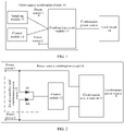
- FIG. 1 shows a power source combination circuit 10 according to an embodiment of this application.
- the power source combination circuit 10 is configured to combine two power sources (for example, a power source 1 and a power source 2) into one power source (that is, a combination power source), to supply power to a load circuit 14.
- the power source combination circuit 10 includes a combination circuit module 11, a control module 12, and a sampling module 13.
- the combination circuit module 11 is configured to provide the combination circuit of two power sources.
- the control module 12 is configured to diagnose the combination circuit module 11 when the power source combination circuit system is powered on. In addition, when the diagnosis result is normal, the combination circuit module 11 is controlled to provide a dual power source to supply power to the load circuit.
- the control module 12 may implement a function of the control module 12 via a micro controller unit (MCU), or may implement a function of the control module 12 through an ECU that has a specific function. This is not limited.
- the sampling module 13 is configured to collect an input side voltage of the combination circuit module 11 and an input voltage of the load circuit, so that the control module 12 may diagnose the combination circuit module 11 based on the collected voltages.
- sampling module 13 and the control module 12 may exist independently, or may be integrated together. This is not limited. For a brief description, an example where the control module 12 and the sampling module 13 are integrated is used for description in this embodiment of this application. It may be understood that the control module 12 described below includes the sampling module 13.
- the control module 12 needs to be powered independently to ensure that the control module 12 works properly.
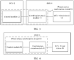
- the dual combination power source 15 controlled by the diodes (for example, a D1 and a D2) shown in FIG. 2 is generally configured to supply power to the control module 12.
- a power source 1 is connected to the diode D1
- a power source 2 is connected to the diode D2.
- Both D1 and D2 are connected to a power source input end of the control module 12, so that the dual combination power source is provided to supply power to the control module 12.
- the power source 1 and the power source 2 shown in FIG. 2 are respectively the power source 1 and the power source 2 connected to the combination circuit module 11 in FIG. 1 .
- the dual combination power source 15 controlled by the diodes fails to bear a low-voltage (for example, a voltage lower than 48 V (volt)) load circuit with relatively high power (for example, power higher than 100 W (watt)).
- a low-voltage for example, a voltage lower than 48 V (volt)
- relatively high power for example, power higher than 100 W (watt)
- an MCU or an ECU that implements a function of the control module 12 is generally an MCU or an ECU with relatively low power.
- the ECU may be the VCU.
- the power source combination circuit 10 provided in this embodiment of this application shown in FIG. 1 may provide a dual power source to supply power to the low-voltage load circuit with relatively high power. For details, refer to the following description. Details are not described herein again.
- An embodiment of this application further provides a power source combination circuit system.
- the power source combination circuit 10 may be used in the power source combination circuit system.
- the power source combination circuit system further includes a load circuit 14.
- the power source combination circuit 10 is configured to provide a dual power source to supply power to the load circuit.
- the power source combination circuit 10 may be used as an independent electronic unit to supply power to any load circuit 14 via a dual power source.
- the load circuit 14 may be an ECU with any foregoing function in an electric vehicle.
- the control module 12 in the power source combination circuit 10 may be an independent MCU.
- the combination circuit module 11 and the control module 12 in the power source combination circuit 10 may be separately integrated into different circuit systems, and provide a dual power source to supply power to the circuit system that integrates the combination circuit module 11.
- the different circuit systems may be different ECUs.
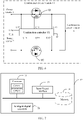
- the combination circuit module 11 may be integrated into an ECU 1
- the control module 12 may be integrated into an ECU 2.
- the control module 12 in the ECU 2 controls the combination circuit module 11 in the ECU 1, thereby providing a dual power source for a load circuit (corresponding to the load circuit 14) of the ECU 1.
- the ECU 1 may be the ADAS
- the ECU 2 may be the VCU. This is not limited herein.
- the combination circuit module 11 and the control module 12 in the power source combination circuit 10 may alternatively be integrated into a same circuit system, and provide a dual power source to supply power to the circuit system.
- the circuit system may be an ECU.
- both the combination circuit module 11 and the control module 12 may be integrated into an ECU 3, and serve as a power source circuit of a load circuit (corresponding to the load circuit 14) of the ECU 3 to provide a dual power source for the load circuit.
- the control module 12 may implement a function of the control module 12 through an MCU integrated into the ECU 3.
- FIG. 5 shows a combination circuit module 11 according to an embodiment of this application.
- the combination circuit module 11 includes a field-effect transistor Q1, a combination controller U1, a field-effect transistor Q2, and a combination controller U2. Both the Q1 and the Q2 are N-channel field-effect transistors.
- the Q1 corresponds to the combination controller U1
- the Q2 corresponds to the combination controller U2.
- the Q1 includes an on state and a cut-off state.
- the internal resistance of the Q1 is very small (for example, at a milliohm level). In this way, even if a current passing through the Q1 is relatively large, the Q1 may not generate excessive heat. In this way, a load circuit connected to the Q1 may be a low-voltage load circuit with high power.
- the Q2 also includes an on state and a cut-off state. For related descriptions of the Q2, refer to the descriptions of the Q1. Details are not described again.
- both the Q1 and the Q2 in the power source combination circuit 10 may be P-channel field-effect transistors.
- one of the Q1 and the Q2 is an N-channel field-effect transistor, and the other is a P-channel field-effect transistor. This is not limited in this embodiment of this application. In FIG. 5 , only an example where both the Q1 and the Q2 are N-channel field-effect transistors is used for description.
- a first end Q11 (corresponding to an excitation end of a first field-effect transistor in this embodiment of this application) of the Q1 may be connected to an excitation port U11 of the combination controller U1.
- the combination controller U1 When an enable end U14 of the combination controller U1 is activated, the combination controller U1 is in a working state.
- the combination controller U1 may input a first excitation voltage to the first end Q11 of the Q1 by using the excitation port U11, to excite the Q1 to be in an on state.
- the enable end U14 of the combination controller U1 is turned off, the combination controller U1 is in a non-working state. In this case, the Q1 is in a cut-off state.
- the first end Q11 of the Q1 may be a gate electrode, and a voltage value of the first excitation voltage needs to be greater than or equal to a critical voltage value that enables the Q1 to be in an on state.
- the enable end U14 of the combination controller U1 may be activated or turned off through a control signal sent by the control module 12. For detailed descriptions, refer to the following descriptions of the control module 12. Details are not described herein again.
- a first end Q21 of the Q2 (corresponding to an excitation end of a second field-effect transistor in this embodiment of this application) may be connected to an excitation port U21 of the combination controller U2.
- the combination controller U2 When an enable end U24 of the combination controller U2 is activated, the combination controller U2 is in a working state. In this case, the combination controller U2 may input a second excitation voltage to the first end Q21 of the Q2 through the excitation port U21, to excite the Q2 to be in an on state.
- the enable end U24 of the combination controller U2 is turned off, the combination controller U2 is in a non-working state. In this case, the Q2 is in a cut-off state.
- the first end Q21 of the Q2 may be a gate electrode, and a voltage value of the second excitation voltage needs to be greater than or equal to a critical voltage value that enables the Q2 to be in an on state.
- the enable end U24 of the combination controller U2 may be activated or turned off through a control signal sent by the control module 12. For detailed descriptions, refer to the following descriptions of the control module 12. Details are not described herein again.
- a second end Q12 (corresponding to an input end of the first field-effect transistor in this embodiment of this application) of the Q1 may be connected to a power source 1, and the second end Q12 of the Q1 may be a source electrode. It may be understood that a voltage stabilizer, a fuse, or another component (not shown in FIG. 5 ) may be further included between the second end Q12 of the Q1 and the power source 1.
- a second end Q22 (corresponding to an input end of the second field-effect transistor in this embodiment of this application) of the Q2 may be connected to a power source 2, and the second end Q22 of the Q2 may be a source electrode. It may be understood that a voltage stabilizer, a fuse, or another component (not shown in FIG. 5 ) may be further included between the second end Q22 of the Q2 and the power source 2.
- both the Q1 and the Q2 are P-channel field-effect transistors
- both the second end Q12 of the Q1 and the second end Q22 of the Q2 may be a drain.
- a drain of the Q1 is connected to the power source 1
- a drain of the Q2 is connected to the power source 2.
- the second end Q12 of the Q1 may further be connected to a port U12 of the combination controller U1. That is, the power source 1 is connected to the port U12 of the combination controller U1. In this way, the power source 1 may be used as a power source of the combination controller U1, so that the combination controller U1 is in a power-on standby state.
- the combination controller U1 may further collect a first input voltage at the second end Q12 of the Q1 by using the port U12. The first input voltage is an input side voltage of the Q1.
- a third end Q13 (corresponding to an output end of the first field-effect transistor in this embodiment of this application) of the Q1 may be connected to a port U13 of the combination controller U1.
- the combination controller U1 may collect a first output voltage at the third end Q13 of the Q1 through the port U13.
- the first output voltage is an output side voltage of the Q1.
- the combination controller U1 controls a voltage output by the excitation port U11 to be lower than the first excitation voltage.
- the combination controller U1 controls the excitation port U11 to stop outputting a voltage, so that the Q1 is in a cut-off state. In this way, a current is prevented from flowing back to the power source 1.
- the second end Q22 of the Q2 may further be connected to a port U22 of the combination controller U2. That is, the power source 2 is connected to the port U22 of the combination controller U2. In this way, the power source 2 may be used as a power source of the combination controller U2, so that the combination controller U2 is in a power-on standby state.
- the combination controller U2 may further collect a second input voltage of the second end Q22 of the Q2 by using the port U22.
- the second input voltage is an input side voltage of the Q2.
- a third end Q23 (corresponding to an output end of the second field-effect transistor in this embodiment of this application) of the Q2 may be connected to a port U23 of the combination controller U2.
- the combination controller U2 may collect a second output voltage of the third end Q23 of the Q2 through the port U23.
- the second output voltage is an output side voltage of the Q2.
- the combination controller U2 controls a voltage output by the excitation port U21 to be lower than the second excitation voltage.
- the combination controller U2 controls the excitation port U21 to stop outputting a voltage, so that the Q2 is in a cut-off state. In this way, a current is prevented from flowing back to the power source 2.
- both a third end Q13 of the Q1 and the third end Q23 of the Q2 may be connected to a load circuit (not shown in FIG. 5 ), so as to serve as a combined power source to supply power to the load circuit.
- Both the third end Q13 of the Q1 and the third end Q23 of the Q2 are drains.
- both the third end Q13 of the Q1 and the third end Q23 of the Q2 may be source electrodes. That is, a source electrode of the Q1 and a source electrode of the Q2 are separately connected to the load circuit, so as to serve as a combined power source to supply power to the load circuit.
- the third end Q13 of the Q1 is a drain.
- the Q2 is a P-channel field-effect transistor, the third end Q23 of the Q2 is a source electrode.
- a drain of the Q1 and a source electrode of the Q2 are separately connected to the load circuit, so as to serve as a combined power source to supply power to the load circuit.
- the third end Q13 of the Q1 is a source electrode.
- the Q2 is an N-channel field-effect transistor, the third end Q23 of the Q2 is a drain.
- a source electrode of the Q1 and a drain of the Q2 are separately connected to the load circuit, so as to serve as a combined power source to supply power to the load circuit.
- a field-effect transistor for example, the Q1 or the Q2 in a power source combination circuit, it needs to be ensured that a positive electrode (D shown in FIG. 5 ) of an internal body diode of the field-effect transistor is connected to a power source. That is, it is ensured that when a field-effect transistor is in an on state, a flow direction of a current in the field-effect transistor is from a positive electrode to a negative electrode of an internal body diode D.
- FIG. 6 shows another combination circuit module 11 according to an embodiment of this application.
- a difference from the combination circuit module shown in FIG. 5 lies in that only one combination controller is configured in FIG. 6 .
- Both the Q1 and the Q2 in the combination circuit module 11 are N-channel field-effect transistors.
- the Q1 and the Q2 share one combination controller U1.
- a power source 1, and the combination controller U1 For interconnections between the Q1, a power source 1, and the combination controller U1, reference may be made to the description of the interconnections between the Q1, the power source 1, and the combination controller U1 in the combination circuit module 11 in FIG. 5 .
- a power source 2, and the combination controller U1 reference may be made to the description of the interconnections between the Q2, the power source 2, and the combination controller U2 in the combination circuit module 11 in FIG. 5 . Details are not described herein.
- an excitation port U11, a port U12, a port U13, and an enable end U14 that are in the combination controller U1 and that are connected to the Q1 are used as a first port group, to control the Q1 to be in an on state or a cut-off state.
- An excitation port U15, a port U16, a port U17, and an enable end U18 that are in the combination controller U1 and that are connected to the Q2 are used as a second port group, to control the Q2 to be in an on state or a cut-off state.
- FIG. 7 is a schematic structural diagram of a control module 12 according to an embodiment of this application.
- the control module 12 includes the sampling module 13 is used for description.
- the control module 12 is configured to control a combination circuit module 11 to provide a dual power source to supply power to a load circuit.
- the control module 12 may be an MCU or an ECU. This is not limited herein.
- the control module 12 may include a processor 71, an analog-to-digital converter (analog-to-digital converter, ADC) 72 (corresponding to the sampling module in this embodiment of this application), and an input/output interface 73.
- the control module 12 may further be a memory 74.
- the ADC 72 (equivalent to the sampling module in this embodiment of this application), the input/output interface 73, and the memory 74 may be separately connected to and communicate with the processor 71.
- the processor 71 is a control center of the control module 12. It may be a general-purpose central processing unit (central processing unit, CPU), or may be another general-purpose processor, a digital signal processor (digital signal processing, DSP), an application-specific integrated circuit (application-specific integrated circuit, ASIC), a field-programmable gate array (field-programmable gate array, FPGA), or another programmable logic component, a discrete gate or a transistor logic device, a discrete hardware component, or the like.
- the general-purpose processor may be a microprocessor, any conventional processor, or the like.
- the processor 71 may include one or more CPUs, for example, a CPU 0 and a CPU 1 shown in FIG. 7 .
- the ADC 72 is configured to collect a first input voltage of a Q1, a second input voltage of a Q2, and a third input voltage of a load circuit in a combination circuit module 11.
- the ADC 72 further sends the first input voltage, the second input voltage, and the third input voltage that are collected to the processor 71 for diagnostic analysis.
- the first input voltage is an input side voltage of the Q1
- the second input voltage is an input side voltage of the Q2
- the third input voltage is an input voltage of the load circuit. That is, the third input voltage is a voltage at a power source input end of the load circuit.
- a quantity of the ADC 72 is related to a quantity of power sources that need to be combined by the combination circuit module 11. If the quantity of power sources that need to be combined by the combination circuit module 11 is m, the quantity of the ADC 72 is m+1.
- m is an integer greater than or equal to 1.
- a combination circuit module 11 includes two power sources (a power source 1 and a power source 2) that need to be combined. Therefore, the control module 12 may include three ADCs 72 (an ADC 72_1, an ADC 72_2, and an ADC 72_3).
- the ADC 72_1 may be connected to a second end Q12 of the Q1 through a port 121. It collects a first input voltage VA at the second end Q12 of the Q1.
- the ADC 72_2 may be connected to a second end Q22 of the Q2 through a port 122. It collects a second input voltage VB at the second end Q22 of the Q2.
- the ADC 72_3 may be connected to a power source input end 141 of a load circuit 14 through a port 123. It collects a third input voltage VC of the power source input end 141 of the load circuit 14.
- An input/output interface 73 may be a general-purpose input/output interface (general-purpose input/output, GPIO).
- the input/output interface 73 is configured to send a control signal to the combination circuit module 11, so as to activate or turn off an enable end of a combination controller in the combination circuit module 11. Further, when the enable end of the combination controller in the combination circuit module 11 is activated, the combination controller is in a working state. In this way, the combination controller may input an excitation voltage to a field-effect transistor through an excitation port, so that the field-effect transistor is in an on state. Alternatively, when the enable end of the combination controller in the combination circuit module 11 is turned off, the combination controller is in a non-working state. In this way, the field-effect transistor cannot receive an excitation voltage that is input by the combination controller through an excitation port. That is, the field-effect transistor is in a cut-off state.
- the control signal may be a level signal.
- the control signal may include at least one level signal of a high level signal or a low level signal.
- the input/output interface 73 may send a high level signal to the enable end of the combination controller to activate the combination controller.
- the input/output interface 73 may send a low level signal to the enable end of the combination controller to turn off the combination controller.
- the input/output interface 73 may send a low level signal to the enable end of the combination controller to activate the combination controller.
- the input/output interface 73 may send a high level signal to the enable end of the combination controller to turn off the combination controller. This is not limited in this embodiment of this application.
- a quantity of the input/output interfaces 73 is the same as the quantity of power sources that need to be combined by the combination circuit module 11. If the quantity of power sources that need to be combined by the combination circuit module 11 is m, the quantity of the input/output interfaces 73 is m.
- the combination circuit module 11 includes the two power sources (the power source 1 and the power source 2) that need to be combined. Therefore, the control module 12 may include two input/output interfaces 73 (a port 124 and a port 125).
- the port 124 of the control module 12 is connected to an enable end U14 of a combination controller U1.
- the port 124 may send a control signal to the enable end U14 of the combination controller U1.
- the control signal may be used to activate the combination controller U1, so that the Q1 is in an on state.
- the control signal may be used to turn off the combination controller U1, so that the Q1 is in a cut-off state.
- the control signal may include at least one signal of a high level signal or a low level signal. This is not limited.
- the port 125 of the control module 12 is connected to an enable end U24 of a combination controller U2. According to an instruction of the processor 71, the port 125 may send a control signal to the enable end U24 of the combination controller U2.
- the control signal may be used to activate the combination controller U2, so that the Q2 is in an on state.
- the control signal may be used to turn off the combination controller U2, so that the Q2 is in a cut-off state.
- the ADC 72 and the input/output interface 73 may be integrated with the processor 71.
- a component integrating the ADC 72, the input/output interface 73, and the processor 71 may be referred to as an MCU.
- the memory 74 may be a read-only memory (read-only memory, ROM) or another type of static storage device capable of storing static information and instructions, a random access memory (random access memory, RAM) or another type of dynamic storage device capable of storing information and instructions, an electrically erasable programmable read-only memory (electrically erasable programmable read-only memory, EEPROM), a magnetic disk storage medium or another magnetic storage device, or any other medium capable of carrying or storing expected program code in a form of an instruction or data structure and capable of being accessed by a computer, but is not limited thereto.
- ROM read-only memory
- RAM random access memory
- EEPROM electrically erasable programmable read-only memory
- magnetic disk storage medium or another magnetic storage device or any other medium capable of carrying or storing expected program code in a form of an instruction or data structure and capable of being accessed by a computer, but is not limited thereto.
- the memory 74 may be independent of the processor 71.
- the memory 74 may be connected to the processor 71 through a bus, and is configured to store data, instructions, or program code.
- the processor 71 invokes and executes the instructions or the program code stored in the memory 74, the processor 71 may implement the power source combination circuit diagnosis method provided in this embodiment of this application.
- the memory 74 may alternatively be integrated with the processor 71.
- control module 12 may include more or fewer components than those shown in the figure, or combine some components, or have different component arrangements.
- control module 12 in the power source combination circuit 10 controls conduction of a field-effect transistor in the combination circuit module 11, so as to combine the power source 1 and the power source 2 into one power source and supply power to a load circuit.
- an embodiment of this application further provides a power source combination circuit diagnosis method.
- the diagnosis method is used to diagnose a faulty component in the power source combination circuit 10, and an alarm is sent to a user when a failure is diagnosed.
- FIG. 9 is a schematic flowchart of the power source combination circuit diagnosis method according to an embodiment of this application. The method is applied to the power source combination circuit system shown in FIG. 8 , and the method may include the following steps:
- a control module 12 sends a control signal to a combination circuit module 11, so as to control and obtain a state combination of field-effect transistors in the combination circuit module 11.
- the control module 12 may send a first group of control signals, a second group of control signals, a third group of control signals, and a fourth group of control signals to the combination circuit module 11 through the input/output interface.
- the first group of control signals, the second group of control signals, the third group of control signals, and the fourth group of control signals are respectively four groups of control signals sent by the control module 12 to the combination circuit module 11 at different moments.
- each group of control signals in the first group of control signals, the second group of control signals, the third group of control signals, and the fourth group of control signals includes a first signal and a second signal. The first signal is used to control an enable end of the combination controller U1 in the combination circuit module 11, and the second signal is used to control an enable end of the combination controller U2 in the combination circuit module 11.
- the first signal in the first group of control signals may be used to activate the enable end of the combination controller U1 in the combination circuit module 11, so that the combination controller U1 is in a working state.
- the second signal in the first group of control signals may be used to activate the enable end of the combination controller U2, so that the combination controller U2 is in a working state.
- the combination controller U1 may control the Q1 to be in an on state
- the combination controller U2 may control the Q2 to be in an on state.
- the first signal in the second group of control signals may be used to activate the enable end of the combination controller U1 in the combination circuit module 11, so that the combination controller U1 is in a working state.
- the second signal in the second group of control signals may be used to turn off the enable end of the combination controller U2 in the combination circuit module 11, so that the combination controller U2 is in a non-working state.
- the combination controller U1 may control the Q1 to be in an on state, and the combination controller U2 may control the Q2 to be in a cut-off state.
- the first signal in the third group of control signals may be used to activate the enable end of the combination controller U2 in the combination circuit module 11, so that the combination controller U2 is in a working state.
- the second signal in the third group of control signals may be used to turn off the enable end of the combination controller U1 in the combination circuit module 11, so that the combination controller U1 is in a non-working state.
- the combination controller U2 may control the Q2 to be in an on state
- the combination controller U1 may control the Q1 to be in a cut-off state.
- the first signal in the fourth group of control signals may be used to turn off the enable end of the combination controller U1 in the combination circuit module 11, so that the combination controller U1 is in a non-working state.
- the second signal in the fourth group of control signals may be used to turn off the enable end of the combination controller U2 in the combination circuit module 11, so that the combination controller U2 is in a non-working state.
- the combination controller U1 may control the Q1 to be in a cut-off state
- the combination controller U2 may control the Q2 to be in a cut-off state.
- the first group of control signals may control and obtain a first state combination of the field-effect transistors in the combination circuit module 11: Both the Q1 and the Q2 are in an on state.
- the second group of control signals may control and obtain a second state combination of the field-effect transistors in the combination circuit module 11: The Q1 is in an on state and the Q2 is in a cut-off state.
- the third group of control signals may control and obtain a third state combination of the field-effect transistors in the combination circuit module 11: The Q1 is in a cut-off state and the Q2 is in an on state.
- the fourth group of control signals may control and obtain a fourth state combination of the field-effect transistors in the combination circuit module 11: Both the Q1 and the Q2 are in a cut-off state.
- a time sequence is not limited in embodiments of this application for the control module 12 to send the first group of control signals, the second group of control signals, the third group of control signals, and the fourth group of control signals to the combination circuit module 11.
- the control module 12 may send the first group of control signals, the second group of control signals, the third group of control signals, and the fourth group of control signals to the combination circuit module 11 in sequence.
- the control module 12 may send the second group of control signals first, and then send the first group of control signals, the third group of control signals, the fourth group of control signals in sequence, or in similar ways.
- a time sequence for the control module 12 to control and obtain a state combination of the field-effect transistors in the combination circuit module 11 is not limited.
- the control module 12 may control and obtain the first state combination, the second state combination, the third state combination, and the fourth state combination of the field-effect transistors in the combination circuit module 11 in sequence.
- the control module 12 may alternatively control and obtain the second state combination of the field-effect transistors in the combination circuit module 11 first, and then control and obtain the third state combination, the first state combination, and the fourth state combination in sequence. This is not limited herein.
- statuses of the field-effect transistors in the combination circuit module 11 may be the first state combination, the second state combination, the third state combination, and the fourth state combination respectively.
- the control module 12 obtains a first input voltage, a second input voltage, and a third input voltage of the field-effects transistor that are in the combination circuit module 11 and that are in different state combinations.
- control module 12 may collect the first input voltage, the second input voltage, and the third input voltage of the field-effect transistors that are in the combination circuit module 11 and that are in the different state combinations by using a sampling module, so as to obtain the first input voltage, the second input voltage, and the third input voltage of the field-effect transistors that are in the combination circuit module 11 and that are in the different state combinations.
- the sampling module collects the first input voltage, the second input voltage, and the third input voltage of the field-effect transistors that are in the combination circuit module 11 and that are in different state combinations, and sends the collected voltages to the control module 12.
- the control module 12 obtains the first input voltage, the second input voltage, and the third input voltage of the field-effect transistors that are in the combination circuit module 11 and that are in the different state combinations.
- the first input voltage may be an input side voltage VA of the Q1
- the second input voltage may be an input side voltage VB of the Q2
- the third input voltage may be an input voltage VC of the load circuit.
- control module 12 may respectively collect, by using ADCs, a first input voltage VA1, a second input voltage VB 1, and a third input voltage VC 1 when the state combination of the field-effect transistors in the combination circuit module 11 is the first state combination.
- the control module 12 may respectively collect, by using the ADCs, a first input voltage VA2, a second input voltage VB2, and a third input voltage VC2 when the state combination of the field-effect transistors in the combination circuit module 11 is the second state combination.
- the control module 12 may respectively collect, by using the ADCs, a first input voltage VA3, a second input voltage VB3, and a third input voltage VC3 when the state combination of the field-effect transistors in the combination circuit module 11 is the third state combination.
- the control module 12 may be controlled to respectively collect, by using the ADCs, a first input voltage VA4, a second input voltage VB4, and a third input voltage VC4 when the state combination of the field-effect transistors in the combination circuit module 11 is the fourth state combination.
- the control module 12 diagnoses the combination circuit module 11 based on the first input voltage, the second input voltage, the third input voltage, and a preset parameter of the field-effect transistors that are in the combination circuit module 11 and that are in the different state combinations.
- the preset parameter may include the following values: a minimum forward voltage drop of an internal body diode of the Q1 (VQ1_D_min), a maximum forward voltage drop of the internal body diode of the Q1 (VQ1_D_max), a minimum forward voltage drop of an internal body diode of the Q2 (VQ2_D_min), and a maximum forward voltage drop of the internal body diode of the Q2 (VQ2 _D _max), a maximum voltage difference that is calculated on the basis of a maximum current of the load circuit and a maximum conductive internal direct current resistance of the Q1 and that flows through the Q1 (VQ1_max), and a maximum voltage difference that is calculated on the basis of the maximum current of the load circuit and a maximum conductive internal direct current resistance of the Q2 and that is of the Q2 (VQ2_max).
- control module may diagnose the combination circuit module 11 according to the diagnosis criteria shown in Table 1, and obtain a corresponding diagnosis result.
- Table 1 The State combination of the Field-Effect Transistors in the Combination Circuit Module 11 Diagnosis Criteria Diagnosis Result
- the combination circuit module 11 is normal.
- the combination circuit module 11 is abnormal.
- the second state combination When VA2 ⁇ (VB2 - (VQ2_D_max)), (VB2 - VQ2_D_max) ⁇ VC2 ⁇ (VB2 - VQ2_D_min)
- the combination circuit module 11 is normal.
- VC2 ⁇ (VA2 - VQ1_max) The combination circuit module 11 is normal.
- VA2 ⁇ ((VB2 - VQ2_D_min) + VQ1_max)
- VC2 ⁇ VA2 - VQ1_max
- the Q1 is abnormal, or the U1 is abnormal.
- the third state combination When VB3 ⁇ (VA3 - (VQ1_D_max)), (VA3 - VQ1_D_max) ⁇ VC3 ⁇ (VA3 - VQ1_D_min)
- the combination circuit module 11 is normal.
- VC3 ⁇ VA3 - VQ1_D_max
- the Q1 is abnormal.
- the VC1 When a state combination of the field-effect transistors in the combination circuit module 11 is the first state combination, that is, both the Q1 and the Q2 are in an on state, the VC1 satisfies the following conditions at the same time: greater than or equal to (VA1 - VQ1_max), and greater than or equal to (VB1 - VQ2_max). That is, when the VC1 is greater than or equal to the larger one of (VA1 - VQ1_max) and (VB1 - VQ2_max), it indicates that the combination circuit module 11 is normal. Otherwise, it indicates that the combination circuit module 11 is abnormal.
- a state combination of the field-effect transistors in the combination circuit module 11 is the second state combination, that is, the Q1 is in an on state and the Q2 is in a cut-off state, because a conductive internal resistance is very small, a voltage difference generated by the internal resistance of the Q1 is far less than a voltage drop generated by a body diode inside the Q2.
- VA2 When the VA2 is greater than or equal to ((VB2 - VQ2_D_min) + VQ1_max), if the VC2 is greater than or equal to (VA2 - VQ1_max), it indicates that the combination circuit module 11 is normal; otherwise, it indicates that the Q1 or the U1 is abnormal, for example, a conductive impedance of the Q1 is excessively large, or an excitation voltage output by an excitation end of the U1 is lower than the first excitation voltage.
- a state combination of the field-effect transistors in the combination circuit module 11 is the third state combination, that is, the Q1 is in a cut-off state and the Q2 is in an on state, because a conductive internal resistance of the Q2 is very small, a voltage difference generated by the internal resistance of the Q2 is far less than a voltage drop generated by a body diode inside the Q1.
- the VB3 is greater than or equal to ((VA3 - VQ1_D_min) + VQ2_max)
- the VC is greater than or equal to (VB3 - VQ2_max)
- the VC4 When a state combination of the field-effect transistors in the combination circuit module 11 is the fourth state combination, that is, both the Q1 and the Q2 are in a cut-off state, the VC4 may be within a normal voltage drop range of body diodes inside the Q1 and the Q2. Therefore, when the VC4 is between (VA4 - VQ1_D_max) and (VA4 - VQ1_D_min), or, when the VC4 is between (VB4 - VQ2_D_max) and (VB4 - VQ2_D_min), it indicates that the combination circuit module 11 is normal. Otherwise, it indicates that the combination circuit module 11 is abnormal.
- the four state combinations of the field-effect transistors in the combination circuit module 11 are referred to as “the four state combinations" for short.
- the control module 12 diagnoses the combination circuit module 11. If the diagnosis result is normal, it indicates that the combination circuit module 11 is normal. In this case, the control module 12 may continuously control both the Q1 and the Q2 to be in an on state, so as to supply power to the load circuit normally. When a diagnosis result of at least one state combination among the four state combinations is abnormal, the control module 12 may control both the Q1 and the Q2 to be in a cut-off state, and send alarm information to a user interaction module to remind a user that the power source combination circuit system is abnormal.
- control module 12 diagnoses the combination circuit module 11 based on the first input voltages, the second input voltages, and the third input voltages that are collected in the four state combinations.
- the four state combinations are state combinations of the field-effect transistors in the combination circuit module 11 at different moments. Therefore, when the control module 12 may control and obtain one state combination of the field-effect transistors in the combination circuit module 11, that is, based on a first input voltage, a second input voltage, and a third input voltage that are collected in this state combination, the control module 12 may perform a diagnosis on the combination circuit module 11 and obtain a diagnosis result. In this way, the control module may perform four diagnoses based on a first input voltage, a second input voltage, and a third input voltage that are collected each time, to obtain four diagnosis results. Then, the control module 12 determines whether the combination circuit module 11 is normal based on the four diagnosis results.
- the control module 12 may stop diagnosing the combination circuit module 11, control both the Q1 and the Q2 to be in a cut-off state, and send alarm information to the user interaction module to remind a user that the power source combination circuit system is abnormal.
- the diagnosis result prompting "abnormal" is not a diagnosis result of the fourth diagnosis, the quantity of times of collecting a first input voltage, a second input voltage, and a third input voltage of the combination circuit module 11 by the control module 12 is reduced, and the quantity of times of diagnosing the combination circuit module 11 is reduced, thereby improving efficiency of the power source combination circuit diagnosis method provided in the embodiments of this application.
- control module 12 may alternatively first collect the first input voltages, the second input voltages, and the third input voltages in the four state combinations, and then diagnose the combination circuit module 11 according to the criteria in Table 1 to determine whether the combination circuit module 11 is normal.
- the control module 12 detects a first input voltage, a second input voltage, and a third input voltage in different state combinations of the Q1 corresponding to a first power source and the Q2 corresponding to a second power source, and determines whether values of the first input voltage, the second input voltage, and the third input voltage are within a theoretical range in each state combination, so as to diagnose a failure of a component in the combination circuit module 11.
- the embodiments of this application provide a power source combination circuit diagnosis method that may be used to diagnose a power source combination circuit before the power source combination circuit supplies power to a load circuit.
- a component in the power source combination circuit is diagnosed as abnormal, power supply to the load circuit may be stopped. By doing so, it is ensured that no faults occur in the load circuit during a power supply process due to the abnormality of the power source combination circuit, thereby improving security of the load circuit.
- the embodiments of this application further provide a power source combination circuit and a system.
- the power source combination circuit uses a field-effect transistor as a key component.
- the power source combination circuit may supply power to two or more power sources for a low-voltage load circuit with relatively high power.
- the power source combination circuit diagnosis apparatus may be divided into function modules based on the foregoing method examples.
- each function module may be obtained through division based on each corresponding function, or two or more functions may be integrated into one processing module.
- the integrated module may be implemented in a form of hardware, or may be implemented in a form of a software functional module. It should be noted that in embodiments of this application, division into the modules is an example and is merely logical function division, and may be other division in an actual implementation.
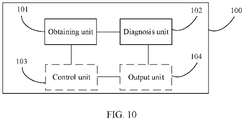
- FIG. 10 is a schematic structural diagram of a power source combination circuit diagnosis apparatus 100 according to an embodiment of this application.
- the diagnosis apparatus 100 is used in a power source combination circuit in a power source combination circuit system, and the power source combination circuit further includes a combination circuit module.
- the combination circuit module contains a first power source, a first field-effect transistor, a second power source, and a second field-effect transistor.
- the first power source is connected to an input end of the first field-effect transistor
- the second power source is connected to an input end of the second field-effect transistor
- both an output end of the first field-effect transistor and an output end of the second field-effect transistor are connected to a power source port of a load circuit.
- the diagnosis apparatus 100 is configured to control the combination circuit module to supply power to the load circuit.
- the diagnosing apparatus 100 is configured to diagnose the power source combination circuit.
- the diagnosing apparatus 100 is further used to perform the foregoing power source combination circuit diagnosis method, for example, it is used to perform the method shown in FIG. 9 .
- the diagnosis apparatus 100 may include an obtaining unit 101 and a diagnosis unit 102.
- the obtaining unit 101 is configured to obtain a first input voltage, a second input voltage, and a third input voltage.
- the first input voltage is an input side voltage of the first field-effect transistor
- the second input voltage is an input side voltage of the second field-effect transistor
- the third input voltage is a voltage at a power source end of the load circuit.
- the diagnosis unit 102 is configured to diagnose, based on the obtained voltages, whether the combination circuit module is abnormal.
- the obtaining unit 101 may be used to perform the S102, and the diagnosis unit 102 may be used to perform the S103.
- the diagnosis unit 102 is specifically configured to diagnose, based on the obtained voltage and a preset parameter, whether the combination circuit module is abnormal.
- the preset parameter includes at least one of the following values: a minimum forward voltage drop value of an internal body diode of the first field-effect transistor, a maximum forward voltage drop value of the internal body diode of the first field-effect transistor, a minimum forward voltage drop value of an internal body diode of the second field-effect transistor, a maximum forward voltage drop value of the internal body diode of the second field-effect transistor, a maximum voltage difference value that is calculated on the basis of a maximum current of the load circuit and that is of the first field-effect transistor, or a maximum voltage difference value that is calculated on the basis of the maximum current of the load circuit and that is of the second field-effect transistor.
- the diagnosis unit 102 may be used to perform the S103.
- the power source combination circuit further includes a sampling module.
- the sampling module is connected to the input end of the first field-effect transistor, the input end of the second field-effect transistor, and a power source input end of the load circuit.
- the sampling module is configured to collect the first input voltage, the second input voltage, and the third input voltage.
- the obtaining unit 101 is specifically configured to obtain the first input voltage, the second input voltage, and the third input voltage that are collected by the sampling module.
- the obtaining unit 101 may be configured to perform the S102.
- the diagnosis apparatus 100 further includes: a control unit 103 that is configured to control statuses of the first field-effect transistor and the second field-effect transistor.
- the statuses include an on state and a cut-off state.
- the obtaining unit 101 is specifically configured to obtain a first input voltage, a second input voltage, and a third input voltage when the first field-effect transistor and the second field-effect transistor are in a target state combination and that are collected by the sampling module.
- the target state combination includes any one of the following combinations: both the first field-effect transistor and the second field-effect transistor are in an on state; both the first field-effect transistor and the second field-effect transistor are in a cut-off state; the first field-effect transistor is in an on state, and the second field-effect transistor is in a cut-off state; and the first field-effect transistor is in a cut-off state, and the second field-effect transistor is in an on state.
- control unit 103 may be configured to perform the S101, and the obtaining unit 101 may be configured to perform the S102.
- the combination circuit module further includes a first combination controller and a second combination controller.
- the first combination controller is connected to an excitation end of the first field-effect transistor
- the second combination controller is connected to an excitation end of the second field-effect transistor.
- the control unit 103 is specifically configured to control the first combination controller to output a first excitation voltage.
- the first excitation voltage is used to control the first field-effect transistor to be in an on state.
- the control unit 103 is further configured to control the second combination controller to output a second excitation voltage.
- the second excitation voltage is used to control the second field-effect transistor to be in an on state.
- control unit 103 may be configured to perform the S101.
- control unit 103 is further configured to control both the first field-effect transistor and the second field-effect transistor to be in an on state, so as to control the combination circuit module to supply power to the load circuit.
- the diagnosis apparatus 100 further includes: an output unit 104 that is configured to output an alarm signal if the diagnosis result of the combination circuit module is abnormal.
- power of the diagnosis apparatus 100 is less than or equal to a preset threshold, and power of the load circuit is greater than or equal to the preset threshold.
- functions implemented by the obtaining unit 101, the diagnosis unit 102, and the control unit 103 in the diagnosis apparatus 100 may be implemented by the processor 71 in FIG. 7 by executing the program instruction in the memory 74.
- a function implemented by an output unit 104 may be implemented by using the input/output interface 73 in FIG. 7 .
- Another embodiment of this application further provides a computer-readable storage medium.
- the computer-readable storage medium stores an instruction.
- the instruction runs on a power source combination circuit diagnosis apparatus
- the power source combination circuit diagnosis apparatus performs the steps performed by the power source combination circuit diagnosis apparatus in the method procedure shown in the foregoing method embodiment.
- the disclosed method may be implemented as computer program instructions encoded in a machine-readable format on a computer-readable storage medium or encoded on another non-transitory medium or product.
- An embodiment of this application further provides a proper power source circuit system.
- the system includes the power source combination circuit shown in FIG. 1 or FIG. 2 .
- the power source combination circuit is used to implement the foregoing diagnosis method of the power source combination diagnosis apparatus. For brevity, details are not described herein again.
- All or some of the foregoing embodiments may be implemented by using software, hardware, firmware, or any combination thereof.
- a software program is used to implement the embodiments, all or a part of the embodiments may be implemented in a form of a computer program product.
- the computer program product includes one or more computer instructions.
- the computer-executable instructions When the computer-executable instructions are loaded and executed on a computer, the procedures or functions according to embodiments of this application are all or partially generated.
- the computer may be a general-purpose computer, a dedicated computer, a computer network, or another programmable apparatus.
- the computer instructions may be stored in a computer-readable storage medium or may be transmitted from a computer-readable storage medium to another computer-readable storage medium.
- the computer instructions may be transmitted from a website, computer, server, or data center to another website, computer, server, or data center in a wired (for example, a coaxial cable, an optical fiber, or a digital subscriber line (digital subscriber line, DSL)) or wireless (for example, infrared, radio, or microwave) manner.
- the computer-readable storage medium may be any usable medium accessible by a computer, or a data storage device, such as a server or a data center, integrating one or more usable media.
- the usable medium may be a magnetic medium (for example, a floppy disk, a hard disk, or a magnetic tape), an optical medium (for example, a DVD), a semiconductor medium (for example, a solid-state drive (solid-state drive, SSD)), or the like.
- a magnetic medium for example, a floppy disk, a hard disk, or a magnetic tape
- an optical medium for example, a DVD
- a semiconductor medium for example, a solid-state drive (solid-state drive, SSD)
Landscapes
- Engineering & Computer Science (AREA)
- Power Engineering (AREA)
- Physics & Mathematics (AREA)
- General Physics & Mathematics (AREA)
- Business, Economics & Management (AREA)
- Emergency Management (AREA)
- General Engineering & Computer Science (AREA)
- Electronic Switches (AREA)
Applications Claiming Priority (2)
| Application Number | Priority Date | Filing Date | Title |
|---|---|---|---|
| CN202010203132.XA CN113497486B (zh) | 2020-03-20 | 2020-03-20 | 电源合路电路、诊断方法、装置及系统 |
| PCT/CN2021/079318 WO2021185099A1 (zh) | 2020-03-20 | 2021-03-05 | 电源合路电路、诊断方法、装置及系统 |
Publications (2)
| Publication Number | Publication Date |
|---|---|
| EP4113784A1 true EP4113784A1 (de) | 2023-01-04 |
| EP4113784A4 EP4113784A4 (de) | 2023-08-23 |
Family
ID=77768336
Family Applications (1)
| Application Number | Title | Priority Date | Filing Date |
|---|---|---|---|
| EP21772345.1A Pending EP4113784A4 (de) | 2020-03-20 | 2021-03-05 | Stromquellenkombinationsschaltung, diagnoseverfahren und -vorrichtung sowie system |
Country Status (4)
| Country | Link |
|---|---|
| US (1) | US12160134B2 (de) |
| EP (1) | EP4113784A4 (de) |
| CN (1) | CN113497486B (de) |
| WO (1) | WO2021185099A1 (de) |
Families Citing this family (3)
| Publication number | Priority date | Publication date | Assignee | Title |
|---|---|---|---|---|
| US11322930B1 (en) * | 2020-10-20 | 2022-05-03 | Lear Corporation | Electrical system including a power distribution circuit |
| CN116169877A (zh) * | 2023-03-03 | 2023-05-26 | 北京全路通信信号研究设计院集团有限公司 | 一种电源电路 |
| CN120237936B (zh) * | 2025-05-30 | 2025-08-26 | 苏州元脑智能科技有限公司 | 合路控制电路及其控制方法、设备、介质以及产品 |
Family Cites Families (11)
| Publication number | Priority date | Publication date | Assignee | Title |
|---|---|---|---|---|
| US7256605B2 (en) * | 2005-11-14 | 2007-08-14 | Semiconductor Components Industries, L.L.C. | Diagnostic circuit and method therefor |
| CN101226414B (zh) * | 2008-01-30 | 2012-01-11 | 北京中星微电子有限公司 | 一种动态补偿基准电压的方法以及带隙基准电压源 |
| JP4978491B2 (ja) * | 2008-02-05 | 2012-07-18 | 日本電気株式会社 | 電源システムおよび素子故障検出方法 |
| CN101728866B (zh) * | 2008-10-21 | 2012-06-13 | 中兴通讯股份有限公司 | 一种实现电源倒换的装置与方法 |
| CN101958576B (zh) * | 2010-05-20 | 2013-03-13 | 福建星网锐捷网络有限公司 | 电源冗余并联电路和工作方法 |
| TWI428613B (zh) * | 2010-08-02 | 2014-03-01 | Acbel Polytech Inc | Abnormal detection method and device for server power supply system |
| CN103219790B (zh) * | 2012-01-20 | 2015-05-13 | 登丰微电子股份有限公司 | 双电源供应系统及双电源控制器 |
| US9766299B2 (en) * | 2015-03-19 | 2017-09-19 | Hamilton Sundstrand Corporation | Method for electronically testing integrity of ideal diode components used in OR'd voltage bus |
| CN106848998B (zh) * | 2017-02-28 | 2019-05-24 | 浙江大华技术股份有限公司 | 一种电源输出保护电路及装置 |
| CN109660364B (zh) * | 2019-01-31 | 2020-08-18 | 普联技术有限公司 | 一种供电系统 |
| CN109787348A (zh) * | 2019-02-18 | 2019-05-21 | 北京星际荣耀空间科技有限公司 | 电源合路电路及电器设备 |
-
2020
- 2020-03-20 CN CN202010203132.XA patent/CN113497486B/zh active Active
-
2021
- 2021-03-05 EP EP21772345.1A patent/EP4113784A4/de active Pending
- 2021-03-05 WO PCT/CN2021/079318 patent/WO2021185099A1/zh not_active Ceased
-
2022
- 2022-09-20 US US17/948,341 patent/US12160134B2/en active Active
Also Published As
| Publication number | Publication date |
|---|---|
| CN113497486A (zh) | 2021-10-12 |
| EP4113784A4 (de) | 2023-08-23 |
| WO2021185099A1 (zh) | 2021-09-23 |
| CN113497486B (zh) | 2024-01-30 |
| US12160134B2 (en) | 2024-12-03 |
| US20230015317A1 (en) | 2023-01-19 |
Similar Documents
| Publication | Publication Date | Title |
|---|---|---|
| US12160134B2 (en) | Power source combination circuit, diagnosis method and apparatus, and system | |
| US8545381B2 (en) | Auxiliary artificial heart pump drive device and auxiliary artificial heart system | |
| US11340297B2 (en) | Relay examination device and battery management system | |
| US20220229479A1 (en) | Power supply unit (psu)-based power supply system | |
| US20230006437A1 (en) | Motor control system and vehicle | |
| CN110936821B (zh) | 汽车电机控制器、控制系统及汽车 | |
| CN107433977B (zh) | 具有看门狗监控功能的电动助力转向系统及其控制方法 | |
| US20150357864A1 (en) | Power source switching apparatus and methods for dual-powered electronic devices | |
| CN104869003A (zh) | 供电设备和方法 | |
| CN211478502U (zh) | 高压互锁检测电路及包含其的车辆 | |
| CN207117578U (zh) | 保护电路 | |
| WO2021253336A1 (zh) | 车载驱动电路、车载驱动芯片、车载驱动器件及电子设备 | |
| CN115360908A (zh) | 一种基于集成电源的舵机管理系统及方法 | |
| KR20170024817A (ko) | 제어라인 진단 장치 | |
| CN105610233B (zh) | 多电源并联供电系统及电源短路保护电路 | |
| CN106340948B (zh) | 一种三电源自动切换电路 | |
| CN107506281A (zh) | 一种多路电源监控系统及方法 | |
| CN112073055B (zh) | 一种可配置安全输入输出电路及其配置方法 | |
| CN104617764B (zh) | 加电顺序控制系统 | |
| CN113978256B (zh) | 一种电动汽车双dcdc的控制方法、装置、设备及存储介质 | |
| US20230261225A1 (en) | Apparatus for Converting Power of Fuel Cell for Power Generation and Method Thereof | |
| CN112858894A (zh) | 接触器工作状态的检测方法、检测装置、存储介质及车辆 | |
| CN120752157A (zh) | 用于对机动车中的至少一个与安全相关的用电器进行能量供应的装置 | |
| CN221233859U (zh) | 电动助力转向系统及其诊断装置、车辆 | |
| CN120879476A (zh) | 一种电机控制器pwm驱动信号故障监测电路 |
Legal Events
| Date | Code | Title | Description |
|---|---|---|---|
| STAA | Information on the status of an ep patent application or granted ep patent |
Free format text: STATUS: THE INTERNATIONAL PUBLICATION HAS BEEN MADE |
|
| PUAI | Public reference made under article 153(3) epc to a published international application that has entered the european phase |
Free format text: ORIGINAL CODE: 0009012 |
|
| STAA | Information on the status of an ep patent application or granted ep patent |
Free format text: STATUS: REQUEST FOR EXAMINATION WAS MADE |
|
| 17P | Request for examination filed |
Effective date: 20220927 |
|
| AK | Designated contracting states |
Kind code of ref document: A1 Designated state(s): AL AT BE BG CH CY CZ DE DK EE ES FI FR GB GR HR HU IE IS IT LI LT LU LV MC MK MT NL NO PL PT RO RS SE SI SK SM TR |
|
| DAV | Request for validation of the european patent (deleted) | ||
| DAX | Request for extension of the european patent (deleted) | ||
| A4 | Supplementary search report drawn up and despatched |
Effective date: 20230720 |
|
| RIC1 | Information provided on ipc code assigned before grant |
Ipc: G01R 31/40 20200101ALI20230714BHEP Ipc: G01R 19/165 20060101ALI20230714BHEP Ipc: H02J 9/06 20060101AFI20230714BHEP |
|
| RAP1 | Party data changed (applicant data changed or rights of an application transferred) |
Owner name: SHENZHEN YINWANG INTELLIGENTTECHNOLOGIES CO., LTD. |