EP4113609B1 - Transistor und anzeigevorrichtung damit - Google Patents
Transistor und anzeigevorrichtung damit Download PDFInfo
- Publication number
- EP4113609B1 EP4113609B1 EP22181385.0A EP22181385A EP4113609B1 EP 4113609 B1 EP4113609 B1 EP 4113609B1 EP 22181385 A EP22181385 A EP 22181385A EP 4113609 B1 EP4113609 B1 EP 4113609B1
- Authority
- EP
- European Patent Office
- Prior art keywords
- electrode
- transistor
- disposed
- connection electrode
- connection
- Prior art date
- Legal status (The legal status is an assumption and is not a legal conclusion. Google has not performed a legal analysis and makes no representation as to the accuracy of the status listed.)
- Active
Links
Images







Classifications
-
- H—ELECTRICITY
- H10—SEMICONDUCTOR DEVICES; ELECTRIC SOLID-STATE DEVICES NOT OTHERWISE PROVIDED FOR
- H10D—INORGANIC ELECTRIC SEMICONDUCTOR DEVICES
- H10D89/00—Aspects of integrated devices not covered by groups H10D84/00 - H10D88/00
- H10D89/60—Integrated devices comprising arrangements for electrical or thermal protection, e.g. protection circuits against electrostatic discharge [ESD]
- H10D89/601—Integrated devices comprising arrangements for electrical or thermal protection, e.g. protection circuits against electrostatic discharge [ESD] for devices having insulated gate electrodes, e.g. for IGFETs or IGBTs
- H10D89/811—Integrated devices comprising arrangements for electrical or thermal protection, e.g. protection circuits against electrostatic discharge [ESD] for devices having insulated gate electrodes, e.g. for IGFETs or IGBTs using FETs as protective elements
-
- H—ELECTRICITY
- H10—SEMICONDUCTOR DEVICES; ELECTRIC SOLID-STATE DEVICES NOT OTHERWISE PROVIDED FOR
- H10D—INORGANIC ELECTRIC SEMICONDUCTOR DEVICES
- H10D86/00—Integrated devices formed in or on insulating or conducting substrates, e.g. formed in silicon-on-insulator [SOI] substrates or on stainless steel or glass substrates
- H10D86/40—Integrated devices formed in or on insulating or conducting substrates, e.g. formed in silicon-on-insulator [SOI] substrates or on stainless steel or glass substrates characterised by multiple TFTs
- H10D86/441—Interconnections, e.g. scanning lines
-
- H—ELECTRICITY
- H10—SEMICONDUCTOR DEVICES; ELECTRIC SOLID-STATE DEVICES NOT OTHERWISE PROVIDED FOR
- H10D—INORGANIC ELECTRIC SEMICONDUCTOR DEVICES
- H10D89/00—Aspects of integrated devices not covered by groups H10D84/00 - H10D88/00
- H10D89/60—Integrated devices comprising arrangements for electrical or thermal protection, e.g. protection circuits against electrostatic discharge [ESD]
- H10D89/601—Integrated devices comprising arrangements for electrical or thermal protection, e.g. protection circuits against electrostatic discharge [ESD] for devices having insulated gate electrodes, e.g. for IGFETs or IGBTs
- H10D89/911—Integrated devices comprising arrangements for electrical or thermal protection, e.g. protection circuits against electrostatic discharge [ESD] for devices having insulated gate electrodes, e.g. for IGFETs or IGBTs using passive elements as protective elements
-
- H—ELECTRICITY
- H10—SEMICONDUCTOR DEVICES; ELECTRIC SOLID-STATE DEVICES NOT OTHERWISE PROVIDED FOR
- H10D—INORGANIC ELECTRIC SEMICONDUCTOR DEVICES
- H10D89/00—Aspects of integrated devices not covered by groups H10D84/00 - H10D88/00
- H10D89/60—Integrated devices comprising arrangements for electrical or thermal protection, e.g. protection circuits against electrostatic discharge [ESD]
- H10D89/601—Integrated devices comprising arrangements for electrical or thermal protection, e.g. protection circuits against electrostatic discharge [ESD] for devices having insulated gate electrodes, e.g. for IGFETs or IGBTs
- H10D89/931—Integrated devices comprising arrangements for electrical or thermal protection, e.g. protection circuits against electrostatic discharge [ESD] for devices having insulated gate electrodes, e.g. for IGFETs or IGBTs characterised by the dispositions of the protective arrangements
-
- H—ELECTRICITY
- H10—SEMICONDUCTOR DEVICES; ELECTRIC SOLID-STATE DEVICES NOT OTHERWISE PROVIDED FOR
- H10K—ORGANIC ELECTRIC SOLID-STATE DEVICES
- H10K59/00—Integrated devices, or assemblies of multiple devices, comprising at least one organic light-emitting element covered by group H10K50/00
- H10K59/10—OLED displays
- H10K59/12—Active-matrix OLED [AMOLED] displays
- H10K59/121—Active-matrix OLED [AMOLED] displays characterised by the geometry or disposition of pixel elements
- H10K59/1213—Active-matrix OLED [AMOLED] displays characterised by the geometry or disposition of pixel elements the pixel elements being TFTs
-
- H—ELECTRICITY
- H10—SEMICONDUCTOR DEVICES; ELECTRIC SOLID-STATE DEVICES NOT OTHERWISE PROVIDED FOR
- H10K—ORGANIC ELECTRIC SOLID-STATE DEVICES
- H10K59/00—Integrated devices, or assemblies of multiple devices, comprising at least one organic light-emitting element covered by group H10K50/00
- H10K59/10—OLED displays
- H10K59/12—Active-matrix OLED [AMOLED] displays
- H10K59/123—Connection of the pixel electrodes to the thin film transistors [TFT]
-
- H—ELECTRICITY
- H10—SEMICONDUCTOR DEVICES; ELECTRIC SOLID-STATE DEVICES NOT OTHERWISE PROVIDED FOR
- H10K—ORGANIC ELECTRIC SOLID-STATE DEVICES
- H10K59/00—Integrated devices, or assemblies of multiple devices, comprising at least one organic light-emitting element covered by group H10K50/00
- H10K59/10—OLED displays
- H10K59/12—Active-matrix OLED [AMOLED] displays
- H10K59/126—Shielding, e.g. light-blocking means over the TFTs
-
- H—ELECTRICITY
- H10—SEMICONDUCTOR DEVICES; ELECTRIC SOLID-STATE DEVICES NOT OTHERWISE PROVIDED FOR
- H10K—ORGANIC ELECTRIC SOLID-STATE DEVICES
- H10K59/00—Integrated devices, or assemblies of multiple devices, comprising at least one organic light-emitting element covered by group H10K50/00
- H10K59/10—OLED displays
- H10K59/12—Active-matrix OLED [AMOLED] displays
- H10K59/131—Interconnections, e.g. wiring lines or terminals
-
- H—ELECTRICITY
- H10—SEMICONDUCTOR DEVICES; ELECTRIC SOLID-STATE DEVICES NOT OTHERWISE PROVIDED FOR
- H10D—INORGANIC ELECTRIC SEMICONDUCTOR DEVICES
- H10D30/00—Field-effect transistors [FET]
- H10D30/60—Insulated-gate field-effect transistors [IGFET]
- H10D30/67—Thin-film transistors [TFT]
- H10D30/6704—Thin-film transistors [TFT] having supplementary regions or layers in the thin films or in the insulated bulk substrates for controlling properties of the device
- H10D30/6723—Thin-film transistors [TFT] having supplementary regions or layers in the thin films or in the insulated bulk substrates for controlling properties of the device having light shields
-
- H—ELECTRICITY
- H10—SEMICONDUCTOR DEVICES; ELECTRIC SOLID-STATE DEVICES NOT OTHERWISE PROVIDED FOR
- H10D—INORGANIC ELECTRIC SEMICONDUCTOR DEVICES
- H10D30/00—Field-effect transistors [FET]
- H10D30/60—Insulated-gate field-effect transistors [IGFET]
- H10D30/67—Thin-film transistors [TFT]
- H10D30/674—Thin-film transistors [TFT] characterised by the active materials
- H10D30/6755—Oxide semiconductors, e.g. zinc oxide, copper aluminium oxide or cadmium stannate
-
- H—ELECTRICITY
- H10—SEMICONDUCTOR DEVICES; ELECTRIC SOLID-STATE DEVICES NOT OTHERWISE PROVIDED FOR
- H10D—INORGANIC ELECTRIC SEMICONDUCTOR DEVICES
- H10D86/00—Integrated devices formed in or on insulating or conducting substrates, e.g. formed in silicon-on-insulator [SOI] substrates or on stainless steel or glass substrates
- H10D86/40—Integrated devices formed in or on insulating or conducting substrates, e.g. formed in silicon-on-insulator [SOI] substrates or on stainless steel or glass substrates characterised by multiple TFTs
- H10D86/421—Integrated devices formed in or on insulating or conducting substrates, e.g. formed in silicon-on-insulator [SOI] substrates or on stainless steel or glass substrates characterised by multiple TFTs having a particular composition, shape or crystalline structure of the active layer
- H10D86/423—Integrated devices formed in or on insulating or conducting substrates, e.g. formed in silicon-on-insulator [SOI] substrates or on stainless steel or glass substrates characterised by multiple TFTs having a particular composition, shape or crystalline structure of the active layer comprising semiconductor materials not belonging to the Group IV, e.g. InGaZnO
-
- H—ELECTRICITY
- H10—SEMICONDUCTOR DEVICES; ELECTRIC SOLID-STATE DEVICES NOT OTHERWISE PROVIDED FOR
- H10D—INORGANIC ELECTRIC SEMICONDUCTOR DEVICES
- H10D86/00—Integrated devices formed in or on insulating or conducting substrates, e.g. formed in silicon-on-insulator [SOI] substrates or on stainless steel or glass substrates
- H10D86/40—Integrated devices formed in or on insulating or conducting substrates, e.g. formed in silicon-on-insulator [SOI] substrates or on stainless steel or glass substrates characterised by multiple TFTs
- H10D86/60—Integrated devices formed in or on insulating or conducting substrates, e.g. formed in silicon-on-insulator [SOI] substrates or on stainless steel or glass substrates characterised by multiple TFTs wherein the TFTs are in active matrices
Definitions
- Embodiments relate to a transistor. More particularly, embodiments relate to a diode-connected transistor and a display device including the transistor.
- a display device may include a plurality of pixels and a plurality of lines providing signals to the pixels.
- static electricity flowing into the display device is transmitted to the pixels through the lines, elements included in the pixels may be damaged by the static electricity.
- the display device may include a discharge diode connected to the lines.
- the discharge diode may be implemented as a diode-connected transistor.
- the discharge diode may discharge static electricity flowing into the display device. However, the discharge diode may be damaged when the static electricity passes through the discharge diode.
- US20130002312 discloses a driver circuit and a method of manufacturing the driver circuit. Further provided are a driver circuit provided with a protection circuit with low leakage current, and a method of manufacturing the driver circuit. A protection circuit in a driver circuit to be electrically connected to a semiconductor element in the driver circuit is provided, and at the same time, a transistor which serves as the semiconductor element in the driver circuit and a transistor included in the protection circuit in the driver circuit is formed. Further, an oxide semiconductor film is used for the transistor included in the protection circuit in the driver circuit.
- US20120268849 discloses a protection circuit including a plurality of nonlinear elements is provided so as to overlap with each other and so as to be electrically connected in series. At least one nonlinear element in the protection circuit is a diode-connected transistor including an oxide semiconductor in its channel formation region. The other nonlinear element is a diode-connected transistor including silicon in its channel formation region or a diode including silicon in its junction region.
- a transistor according to claim 1 Additional features are set out in claims 2 to 9. According to an aspect, there is provided a display device according to claim 10. Additional features are set out in claims 11 to 14.
- the display device may include a transistor which is not damaged by static electricity and discharges the static electricity, so that static electricity may not flow into the pixels of the display device. Accordingly, the display device may not be damaged by static electricity.
- FIG. 1 is a block diagram illustrating a display device according to an embodiment.
- the display device includes a display portion DP, a driver 20, and a controller 30.
- the display portion DP includes a plurality of pixels PX.
- the display portion DP may display an image based on light emitted from the pixels PX.
- the driver 20 provides a driving signal to the display portion DP.
- the pixels PX may generate light based on the driving signal.
- the driver 20 may include a data driver 21 and a scan driver 22.
- the data driver 21 may provide a data signal DS to the display portion DP.
- the scan driver 22 may provide a scan signal SS to the display portion DP.
- the controller 30 provides a control signal to the driver 20.
- the driver 20 may generate the driving signal based on the control signal.
- the controller 30 may provide a data control signal DCS to the data driver 21, and may provide a scan control signal SCS to the scan driver 22.
- the data driver 21 may generate the data signal DS based on the data control signal DCS
- the scan driver 22 may generate the scan signal SS based on the scan control signal SCS.
- a power voltage may be provided to the display portion DP.
- the power voltage may include a first power voltage VDD and a second power voltage VSS.
- the first power voltage VDD and the second power voltage VSS may be provided to each of the pixels PX.
- a voltage level of the first power voltage VDD may be higher than a voltage level of the second power voltage VSS.
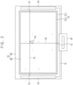
- FIG. 2 is a plan view illustrating a display device according to an embodiment.
- the display device may include a display panel 10 and a driving film DF.
- the display portion DP may include data lines DL and scan lines SL.
- the pixels PX may be connected to the data lines DL and the scan lines SL.
- the data lines DL may transmit the data signal DS
- the scan lines SL may transmit the scan signal SS.
- the data lines DL and the scan lines SL may extend in directions intersecting each other.
- the peripheral portion PP may include power voltage lines PL.
- the power voltage lines PL may include a first power voltage line PL1 and a second power voltage line PL2.
- the first power voltage line PL1 may transmit the first power voltage VDD
- the second power voltage line PL2 may transmit the second power voltage VSS.
- the driving film DF may be connected to the peripheral portion PP of the display panel 10.
- the driving film DF may include a driving chip such as an integrated circuit (IC) chip or the like.
- the scan driver 22 may be disposed in the peripheral portion PP of the display panel 10, and the driving film DF may include the data driver 21 and the controller 30.
- connection line CL connecting the display portion DP and the driver 20 or connecting the driver 20 and the controller 30 may be disposed in the peripheral portion PP of the display panel 10.
- the connection line CL may connect the scan line SL to the scan driver 22, the data line DL to the data driver 21, or the scan driver 22 to the controller 30.
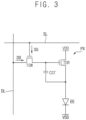
- FIG. 3 is a circuit diagram illustrating a pixel PX included in a display device according to an embodiment.
- the pixel PX may be connected to the data line DL and the scan line SL.
- the pixel PX may include a driving transistor TDR, a switching transistor TSW, a storage capacitor CST, and a light emitting element EE.
- a first electrode of the switching transistor TSW may receive the data signal DS, and a second electrode of the switching transistor TSW may be connected to the driving transistor TDR.
- a gate electrode of the switching transistor TSW may receive the scan signal SS.
- the switching transistor TSW may provide the data signal DS to the driving transistor TDR in response to the scan signal SS.
- a first electrode of the driving transistor TDR may receive the first power voltage VDD, and a second electrode of the driving transistor TDR may be connected to the light emitting element EE.
- a gate electrode of the driving transistor TDR may be connected to the second electrode of the switching transistor TSW.
- the driving transistor TDR may generate a driving current corresponding to a voltage stored in the storage capacitor CST using the first power voltage VDD, and may provide the driving current to the light emitting element EE.
- each of the switching transistor TSW and the driving transistor TDR is illustrated as an NMOS transistor, at least one of the switching transistor TSW and the driving transistor TDR may be a PMOS transistor.
- the first electrode of each of the switching transistor TSW and the driving transistor TDR may be one of a source electrode and a drain electrode, and the second electrode of each of the switching transistor TSW and the driving transistor TDR may be the other of the source electrode and the drain electrode.
- the storage capacitor CST may be connected between the gate electrode of the driving transistor TDR and the second electrode of the driving transistor TDR.
- the storage capacitor CST may store a voltage corresponding to the data signal DS.
- the first electrode of the light emitting element EE may be connected to the second electrode of the driving transistor TDR, and the second electrode of the light emitting element EE may receive the second power voltage VSS.
- the light emitting element EE may emit light based on the driving current.
- the pixel PX including two transistors and one capacitor is illustrated, however, components of the pixel PX are not limited thereto.
- the pixel PX may include three or more transistors and may include two or more capacitors.
- FIG. 4 is a cross-sectional view illustrating the pixel PX in FIG. 3 .
- the pixel PX may include a substrate 100, transistors disposed on the substrate 100 and including the driving transistor TDR, and the light emitting element EE connected to the driving transistor TDR.
- the driving transistor TDR may include an active layer 111, a gate electrode 121, a first electrode 133, and a second electrode 134.
- the light emitting element EE may include a pixel electrode 140, an emission layer 150, and an opposite electrode 160.
- the substrate 100 may include glass, plastic, metal, or the like.
- a light blocking layer BML may be disposed on the substrate 100.
- the light blocking layer BML may block external light from being introduced into the active layer 111.
- the light blocking layer BML may include a metal.
- the metal may include molybdenum (Mo), aluminum (Al), copper (Cu), titanium (Ti), or the like.
- a buffer layer 101 may be disposed on the light blocking layer BML.
- the buffer layer 101 may cover the light blocking layer BML on the substrate 100.
- the buffer layer 101 may block impurities from flowing into the active layer 111, and may planarize a portion over the substrate 100.
- the buffer layer 101 may include an inorganic insulating material.
- the inorganic insulating material may include silicon oxide, silicon nitride, silicon oxynitride, or the like.
- the active layer 111 may be disposed on the buffer layer 101.
- the active layer 111 may include an oxide semiconductor.
- the oxide semiconductor may include an oxide of at least one selected from the group of indium (In), gallium (Ga), tin (Sn), zirconium (Zr), vanadium (V), hafnium (Hf), cadmium (Cd), germanium (Ge), chromium (Cr), titanium (Ti), and zinc (Zn).
- the oxide semiconductor may include at least one of zinc oxide (ZnO), zinc-tin oxide (ZTO), zinc-indium oxide (ZIO), indium oxide (InO), titanium oxide (TiO), indium-gallium-zinc oxide (IGZO), and indium-zinc-tin oxide (IZTO).
- the active layer 111 may include amorphous silicon, polycrystalline silicon, or the like.
- the active layer 111 may include a first region 111a, a second region 111b, and a channel region 111c.
- the second region 111b may be spaced apart from the first region 111a.
- the channel region 111c may be disposed between the first region 111a and the second region 111b.
- Each of the first region 111a and the second region 111b may be doped with impurities, and the channel region 111c may not be doped with the impurities.
- the impurities may be N-type impurities.
- the N-type impurities may include phosphorus (P), arsenic (As), antimony (Sb), or the like.
- the impurities may be P-type impurities.
- a gate insulating layer 102 may be disposed on the active layer 111.
- the gate insulating layer 102 may include an inorganic insulating material.
- the inorganic insulating material may include silicon oxide, silicon nitride, silicon oxynitride, or the like.
- the gate electrode 121 may be disposed on the gate insulating layer 102.
- the gate electrode 121 may overlap the channel region 111c of the active layer 111.
- the gate electrode 121 may include a metal.
- the metal may include molybdenum (Mo), aluminum (Al), copper (Cu), titanium (Ti), or the like.
- the gate electrode 121 may have a single-layer structure or a multilayer structure.
- An interlayer insulating layer 103 may be disposed on the gate electrode 121.
- the interlayer insulating layer 103 may cover the active layer 111 and the gate electrode 121 on the buffer layer 101.
- the interlayer insulating layer 103 may include an inorganic insulating material.
- the inorganic insulating material may include silicon oxide, silicon nitride, silicon oxynitride, or the like.
- the first electrode 133 may be disposed on the interlayer insulating layer 103.
- the first electrode 133 may be electrically connected to the first region 111a of the active layer 111.
- the first electrode 133 may contact the first region 111a of the active layer 111 through a contact hole penetrating the interlayer insulating layer 103.
- the second electrode 134 may be disposed on the interlayer insulating layer 103.
- the second electrode 134 may be electrically connected to the second region 111b of the active layer 111.
- the second electrode 134 may contact the second region 111b of the active layer 111 through a contact hole penetrating the interlayer insulating layer 103.
- each of the first electrode 133 and the second electrode 134 may include a metal.
- the metal may include molybdenum (Mo), aluminum (Al), copper (Cu), titanium (Ti), or the like.
- Mo molybdenum
- Al aluminum
- Cu copper
- Ti titanium
- Each of the first electrode 133 and the second electrode 134 may have a single-layer structure or a multilayer structure.
- a planarization layer 104 may be disposed on the first electrode 133 and the second electrode 134.
- the planarization layer 104 may cover the first electrode 133 and the second electrode 134 on the interlayer insulating layer 103.
- the planarization layer 104 may have a flat upper surface.
- the planarization layer 104 may include an organic insulating material and/or an inorganic insulating material.
- the pixel electrode 140 may be disposed on the planarization layer 104.
- the pixel electrode 140 may be electrically connected to the second electrode 134.
- the pixel electrode 140 may contact the second electrode 134 through a contact hole penetrating the planarization layer 104.
- the pixel electrode 140 may include a transparent conductive oxide.
- the transparent conductive oxide may include at least one selected from the group including indium-tin oxide (ITO), indium-zinc oxide (IZO), indium oxide (InO), indium-gallium oxide (IGO), and aluminum-zinc oxide (AZO).
- the pixel electrode 140 may further include a metal as well as the transparent conductive oxide.
- the metal may include at least one selected from the group including silver (Ag), magnesium (Mg), aluminum (Al), platinum (Pt), lead (Pd), gold (Au), nickel (Ni), niobium (Nd), iridium (Ir), and chromium (Cr).
- a pixel defining layer 105 may be disposed on the pixel electrode 140.
- the pixel defining layer 105 may cover the pixel electrode 140 on the planarization layer 104.
- the pixel defining layer 105 may have an opening OP exposing at least a portion of the pixel electrode 140.
- the opening OP may define an area in which the pixel PX is disposed in a plan view.
- the opening OP may expose a central portion of the pixel electrode 140, and the pixel defining layer 105 may cover an edge of the pixel electrode 140.
- the pixel defining layer 105 may include an organic insulating material and/or an inorganic insulating material.
- the emission layer 150 may be disposed on the pixel electrode 140.
- the emission layer 150 may be disposed on the pixel electrode 140 exposed by the opening OP of the pixel defining layer 105.
- the emission layer 150 may include at least one of an organic light emitting material and a quantum dot.
- the organic light emitting material may include a low molecular weight organic compound or a high molecular weight organic compound.
- the low molecular weight organic compound may include copper phthalocyanine, N,N'-diphenylbenzidine, tris-(8-hydroxyquinoline)aluminum, etc.
- the high molecular weight organic compound may include poly(3,4-ethylenedioxythiophene), polyaniline, poly-phenylenevinylene, polyfluorene, etc.
- the quantum dot may include a core including a group II-VI compound, a group III-V compound, a group IV-VI compound, a group IV element, a group IV compound, and combinations thereof.
- the quantum dot may have a core-shell structure including the core and a shell surrounding the core. The shell may serve as a protective layer for maintaining semiconductor properties by preventing chemical modification of the core and as a charging layer for imparting electrophoretic properties to the quantum dot.
- the opposite electrode 160 may be disposed on the emission layer 150 and the pixel defining layer 105.
- the opposite electrode 160 may include a metal.
- the metal may include at least one selected from the group including silver (Ag), magnesium (Mg), aluminum (Al), platinum (Pt), lead (Pd), gold (Au), nickel (Ni), niobium (Nd), iridium (Ir), chromium (Cr), lithium (Li), and calcium (Ca).
- FIG. 5 is a diagram illustrating discharge diodes ED included in a display device according to an embodiment.
- a discharge diode ED may be connected to the connection line CL.
- the static electricity may damage elements in the display portion DP.
- the gate insulating layer 102 of the transistor included in the pixel PX may be damaged by the static electricity.
- the discharge diode ED may discharge static electricity flowing into the connection line CL.
- one of a first electrode and a second electrode of the discharge diode ED may be connected to the connection line CL, and the other of the first electrode and the second electrode of the discharge diode ED may be connected to the power voltage line PL.
- the discharge diodes ED may include a first discharge diode ED1 and a second discharge diode ED2.
- a first electrode of the first discharge diode ED1 may be connected to the second power voltage line PL2, and a second electrode of the first discharge diode ED1 may be connected to the connection line CL.
- a first electrode of the second discharge diode ED2 may be connected to the connection line CL, and a second electrode of the second discharge diode ED2 may be connected to the first power voltage line PL1.
- a voltage level of each of the driving signal and the control signal transmitted through the connection line CL may be higher than a voltage level of the second power voltage VSS, and may be lower than a voltage level of the first power voltage VDD. Accordingly, when the driving signal or the control signal is transmitted through the connection line CL, the first discharge diode ED1 and the second discharge diode ED2 may be turned off.
- the second discharge diode ED2 when static electricity having a voltage level higher than the voltage level of the first power voltage VDD is introduced into the connection line CL, the second discharge diode ED2 may be turned on, and the static electricity may be discharged to the first power voltage line PL1 through the second discharge diode ED2. Further, when static electricity having a voltage level lower than the voltage level of the second power voltage VSS is introduced into the connection line CL, the first discharge diode ED1 may be turned on, and the static electricity may be discharged to the second power voltage line PL2 through the first discharge diode ED1.
- FIG. 6 is a circuit diagram illustrating transistors TR included in a display device according to an embodiment.
- the discharge diode ED includes a transistor TR in which a second electrode and a gate electrode are connected.
- the transistor TR may operate as a diode.
- the transistor TR in which the second electrode and the gate electrode are connected may be referred to as a diode-connected transistor.
- one of a first electrode and a second electrode of the transistor TR may be connected to the connection line CL, and the other of the first electrode and the second electrode of the transistor TR may be connected to the power voltage line PL.
- the first discharge diode ED1 may include a first transistor TR1
- the second discharge diode ED2 may include a second transistor TR2.
- a first electrode of the first transistor TR1 may be connected to the second power voltage line PL2
- a second electrode of the first transistor TR1 may be connected to the connection line CL
- a gate electrode of the first transistor TR1 may be connected to the second electrode of the first transistor TR1.
- the first electrode of the second transistor TR2 may be connected to the connection line CL
- the second electrode of the second transistor TR2 may be connected to the first power voltage line PL1
- a gate electrode of the second transistor TR2 may be connected to the second electrode of the second transistor TR2.
- the transistor TR is illustrated as an NMOS transistor, however, the transistor TR may be a PMOS transistor.
- the first electrode of the transistor TR may be one of a source electrode and a drain electrode, and the second electrode of the transistor TR may be the other of the source electrode and the drain electrode.
- FIG. 7 is a plan view illustrating a transistor according to an embodiment.
- FIG. 8 is a cross-sectional view illustrating the transistor taken along a line I-I' in FIG. 7 .
- the transistor TR includes an active layer 110, a gate electrode 120, a first electrode 131, a second electrode 132, a first connection electrode CE1, and it may include a second connection electrode CE2.
- the active layer 110 may be disposed on the buffer layer 101.
- the active layer 110 may include an oxide semiconductor.
- the oxide semiconductor may include an oxide of at least one selected from the group including indium (In), gallium (Ga), tin (Sn), zirconium (Zr), vanadium (V), hafnium (Hf), cadmium (Cd), germanium (Ge), chromium (Cr), titanium (Ti), and zinc (Zn).
- the oxide semiconductor may include at least one of zinc oxide (ZnO), zinc-tin oxide (ZTO), zinc-indium oxide (ZIO), indium oxide (InO), titanium oxide (TiO), indium-gallium-zinc oxide (IGZO), and indium-zinc-tin oxide (IZTO).
- the active layer 110 may include amorphous silicon, polycrystalline silicon, or the like.
- the active layer 110 includes a first region 110a, a second region 110b, and a channel region 110c.
- the second region 110b may be spaced apart from the first region 110a.
- the channel region 110c is disposed between the first region 110a and the second region 110b.
- Each of the first region 110a and the second region 110b may be doped with impurities, and the channel region 110c may not be doped with the impurities.
- the impurities may be N-type impurities.
- the N-type impurities may include phosphorus (P), arsenic (As), antimony (Sb), or the like.
- the impurities may be P-type impurities.
- the gate electrode 120 may be disposed on the gate insulating layer 102.
- the gate electrode 120 may overlap the channel region 110c of the active layer 110.
- the gate electrode 120 may include a metal.
- the metal may include molybdenum (Mo), aluminum (Al), copper (Cu), titanium (Ti), or the like.
- the gate electrode 120 may have a single-layer structure or a multilayer structure.
- the first electrode 131 is disposed on the interlayer insulating layer 103.
- the first electrode 131 is electrically connected to the first region 110a of the active layer 110.
- the first electrode 131 may contact the first region 110a of the active layer 110 through a first contact hole CH1 penetrating the interlayer insulating layer 103.
- the second electrode 132 is disposed on the interlayer insulating layer 103.
- the second electrode 132 is electrically connected to the second region 110b of the active layer 110.
- the second electrode 132 may contact the second region 110b of the active layer 110 through a second contact hole CH2 penetrating the interlayer insulating layer 103.
- each of the first electrode 131 and the second electrode 132 may include a metal.
- the metal may include molybdenum (Mo), aluminum (Al), copper (Cu), titanium (Ti), or the like.
- Mo molybdenum
- Al aluminum
- Cu copper
- Ti titanium
- Each of the first electrode 131 and the second electrode 132 may have a single-layer structure or a multilayer structure.
- the first connection electrode CE1 may be disposed at the same layer as the active layer 110. In other words, the first connection electrode CE1 may be disposed on the buffer layer 101.
- the first connection electrode CE1 electrically connects the gate electrode 120 and the second electrode 132. In an embodiment, the second electrode 132 may contact the first connection electrode CE1 through a third contact hole CH3 penetrating the interlayer insulating layer 103.
- the first connection electrode CE1 may include an oxide semiconductor.
- the oxide semiconductor may include an oxide of at least one selected from the group including indium (In), gallium (Ga), tin (Sn), zirconium (Zr), vanadium (V), hafnium (Hf), cadmium (Cd), germanium (Ge), chromium (Cr), titanium (Ti), and zinc (Zn).
- the oxide semiconductor may include zinc oxide (ZnO), zinc-tin oxide (ZTO), zinc-indium oxide (ZIO), indium oxide (InO), titanium oxide (TiO), indium-gallium-zinc oxide (IGZO), and indium-zinc-tin oxide (IZTO).
- the first connection electrode CE1 may include amorphous silicon, polycrystalline silicon, or the like.
- the first connection electrode CE1 may be doped with impurities.
- the impurities may be N-type impurities.
- the N-type impurities may include phosphorus (P), arsenic (As), antimony (Sb), or the like.
- the impurities may be P-type impurities.
- a resistance of the first connection electrode CE1 is greater than a resistance of the gate electrode 120.
- the first connection electrode CE1 may include an oxide semiconductor, and the gate electrode 120 may include a metal. In such an embodiment, since a resistivity of the oxide semiconductor is greater than a resistivity of the metal, the resistance of the first connection electrode CE1 may be greater than the resistance of the gate electrode 120.
- the second connection electrode CE2 may be disposed at the same layer as the first electrode 131 and the second electrode 132. In other words, the second connection electrode CE2 may be disposed on the interlayer insulating layer 103.
- the second connection electrode CE2 may contact the first connection electrode CE1 through a fourth contact hole CH4 penetrating the interlayer insulating layer 103, and may contact the gate electrode 120 through a fifth contact hole CH5 penetrating the interlayer insulating layer 103.
- the second connection electrode CE2 may include a metal.
- the metal may include molybdenum (Mo), aluminum (Al), copper (Cu), titanium (Ti), or the like.
- Mo molybdenum
- Al aluminum
- Cu copper
- Ti titanium
- the second connection electrode CE2 may have a single-layer structure or a multilayer structure.
- the gate electrode of the transistor which has a relatively small resistance
- static electricity supplied to the second electrode may flow into the active layer through the second electrode, the gate electrode, and the gate insulating layer.
- the gate electrode and the active layer may be electrically shorted by the static electricity, and accordingly, the transistor may be damaged by the static electricity.
- the gate electrode 120 and the second electrode 132 of the transistor TR are electrically connected by the first connection electrode CE1, which has a relatively large resistance. If static electricity is supplied to the second electrode 132, the static electricity may not flow into the active layer 110 through the second electrode 132, the gate electrode 120, and the gate insulating layer 102 because of the relatively large resistance of the first connection electrode CE1. Accordingly, the transistor TR may not be damaged by the static electricity.
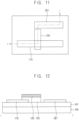
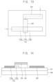
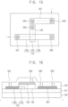
- FIGS. 9, 10 , 11, 12 , 13, 14 , 15, and 16 are diagrams illustrating a method of manufacturing a transistor according to an embodiment.
- FIGS. 9 to 16 may illustrate a method of manufacturing the transistor TR in FIGS. 7 and 8 .
- the active layer 110 and the first connection electrode CE1 may be formed on the buffer layer 101.
- the first connection electrode CE1 may be spaced apart from the active layer 110.
- an oxide semiconductor layer may be formed on the buffer layer 101, and the oxide semiconductor layer may be patterned to substantially simultaneously form the active layer 110 and the first connection electrode CE1.
- the gate insulating layer 102 and the gate electrode 120 may be formed on the active layer 110 and the first connection electrode CE1.
- an insulating layer and a metal layer may be sequentially formed on the active layer 110 and the first connection electrode CE1, and the insulating layer and the metal layer may be patterned together to substantially simultaneously form the gate insulating layer 102 and the gate electrode 120.
- the active layer 110 and the first connection electrode CE1 may be doped with impurities.
- N-type impurities may be doped into the active layer 110 and the first connection electrode CE1 using the gate electrode 120 as a mask.
- the impurities may be doped into the first region 110a and the second region 110b of the active layer 110 which do not overlap the gate electrode 120, and the impurities may not be doped into the channel region 110c of the active layer 110 which overlaps the gate electrode 120.
- the interlayer insulating layer 103 is formed on the gate electrode 120, and the first to fifth contact holes CH1 to CH5 penetrating the interlayer insulating layer 103 may be formed.
- the first contact hole CH1 may expose the first region 110a of the active layer 110
- the second contact hole CH2 may expose the second region 110b of the active layer 110.
- the third contact hole CH3 may expose a first end of the first connection electrode CE1
- the fourth contact hole CH4 may expose a second end of the first connection electrode CE1.
- the fifth contact hole CH5 may expose the gate electrode 120.
- the first electrode 131, the second electrode 132, and the second connection electrode CE2 are formed on the interlayer insulating layer 103.
- the first electrode 131 may contact the first region 110a of the active layer 110 through the first contact hole CH1.
- the second electrode 132 may contact the second region 110b of the active layer 110 through the second contact hole CH2, and may contact the first end of the first connection electrode CE1 through the third contact hole CH3.
- the second connection electrode CE2 may contact the second end of the first connection electrode CE1 through the fourth contact hole CH4, and may contact the gate electrode 120 through the fifth contact hole CH5.
- a metal layer may be formed on the interlayer insulating layer 103, and the metal layer may be patterned to substantially simultaneously form the first electrode 131, the second electrode 132, and the second connection electrode CE2.
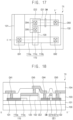
- FIG. 17 is a plan view illustrating a transistor according to an embodiment.
- FIG. 18 is a cross-sectional view illustrating the transistor taken along a line II-II' in FIG. 17 .
- a transistor TR includes an active layer 110, a gate electrode 120, a first electrode 131, a second electrode 132, a first connection electrode CE1, and it may include a second connection electrode CE2, and a dummy pattern DM.
- the transistor TR described with reference to FIGS. 17 and 18 may be substantially the same as or similar to the transistor TR described with reference to FIGS. 7 and 8 , except for further including the dummy pattern DM. Accordingly, descriptions of the overlapping components will be omitted.
- a resistance of the non-impurity region CE1b may be greater than a resistance of the impurity region CE1a. As the impurities are doped into the impurity region CE1a, the resistance of the impurity region CE1a may decrease. Accordingly, the resistance of the impurity region CE1a may be less than the resistance of the non-impurity region CE1b into which the impurities are not doped.
- the dummy pattern DM may be disposed at the same layer as the gate electrode 120. In other words, the dummy pattern DM may be disposed on the gate insulating layer 102.
- the dummy pattern DM may overlap a portion of the first connection electrode CE1. Specifically, the dummy pattern DM may overlap the non-impurity region CE1b of the first connection electrode CE1.
- the dummy pattern DM may include a metal.
- the metal may include molybdenum (Mo), aluminum (Al), copper (Cu), titanium (Ti), or the like.
- Mo molybdenum
- Al aluminum
- Cu copper
- Ti titanium
- the dummy pattern DM may have a single-layer structure or a multilayer structure.
- the resistance of the first connection electrode CE1 may increase. Accordingly, as the gate electrode 120 and the second electrode 132 of the transistor TR are electrically connected by the first connection electrode CE1 having a relatively large resistance, although static electricity is supplied to the second electrode 132, the static electricity may not flow into the active layer 110 through the second electrode 132, the gate electrode 120, and the gate insulating layer 102.
- FIGS. 19, 20 , 21, and 22 are diagrams illustrating a method of manufacturing a transistor according to an embodiment.
- FIGS. 19 to 22 may illustrate a method of manufacturing the transistor TR in FIGS. 17 and 18 .
- Descriptions of components of the method of manufacturing the transistor TR described with reference to FIGS. 19 to 22 which are substantially the same as or similar to those of the method of manufacturing the transistor TR described with reference to FIGS. 7 to 16 , will be omitted.
- the gate insulating layer 102, the gate electrode 120, and the dummy pattern DM may be formed on the active layer 110 and the first connection electrode CE1.
- an insulating layer and a metal layer may be sequentially formed on the active layer 110 and the first connection electrode CE1, and the insulating layer and the metal layer may be patterned together to substantially simultaneously form the gate insulating layer 102, the gate electrode 120, and the dummy pattern DM.
- the active layer 110 and the first connection electrode CE1 may be doped with impurities.
- N-type impurities may be doped into the active layer 110 and the first connection electrode CE1 by using the gate electrode 120 and the dummy pattern DM as a mask.
- the impurity region CE1a of the first connection electrode CE1, which does not overlap the dummy pattern DM, may be doped with the impurities, and the non-impurity region CE1b of the first connection electrode CE1, which overlaps the dummy pattern DM, may not be doped with the impurities.
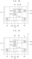
- FIG. 23 is a plan view illustrating a transistor according to an embodiment.
- a transistor TR includes an active layer 110, a gate electrode 120, a first electrode 131, a second electrode 132, a first connection electrode CE1, and it may include a second connection electrode CE2, and a plurality of dummy patterns DM.
- the transistor TR described with reference to FIG. 23 may be substantially the same as or similar to the transistor TR described with reference to FIGS. 17 and 18 except for including the plurality of dummy patterns DM. Accordingly, descriptions of the overlapping components will be omitted.
- the dummy patterns DM may be disposed at the same layer as the gate electrode 120. Each of the dummy patterns DM may overlap a portion of the first connection electrode CE1. Impurities may not be doped into portions of the first connection electrode CE1 respectively overlapping the dummy patterns DM, and accordingly, the first connection electrode CE1 may include a plurality of non-impurity regions.
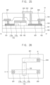
- FIG. 24 is a plan view illustrating a transistor according to an embodiment.
- FIG. 25 is a cross-sectional view illustrating the transistor taken along a line III-III' in FIG. 24 .
- a transistor TR includes an active layer 110, a gate electrode 120, a first electrode 131, a second electrode 132, a first connection electrode CE1, and it may include a second connection electrode CE2.
- the transistor TR described with reference to FIGS. 24 and 25 may be substantially the same as or similar to the transistor TR described with reference to FIGS. 7 and 8 except for the position of the second connection electrode CE2. Accordingly, descriptions of the overlapping components will be omitted.
- the second connection electrode CE2 may be disposed on the first electrode 131 and the second electrode 132. In an embodiment, the second connection electrode CE2 may be disposed at the same layer as the pixel electrode 140 in FIG. 4 . In other words, the second connection electrode CE2 may be disposed on the planarization layer 104. The second connection electrode CE2 may contact the first connection electrode CE1 through a fourth contact hole CH4 penetrating the planarization layer 104 and the interlayer insulating layer 103, and may contact the gate electrode 120 through a fifth contact hole CH5 penetrating the planarization layer 104 and the interlayer insulating layer 103.
- the second connection electrode CE2 may include a transparent conductive oxide.
- the transparent conductive oxide may include at least one selected from the group including indium-tin oxide (ITO), indium-zinc oxide (IZO), indium oxide (InO), indium-gallium oxide (IGO), and aluminum-zinc oxide (AZO).
- the second connection electrode CE2 may further include a metal as well as the transparent conductive oxide.
- the metal may include at least one selected from the group including silver (Ag), magnesium (Mg), aluminum (Al), platinum (Pt), lead (Pd), gold (Au), nickel (Ni), niobium (Nd), iridium (Ir), and chromium (Cr).
- a resistance of the second connection electrode CE2 may be greater than a resistance of the gate electrode 120.
- the second connection electrode CE2 may include a transparent conductive oxide
- the gate electrode 120 may include a metal.
- the resistance of the second connection electrode CE2 may be greater than the resistance of the gate electrode 120.
- the gate electrode 120 and the second electrode 132 of the transistor TR are electrically connected by the first connection electrode CE1 having a relatively large resistance and may be electrically connected by the the second connection electrode CE2 having a relatively large resistance. Therefore, although static electricity is supplied to the second electrode 132, static electricity may not be introduced to the active layer 110 through the second electrode 132, the gate electrode 120, and the gate insulating layer 102. Accordingly, the transistor TR may not be damaged by the static electricity.
- FIGS. 26 , 27 , 28 , 29 , 30 , and 31 are diagrams illustrating a method of manufacturing a transistor according to an embodiment.
- FIGS. 26 to 31 may illustrate a method of manufacturing the transistor TR in FIGS. 24 and 25 .
- Descriptions of components of the method of manufacturing the transistor TR described with reference to FIGS. 24 to 31 which are substantially the same as or similar to those of the method of manufacturing the transistor TR described with reference to FIGS. 7 to 16 , will be omitted.
- the interlayer insulating layer 103 is formed on the gate electrode 120, and the first to third contact holes CH1 to CH3 penetrating the interlayer insulating layer 103 may be formed.
- the first contact hole CH1 may expose the first region 110a of the active layer 110
- the second contact hole CH2 may expose the second region 110b of the active layer 110.
- the third contact hole CH3 may expose a first end of the first connection electrode CE1.
- the first electrode 131 and the second electrode 132 are formed on the interlayer insulating layer 103.
- the first electrode 131 may contact the first region 110a of the active layer 110 through the first contact hole CH1.
- the second electrode 132 may contact the second region 110b of the active layer 110 through the second contact hole CH2, and may contact the first end of the first connection electrode CE1 through the third contact hole CH3.
- a metal layer may be formed on the interlayer insulating layer 103, and the metal layer may be patterned to substantially simultaneously form the first electrode 131 and the second electrode 132.
- the planarization layer 104 may be formed on the first electrode 131 and the second electrode 132, and fourth and fifth contact holes CH4 and CH5 penetrating the planarization layer 104 and the interlayer insulating layer 103 may be formed.
- the fourth contact hole CH4 may expose a second end of the first connection electrode CE1
- the fifth contact hole CH5 may expose the gate electrode 120.
- the second connection electrode CE2 may be formed on the planarization layer 104.
- the second connection electrode CE2 may contact the second end of the first connection electrode CE1 through the fourth contact hole CH4, and may contact the gate electrode 120 through the fifth contact hole CH5.
- a transparent conductive oxide layer may be formed on the planarization layer 104, and the transparent conductive oxide layer may be patterned to form the second connection electrode CE2.
- FIG. 32 is a plan view illustrating a transistor according to an embodiment.
- FIG. 33 is a cross-sectional view illustrating the transistor taken along a line IV-IV' in FIG. 32 .
- a transistor TR includes an active layer 110, a gate electrode 120, a first electrode 131, a second electrode 132, and a first connection electrode CE1.
- the transistor TR described with reference to FIGS. 32 and 33 may be substantially the same as or similar to the transistor TR described with reference to FIGS. 7 and 8 except for the position of the first connection electrode CE1 and the omission of the second connection electrode CE2. Accordingly, descriptions of the overlapping components will be omitted.
- the first connection electrode CE1 may be disposed on the first electrode 131 and the second electrode 132. In an embodiment, the first connection electrode CE1 may be disposed at the same layer as the pixel electrode 140 in FIG. 4 . In other words, the first connection electrode CE1 may be disposed on the planarization layer 104. The first connection electrode CE1 may contact the second electrode 132 through a third contact hole CH3 penetrating the planarization layer 104, and may contact the gate electrode 120 through a fourth contact hole CH4 penetrating the planarization layer 104 and the interlayer insulating layer 103.
- the first connection electrode CE1 may include a transparent conductive oxide.
- the transparent conductive oxide may include at least one selected from the group including indium-tin oxide (ITO), indium-zinc oxide (IZO), indium oxide (InO), indium-gallium oxide (IGO), and aluminum-zinc oxide (AZO).
- the first connection electrode CE1 may further include a metal as well as the transparent conductive oxide.
- the metal may include at least one selected from the group including silver (Ag), magnesium (Mg), aluminum (Al), platinum (Pt), lead (Pd), gold (Au), nickel (Ni), niobium (Nd), iridium (Ir), and chromium (Cr).
- a resistance of the first connection electrode CE1 is greater than a resistance of the gate electrode 120.
- the first connection electrode CE1 may include a transparent conductive oxide
- the gate electrode 120 may include a metal.
- the resistance of the first connection electrode CE1 may be greater than the resistance of the gate electrode 120.
- FIG. 34 is a plan view illustrating a transistor according to an embodiment.
- FIG. 35 is a cross-sectional view illustrating the transistor taken along a line V-V' in FIG. 34 .
- a transistor TR includes an active layer 110, a gate electrode 120, a first electrode 131, a second electrode 132, a first connection electrode CE1, it may include a second connection electrode CE2.
- the transistor TR described with reference to FIGS. 34 and 35 may be substantially the same as or similar to the transistor TR described with reference to FIGS. 32 and 33 except for the addition of the second connection electrode CE2. Accordingly, descriptions of the overlapping components will be omitted.
- the second connection electrode CE2 may be disposed at the same layer as the first electrode 131 and the second electrode 132. In other words, the second connection electrode CE2 may be disposed on the interlayer insulating layer 103.
- the second connection electrode CE2 may contact the first connection electrode CE1 through a fourth contact hole CH4 penetrating the planarization layer 104, and may contact the gate electrode 120 through a fifth contact hole CH5 penetrating the interlayer insulating layer 103.
- the second connection electrode CE2 may include a metal.
- the metal may include molybdenum (Mo), aluminum (Al), copper (Cu), titanium (Ti), or the like.
- Mo molybdenum
- Al aluminum
- Cu copper
- Ti titanium
- the second connection electrode CE2 may have a single-layer structure or a multilayer structure.
- a transistor including: a substrate; an active layer disposed on the substrate and including a first region, a second region, and a channel region between the first region and the second region; a gate electrode disposed on the active layer, the gate electrode overlapping the channel region; a first electrode disposed on the substrate, the first electrode being electrically connected to the first region; a second electrode disposed on the substrate, the second electrode being electrically connected to the second region; and a first connection electrode disposed on the substrate and electrically connecting the gate electrode and the second electrode.
- embodiments provide a display device, comprising: a display portion including a substrate and a plurality of pixels disposed on the substrate; a driver configured to provide a driving signal to the display portion; a controller configured to provide a control signal to the driver; and a transistor connected to a connection line connecting the display portion and the driver or connecting the driver and the controller, the transistor being as set out in any of the above embodiments.
- the gate electrode and the second electrode of the transistor are electrically connected by a first connection electrode having a relatively large resistance.
- the static electricity may not flow into the active layer through the second electrode, the gate electrode, and the gate insulating layer. Accordingly, the transistor may not be damaged by the static electricity.
- the transistor and the display device according to the embodiments may be applied to a display device included in a computer, a notebook, a mobile phone, a smart phone, a smart pad, a PMP, a PDA, an MP3 player, or the like.
Landscapes
- Engineering & Computer Science (AREA)
- Microelectronics & Electronic Packaging (AREA)
- Physics & Mathematics (AREA)
- Geometry (AREA)
- Devices For Indicating Variable Information By Combining Individual Elements (AREA)
Claims (14)
- Transistor (TR), umfassend:ein Substrat (100);eine aktive Schicht (110), die auf dem Substrat angeordnet ist und eine erste Region (110a), eine zweite Region (110b) und eine Kanalregion (110c) zwischen der ersten Region und der zweiten Region enthält;eine Gate-Elektrode (120), die auf der aktiven Schicht angeordnet ist, wobei die Gate-Elektrode die Kanalregion überlappt;eine Isolierschicht (103), die auf der Gate-Elektrode angeordnet ist;eine erste Elektrode (131), die auf der Isolierschicht angeordnet ist, wobei die erste Elektrode elektrisch mit der ersten Region verbunden ist;eine zweite Elektrode (132), die auf der Isolierschicht angeordnet ist, wobei die zweite Elektrode elektrisch mit der zweiten Region verbunden ist; undeine erste Verbindungselektrode (CE1), die auf dem Substrat angeordnet ist und die Gate-Elektrode und die zweite Elektrode elektrisch verbindet, dadurch gekennzeichnet, dassein Widerstand der ersten Verbindungselektrode größer als ein Widerstand der Gate-Elektrode ist.
- Transistor nach Anspruch 1, wobei die erste Verbindungselektrode auf einer gleichen Schicht wie die aktive Schicht angeordnet ist.
- Transistor nach Anspruch 2, wobei die erste Verbindungselektrode einen Oxidhalbleiter enthält.
- Transistor nach Anspruch 2 oder 3, ferner umfassend:
eine zweite Verbindungselektrode (CE2), die auf der Gate-Elektrode angeordnet ist, wobei die zweite Verbindungselektrode die erste Verbindungselektrode und die Gate-Elektrode kontaktiert. - Transistor nach Anspruch 4, wobei die erste Verbindungselektrode die zweite Verbindungselektrode und die zweite Elektrode kontaktiert; oder wobei die zweite Verbindungselektrode auf einer gleichen Schicht wie die zweite Elektrode angeordnet ist.
- Transistor nach Anspruch 4 oder 5, wobei die zweite Verbindungselektrode auf der zweiten Elektrode angeordnet ist.
- Transistor nach einem der Ansprüche 2 bis 6, ferner umfassend:ein Dummy-Muster (DM), das auf einer gleichen Schicht wie die Gate-Elektrode angeordnet ist, wobei das Dummy-Muster einen Abschnitt der ersten Verbindungselektrode überlappt;optional wobei eine Störstelle in dem Abschnitt der ersten Verbindungselektrode nicht dotiert ist.
- Transistor nach einem der Ansprüche 1 bis 7, wobei die erste Verbindungselektrode auf der zweiten Elektrode angeordnet ist;optional wobei die erste Verbindungselektrode ein transparentes leitendes Oxid enthält;optional wobei die erste Verbindungselektrode die Gate-Elektrode und die zweite Elektrode kontaktiert.
- Transistor nach Anspruch 8, ferner umfassend:eine zweite Verbindungselektrode (CE2), die auf einer gleichen Schicht wie die zweite Elektrode angeordnet ist, wobei die zweite Verbindungselektrode die Gate-Elektrode und die erste Verbindungselektrode kontaktiert;optional wobei die erste Verbindungselektrode die zweite Verbindungselektrode und die zweite Elektrode kontaktiert.
- Anzeigevorrichtung, umfassend:einen Anzeigeabschnitt (DP), der ein Substrat und eine Vielzahl von Pixeln (PX), die auf dem Substrat angeordnet sind, enthält;einen Treiber (20), der dazu konfiguriert ist, dem Anzeigeabschnitt ein Antriebssignal bereitzustellen;eine Steuerung (30), die dazu konfiguriert ist, ein Steuersignal dem Treiber bereitzustellen; undeinen Transistor (TR), der mit einer Verbindungsleitung (CL) verbunden ist, die den Anzeigeabschnitt und den Treiber verbindet oder den Treiber und die Steuerung verbindet, wobei der Transistor wie in den Ansprüchen 1 bis 9 dargelegt ist.
- Anzeigevorrichtung nach Anspruch 10, wobei eine von der ersten Elektrode und der zweiten Elektrode mit der Verbindungsleitung verbunden ist, und
wobei die andere von der ersten Elektrode und der zweiten Elektrode mit einer Leistungsspannungsleitung (PL) verbunden ist, die dazu konfiguriert ist, der Vielzahl von Pixeln eine Leistungsspannung bereitzustellen. - Anzeigevorrichtung nach Anspruch 10 oder 11, wobei jedes aus der Vielzahl von Pixeln Folgendes enthält:eine Pixelelektrode (140), die auf der zweiten Elektrode angeordnet ist;eine Emissionsschicht (150), die auf der Pixelelektrode angeordnet ist; undeine Gegenelektrode (160), die auf der Emissionsschicht angeordnet ist.
- Anzeigevorrichtung nach Anspruch 12, wobei der Transistor ferner Folgendes enthält:eine zweite Verbindungselektrode (CE2), die auf der Gate-Elektrode angeordnet ist, wobei die zweite Verbindungselektrode die erste Verbindungselektrode und die Gate-Elektrode kontaktiert;optional wobei die erste Verbindungselektrode auf einer gleichen Schicht wie die aktive Schicht angeordnet ist und wobei die zweite Verbindungselektrode auf einer gleichen Schicht wie die zweite Elektrode angeordnet ist; oder wobei die erste Verbindungselektrode auf einer gleichen Schicht wie die aktive Schicht angeordnet ist und wobei die zweite Verbindungselektrode auf einer gleichen Schicht wie die Pixelelektrode angeordnet ist; oder wobei die erste Verbindungselektrode auf einer gleichen Schicht wie die Pixelelektrode angeordnet ist und wobei die zweite Verbindungselektrode auf einer gleichen Schicht wie die zweite Elektrode angeordnet ist.
- Anzeigevorrichtung nach Anspruch 12, wobei die erste Verbindungselektrode auf einer gleichen Schicht wie die Pixelelektrode angeordnet ist.
Applications Claiming Priority (1)
| Application Number | Priority Date | Filing Date | Title |
|---|---|---|---|
| KR1020210084061A KR102939939B1 (ko) | 2021-06-28 | 2021-06-28 | 트랜지스터 및 이를 포함하는 표시 장치 |
Publications (2)
| Publication Number | Publication Date |
|---|---|
| EP4113609A1 EP4113609A1 (de) | 2023-01-04 |
| EP4113609B1 true EP4113609B1 (de) | 2025-05-28 |
Family
ID=82321285
Family Applications (1)
| Application Number | Title | Priority Date | Filing Date |
|---|---|---|---|
| EP22181385.0A Active EP4113609B1 (de) | 2021-06-28 | 2022-06-27 | Transistor und anzeigevorrichtung damit |
Country Status (4)
| Country | Link |
|---|---|
| US (1) | US12302704B2 (de) |
| EP (1) | EP4113609B1 (de) |
| KR (1) | KR102939939B1 (de) |
| CN (1) | CN115623823A (de) |
Families Citing this family (1)
| Publication number | Priority date | Publication date | Assignee | Title |
|---|---|---|---|---|
| KR20240171844A (ko) * | 2023-05-31 | 2024-12-09 | 엘지디스플레이 주식회사 | 표시장치 |
Family Cites Families (4)
| Publication number | Priority date | Publication date | Assignee | Title |
|---|---|---|---|---|
| KR100576872B1 (ko) | 2004-09-17 | 2006-05-10 | 삼성전기주식회사 | 정전기 방전 방지기능을 갖는 질화물 반도체 발광소자 |
| US8941958B2 (en) | 2011-04-22 | 2015-01-27 | Semiconductor Energy Laboratory Co., Ltd. | Semiconductor device |
| US8673426B2 (en) * | 2011-06-29 | 2014-03-18 | Semiconductor Energy Laboratory Co., Ltd. | Driver circuit, method of manufacturing the driver circuit, and display device including the driver circuit |
| KR102554862B1 (ko) * | 2016-11-21 | 2023-07-14 | 삼성디스플레이 주식회사 | 표시 장치 |
-
2021
- 2021-06-28 KR KR1020210084061A patent/KR102939939B1/ko active Active
-
2022
- 2022-03-21 US US17/700,195 patent/US12302704B2/en active Active
- 2022-06-27 EP EP22181385.0A patent/EP4113609B1/de active Active
- 2022-06-28 CN CN202210748443.3A patent/CN115623823A/zh active Pending
Also Published As
| Publication number | Publication date |
|---|---|
| US12302704B2 (en) | 2025-05-13 |
| EP4113609A1 (de) | 2023-01-04 |
| CN115623823A (zh) | 2023-01-17 |
| KR102939939B1 (ko) | 2026-03-18 |
| US20220415986A1 (en) | 2022-12-29 |
| KR20230001600A (ko) | 2023-01-05 |
Similar Documents
| Publication | Publication Date | Title |
|---|---|---|
| CN111863916B (zh) | 静电保护电路、显示基板和显示装置 | |
| US12364083B2 (en) | Display device | |
| EP3232475B1 (de) | Anzeigevorrichtung mit organischen lichtemittierenden dioden | |
| KR102565380B1 (ko) | 박막 트랜지스터 기판 | |
| KR20150061302A (ko) | 표시 기판, 표시 기판의 제조 방법 및 표시 기판을 포함하는 표시 장치 | |
| KR20140104263A (ko) | 유기 발광 표시 장치 및 그 제조 방법 | |
| US12501793B2 (en) | Display device and method of manufacturing the same | |
| KR102917273B1 (ko) | 표시 장치 및 표시 장치의 제조 방법 | |
| US12408432B2 (en) | Display substrate and manufacturing method therefor, and display device | |
| US11856826B2 (en) | Display device | |
| US11417686B2 (en) | Display substrate and display device including the same | |
| KR102808219B1 (ko) | 표시 장치 | |
| EP4113609A1 (de) | Transistor und anzeigevorrichtung damit | |
| US20250275240A1 (en) | Transistor and display device including the same | |
| US12527085B2 (en) | Display device | |
| US20250017054A1 (en) | Display device and method for manufacturing the same | |
| KR20150043075A (ko) | 표시 장치 및 그 제조 방법 | |
| WO2020208704A1 (ja) | 表示装置および製造方法 | |
| KR20240032525A (ko) | 박막 트랜지스터 및 이를 갖는 전계 발광 표시 장치 | |
| KR102819936B1 (ko) | 박막 트랜지스터 기판, 표시 장치, 및 이의 제조 방법 | |
| KR20250077678A (ko) | 표시 장치 | |
| KR20240083316A (ko) | 표시 패널 및 표시장치 |
Legal Events
| Date | Code | Title | Description |
|---|---|---|---|
| PUAI | Public reference made under article 153(3) epc to a published international application that has entered the european phase |
Free format text: ORIGINAL CODE: 0009012 |
|
| STAA | Information on the status of an ep patent application or granted ep patent |
Free format text: STATUS: THE APPLICATION HAS BEEN PUBLISHED |
|
| AK | Designated contracting states |
Kind code of ref document: A1 Designated state(s): AL AT BE BG CH CY CZ DE DK EE ES FI FR GB GR HR HU IE IS IT LI LT LU LV MC MK MT NL NO PL PT RO RS SE SI SK SM TR |
|
| STAA | Information on the status of an ep patent application or granted ep patent |
Free format text: STATUS: REQUEST FOR EXAMINATION WAS MADE |
|
| 17P | Request for examination filed |
Effective date: 20230331 |
|
| RBV | Designated contracting states (corrected) |
Designated state(s): AL AT BE BG CH CY CZ DE DK EE ES FI FR GB GR HR HU IE IS IT LI LT LU LV MC MK MT NL NO PL PT RO RS SE SI SK SM TR |
|
| P01 | Opt-out of the competence of the unified patent court (upc) registered |
Effective date: 20230516 |
|
| REG | Reference to a national code |
Ref country code: DE Ref legal event code: R079 Free format text: PREVIOUS MAIN CLASS: H01L0027120000 Ipc: H01L0027020000 Ref country code: DE Ref legal event code: R079 Ref document number: 602022015138 Country of ref document: DE Free format text: PREVIOUS MAIN CLASS: H01L0027120000 Ipc: H01L0027020000 |
|
| GRAP | Despatch of communication of intention to grant a patent |
Free format text: ORIGINAL CODE: EPIDOSNIGR1 |
|
| STAA | Information on the status of an ep patent application or granted ep patent |
Free format text: STATUS: GRANT OF PATENT IS INTENDED |
|
| RIC1 | Information provided on ipc code assigned before grant |
Ipc: H10K 59/126 20230101ALN20241129BHEP Ipc: H01L 29/786 20060101ALN20241129BHEP Ipc: H10K 59/121 20230101ALI20241129BHEP Ipc: H01L 27/12 20060101ALI20241129BHEP Ipc: H01L 27/02 20060101AFI20241129BHEP |
|
| INTG | Intention to grant announced |
Effective date: 20241217 |
|
| GRAS | Grant fee paid |
Free format text: ORIGINAL CODE: EPIDOSNIGR3 |
|
| GRAA | (expected) grant |
Free format text: ORIGINAL CODE: 0009210 |
|
| STAA | Information on the status of an ep patent application or granted ep patent |
Free format text: STATUS: THE PATENT HAS BEEN GRANTED |
|
| AK | Designated contracting states |
Kind code of ref document: B1 Designated state(s): AL AT BE BG CH CY CZ DE DK EE ES FI FR GB GR HR HU IE IS IT LI LT LU LV MC MK MT NL NO PL PT RO RS SE SI SK SM TR |
|
| REG | Reference to a national code |
Ref country code: GB Ref legal event code: FG4D |
|
| REG | Reference to a national code |
Ref country code: IE Ref legal event code: FG4D Ref country code: DE Ref legal event code: R096 Ref document number: 602022015138 Country of ref document: DE |
|
| PGFP | Annual fee paid to national office [announced via postgrant information from national office to epo] |
Ref country code: NL Payment date: 20250624 Year of fee payment: 4 |
|
| REG | Reference to a national code |
Ref country code: NL Ref legal event code: FP |
|
| PGFP | Annual fee paid to national office [announced via postgrant information from national office to epo] |
Ref country code: FR Payment date: 20250624 Year of fee payment: 4 |
|
| PGFP | Annual fee paid to national office [announced via postgrant information from national office to epo] |
Ref country code: AT Payment date: 20250721 Year of fee payment: 4 |
|
| PG25 | Lapsed in a contracting state [announced via postgrant information from national office to epo] |
Ref country code: ES Free format text: LAPSE BECAUSE OF FAILURE TO SUBMIT A TRANSLATION OF THE DESCRIPTION OR TO PAY THE FEE WITHIN THE PRESCRIBED TIME-LIMIT Effective date: 20250528 Ref country code: FI Free format text: LAPSE BECAUSE OF FAILURE TO SUBMIT A TRANSLATION OF THE DESCRIPTION OR TO PAY THE FEE WITHIN THE PRESCRIBED TIME-LIMIT Effective date: 20250528 |
|
| PGFP | Annual fee paid to national office [announced via postgrant information from national office to epo] |
Ref country code: DE Payment date: 20250707 Year of fee payment: 4 |
|
| REG | Reference to a national code |
Ref country code: LT Ref legal event code: MG9D |
|
| PG25 | Lapsed in a contracting state [announced via postgrant information from national office to epo] |
Ref country code: NO Free format text: LAPSE BECAUSE OF FAILURE TO SUBMIT A TRANSLATION OF THE DESCRIPTION OR TO PAY THE FEE WITHIN THE PRESCRIBED TIME-LIMIT Effective date: 20250828 Ref country code: GR Free format text: LAPSE BECAUSE OF FAILURE TO SUBMIT A TRANSLATION OF THE DESCRIPTION OR TO PAY THE FEE WITHIN THE PRESCRIBED TIME-LIMIT Effective date: 20250829 |
|
| PG25 | Lapsed in a contracting state [announced via postgrant information from national office to epo] |
Ref country code: PL Free format text: LAPSE BECAUSE OF FAILURE TO SUBMIT A TRANSLATION OF THE DESCRIPTION OR TO PAY THE FEE WITHIN THE PRESCRIBED TIME-LIMIT Effective date: 20250528 |
|
| PG25 | Lapsed in a contracting state [announced via postgrant information from national office to epo] |
Ref country code: BG Free format text: LAPSE BECAUSE OF FAILURE TO SUBMIT A TRANSLATION OF THE DESCRIPTION OR TO PAY THE FEE WITHIN THE PRESCRIBED TIME-LIMIT Effective date: 20250528 |
|
| PG25 | Lapsed in a contracting state [announced via postgrant information from national office to epo] |
Ref country code: HR Free format text: LAPSE BECAUSE OF FAILURE TO SUBMIT A TRANSLATION OF THE DESCRIPTION OR TO PAY THE FEE WITHIN THE PRESCRIBED TIME-LIMIT Effective date: 20250528 |
|
| PG25 | Lapsed in a contracting state [announced via postgrant information from national office to epo] |
Ref country code: RS Free format text: LAPSE BECAUSE OF FAILURE TO SUBMIT A TRANSLATION OF THE DESCRIPTION OR TO PAY THE FEE WITHIN THE PRESCRIBED TIME-LIMIT Effective date: 20250828 |
|
| PG25 | Lapsed in a contracting state [announced via postgrant information from national office to epo] |
Ref country code: IS Free format text: LAPSE BECAUSE OF FAILURE TO SUBMIT A TRANSLATION OF THE DESCRIPTION OR TO PAY THE FEE WITHIN THE PRESCRIBED TIME-LIMIT Effective date: 20250928 |
|
| PG25 | Lapsed in a contracting state [announced via postgrant information from national office to epo] |
Ref country code: LV Free format text: LAPSE BECAUSE OF FAILURE TO SUBMIT A TRANSLATION OF THE DESCRIPTION OR TO PAY THE FEE WITHIN THE PRESCRIBED TIME-LIMIT Effective date: 20250528 |
|
| REG | Reference to a national code |
Ref country code: AT Ref legal event code: MK05 Ref document number: 1799153 Country of ref document: AT Kind code of ref document: T Effective date: 20250528 |
|
| PG25 | Lapsed in a contracting state [announced via postgrant information from national office to epo] |
Ref country code: SM Free format text: LAPSE BECAUSE OF FAILURE TO SUBMIT A TRANSLATION OF THE DESCRIPTION OR TO PAY THE FEE WITHIN THE PRESCRIBED TIME-LIMIT Effective date: 20250528 Ref country code: AT Free format text: LAPSE BECAUSE OF FAILURE TO SUBMIT A TRANSLATION OF THE DESCRIPTION OR TO PAY THE FEE WITHIN THE PRESCRIBED TIME-LIMIT Effective date: 20250528 Ref country code: DK Free format text: LAPSE BECAUSE OF FAILURE TO SUBMIT A TRANSLATION OF THE DESCRIPTION OR TO PAY THE FEE WITHIN THE PRESCRIBED TIME-LIMIT Effective date: 20250528 |
|
| PG25 | Lapsed in a contracting state [announced via postgrant information from national office to epo] |
Ref country code: CZ Free format text: LAPSE BECAUSE OF FAILURE TO SUBMIT A TRANSLATION OF THE DESCRIPTION OR TO PAY THE FEE WITHIN THE PRESCRIBED TIME-LIMIT Effective date: 20250528 |
|
| PG25 | Lapsed in a contracting state [announced via postgrant information from national office to epo] |
Ref country code: EE Free format text: LAPSE BECAUSE OF FAILURE TO SUBMIT A TRANSLATION OF THE DESCRIPTION OR TO PAY THE FEE WITHIN THE PRESCRIBED TIME-LIMIT Effective date: 20250528 |
|
| PG25 | Lapsed in a contracting state [announced via postgrant information from national office to epo] |
Ref country code: SK Free format text: LAPSE BECAUSE OF FAILURE TO SUBMIT A TRANSLATION OF THE DESCRIPTION OR TO PAY THE FEE WITHIN THE PRESCRIBED TIME-LIMIT Effective date: 20250528 |
|
| REG | Reference to a national code |
Ref country code: CH Ref legal event code: H13 Free format text: ST27 STATUS EVENT CODE: U-0-0-H10-H13 (AS PROVIDED BY THE NATIONAL OFFICE) Effective date: 20260127 |
|
| PG25 | Lapsed in a contracting state [announced via postgrant information from national office to epo] |
Ref country code: IT Free format text: LAPSE BECAUSE OF FAILURE TO SUBMIT A TRANSLATION OF THE DESCRIPTION OR TO PAY THE FEE WITHIN THE PRESCRIBED TIME-LIMIT Effective date: 20250528 |
|
| PG25 | Lapsed in a contracting state [announced via postgrant information from national office to epo] |
Ref country code: LU Free format text: LAPSE BECAUSE OF NON-PAYMENT OF DUE FEES Effective date: 20250627 |
|
| PG25 | Lapsed in a contracting state [announced via postgrant information from national office to epo] |
Ref country code: MC Free format text: LAPSE BECAUSE OF FAILURE TO SUBMIT A TRANSLATION OF THE DESCRIPTION OR TO PAY THE FEE WITHIN THE PRESCRIBED TIME-LIMIT Effective date: 20250528 |
|
| REG | Reference to a national code |
Ref country code: BE Ref legal event code: MM Effective date: 20250630 |
|
| REG | Reference to a national code |
Ref country code: DE Ref legal event code: R097 Ref document number: 602022015138 Country of ref document: DE |
|
| PG25 | Lapsed in a contracting state [announced via postgrant information from national office to epo] |
Ref country code: RO Free format text: LAPSE BECAUSE OF FAILURE TO SUBMIT A TRANSLATION OF THE DESCRIPTION OR TO PAY THE FEE WITHIN THE PRESCRIBED TIME-LIMIT Effective date: 20250528 |
|
| PLBE | No opposition filed within time limit |
Free format text: ORIGINAL CODE: 0009261 |
|
| STAA | Information on the status of an ep patent application or granted ep patent |
Free format text: STATUS: NO OPPOSITION FILED WITHIN TIME LIMIT |
|
| REG | Reference to a national code |
Ref country code: CH Ref legal event code: L10 Free format text: ST27 STATUS EVENT CODE: U-0-0-L10-L00 (AS PROVIDED BY THE NATIONAL OFFICE) Effective date: 20260409 |
|
| PG25 | Lapsed in a contracting state [announced via postgrant information from national office to epo] |
Ref country code: IE Free format text: LAPSE BECAUSE OF NON-PAYMENT OF DUE FEES Effective date: 20250627 |
|
| PG25 | Lapsed in a contracting state [announced via postgrant information from national office to epo] |
Ref country code: BE Free format text: LAPSE BECAUSE OF NON-PAYMENT OF DUE FEES Effective date: 20250630 |
|
| PG25 | Lapsed in a contracting state [announced via postgrant information from national office to epo] |
Ref country code: CH Free format text: LAPSE BECAUSE OF NON-PAYMENT OF DUE FEES Effective date: 20250630 |
|
| 26N | No opposition filed |
Effective date: 20260303 |