EP4113196B1 - A contact lens - Google Patents
A contact lens Download PDFInfo
- Publication number
- EP4113196B1 EP4113196B1 EP22190788.4A EP22190788A EP4113196B1 EP 4113196 B1 EP4113196 B1 EP 4113196B1 EP 22190788 A EP22190788 A EP 22190788A EP 4113196 B1 EP4113196 B1 EP 4113196B1
- Authority
- EP
- European Patent Office
- Prior art keywords
- display
- contact lens
- size
- sensors
- driver unit
- Prior art date
- Legal status (The legal status is an assumption and is not a legal conclusion. Google has not performed a legal analysis and makes no representation as to the accuracy of the status listed.)
- Active
Links
Images


Classifications
-
- G—PHYSICS
- G02—OPTICS
- G02B—OPTICAL ELEMENTS, SYSTEMS OR APPARATUS
- G02B27/00—Optical systems or apparatus not provided for by any of the groups G02B1/00 - G02B26/00, G02B30/00
- G02B27/01—Head-up displays
- G02B27/017—Head mounted
- G02B27/0172—Head mounted characterised by optical features
-
- G—PHYSICS
- G02—OPTICS
- G02B—OPTICAL ELEMENTS, SYSTEMS OR APPARATUS
- G02B27/00—Optical systems or apparatus not provided for by any of the groups G02B1/00 - G02B26/00, G02B30/00
- G02B27/01—Head-up displays
- G02B27/0179—Display position adjusting means not related to the information to be displayed
-
- G—PHYSICS
- G02—OPTICS
- G02C—SPECTACLES; SUNGLASSES OR GOGGLES INSOFAR AS THEY HAVE THE SAME FEATURES AS SPECTACLES; CONTACT LENSES
- G02C7/00—Optical parts
- G02C7/02—Lenses; Lens systems ; Methods of designing lenses
- G02C7/04—Contact lenses for the eyes
-
- G—PHYSICS
- G06—COMPUTING OR CALCULATING; COUNTING
- G06F—ELECTRIC DIGITAL DATA PROCESSING
- G06F3/00—Input arrangements for transferring data to be processed into a form capable of being handled by the computer; Output arrangements for transferring data from processing unit to output unit, e.g. interface arrangements
- G06F3/01—Input arrangements or combined input and output arrangements for interaction between user and computer
- G06F3/011—Arrangements for interaction with the human body, e.g. for user immersion in virtual reality
- G06F3/013—Eye tracking input arrangements
-
- G—PHYSICS
- G09—EDUCATION; CRYPTOGRAPHY; DISPLAY; ADVERTISING; SEALS
- G09G—ARRANGEMENTS OR CIRCUITS FOR CONTROL OF INDICATING DEVICES USING STATIC MEANS TO PRESENT VARIABLE INFORMATION
- G09G3/00—Control arrangements or circuits, of interest only in connection with visual indicators other than cathode-ray tubes
- G09G3/20—Control arrangements or circuits, of interest only in connection with visual indicators other than cathode-ray tubes for presentation of an assembly of a number of characters, e.g. a page, by composing the assembly by combination of individual elements arranged in a matrix no fixed position being assigned to or needed to be assigned to the individual characters or partial characters
-
- G—PHYSICS
- G02—OPTICS
- G02B—OPTICAL ELEMENTS, SYSTEMS OR APPARATUS
- G02B27/00—Optical systems or apparatus not provided for by any of the groups G02B1/00 - G02B26/00, G02B30/00
- G02B27/01—Head-up displays
- G02B27/0179—Display position adjusting means not related to the information to be displayed
- G02B2027/0187—Display position adjusting means not related to the information to be displayed slaved to motion of at least a part of the body of the user, e.g. head, eye
-
- G—PHYSICS
- G09—EDUCATION; CRYPTOGRAPHY; DISPLAY; ADVERTISING; SEALS
- G09G—ARRANGEMENTS OR CIRCUITS FOR CONTROL OF INDICATING DEVICES USING STATIC MEANS TO PRESENT VARIABLE INFORMATION
- G09G2320/00—Control of display operating conditions
- G09G2320/06—Adjustment of display parameters
- G09G2320/0626—Adjustment of display parameters for control of overall brightness
-
- G—PHYSICS
- G09—EDUCATION; CRYPTOGRAPHY; DISPLAY; ADVERTISING; SEALS
- G09G—ARRANGEMENTS OR CIRCUITS FOR CONTROL OF INDICATING DEVICES USING STATIC MEANS TO PRESENT VARIABLE INFORMATION
- G09G2320/00—Control of display operating conditions
- G09G2320/08—Arrangements within a display terminal for setting, manually or automatically, display parameters of the display terminal
-
- G—PHYSICS
- G09—EDUCATION; CRYPTOGRAPHY; DISPLAY; ADVERTISING; SEALS
- G09G—ARRANGEMENTS OR CIRCUITS FOR CONTROL OF INDICATING DEVICES USING STATIC MEANS TO PRESENT VARIABLE INFORMATION
- G09G2340/00—Aspects of display data processing
- G09G2340/04—Changes in size, position or resolution of an image
-
- G—PHYSICS
- G09—EDUCATION; CRYPTOGRAPHY; DISPLAY; ADVERTISING; SEALS
- G09G—ARRANGEMENTS OR CIRCUITS FOR CONTROL OF INDICATING DEVICES USING STATIC MEANS TO PRESENT VARIABLE INFORMATION
- G09G2354/00—Aspects of interface with display user
-
- G—PHYSICS
- G09—EDUCATION; CRYPTOGRAPHY; DISPLAY; ADVERTISING; SEALS
- G09G—ARRANGEMENTS OR CIRCUITS FOR CONTROL OF INDICATING DEVICES USING STATIC MEANS TO PRESENT VARIABLE INFORMATION
- G09G2360/00—Aspects of the architecture of display systems
- G09G2360/14—Detecting light within display terminals, e.g. using a single or a plurality of photosensors
- G09G2360/141—Detecting light within display terminals, e.g. using a single or a plurality of photosensors the light conveying information used for selecting or modulating the light emitting or modulating element
-
- G—PHYSICS
- G09—EDUCATION; CRYPTOGRAPHY; DISPLAY; ADVERTISING; SEALS
- G09G—ARRANGEMENTS OR CIRCUITS FOR CONTROL OF INDICATING DEVICES USING STATIC MEANS TO PRESENT VARIABLE INFORMATION
- G09G2360/00—Aspects of the architecture of display systems
- G09G2360/18—Use of a frame buffer in a display terminal, inclusive of the display panel
Definitions
- Embodiments herein relate to a contact lens and a method therein. In particular, they relate to a contact lens with dynamic active area display for augmented reality systems.
- the pupil dilates i.e., have different sizes, at different illumination, state of mind, distance to the object in focus, etc.
- Pupil size does not directly affect the field of vision, but it does affect the perceived depth-of-field, such that objects will appear blurrier in the edges of the vision with smaller pupil size, as described in S. Marcos, el.al., "The depth-of-field of the human eye from objective and subjective measurements," Vision Res., 1999 .
- a contact lens display If the pupil size is smaller than the display size, then light from the edges of the display will not be perceived. That means that a display on a contact lens may be too small for the pupil at one scenario and too large in another.
- US2014/0240665A1 discloses an eye-facing pupil diameter sensing system for an ophthalmic lens comprising an electronic system.
- the eye-facing pupil diameter sensing system is utilized to determine pupil diameter and use this information to control various aspects of the ophthalmic lens.
- the pupil diameter sensor is implemented as an array of smaller sensors placed at various locations in the contact lens to sample various points on the iris. Sensors may determine pupil diameter and changes thereof by detecting light reflection, impedance, electromagnetic field, neural activity, muscle activity, and other parameters as are known in the ophthalmic art. The possibility of incorporating an image display into the lens is briefly mentioned.
- US 2016/299354 A1 discloses another contact lens with embedded pupil dilation sensors and an active display.
- the object is achieved by a contact lens, as defined in appended claim 1, for placing in an eye.
- the contact lens comprises a display comprising display elements, a driver unit configured to present data on the display, and one or more sensors for measuring a pupil size.
- the driver unit is configured to read outputs from the one or more sensors to determine the pupil size.
- the contact lens is characterized in that the driver unit is further configured to adjust a size of an active area of the display based on the pupil size so that only display elements which can be perceived by the eye are used to present the data.
- the object is achieved by a method for adjusting a size of an active area of a display in a contact lens placed in an eye, as defined in appended claim 15.
- the display comprises display elements.
- the method comprises reading outputs from one or more sensors, and determining a pupil size based on outputs from the one or more sensors.
- the method is characterized by further comprising adjusting the size of the active area of the display based on the pupil size so that only display elements which can be perceived by the eye are used to present data on the display by activating and deactivating the.
- the contact lens and method therein enables the size of the display being dynamically adjusted according to the pupil size.
- the display may dynamically change in size so that maximum amount of pixels that can be perceived by the user, can be used to display content.
- Some advantages the contact lens system according to embodiments herein are that the user will always be able to see the maximum size of the display and that the data to be presented on the display may be dynamically adjusted based on the size of active area of the display.
- the embodiments herein provide an improved contact lens system and method for augmented reality systems.
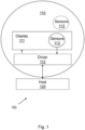
- FIG. 1 depicts a block diagram of an augmented reality system 100 in which a contact lens system 110 according to embodiments herein may be implemented.
- the augmented reality system 100 comprises a contact lens system 110 for placing in an eye and a host 120 that sends information and interacts with the contact lens system 110.
- the contact lens system 110 comprises a display 111 comprising a matrix of display elements, a driver unit 112 configured to receive data from the remote host 120 and to present the data on the display 111, a set of sensors 113 for measuring the pupil size.
- the set of sensors 113 may be integrated on the display 111.
- the driver unit 112 controls what is outputted on the display 111 and handles the input from the set of sensors 113.
- the Host 120 interacts with the contact lens system 110 via the driver unit 112.
- the display 111 with the matrix of display elements is positioned on the contact lens and is able to emit light in a structured way.
- the contact lens system may comprise a pair of contact lenses, one lens for each eye of the user.
- the lenses may be identical and display the same or different data.
- the set of sensors 113 may be photodiodes that measures the light reflected from the eye.
- Other types of pupil size or diameter sensors may also be used.
- the set of sensors may be a single- or multi-turn coil antenna. Such an antenna may receive electromagnetic radiation from the eye as the muscles controlling the iris contract and relax. It is well-known in the relevant art that muscle and neural activity of the eye may be detected through changes in electromagnetic emissions, for example with contact electrodes, capacitive sensors, and antennas. In this manner, a pupil diameter sensor based on a muscle sensor may be implemented.
- the pupil diameter sensor may also be implemented as one or more contact- or capacitive electrodes designed to measure impedance across the eye.
- Impedance may be used to detect changes in pupil diameter.
- the impedance measured across the iris and pupil may change appreciably depending on pupil diameter.
- a pupil diameter sensor placed at the appropriate location on the eye and properly coupled to the eye could detect these changes in impedance and hence the pupil diameter or size.
- not all of these sensors can be incorporated into the display. Some of these may be placed outside the display, as shown in Figure 1 sensors 113 with dotted line.
- the display 111 may have at least two display sizes defined by a matrix with different numbers of rows and columns of the display elements. Each display size is herein referred to as a valid active area setting of the display. So an active area of the display may be adjusted to have different sizes, where the numbers of rows and columns of the display elements which are active for different display sizes are different.
- the display elements may herein also be referred to as pixels.
- the amount of available display sizes varies from minimum of two, i.e. minimum and maximum, and up to the number of pixels on the diagonal of the display divided by two, if all pixel row-column interceptions have a sensor. But there is no reason of having a smaller active area than the smallest pupil dimension. Normally the pupil ranges from 2mm-8mm in diameter.
- the display 111 and its active areas may be in different shapes, where a rectangular shape and a round shape are most common for a contact lens.
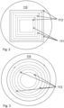
- Figure 2 shows one example of a contact lens 110 with different display sizes in rectangular shapes and a set of sensors 113.
- the set of sensors may be positioned diagonally in a corner within the display 111 at an edge of each display size.
- the set of photo sensors may be any format that is supported by the display 111.
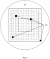
- Figure 3 shows another example of a contact lens 110 with different display sizes in a concentric pixel arrangement and a set of sensors 113. As shown in Figure 3 , the set of sensors may be positioned at different places within the display at an edge of each display size.
- the sensors 113 shown in Figures 2 and 3 may be photo sensors. Each photo sensor is designed to look into the eye and are shielded from light coming from the outside, thus only activated by light that is reflected in the eye. Measurements are performed when the display elements or pixels are in off state to avoid crosstalk the measurement from the display.
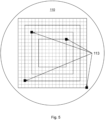
- the set of photo sensors may be positioned at intersections of the rows and columns of the display elements matrix, as shown in Figure 4 . That is, they may be positioned by each sensor replacing one or more display elements or pixels. Then the places occupied by the sensors will appear as dead pixels.
- the photo sensors may be distributed in different arrangements, as long as they are in an intersection of a row and column, for example in the corners of each display size.
- the driver unit 112 is further configured to read outputs from the set of sensors 113 to determine the pupil size and adjust a size of an active area of the display 111 based on the pupil size by activating and deactivating the display elements.
- the contact lens system 110 may further comprise one or more IR diodes placed close to a sensor to provide light towards the eye to reflect.
- the contact lens system 110 comprises a display 111 comprising a matrix of display elements, a driver unit 112 configured to receive data from a host 120 and to present the data on the display 111 and a set of sensors 113 integrated on the display 111 for measuring pupil size.
- the method comprises the following actions, which actions may be performed in any suitable order.
- the driver unit 112 Before each new frame to be presented on the display 111 or at regular intervals, e.g. every tenth frame, a few times per second or every second, the driver unit 112 checks the set of sensors 113 in order to detect the pupil size. Even if the processing and reading of the sensor signals only consume low power, a less frequent check will save some power.
- the driver unit 112 reads outputs from the set of sensors 113.
- the photo sensors are directed into the eye to be able to distinguish the edge between the pupil and the iris. Depending on the distance between the photo sensors and the number of photo sensors, the response curves when reading out the photo sensors will differ. See description of Figure 9 below.
- the light from the display elements may be used as the light source for reflectance measurements, i.e. in dark environments. This is to get the best possible signal to noise ration (SNR) to be able to find a threshold for the reflected light for the set of sensors.
- SNR signal to noise ration
- the driver unit 112 may activate the relevant display elements to provide light towards the eye to reflect.
- the display elements surrounding one photo sensor may be lighted up and the reflected rays from the display elements will be measured by the photo diode.
- the display elements outside the current pupil size should be activated to be able to find the edge. Further the display elements outside the current active area of the display may also be activated to provide light.
- the driver unit 112 may activate the relevant display elements one at a time or all at once, i.e. the relevant display elements may be flashed quickly at once or may be activated one by one in a sweeping manner.
- one or more infrared (IR) diodes may be placed close to a sensor to provide light towards the eye to reflect.
- One or several additional IR diodes may be placed next to or close to any one or all of the photo sensors. The direction of the light should be towards the eye.
- the reflected IR rays from the IR diodes are measured instead. The benefit is that it results a more stable measurement as it is not dependent on enough light from the surroundings.
- the down part is if at least one more pixel area for the display is exchanged for an IR diode, this leaves less space for pixels on the display.
- the driver unit 112 determines the pupil size based on the outputs from the set of sensors.
- sensors at various distances from the center of the iris will detect different amounts of reflected light. For example, when the iris is dilated most of the sensors may detect little light because of the large, dark pupil. Conversely, when the iris is constricted most sensors may detect higher light because of reflection of the iris.
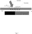
- Figure 7 shows a simplified mechanism how to use photo diodes to detect the pupil size.
- the driver unit 112 may detect the edge between the pupil and iris by comparing the detected light from the set of sensors. In the pupil area, there is almost no light reflection, so photo diodes 701, 702 will not detect any reflected light and no output signal. Photo diodes 703, 704, 705... will detect reflected light and have output signal. By comparing the detected light from the set of photo diodes 701, 702, 703, 704... the edge between the pupil and iris may be found and the display size is selected based on this.
- the driver unit 112 may determine the size of pupil by comparing the reflected light with a threshold.
- the granularity of the sensors is predefined or configured, i.e. the position, the distance between each sensor and how many sensors per area. The number of photo sensors that get reflected light enough to have an output signal over the threshold is counted and from that the pupil size is decided and the display size is selected based on this.
- the difference in signal level from the photo sensors will be dependent on whether the light that is reflected by the iris or by the inner area surrounded by the iris, i.e. the pupil, with hardly any reflection. Differences may also arise with an iris of different color and resulting different reflectance at different areas of the iris and between different users.
- the threshold should be adjusted or calibration may be needed to take account these variations.
- the threshold for reflected light may be adjusted depending on the reflectance or brightness of the iris.
- a calibration process may be implemented where the host 120 or the driver unit 112 may control the light output of the contact lens display 111.
- the gain of the photo sensors may also be controlled to find a suitable level of sensitivity. If no edge is detected between the pupil and iris, threshold can be lowered, while if multiple edges are detected, threshold can be increased.
- Photo sensors on a Low-temperature polycrystalline silicon (LTPS) substrate may be used which have the wavelength sensitivity as shown in Figure 8 , according to the article of W.J. Chiang et.al., "Silicon nanocrystal-based photosensor on low-temperature polycrystalline-silicon panels", Applied Physics Letter, 91, 051120, 2007 .
- Figure 8 shows light absorption spectrum of samples with silicon nanocrystal layers of 100, 200, and 300 nm thickness monochromatically illuminated by a constant optical power of 35 W/cm 2 and a bias voltage of 2.5 V.
- Other substrates that can be used may be Amorphous Silicon (A-Si), Indium Gallium Zinc Oxide (IGZO) or similar technologies.
- the driver unit 112 determines if the pupil size is the same as from the previous measurement. If the pupil has not changed size, the driver unit 112 will check and read outputs from the set of sensors 113 again. If the pupil has changed size, the driver unit 112 will adjust the size of an active area of the display based on the pupil size by activating and deactivating the display elements.
- the active area of the display may need to be decided and adjusted. That is appropriate number of rows and columns of the display elements may be activated based on the pupil size. Depending on the number of photo sensors placed in the display 111, the precision of the active area size will differ.
- Figure 9 shows an example of activation curves where 3, 6 and 18 photo sensors are used, where the y axis is the pupil size ranging from 2mm to 8mm, and the x axis is the number of photo sensors included in the set of sensors within the active area that ranges from 2mm to 8mm, indicated as the amount of possible display sizes. It can be seen from Figure 9 , that less photo sensors will give a jagged activation curve, i.e. when using fewer photo sensors, the adjusting of the display active area will have larger discrete steps.
- the driver unit 112 may send the size of the active area of the display to the host 120.
- the driver unit 112 either transmits the new display size to the host 120 or the host 120 asks if there is a new size and retrieves the new size from registers in the driver unit 112.
- the host 120 then adjusts its internal display buffers and settings so that a correct size of image is sent to the driver unit 112 in the contact lens 110. If the host can adjust the image size, power will be saved in the whole system 100 as the image reduction is done already on the host.
- the driver unit 112 may always receive the same size of image and depending on the active area size that is decided based on the photo sensors, the driver unit 112 will reduce the size of the image accordingly. This is a more flexible solution which will give the host 120 more freedom. The amount of data handled in the host 120 and that is transferred to the driver unit 112 is the same (maximum) size independent on the active area size of the display, thus consuming more power.
- the driver unit 112 may be configured to adjust frame buffer size of an image received from a host based on the size of active area of the display.
- the maximum lumen out of the display should always be the same independent on how many active display elements.
- the size of the virtual objects is important to consider. Displaying large virtual objects might produce lots of lumens, while displaying short texts and bounding boxes might require less. Therefore the maximum lumen output should depend on that too.
- the defined lumen value may be a preferred value or automatic adjusted according to likings of individual users. This is done to have a more comfortable usage and the user should experience the same light intensity to the retina.
- the contact lens system 110 and method therein according to the embodiments herein provide an improved visual system for augmented reality systems with at least the following advantages: Eye-mounted displays bring significant advantages in comparison to non-eye-mounted displays.
- contact lenses could be promising as wearable displays, since they are naturally discrete, and the form factor is widely accepted. Moreover, the amount of energy required to drive the displays would be significantly less than displays that are farther away.
- the display By measuring the pupil size, the display can dynamically be changed in size so that maximum amount of pixels can be used to display content.
- the user will always be able to see the maximum size of the display and that the data needed is dynamically adjusted based on the active display size.
- the system always provides a display with maximum field of view, regardless of changes to the pupil size, and without wasting power on pixels that are outside the field of view.
- the system saves power by reducing the display size and turn off pixels in the periphery, which would not be able to be seen anyway since they would be out of the field of view of the eye.
- the display size can get larger again to fill the field of view.
- the system increases the user experience by maintaining perceived brightness of the display constant or at a preferred/comfortable level by adjusting the display luminance based on the display size. This can also be seen as an optimization on power usage.
- the contact lens system itself includes all needed hardware to accomplish this.
Landscapes
- Physics & Mathematics (AREA)
- General Physics & Mathematics (AREA)
- Engineering & Computer Science (AREA)
- Optics & Photonics (AREA)
- Health & Medical Sciences (AREA)
- Ophthalmology & Optometry (AREA)
- Theoretical Computer Science (AREA)
- General Engineering & Computer Science (AREA)
- General Health & Medical Sciences (AREA)
- Human Computer Interaction (AREA)
- Computer Hardware Design (AREA)
- Devices For Indicating Variable Information By Combining Individual Elements (AREA)
- Eye Examination Apparatus (AREA)
- Control Of Indicators Other Than Cathode Ray Tubes (AREA)
- Eyeglasses (AREA)
- Controls And Circuits For Display Device (AREA)
- User Interface Of Digital Computer (AREA)
- Position Input By Displaying (AREA)
- Facsimile Scanning Arrangements (AREA)
- Lens Barrels (AREA)
- Tumbler Switches (AREA)
Priority Applications (2)
| Application Number | Priority Date | Filing Date | Title |
|---|---|---|---|
| EP22190788.4A EP4113196B1 (en) | 2019-03-26 | 2019-03-26 | A contact lens |
| ES22190788T ES3008016T3 (en) | 2019-03-26 | 2019-03-26 | A contact lens |
Applications Claiming Priority (3)
| Application Number | Priority Date | Filing Date | Title |
|---|---|---|---|
| EP22190788.4A EP4113196B1 (en) | 2019-03-26 | 2019-03-26 | A contact lens |
| EP19714592.3A EP3948404B1 (en) | 2019-03-26 | 2019-03-26 | A contact lens system |
| PCT/EP2019/057621 WO2020192898A1 (en) | 2019-03-26 | 2019-03-26 | A contact lens system |
Related Parent Applications (2)
| Application Number | Title | Priority Date | Filing Date |
|---|---|---|---|
| EP19714592.3A Division EP3948404B1 (en) | 2019-03-26 | 2019-03-26 | A contact lens system |
| EP19714592.3A Division-Into EP3948404B1 (en) | 2019-03-26 | 2019-03-26 | A contact lens system |
Publications (3)
| Publication Number | Publication Date |
|---|---|
| EP4113196A1 EP4113196A1 (en) | 2023-01-04 |
| EP4113196B1 true EP4113196B1 (en) | 2025-01-22 |
| EP4113196C0 EP4113196C0 (en) | 2025-01-22 |
Family
ID=65995700
Family Applications (2)
| Application Number | Title | Priority Date | Filing Date |
|---|---|---|---|
| EP22190788.4A Active EP4113196B1 (en) | 2019-03-26 | 2019-03-26 | A contact lens |
| EP19714592.3A Active EP3948404B1 (en) | 2019-03-26 | 2019-03-26 | A contact lens system |
Family Applications After (1)
| Application Number | Title | Priority Date | Filing Date |
|---|---|---|---|
| EP19714592.3A Active EP3948404B1 (en) | 2019-03-26 | 2019-03-26 | A contact lens system |
Country Status (16)
| Country | Link |
|---|---|
| US (3) | US11467412B2 (https=) |
| EP (2) | EP4113196B1 (https=) |
| JP (1) | JP7250949B2 (https=) |
| KR (1) | KR102600390B1 (https=) |
| CN (2) | CN116880067A (https=) |
| AU (1) | AU2019437415B2 (https=) |
| BR (1) | BR112021018710B1 (https=) |
| CO (1) | CO2021012634A2 (https=) |
| ES (2) | ES2930923T3 (https=) |
| MX (1) | MX2021011452A (https=) |
| MY (1) | MY207188A (https=) |
| PH (1) | PH12021552119A1 (https=) |
| PL (1) | PL3948404T3 (https=) |
| SG (1) | SG11202109178QA (https=) |
| WO (1) | WO2020192898A1 (https=) |
| ZA (1) | ZA202106102B (https=) |
Families Citing this family (6)
| Publication number | Priority date | Publication date | Assignee | Title |
|---|---|---|---|---|
| PH12021552119A1 (en) * | 2019-03-26 | 2022-07-11 | Ericsson Telefon Ab L M | A contact lens system |
| EP3991013A1 (en) * | 2019-06-28 | 2022-05-04 | Sony Group Corporation | Method, computer program and head-mounted device for triggering an action, method and computer program for a computing device and computing device |
| US12164109B2 (en) * | 2022-04-29 | 2024-12-10 | Snap Inc. | AR/VR enabled contact lens |
| WO2024005677A1 (en) * | 2022-06-28 | 2024-01-04 | Telefonaktiebolaget Lm Ericsson (Publ) | Methods and means for determining pupil size |
| WO2024160338A1 (en) | 2023-01-30 | 2024-08-08 | Telefonaktiebolaget Lm Ericsson (Publ) | A method for adjusting light through a smart lens |
| CN121420276A (zh) * | 2023-07-10 | 2026-01-27 | 克斯潘塞奥自然科学研究单一成员有限责任公司 | 增强现实界面控制系统和方法 |
Family Cites Families (20)
| Publication number | Priority date | Publication date | Assignee | Title |
|---|---|---|---|---|
| AR045370A1 (es) * | 2003-08-15 | 2005-10-26 | E Vision Llc | Sistema de lente electro-activo |
| CN100528070C (zh) * | 2004-09-15 | 2009-08-19 | 松下电工株式会社 | 视野计 |
| MX2009008829A (es) * | 2007-02-23 | 2011-10-28 | Pixeloptics Inc | Apertura dinamica oftalmica. |
| US20090015785A1 (en) * | 2007-06-08 | 2009-01-15 | Blum Ronald D | Adjustable correction for a variety of ambient lighting conditions |
| WO2009094587A1 (en) | 2008-01-23 | 2009-07-30 | Deering Michael F | Eye mounted displays |
| DE102009035409B4 (de) | 2009-07-31 | 2013-06-06 | Globalfoundries Dresden Module One Llc & Co. Kg | Leckstromsteuerung in Feldeffekttransistoren auf der Grundlage einer Implantationssorte, die lokal an der STI-Kante eingeführt wird |
| US20130261744A1 (en) | 2010-06-01 | 2013-10-03 | Elenza, Inc. | Implantable ophthalmic device with an aspheric lens |
| RU2013102532A (ru) | 2010-06-20 | 2014-07-27 | Эленза, Инк. | Офтальмологические устройства и способы со специализированными интегральными схемами |
| CN103596522A (zh) | 2011-03-08 | 2014-02-19 | E-视觉智能光学公司 | 先进的电活性光学装置 |
| US9219901B2 (en) | 2012-06-19 | 2015-12-22 | Qualcomm Incorporated | Reactive user interface for head-mounted display |
| US9468372B2 (en) | 2013-02-28 | 2016-10-18 | Johnson & Johnson Vision Care, Inc. | Electronic ophthalmic lens with rear-facing pupil diameter sensor |
| US9993335B2 (en) | 2014-01-08 | 2018-06-12 | Spy Eye, Llc | Variable resolution eye mounted displays |
| US9836122B2 (en) | 2014-01-21 | 2017-12-05 | Osterhout Group, Inc. | Eye glint imaging in see-through computer display systems |
| US10845620B2 (en) * | 2014-12-08 | 2020-11-24 | Aleksandr Shtukater | Smart contact lens |
| US10162412B2 (en) | 2015-03-27 | 2018-12-25 | Seiko Epson Corporation | Display, control method of display, and program |
| JP6779984B2 (ja) * | 2015-09-05 | 2020-11-04 | レイア、インコーポレイテッドLeia Inc. | 集光型バックライトおよびそれを使用するニアアイディスプレイシステム |
| US20170285370A1 (en) * | 2016-03-29 | 2017-10-05 | Intel Corporation | Automatic false pupil contact lens |
| KR101870810B1 (ko) * | 2016-11-14 | 2018-06-25 | 울산과학기술원 | 신축성 하이브리드 기판을 포함한 스마트 콘택트 렌즈 및 이의 제조방법 |
| PH12021552119A1 (en) * | 2019-03-26 | 2022-07-11 | Ericsson Telefon Ab L M | A contact lens system |
| CN115428092A (zh) * | 2019-12-30 | 2022-12-02 | 西拉格国际有限责任公司 | 用于辅助行为改变程序中的个体的系统和方法 |
-
2019
- 2019-03-26 PH PH1/2021/552119A patent/PH12021552119A1/en unknown
- 2019-03-26 BR BR112021018710-3A patent/BR112021018710B1/pt active IP Right Grant
- 2019-03-26 SG SG11202109178QA patent/SG11202109178QA/en unknown
- 2019-03-26 ES ES19714592T patent/ES2930923T3/es active Active
- 2019-03-26 KR KR1020217032989A patent/KR102600390B1/ko active Active
- 2019-03-26 CN CN202310778989.8A patent/CN116880067A/zh active Pending
- 2019-03-26 MX MX2021011452A patent/MX2021011452A/es unknown
- 2019-03-26 AU AU2019437415A patent/AU2019437415B2/en active Active
- 2019-03-26 EP EP22190788.4A patent/EP4113196B1/en active Active
- 2019-03-26 WO PCT/EP2019/057621 patent/WO2020192898A1/en not_active Ceased
- 2019-03-26 CN CN201980094460.6A patent/CN113614621B/zh active Active
- 2019-03-26 ES ES22190788T patent/ES3008016T3/es active Active
- 2019-03-26 EP EP19714592.3A patent/EP3948404B1/en active Active
- 2019-03-26 US US17/598,073 patent/US11467412B2/en active Active
- 2019-03-26 MY MYPI2021005538A patent/MY207188A/en unknown
- 2019-03-26 PL PL19714592.3T patent/PL3948404T3/pl unknown
- 2019-03-26 JP JP2021556706A patent/JP7250949B2/ja active Active
-
2021
- 2021-08-24 ZA ZA2021/06102A patent/ZA202106102B/en unknown
- 2021-09-27 CO CONC2021/0012634A patent/CO2021012634A2/es unknown
-
2022
- 2022-08-23 US US17/893,263 patent/US11726334B2/en active Active
-
2023
- 2023-06-30 US US18/217,263 patent/US12085720B2/en active Active
Also Published As
| Publication number | Publication date |
|---|---|
| US12085720B2 (en) | 2024-09-10 |
| ZA202106102B (en) | 2023-05-31 |
| EP3948404A1 (en) | 2022-02-09 |
| JP2022526142A (ja) | 2022-05-23 |
| MX2021011452A (es) | 2021-10-13 |
| MY207188A (en) | 2025-02-05 |
| PH12021552119A1 (en) | 2022-07-11 |
| SG11202109178QA (en) | 2021-09-29 |
| BR112021018710A2 (https=) | 2021-11-23 |
| CN113614621B (zh) | 2023-06-02 |
| CN116880067A (zh) | 2023-10-13 |
| KR20210136118A (ko) | 2021-11-16 |
| KR102600390B1 (ko) | 2023-11-08 |
| WO2020192898A1 (en) | 2020-10-01 |
| US11726334B2 (en) | 2023-08-15 |
| AU2019437415A1 (en) | 2021-10-07 |
| ES2930923T3 (es) | 2022-12-22 |
| US11467412B2 (en) | 2022-10-11 |
| BR112021018710B1 (pt) | 2022-07-12 |
| US20220404625A1 (en) | 2022-12-22 |
| US20220187607A1 (en) | 2022-06-16 |
| CO2021012634A2 (es) | 2021-10-20 |
| US20240004201A1 (en) | 2024-01-04 |
| JP7250949B2 (ja) | 2023-04-03 |
| CN113614621A (zh) | 2021-11-05 |
| ES3008016T3 (en) | 2025-03-21 |
| PL3948404T3 (pl) | 2023-02-06 |
| EP3948404B1 (en) | 2022-09-28 |
| AU2019437415B2 (en) | 2022-09-29 |
| EP4113196C0 (en) | 2025-01-22 |
| EP4113196A1 (en) | 2023-01-04 |
Similar Documents
| Publication | Publication Date | Title |
|---|---|---|
| US12085720B2 (en) | Contact lens system | |
| US8441422B2 (en) | Light sensitive display with object detection calibration | |
| US9411470B2 (en) | Light sensitive display with multiple data set object detection | |
| EP3200183A1 (en) | Integrated light sensitive liquid-crystal display | |
| US20080062156A1 (en) | Light sensitive display | |
| Abileah et al. | 59.3: Integrated Optical Touch Panel in a 14.1 ″AMLCD | |
| JP2010097608A (ja) | 液晶ディスプレイ装置およびその駆動方法 | |
| WO2003071345A1 (en) | Light sensitive display | |
| Abileah et al. | Optical sensors embedded within AMLCD panel: design and applications | |
| OA20513A (en) | A contact lens system | |
| HK40061161A (en) | A contact lens system | |
| US20120105379A1 (en) | Coordinate recognition apparatus and coordinate recognition method |
Legal Events
| Date | Code | Title | Description |
|---|---|---|---|
| PUAI | Public reference made under article 153(3) epc to a published international application that has entered the european phase |
Free format text: ORIGINAL CODE: 0009012 |
|
| STAA | Information on the status of an ep patent application or granted ep patent |
Free format text: STATUS: THE APPLICATION HAS BEEN PUBLISHED |
|
| AC | Divisional application: reference to earlier application |
Ref document number: 3948404 Country of ref document: EP Kind code of ref document: P |
|
| AK | Designated contracting states |
Kind code of ref document: A1 Designated state(s): AL AT BE BG CH CY CZ DE DK EE ES FI FR GB GR HR HU IE IS IT LI LT LU LV MC MK MT NL NO PL PT RO RS SE SI SK SM TR |
|
| STAA | Information on the status of an ep patent application or granted ep patent |
Free format text: STATUS: REQUEST FOR EXAMINATION WAS MADE |
|
| 17P | Request for examination filed |
Effective date: 20230612 |
|
| RBV | Designated contracting states (corrected) |
Designated state(s): AL AT BE BG CH CY CZ DE DK EE ES FI FR GB GR HR HU IE IS IT LI LT LU LV MC MK MT NL NO PL PT RO RS SE SI SK SM TR |
|
| RIC1 | Information provided on ipc code assigned before grant |
Ipc: G02B 27/01 20060101ALI20240731BHEP Ipc: G02C 7/04 20060101AFI20240731BHEP |
|
| GRAP | Despatch of communication of intention to grant a patent |
Free format text: ORIGINAL CODE: EPIDOSNIGR1 |
|
| STAA | Information on the status of an ep patent application or granted ep patent |
Free format text: STATUS: GRANT OF PATENT IS INTENDED |
|
| INTG | Intention to grant announced |
Effective date: 20240912 |
|
| GRAS | Grant fee paid |
Free format text: ORIGINAL CODE: EPIDOSNIGR3 |
|
| GRAA | (expected) grant |
Free format text: ORIGINAL CODE: 0009210 |
|
| STAA | Information on the status of an ep patent application or granted ep patent |
Free format text: STATUS: THE PATENT HAS BEEN GRANTED |
|
| AC | Divisional application: reference to earlier application |
Ref document number: 3948404 Country of ref document: EP Kind code of ref document: P |
|
| AK | Designated contracting states |
Kind code of ref document: B1 Designated state(s): AL AT BE BG CH CY CZ DE DK EE ES FI FR GB GR HR HU IE IS IT LI LT LU LV MC MK MT NL NO PL PT RO RS SE SI SK SM TR |
|
| REG | Reference to a national code |
Ref country code: GB Ref legal event code: FG4D |
|
| REG | Reference to a national code |
Ref country code: CH Ref legal event code: EP |
|
| REG | Reference to a national code |
Ref country code: IE Ref legal event code: FG4D |
|
| REG | Reference to a national code |
Ref country code: DE Ref legal event code: R096 Ref document number: 602019065308 Country of ref document: DE |
|
| U01 | Request for unitary effect filed |
Effective date: 20250122 |
|
| U07 | Unitary effect registered |
Designated state(s): AT BE BG DE DK EE FI FR IT LT LU LV MT NL PT RO SE SI Effective date: 20250128 |
|
| REG | Reference to a national code |
Ref country code: ES Ref legal event code: FG2A Ref document number: 3008016 Country of ref document: ES Kind code of ref document: T3 Effective date: 20250321 |
|
| U20 | Renewal fee for the european patent with unitary effect paid |
Year of fee payment: 7 Effective date: 20250327 |
|
| PG25 | Lapsed in a contracting state [announced via postgrant information from national office to epo] |
Ref country code: RS Free format text: LAPSE BECAUSE OF FAILURE TO SUBMIT A TRANSLATION OF THE DESCRIPTION OR TO PAY THE FEE WITHIN THE PRESCRIBED TIME-LIMIT Effective date: 20250422 |
|
| PG25 | Lapsed in a contracting state [announced via postgrant information from national office to epo] |
Ref country code: PL Free format text: LAPSE BECAUSE OF FAILURE TO SUBMIT A TRANSLATION OF THE DESCRIPTION OR TO PAY THE FEE WITHIN THE PRESCRIBED TIME-LIMIT Effective date: 20250122 |
|
| PGFP | Annual fee paid to national office [announced via postgrant information from national office to epo] |
Ref country code: ES Payment date: 20250401 Year of fee payment: 7 |
|
| PG25 | Lapsed in a contracting state [announced via postgrant information from national office to epo] |
Ref country code: IS Free format text: LAPSE BECAUSE OF FAILURE TO SUBMIT A TRANSLATION OF THE DESCRIPTION OR TO PAY THE FEE WITHIN THE PRESCRIBED TIME-LIMIT Effective date: 20250522 Ref country code: NO Free format text: LAPSE BECAUSE OF FAILURE TO SUBMIT A TRANSLATION OF THE DESCRIPTION OR TO PAY THE FEE WITHIN THE PRESCRIBED TIME-LIMIT Effective date: 20250422 |
|
| PG25 | Lapsed in a contracting state [announced via postgrant information from national office to epo] |
Ref country code: HR Free format text: LAPSE BECAUSE OF FAILURE TO SUBMIT A TRANSLATION OF THE DESCRIPTION OR TO PAY THE FEE WITHIN THE PRESCRIBED TIME-LIMIT Effective date: 20250122 |
|
| PG25 | Lapsed in a contracting state [announced via postgrant information from national office to epo] |
Ref country code: GR Free format text: LAPSE BECAUSE OF FAILURE TO SUBMIT A TRANSLATION OF THE DESCRIPTION OR TO PAY THE FEE WITHIN THE PRESCRIBED TIME-LIMIT Effective date: 20250423 |
|
| PG25 | Lapsed in a contracting state [announced via postgrant information from national office to epo] |
Ref country code: SM Free format text: LAPSE BECAUSE OF FAILURE TO SUBMIT A TRANSLATION OF THE DESCRIPTION OR TO PAY THE FEE WITHIN THE PRESCRIBED TIME-LIMIT Effective date: 20250122 |
|
| PG25 | Lapsed in a contracting state [announced via postgrant information from national office to epo] |
Ref country code: MC Free format text: LAPSE BECAUSE OF FAILURE TO SUBMIT A TRANSLATION OF THE DESCRIPTION OR TO PAY THE FEE WITHIN THE PRESCRIBED TIME-LIMIT Effective date: 20250122 |
|
| PG25 | Lapsed in a contracting state [announced via postgrant information from national office to epo] |
Ref country code: CZ Free format text: LAPSE BECAUSE OF FAILURE TO SUBMIT A TRANSLATION OF THE DESCRIPTION OR TO PAY THE FEE WITHIN THE PRESCRIBED TIME-LIMIT Effective date: 20250122 |
|
| REG | Reference to a national code |
Ref country code: CH Ref legal event code: H13 Free format text: ST27 STATUS EVENT CODE: U-0-0-H10-H13 (AS PROVIDED BY THE NATIONAL OFFICE) Effective date: 20251023 |
|
| PG25 | Lapsed in a contracting state [announced via postgrant information from national office to epo] |
Ref country code: SK Free format text: LAPSE BECAUSE OF FAILURE TO SUBMIT A TRANSLATION OF THE DESCRIPTION OR TO PAY THE FEE WITHIN THE PRESCRIBED TIME-LIMIT Effective date: 20250122 |
|
| PLBE | No opposition filed within time limit |
Free format text: ORIGINAL CODE: 0009261 |
|
| STAA | Information on the status of an ep patent application or granted ep patent |
Free format text: STATUS: NO OPPOSITION FILED WITHIN TIME LIMIT |
|
| 26N | No opposition filed |
Effective date: 20251023 |
|
| PG25 | Lapsed in a contracting state [announced via postgrant information from national office to epo] |
Ref country code: CH Free format text: LAPSE BECAUSE OF NON-PAYMENT OF DUE FEES Effective date: 20250331 |
|
| PG25 | Lapsed in a contracting state [announced via postgrant information from national office to epo] |
Ref country code: IE Free format text: LAPSE BECAUSE OF NON-PAYMENT OF DUE FEES Effective date: 20250326 |
|
| PGFP | Annual fee paid to national office [announced via postgrant information from national office to epo] |
Ref country code: GB Payment date: 20260327 Year of fee payment: 8 |