EP4099577A1 - System and method of clock recovery with low phase-error for card emulation clock-less nfc transceivers - Google Patents
System and method of clock recovery with low phase-error for card emulation clock-less nfc transceivers Download PDFInfo
- Publication number
- EP4099577A1 EP4099577A1 EP21290036.9A EP21290036A EP4099577A1 EP 4099577 A1 EP4099577 A1 EP 4099577A1 EP 21290036 A EP21290036 A EP 21290036A EP 4099577 A1 EP4099577 A1 EP 4099577A1
- Authority
- EP
- European Patent Office
- Prior art keywords
- signal
- card
- phase error
- phase
- nfc
- Prior art date
- Legal status (The legal status is an assumption and is not a legal conclusion. Google has not performed a legal analysis and makes no representation as to the accuracy of the status listed.)
- Pending
Links
- 238000011084 recovery Methods 0.000 title claims abstract description 101
- 238000000034 method Methods 0.000 title claims description 59
- 230000005540 biological transmission Effects 0.000 claims abstract description 96
- 238000005070 sampling Methods 0.000 claims abstract description 48
- 238000012937 correction Methods 0.000 claims abstract description 32
- 238000004891 communication Methods 0.000 claims description 31
- 230000004913 activation Effects 0.000 claims description 13
- 239000013078 crystal Substances 0.000 claims description 13
- 238000004590 computer program Methods 0.000 claims description 6
- 230000003534 oscillatory effect Effects 0.000 claims description 6
- 238000003860 storage Methods 0.000 claims description 4
- 238000001914 filtration Methods 0.000 claims description 3
- 238000012545 processing Methods 0.000 claims description 3
- 230000001276 controlling effect Effects 0.000 description 25
- 230000003446 memory effect Effects 0.000 description 20
- 238000010586 diagram Methods 0.000 description 13
- 230000008878 coupling Effects 0.000 description 11
- 238000010168 coupling process Methods 0.000 description 11
- 238000005859 coupling reaction Methods 0.000 description 11
- 238000012935 Averaging Methods 0.000 description 6
- 230000007704 transition Effects 0.000 description 4
- 238000013461 design Methods 0.000 description 3
- 230000001965 increasing effect Effects 0.000 description 3
- 230000000737 periodic effect Effects 0.000 description 3
- 230000000694 effects Effects 0.000 description 2
- 230000001939 inductive effect Effects 0.000 description 2
- 230000001105 regulatory effect Effects 0.000 description 2
- 230000008054 signal transmission Effects 0.000 description 2
- 239000010752 BS 2869 Class D Substances 0.000 description 1
- 238000013016 damping Methods 0.000 description 1
- 238000004519 manufacturing process Methods 0.000 description 1
- 239000000203 mixture Substances 0.000 description 1
- 238000005457 optimization Methods 0.000 description 1
- 230000010355 oscillation Effects 0.000 description 1
- 230000035945 sensitivity Effects 0.000 description 1
- 230000001360 synchronised effect Effects 0.000 description 1
Images


Classifications
-
- H—ELECTRICITY
- H03—ELECTRONIC CIRCUITRY
- H03L—AUTOMATIC CONTROL, STARTING, SYNCHRONISATION, OR STABILISATION OF GENERATORS OF ELECTRONIC OSCILLATIONS OR PULSES
- H03L7/00—Automatic control of frequency or phase; Synchronisation
- H03L7/06—Automatic control of frequency or phase; Synchronisation using a reference signal applied to a frequency- or phase-locked loop
- H03L7/08—Details of the phase-locked loop
- H03L7/081—Details of the phase-locked loop provided with an additional controlled phase shifter
- H03L7/0812—Details of the phase-locked loop provided with an additional controlled phase shifter and where no voltage or current controlled oscillator is used
- H03L7/0814—Details of the phase-locked loop provided with an additional controlled phase shifter and where no voltage or current controlled oscillator is used the phase shifting device being digitally controlled
-
- H04B5/72—
-
- H—ELECTRICITY
- H04—ELECTRIC COMMUNICATION TECHNIQUE
- H04L—TRANSMISSION OF DIGITAL INFORMATION, e.g. TELEGRAPHIC COMMUNICATION
- H04L7/00—Arrangements for synchronising receiver with transmitter
- H04L7/02—Speed or phase control by the received code signals, the signals containing no special synchronisation information
- H04L7/033—Speed or phase control by the received code signals, the signals containing no special synchronisation information using the transitions of the received signal to control the phase of the synchronising-signal-generating means, e.g. using a phase-locked loop
- H04L7/0337—Selecting between two or more discretely delayed clocks or selecting between two or more discretely delayed received code signals
-
- G—PHYSICS
- G06—COMPUTING; CALCULATING OR COUNTING
- G06K—GRAPHICAL DATA READING; PRESENTATION OF DATA; RECORD CARRIERS; HANDLING RECORD CARRIERS
- G06K7/00—Methods or arrangements for sensing record carriers, e.g. for reading patterns
- G06K7/10—Methods or arrangements for sensing record carriers, e.g. for reading patterns by electromagnetic radiation, e.g. optical sensing; by corpuscular radiation
- G06K7/10009—Methods or arrangements for sensing record carriers, e.g. for reading patterns by electromagnetic radiation, e.g. optical sensing; by corpuscular radiation sensing by radiation using wavelengths larger than 0.1 mm, e.g. radio-waves or microwaves
- G06K7/10297—Methods or arrangements for sensing record carriers, e.g. for reading patterns by electromagnetic radiation, e.g. optical sensing; by corpuscular radiation sensing by radiation using wavelengths larger than 0.1 mm, e.g. radio-waves or microwaves arrangements for handling protocols designed for non-contact record carriers such as RFIDs NFCs, e.g. ISO/IEC 14443 and 18092
-
- H—ELECTRICITY
- H03—ELECTRONIC CIRCUITRY
- H03L—AUTOMATIC CONTROL, STARTING, SYNCHRONISATION, OR STABILISATION OF GENERATORS OF ELECTRONIC OSCILLATIONS OR PULSES
- H03L7/00—Automatic control of frequency or phase; Synchronisation
- H03L7/06—Automatic control of frequency or phase; Synchronisation using a reference signal applied to a frequency- or phase-locked loop
- H03L7/08—Details of the phase-locked loop
- H03L7/0807—Details of the phase-locked loop concerning mainly a recovery circuit for the reference signal
-
- H—ELECTRICITY
- H03—ELECTRONIC CIRCUITRY
- H03L—AUTOMATIC CONTROL, STARTING, SYNCHRONISATION, OR STABILISATION OF GENERATORS OF ELECTRONIC OSCILLATIONS OR PULSES
- H03L7/00—Automatic control of frequency or phase; Synchronisation
- H03L7/06—Automatic control of frequency or phase; Synchronisation using a reference signal applied to a frequency- or phase-locked loop
- H03L7/08—Details of the phase-locked loop
- H03L7/085—Details of the phase-locked loop concerning mainly the frequency- or phase-detection arrangement including the filtering or amplification of its output signal
- H03L7/093—Details of the phase-locked loop concerning mainly the frequency- or phase-detection arrangement including the filtering or amplification of its output signal using special filtering or amplification characteristics in the loop
-
- H—ELECTRICITY
- H03—ELECTRONIC CIRCUITRY
- H03L—AUTOMATIC CONTROL, STARTING, SYNCHRONISATION, OR STABILISATION OF GENERATORS OF ELECTRONIC OSCILLATIONS OR PULSES
- H03L7/00—Automatic control of frequency or phase; Synchronisation
- H03L7/06—Automatic control of frequency or phase; Synchronisation using a reference signal applied to a frequency- or phase-locked loop
- H03L7/08—Details of the phase-locked loop
- H03L7/099—Details of the phase-locked loop concerning mainly the controlled oscillator of the loop
- H03L7/0991—Details of the phase-locked loop concerning mainly the controlled oscillator of the loop the oscillator being a digital oscillator, e.g. composed of a fixed oscillator followed by a variable frequency divider
-
- H—ELECTRICITY
- H04—ELECTRIC COMMUNICATION TECHNIQUE
- H04B—TRANSMISSION
- H04B1/00—Details of transmission systems, not covered by a single one of groups H04B3/00 - H04B13/00; Details of transmission systems not characterised by the medium used for transmission
- H04B1/38—Transceivers, i.e. devices in which transmitter and receiver form a structural unit and in which at least one part is used for functions of transmitting and receiving
- H04B1/40—Circuits
-
- H04B5/48—
-
- H—ELECTRICITY
- H04—ELECTRIC COMMUNICATION TECHNIQUE
- H04L—TRANSMISSION OF DIGITAL INFORMATION, e.g. TELEGRAPHIC COMMUNICATION
- H04L7/00—Arrangements for synchronising receiver with transmitter
- H04L7/0016—Arrangements for synchronising receiver with transmitter correction of synchronization errors
- H04L7/0033—Correction by delay
-
- H—ELECTRICITY
- H04—ELECTRIC COMMUNICATION TECHNIQUE
- H04L—TRANSMISSION OF DIGITAL INFORMATION, e.g. TELEGRAPHIC COMMUNICATION
- H04L7/00—Arrangements for synchronising receiver with transmitter
- H04L7/02—Speed or phase control by the received code signals, the signals containing no special synchronisation information
- H04L7/033—Speed or phase control by the received code signals, the signals containing no special synchronisation information using the transitions of the received signal to control the phase of the synchronising-signal-generating means, e.g. using a phase-locked loop
-
- H—ELECTRICITY
- H04—ELECTRIC COMMUNICATION TECHNIQUE
- H04L—TRANSMISSION OF DIGITAL INFORMATION, e.g. TELEGRAPHIC COMMUNICATION
- H04L7/00—Arrangements for synchronising receiver with transmitter
- H04L7/04—Speed or phase control by synchronisation signals
- H04L7/041—Speed or phase control by synchronisation signals using special codes as synchronising signal
- H04L7/046—Speed or phase control by synchronisation signals using special codes as synchronising signal using a dotting sequence
Definitions
- the present disclosure relates to a card clock recovery system for use in a Near Field Communication (NFC) card transceiver; an NFC card transceiver being for use in communication with an NFC reader device and having such a card clock recovery system; a method of correcting a signal phase of a card clock generation control signal, for example in such a card clock recovery system; as well as a corresponding computer program product and a non-transitory storage medium.
- NFC Near Field Communication
- NFC Near Field Communication
- ALM Active Load Modulation
- Next generation NFC applications seek for clock-less Card Emulation ALM transceivers, i.e. transceivers which are able to reach this phase accuracy without any reference clock, that is without any crystal and/or without any external reference clock on the platform.
- a first aim is to build an extremely low-cost application for the IOT (internet of things) market and/or for the wearable market.
- a second aim is to be able to perform Card Emulation in so-called "phone off' modes of applications: when the battery is nearly fully depleted, all system clocks are switched off to preserve battery charge as much as possible.
- the card transceiver shall be capable to keep its phase locked to the reader field signal not only during a receiving mode of operation, but also during a transmission mode of operation, that is to say when the card transmitter corrupts the reader phase information, to which a card clock recovery system intends to lock on.
- an NFC card clock recovery system it is a general object of the present disclosure for an NFC card clock recovery system to be enabled to accurately lock on the reader signal phase, not only during a receiving mode of operation, but even during a card transmission mode of operation.
- a card clock recovery system for use in a Near Field Communication (NFC) card transceiver, wherein the NFC card transceiver is couplable to an NFC reader, and wherein the card clock recovery system has a phase lock loop having: (1) a phase/frequency detector (PFD), which is configured to receive a reference signal provided at an RX port of a matching network during a receiving mode of the NFC transceiver or to receive a reference signal provided at the RX port of the matching network during a transmission mode of the NFC transceiver, to receive, via a loop feedback line, a loop feedback signal, and to provide a phase error signal that represents a phase difference between the reference signal and the loop feedback signal; (2) a loop filter configured to receive a corrected phase error signal that is derived from the phase error signal, and to provide a filtered corrected phase error signal; and (3) a controllable oscillator, CO, which is configured to receive the filtered corrected phase error signal (for example as
- the phase offset correction unit has: (a) a phase error sampling unit, which is configured to receive the phase error signal, to sample one or more phase error signals at one or more first and at one or more second discrete points in time, and to provide one or more sampled phase error signals sampled at the one or more first and the one or more second discrete points in time; (b) a phase offset computation unit, which is configured to receive the one or more sampled phase error signals sampled at the one or more first and at the one or more second discrete points in time, to compute a phase offset signal that corresponds to a difference between at least one sampled phase error signal sampled at a second discrete point in time and at least one sampled phase error signal sampled at a first discrete point in time, and to provide the phase offset signal; and (c) a phase subtractor unit, which is configured to receive the phase error signal provided by the PFD, to receive the phase offset signal provided by the phase offset computation unit, to subtract the phase error signal from the phase offset signal to
- the phase offset computation unit is configured (i) to store a plurality of first phase error signals sampled at plural first discrete points in time, to compute a first average out of these stored first phase error signals sampled at plural first discrete points in time, and to store the first average; (ii) to store a plurality of second phase error signals sampled at plural second discrete points in time, to compute a second average out of these stored second phase error signals sampled at plural second discrete points in time, and to store the second average; and (iii) to compute a difference between the second average and the first average, and to provide this difference as the phase offset signal, for example to the phase subtracter unit.
- the phase offset computation unit further has (d) a phase offset finite state machine, which is configured to output: (I) a first state control signal to be received by the phase error sampling unit for controlling (a) the timing of the one or more first discrete points in time and (b) the timing of the one or more second discrete points in time; (II) a second state control signal to be received by the phase offset computation unit for (c) controlling the timing of the storing of the one or more first phase error signals sampled at the one or more first discrete points in time, and for example the computing of the first average out of these stored first phase error signals, for (d) controlling the timing of the storing of the one or more second phase error signals sampled at the one or more second discrete points in time, and for example the computing of the second average out of these stored second phase error signals, and for (c) controlling the timing of the computing of the difference between the second average and the first average; and (III) a third state control signal to be received by the loop filter for controlling
- the phase offset finite state machine has: (i) a first control signal input configured to receive a first control signal that controls an activation of a card transmitter driver; (ii) a second control signal input configured to receive a second control signal that controls an activation period of the modulation of the card transmitter driver for generating a modulated output voltage signal that represents an encoded symbol to be transmitted by the card transmitter; and (iii) a third control signal input configured to receive a third control signal that controls the timing of the sampling of the one or more first phase error signals sampled at the one or more first discrete points in time, and for example the computing of the first average of these stored first phase error signals, and the timing of the sampling of the one or more second phase error signals sampled at the one or more second discrete points in time, and for example the computing of the second average of these stored second phase error signals.
- the system further has (iv) a fourth control signal, which corresponds to the third state control signal and is to be received by the loop filter for controlling the control input of the controlled oscillator, wherein the control input of the controlled oscillator is frozen when the fourth control signal is set to be TRUE.
- the one or more first discrete points in time are while the card transceiver operates in a receiving mode, or while the card transceiver receives a continuous wave, CW, emission from an NFC reader, to which the NFC transceiver is coupled, during a transmission mode of the card transceiver; and the one or more second discrete points in time are while the card transceiver operates in a transmitting mode and towards the ends of respective symbol transmission periods.
- the system has at least one of the following features:
- an NFC card transceiver for use in communication with an NFC reader, wherein the NFC transceiver has a card antenna, a card matching network, a card receiver, a card transmission controller, a card transmission driver, a card clock recovery system according to the first aspect of the present disclosure, and a card clock generation unit.
- the card matching network is coupled to the card antenna, is configured to output a receiver, RX, input signal at an RX port of the matching network, which RX input signal is generated during a receiving mode of the NFC transceiver, for example while the NFC transceiver receives a continuous wave, CW, emission from an NFC reader, to receive a transmission, TX, output signal at a TX port of the matching network, which TX output signal is generated during a transmission mode of the NFC transceiver.
- the card receiver is configured to receive the RX input provided at the RX port of the matching network, and to receive a receiver clock signal from the card clock generation unit.
- the card transmission controller is configured to output a card transmission control signal.
- the card transmission driver is configured to receive the card transmission control signal, to receive a transmission clock signal, and to provide the TX output signal to the TX port of the card matching network.
- the card clock recovery system is configured to either receive the RX input signal provided at the RX port during a receiving mode of the NFC transceiver or to receive the RX input signal during a transmission mode of the NFC transceiver, and to provide a card clock generation control signal to the card clock generation unit.
- the card clock generation unit is configured to receive the card clock generation control signal from the card clock recovery system, to provide the receiver clock signal to the card receiver, and to provide the transmission clock signal to the card transmission driver.
- the NFC transceiver is one of a clock-less transceiver, or an NFC transceiver does not have a reference clock unit or an oscillatory crystal.
- a method for correcting a signal phase of a card clock generation control signal which is generated as an output of a card clock recovery system of an NFC transceiver and is configured for being received by a card clock generation unit of an NFC transceiver.
- the card clock recovery system has a phase/frequency detector, PFD, a loop filter, a controllable oscillator, CO, and a phase offset correction unit.
- the method has: (i) receiving, at a reference input of the PFD, a reference input signal; (ii) receiving, at a feedback input of the PFD, a loop feedback signal; (iii) generating, at an output of the PFD, a phase error signal that represents a phase difference between the reference signal and the loop feedback signal; (iv) generating, by the phase offset correction unit, a phase offset signal and subtracting the phase error signal from the phase offset signal so as to thereby provide a corrected phase error signal; (v) receiving, by the loop filter, the corrected phase error signal, filtering, in the loop filter, the corrected phase error signal so as to provide a filtered corrected phase error signal; (vi) receiving, by the controllable oscillator, the filtered corrected phase error signal, commanding therewith the controllable oscillator so as to provide, by the controlled oscillator, a controlled frequency output signal; (vii) providing the controlled frequency output signal as the loop feedback signal to the PFD; and (viii) providing the controlled frequency output signal as the
- the phase offset correction unit of the NFC transceiver further has a phase error sampling unit, a phase offset computation unit, and a phase subtractor unit.
- generating the phase offset signal further comprises: sampling the phase error signal, by the phase error sampling unit, at one or more first discrete points in time and at one or more second discrete points in time; computing, by the phase offset computation unit, a phase offset signal that is obtained as a difference between a phase error signal sampled at a second discrete point in time and a phase error signal sampled at a first discrete point in time; and subtracting, by the phase subtracter unit, the phase error signal from the phase offset signal so as to thereby provide the corrected phase error signal, to the loop filter.
- the method further has, in the phase offset computation unit: (i) storing a plurality of first phase error signals sampled at plural first discrete points in time, computing a first average out of these stored first phase error signals sampled at plural first discrete points in time, and storing the first average; (ii) storing a plurality of second phase error signals sampled at plural second discrete points in time, computing a second average out of these stored second phase error signals sampled at plural second discrete points in time, and storing the second average; and (iii) computing a difference between the second average and the first average, and providing this difference as the phase offset signal, to the phase subtractor unit.
- the phase offset correction unit further has a phase offset finite state machine.
- the method further has: (1) providing, by the phase offset finite state machine, a first state control signal to the phase error sampling unit for (a) controlling the timing of the one or more first discrete points in time and (b) the timing of the one or more second discrete points in time; (II) providing, by the phase offset finite state machine, a second state control signal to the phase offset computation unit for (c) controlling the timing of the storing of the first phase error signals sampled at the one or more first discrete points in time, and for example the computing of the first average out of these stored first phase error signals, for (d) controlling the timing of the storing of the one or more second phase error signals sampled at the one or more second discrete points in time, and for example the computing of the second average out of these stored second phase error signals, and for (e) controlling the timing of the computing of the difference between the second phase error signal and the first phase error signal, or for example the difference between the second phase error signal and the first phase error
- the method further has, in the phase offset finite state machine: (i) receiving, for example at a first control signal input of the finite state machine, a first control signal that controls an activation of a card transmitter driver; (ii) receiving, for example at a second control signal input of the finite state machine, a second control signal that controls an activation period of the modulation of the card transmitter driver for generating a modulated output voltage signal that represents an encoded symbol to be transmitted by the card transmitter; and (iii) receiving, for example at a third control signal input of the finite state machine, a third control signal that controls the timing of the sampling of the one or more first phase error signals sampled at one or more first discrete points in time, and for example the computing of the first average of these stored first phase error signals, and the timing of the sampling of the one or more second phase error signals sampled at one or more second discrete points in time, and for example the computing of the second average of these stored second phase error signals.
- the method further has controlling the control input of the CO by a fourth control signal, which corresponds to the third state control signal and is be received by the loop filter, wherein the control input is frozen when the fourth control signal is set to be TRUE.
- the one or more first discrete points in time are while the card transceiver operates in a receiving mode, or while the card transceiver receives a continuous wave, CW, emission from an NFC reader, to which the NFC transceiver is coupled, during a transmission mode of the card transceiver; and the one or more second discrete points in time are while the card transceiver operates in a transmission mode and towards the ends of respective symbol transmission periods.
- a machine-readable, non-transitional storage medium storing a computer program product, or a computer program product, which comprises instructions, which when executed on a data processing system, such as a processor, a micro-processor, or a computer, control or execute the method according to the third aspect of the present disclosure.
- ALM Active Load Modulation
- Fig. 1 shows a schematic block diagram of a conventional NFC communication system 100 having an NFC reader 110 and an NFC card transceiver 150, which has a reference clock 190 and/or an oscillatory crystal.
- the NFC reader 110 in a conventional design has a reader system 120 that issues and receives requests and data, a reader matching network 130 that transforms signals representing requests and data as used by the reader system 120 to radio frequency (RF) signals that can be transmitted to or received from the reader antenna 140.
- RF radio frequency
- the NFC card transceiver 150 in a conventional design has a card transceiver 160 that is capable to operate in a receiving (RX) mode and in a transmitting (TX) mode for receiving and transmitting data, a card matching network 170 that transforms signals representing data as used by the card transceiver 160 to RF signals that can be transmitted to or received from the card antenna 180.
- a magnetic coupling represented in Fig.
- the digital circuits in the card transceiver 160 are conventionally synchronized by clock signals provided a reference clock 190 and/or an oscillatory crystal 190, and may further have a card clock recovery system for recovering a clock signal from a periodic signal received via the card antenna 180 and through the card matching network 170.
- the wide deployment of NFC applications requests highly integrated, cost-effective new clock recovery techniques.
- the present disclosure describes a system and a method allowing to improve the performance of clock recovery systems in that they result in a reduced phase error, without necessity of any clock or crystal in the application.
- Fig. 2 shows a schematic block diagram of a NFC communication system 200 having a conventional NFC reader 110 (as in Fig. 1 ) and a clock-less NFC card transceiver 250.
- the clock-less NFC card transceiver 250 of Fig. 2 has a card antenna 180 and a card matching network 170 like those in the conventional NFC card transceiver 150 of Fig. 1 , while the card transceiver 260 of Fig. 2 differs from the card transceiver 160 of Fig. 1 in that the card transceiver 260 does not have any clock or crystal, i.e.
- Next generation NFC applications seek for ALM clock-less transceivers, like the card transceiver 260 of Fig. 2 , which are capable to achieve the required phase accuracy without any reference clock, i.e. neither a crystal nor a reference clock available on the platform.
- Such design allows (i) to build extremely low-cost applications for the internet of things (IOT) market and/or the wearable market, and/or (ii) to be able to perform Card Emulation in so-called "phone-off" modes of operation, i.e. when the battery is nearly fully depleted, all system clocks are switched off to preserve battery charge.
- a two-way communication can be established between the NFC reader 110 and the NFC card transceiver 150.
- Such two-way communication proceeds according to established standards, for example ISO 14443.
- Fig. 3 shows a communication example involving an NFC reader 110 as a proximity coupling device (PCD) and an NFC transceiver 160, 260 as a proximity inductive coupling card. (PICC), according to ISO14443.
- the communication for a typical transaction has started in that the NFC reader 110 assumes a transmission (TX) state and sends an unmodulated periodic signal to produce by the reader antenna 140 an unmodulated periodic magnetic field, i.e. a continuous wave (CW) transmission 320, while the card transceiver 160, 260 is in a standby state 360.
- TX transmission
- CW continuous wave
- the NFC reader 110 proceeds and sends data frames destined for the NFC card transceiver 1 60, 260, in the format of PCD-to-PICC frames 325, which will cause the NFC card transceiver 160, 260 to answer to the NFC reader 110. Accordingly, the NFC reader 110 stops transmitting PCD-to-PICC frames 325 and starts to wait for the NFC transceiver 160, 260 to answer.
- the NFC transceiver 160, 260 answers by starting to transmit data frames destined for the NFC reader 110, in the format of PICC-to-PCD frames 365, while the NFC reader 110 is in a state of continuous wave (CW) transmission 330. It is noted that the NFC reader 110 is in the state of CW transmission 330 before the NFC card transceiver 160, 260 starts transmitting PICC-to-PCD frames 365, and also until after the NFC card transceiver 160, 260 has stopped transmitting PICC-to-PCD frames 365.
- CW continuous wave
- the NFC transceiver 160, 260 returns to a standby state 370, and the NFC reader 110 stops its CW transmission 330 and resumes transmitting PCD-to-PICC frames 335, while the NFC transceiver 160, 260 listens and remains in its standby state 370.
- a frame (PCD-to-PICC, or PICC-to-PCD) can be as long as 20 ms, and a full transaction can last a few seconds.
- the duration of a PICC-to-PCD frame 365 forces the clock-less NFC card transceiver 250 to perform clock recovery during this PICC-to-PCD frame 365 in order to ensure an accurate phase synchronization with the NFC reader 110.
- EP 2 988 427 A1 discloses a method for a phase calibration in a frontend circuit of an NFC tag device.
- the present disclosure provides a solution for a card clock recovery system in an NFC card transceiver 260 (see Fig. 2 ), 450 (see Fig. 4 ), in particular for a Card Emulation ALM transceiver, to accurately lock on a phase of a signal 330 (see Fig. 3 ) of an NFC reader 110, 410, even during a card transmission mode of operation.
- the novel system and method of clock recovery according to this disclosure is embedded in a card clock recovery system 480 (see Fig. 4 ) and 500 (see Fig. 5 ) as shown in Fig. 7 .
- the novel card clock recovery system 480, 500 as shown in Fig. 7 is embedded in a phase lock loop (PLL) 505, such as the PLL 505 shown in Fig. 5 , which locks in the phase and the frequency of an NFC reader 410.
- PLL phase lock loop
- the context for operation of the novel card clock recovery system 480, 500 is shown in Fig. 4 .
- Fig. 4 shows a schematic block diagram of an NFC communication system 400 having an NFC reader 410 and a clock-less NFC card transceiver 450 having a card clock recovery system 480 according to an exemplary embodiment of the present disclosure.
- the NFC reader 410 is the master, and as such provides a 13,56 MHz magnetic field (CW signal 330 as shown in Figs. 3 and 6 ) through the reader matching network 435 and through the reader antenna 440. Via the magnetic coupling k (see Fig. 4 ), this signal enters the NFC transceiver 450 via the card antenna 490 and the card matching network 475 (see the RX signal 476 in Fig. 4 ), and arrives as the RX input signal 472 at the card receiver (RX) 470 and at an input of the card clock recovery system 480.
- CW signal 330 as shown in Figs. 3 and 6
- this signal enters the NFC transceiver 450 via the card antenna 490 and the card matching network 475 (see the RX signal 476 in Fig. 4 ), and arrives as the RX input signal 472 at the card receiver (RX) 470 and at an input of the card clock recovery system 480.
- the card clock recovery system 480 locks to the frequency and phase of the incoming field (CW signal 330), thereby defines the reference clocks for the card transceiver 450, and provides an according card clock generation control signal 482 to a card clock generation unit 485. The latter in turn provides the proper receiver clock signal 486 to the card RX 470 and the proper card transmission clock signal 487 to the card transmission (TX) driver 465.
- the card clock recovery system 480 might provide multiple high-frequency reference clock signals, i.e. 8 phases at 650 MHz.
- the TX clock generation (as a part of the card clock generation unit 485) includes according frequency dividers and digital logic to build PWM signals from the high-frequency clocks.
- the RX clock generation (as another part of the card clock generation unit 485) might include frequency dividers from 7,8 GHz down to 13,56 MHz to a few hundreds MHz.
- the card clock recovery system 480, 500 is based on a phase lock loop (PLL) 505 and has: a phase/frequency detector (PFD) 510, a loop filter 520, a controllable oscillator 530, and a feedback line 536 comprising an optional feedback divider 540.
- PLL phase lock loop
- PFD phase/frequency detector
- Fig. 5 shows a schematic block diagram of a card clock recovery system 500, which forms the basis for the novel card clock recovery system according to an exemplary embodiment of the present disclosure (as shown in Fig. 7 ).
- the PLL 505 locks the phase of its internal controllable oscillator 530 to the CW field signal 330 of the NFC reader 410 by sensing the RX input signal 472 from time to time during the receiving mode of operation of the NFC transceiver 450.
- the PFD 510 compares the phase of the internal oscillator 520 (feedback signal 538), optionally divided by the feedback divider 540, with the phase of the reader field, CW signal 330 (reference signal 512), and generates an output signal 518 that is indicative of a phase difference, also called phase error, between the loop feedback signal 538 and the reference signal 512.
- the phase error signal 518 is integrated in the loop filter 520, which outputs a filtered phase error signal 526 that commands (or controls) the internal oscillator 530.
- the controllable oscillator 530 may be embodied as a digitally controlled oscillator (DCO), or as a voltage-controlled oscillator (VCO).
- DCO digitally controlled oscillator
- VCO voltage-controlled oscillator
- the circuit representation of the so-operating PLL 505 is shown in Fig. 5
- an associated chronogram with signals and control signals is shown in Fig. 6 .
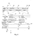
- Fig. 6 shows a schematic chronogram of a conventional card clock recovery method, wherein a phase error ( ⁇ at 635) of the clock recovery principle is increasing from one TX burst to the next ( ⁇ at 635, 2* ⁇ at 635', ...) due to the matching network memory effect, hence leading to a divergence of the clock recovery.
- the card clock recovery system 500 locks ideally to the reader phase during the reader unmodulated (CW) field emission 330, but fails to maintain this accurate phase when the card transmitter 460, 465 is transmitting. This is due to the corruption of the phase of the card antenna 490 by the NFC transceiver's 450 own transmitter 460, 465 during the card transmission, and because of the relatively high quality factor (Q ⁇ 8-12) of the card antenna.
- the voltage and phase at the card antenna 490 during TX transmission bursts 615, after the end of a TX burst, need time to converge back to the voltage and phase corresponding to the reader unmodulated (CW) field emission 330.
- this time may not be sufficient so that a remainder ⁇ (see at 635 in Fig. 6 ) of the phase error at the card antenna 490 remains after a first TX burst and cannot converge back fully after the TX burst. Then, after a second TX burst, there remains a remainder 2* ⁇ (see at 635' in Fig. 6 ) of the phase error at the card antenna 490, and so on.
- this effect is referred to as the matching network memory effect of the card matching network 475.
- This matching network memory effect prevents the clock recovery to sample accurately the reader phase ( ⁇ Reader).
- the clock recovery samples, at the points 660 in time, a mixture of the reader phase ( ⁇ reader) and the card transmitter phase ( ⁇ CardTX), which leads to an overall phase that is equal to ⁇ Reader + ⁇ (see Fig. 6 ).
- This effect can even result in a de-lock (or divergence) of the PLL 505 (possibly causing to wrong phase, a wrong frequency of card clock recovery, see Fig. 6 during the points 660 in time), which may lead to a non-functional system.
- the matching network memory effect gets even worse, when the NFC communication system 400 operates near sensitivity, when the card transceiver 450 transmits its maximum power to the reader 410, and the reader signal, as perceived at the card antenna 490, is the weakest. Then, the perceived phase at the card antenna 490 is the most polluted by the card's 450 own transmitter 460, 465.
- the teaching of the present disclosure aims to correct and/or compensate the card transmitter phase for the matching network memory effect during card transmission operations, and thereby make it possible to maintain a small phase error even during the transmission phase of a card transceiver and to improve the performance of a card clock recovery system in respect of the matching network memory effect.
- a card clock recovery system 500 comprises a PLL (phase locked loop) 505 having a phase/frequency detector (PFD) 510, a loop filter 520, a controllable oscillator 530 (e.g. DCO or VCO), and an optional feedback divider 540, and in addition a phase offset correction unit 700 coupled in the PLL 505 between the PFD 510 and the loop filter 520.
- PFD phase/frequency detector
- a controllable oscillator 530 e.g. DCO or VCO
- optional feedback divider 540 optional feedback divider 540
- the phase offset correction unit 700 operates as follows:
- Fig. 4 shows a schematic block diagram of an NFC communication system 400 having an NFC reader 410 and a clock-less NFC card transceiver 450 having a card clock recovery system 480, 500 according to an exemplary embodiment of the present disclosure.
- Fig. 4 shows the system context, in which the teaching of the present disclosure is implemented.
- the teaching of the present disclosure is implemented in a card clock recovery system 480 (as shown in Fig. 4 ) or 500 (as shown in Fig. 7 ), which is employed in a clock-less NFC card transceiver 250, 450 of an NFC communication system 200, 400.
- the NFC transceiver 450 may be a clock-less transceiver (see 250 in Fig. 2 ).
- the NFC transceiver 450 may be an NFC transceiver 250, 450 that does not have a reference clock unit 190 or an oscillatory crystal 190 (see Fig. 1 ).
- the NFC card transceiver 150, 450 is intended to be used in communication with an NFC reader 110, 410.
- the NFC transceiver 450 has a card antenna 490, a card matching network 475, a card receiver 470, a card transmission controller 460, a card transmission driver 465, a card clock recovery system 480 (see also 500 in Fig. 7 ) according to an embodiment example of the present disclosure, and a card clock generation unit 485.
- the card matching network 475 is coupled to the card antenna 490, and is configured to output an RX output 476 corresponding to a matching network output generated during a receiving mode of the NFC transceiver 450, for example while the NFC transceiver 450 receives a continuous wave, CW, emission 320, 330, 340 from an NFC reader 410, as a receiver input, RX, signal 472.
- the card matching network 475 is further configured to receive a transmission driver output, TX, signal 467, and to provide a matching network output signal 477 generated during a transmission mode of the NFC transceiver.
- the card receiver 470 is configured to receive the RX output 476 provided by the card matching network 475, and to receive a receiver clock signal 486 from the card clock generation unit 485.
- the card transmission controller 460 is configured to output a card transmission control signal 462,
- the card transmission driver 465 is configured to receive the card transmission control signal 462, to receive a transmission clock signal 487, and to provide a TX driver output signal 467 to the card matching network 475.
- the card clock recovery system 480 (see 500 in Fig. 7 ) is configured to either receive the RX signal 472 during a receiving mode of the NFC transceiver 450 or to receive the matching network output signal 477 during a transmission mode of the NFC transceiver 450, and to provide a card clock generation control signal 482 to the card clock generation unit 485.
- the card clock generation unit 485 is configured to receive the card clock generation control signal 482 from the card clock recovery system 480 (see 500 in Fig. 7 ), to provide the receiver clock signal 486 to the card receiver 470, and to provide the transmission clock signal 487 to the card transmission driver 465.
- Fig. 7 shows a schematic block diagram of a card clock recovery system 480, 500, which has a phase offset correction unit 700 that is capable to remove the matching network memory effect, according to the present disclosure.
- a card clock recovery system 500 (see also 480 in Fig. 4 ) is intended for use in an NFC card transceiver 450 (see also 250 in Fig. 2 ).
- the NFC card transceiver 450 is couplable to an NFC reader 410 (see also 110 in Fig. 1 ), to thereby form an NFC communication system 400.
- the card clock recovery system 500 has a phase lock loop (505) having: a phase/frequency detector (PFD) 510, a loop filter 520, a controllable oscillator (CO) 530, and furthermore a phase offset correction unit 700 according to an embodiment example of the present disclosure.
- PFD phase/frequency detector
- CO controllable oscillator
- the phase/frequency detector (PFD) 510 is configured to receive a reference signal 512 provided at an RX port 476 of a matching network 475 during a receiving mode of the NFC transceiver 450 or to receive a reference signal provided at the RX port 476 of the matching network 475 during a transmission mode of the NFC transceiver 450.
- the PDF 510 is further configured to receive, via a loop feedback line 536, a loop feedback signal 538, and to provide, at its phase error output 516, a phase error signal 518.
- the latter (phase error signal 518) represents a phase difference between the reference signal 512 and the loop feedback signal 538.
- the loop filter 520 is configured to receive a corrected phase error signal 722 that is derived from the phase error signal 518, and to provide a filtered phase error signal 526.
- the loop filter 520 is configured to integrate, over time, the received corrected phase error signal 722 to thereby generate the provided filtered corrected phase error signal 526.
- the controllable oscillator (CO) 530 is configured to receive the filtered corrected phase error signal 526, as a commanding control input signal, and to provide a controlled frequency output signal 534.
- the latter i.e. the controlled frequency output signal 534, is provided as the card clock generation control signal 539 to the card clock generation unit 485 of the NFC card transceiver 450, and as the loop feedback signal 538, via the loop feedback line 536, to the PFD 510 as its feedback input.
- the controllable oscillator 530 may be implemented as a digitally controlled oscillator (DCO) or as a voltage controlled oscillator (VCO).
- the phase lock loop 505 further may have, a feedback divider 540 provided in the loop feedback line 536.
- the feedback divider 540 may be configured to divide the frequency of the loop feedback signal 538.
- the card clock recovery system 500 further has a phase offset correction unit 700.
- the phase offset correction unit 700 is configured to receive the phase error signal 518 provided by the PFD 510 and to provide the corrected phase error signal 756 to the loop filter 520.
- the phase offset correction unit 700 has at least: a phase error sampling unit 720, a phase offset computation unit 730, and a phase subtractor unit 740.
- the phase error sampling unit 720 is configured to receive the phase error signal 518, 722, to sample one or more phase error signals 722 at one or more first 655 and at one or more second 665 discrete points in time, and to provide one or more sampled phase error signals 724 sampled at the one or more first 655 and the one or more second 665 discrete points in time.
- the phase offset computation unit 730 is configured to receive the one or more sampled phase error signals 724 sampled at the one or more first discrete points 655 in time and at the one or more second discrete points 665 in time, to compute a phase offset signal 734 that corresponds to a difference between at least one sampled phase error signal sampled at a second discrete point 665 in time and at least one sampled phase error signal sampled at a first discrete point 655 in time, and to provide the phase offset signal 734.
- the one or more first discrete points 655 in time (indicated in the signal traces 630 in Fig. 6 and 830 in Fig. 8 ) arc while the NFC card transceiver 450 operates in a receiving mode, or while the card transceiver 450 receives a continuous wave, CW, emission 330 from an NFC reader 110; 410, to which the NFC transceiver 450 is coupled, during a transmission mode of the card transceiver.
- the one or more second discrete points 660 in time (also indicated in the signal traces 630 in Fig. 6 and 830 in Fig. 8 ) are while the NFC card transceiver 450 operates in a transmitting mode and towards the ends of respective symbol transmission periods 617.
- the phase subtractor unit 740 is configured to receive the phase error signal 518, 722 provided by the PFD 510, to receive the phase offset signal 734 provided by the phase offset computation unit 730, to subtract the phase error signal 722 from the phase offset signal 734 to thereby generate the corrected phase error signal 746, and to provide the corrected phase error signal 746, namely to the loop filter 520.
- the phase offset computation unit 730 may be configured (i) to store a plurality of first phase error signals sampled at plural first discrete points 650 in time, to compute a first average ( ⁇ 0, avg ), out of these stored first phase error signals sampled at plural first discrete points 655 in time, and to store the first average ( ⁇ 0, avg ).
- the phase offset computation unit 730 may further be configured (ii) to store a plurality of second phase error signals sampled at plural second discrete points 665 in time, to compute a second average, ⁇ 1, avg , out of these stored second phase error signals sampled at plural second discrete points in time, and to store the second average ⁇ 1, avg .
- the phase offset computation unit 730 further has a phase offset finite state machine 710, which is configured to output a first state control signal 711, a second state control signal 712, and a third state control signal 713.
- the first state control signal 711 is to be received by the phase error sampling unit 720 for controlling (a) the timing of the one or more first discrete points 655 in time and (b) the timing of the one or more second discrete points 665 in time.
- the second state control signal 712 is to be received by the phase offset computation unit 730 for (c) controlling the timing of the storing of the one or more first phase error signals sampled at the one or more first discrete points 655 in time, and for example the computing of the first average, ⁇ 0, avg , out of these stored first phase error signals, for (d) controlling the timing of the storing of the one or more second phase error signals sampled at the one or more second discrete points 665 in time, and for example the computing of the second average, ⁇ 1, avg , out of these stored second phase error signals, and for (c) controlling the timing of the computing of the difference, ⁇ , between the second average, ⁇ 1, avg , and the first average, ⁇ 0, avg .
- the phase offset finite state machine 710 has: a first control signal input 715, a second control signal input 716, and a third control signal input 717.
- the first control signal input 715 (see also the control signal 910, named Tx_active in Fig. 9 ) is configured to receive a first control signal 910 that controls an activation of a card transmitter driver 465.
- the second control signal input 716 (see also the control signal 920, named Tx_cnv in Fig. 9 ) is configured to receive a second control signal 920 that controls an activation period 617 of the modulation of the card transmitter driver 465 for generating a modulated output voltage signal that represents an encoded symbol 615 to be transmitted by the card transmitter 460, 465.
- the third control signal input 717 (see also the control signal 940, named TrackField) is configured to receive a third control signal 940 that controls the timing of the sampling of the one or more first phase error signals sampled at the one or more first discrete points 655 in time, and for example the computing of the first average, ⁇ 0, avg , of these stored first phase error signals, and the timing of the sampling of the one or more second phase error signals sampled at the one or more second discrete points 665 in time, and for example the computing of the second average, ⁇ 1, avg , of these stored second phase error signals.
- the third state control signal 713 (see also the control signal 980 in Fig. 9 , named Freeze_Osc) is input to the loop filter 520 and it causes a control such that the control input 532 of the CO 530 is frozen when the third state control signal 713 (i.e. the control signal 980) is set to be (or transitions from "FALSE” to) "TRUE". Later, when the phase correction has been determined and applied, i.e. when the phase offset ⁇ off has been subtracted from the phase error signal 518 output from the PFD 510, the phase lock loop 505 can track again the reference signal 472, 512, and correspondingly the control input 532 of the CO 530 can be unfrozen.
- the loop filter 520 returns to receive the corrected phase error signal 756, provides the filtered corrected phase error signal 526, and thereby commands the CO 530 to provide a controlled frequency output signal 534, which is regulated by the phase lock loop 505.
- the one or more first discrete points 655 in time are while the NFC card transceiver 450 operates in a receiving mode, or while the card transceiver 450 receives a continuous wave, CW, emission 330 from an NFC reader 110; 410, to which the NFC transceiver 450 is coupled, during a transmission mode of the card transceiver.
- the one or more second discrete points 665 in time are while the NFC card transceiver 450 operates in a transmitting mode and towards the ends of respective symbol transmission periods 617.
- Fig. 8 shows a schematic chronogram of a card clock recovery method 1000 according to the present disclosure, with removal of the matching network memory effect, wherein a phase error (see ⁇ at 635) of the clock recovery principle is compensated.
- the chronogram of Fig. 8 differs from the chronogram of Fig. 6 namely in that the trace of the signal 830 differs from the trace of the signal 630.
- the phase error at the end of a transmission burst period 617 related to the transmission of a signal 615 increases from one period 617 to the next period 617; refer in Fig. 6 to the phase error ⁇ at the end of the first symbol burst period 617. to the phase error 2* ⁇ at the end of the second symbol burst period 617, and so on in the trace 630.
- phase errors at the end of a transmission burst periods 617 related to the transmission of signals 615 docs not increase from one period 617 to the next 617. but rather remains small at ⁇ ; refer in Fig. 8 to the phase errors ⁇ in the trace 830.
- Fig. 9 shows a schematic chronogram of the control signals (see 715, 716, 717 in Fig. 7 , 910, 920, 930, 940, 980 in Fig. 9 ) used in a card clock recovery system 500 (see Fig. 7 ) according to the present disclosure, with removal of the matching network memory effect.
- Trace 910 is the trace of the first control signal 715, which is herein referred to as "Tx_active” and which is input to the phase offset finite state machine 710 as shown in Fig. 7 .
- This first control signal “Tx_active” is set during the whole period of transmission of PICC-to-PCD frames, see reference numeral 365 in the trace 350 representing the card transmission (TX) state in Figures 6 and 8 .
- "'Tx_active” is set (for example to "High") irrespective of whether the carrier signal is transmitted (as indicated by the second control signal 716 (“Tx_env”) being set in trace 920) or not ("Tx_env" not being set in trace 920).
- Trace 920 is the trace of the second control signal 716, which is herein referred to as "Tx_env” and which is input to the phase offset finite state machine 710 as shown in Fig. 7 .
- This second control signal “Tx _env” represents the modulation signal, and it is set when the carrier signal is transmitted (as indicated by the second control signal 716 (“Tx_env”) being set in trace 920).
- Trace 940 is the trace of the third control signal 717, which is herein referred to as "TrackField” and which is input to the phase offset finite state machine 710 as shown in Fig. 7 .
- This third control signal “TrackField” triggers the sampling (or acquisition) of the phase error output signal 518 provided at the output of the PFD 510.
- the control signal “TrackField” triggers the sampling of the phase error output signal 518 both over the first points 650 in time (see Figs. 6 and 8 , trace 640 "clock recovery phase sampling”) (or see at 950 in the traces 940 and 650 in Fig. 9 ), i.e.
- Trace 950 is the trace of controlling the sampling of the PFD output 518 and averaging during first points 650, 950 in time, i.e. during a receive operation of the NFC card transceiver, thereby yielding the first average ( ⁇ 0, avg ) put of the first phase error signals sampled at plural first discrete points 650, 950 in time.
- Trace 960 is the trace of controlling the sampling of the PFD output 518 and averaging during second points 660, 960 in time, i.e. during a transmission operation of the NFC card transceiver at the end of a TX transmission burst, thereby yielding the second average ( ⁇ 1, avg ) out of the second phase error signals sampled at plural second discrete points 660, 960 in time.
- Trace 970 is the trace of controlling the phase correction, when the phase offset ⁇ off is subtracted from the phase error signal 518 output from the PFD 510, as performed in the phase subtracter unit 740.
- the event of applying the phase correction i.e. subtracting the phase offset ⁇ off from the phase error signal 518 output from the PFD 510, triggers a transition of the third state control signal 713, also named Freeze_Osc, from "TRUE" to "FALSE", as explained in the following.
- Trace 980 is the trace of controlling the control input 532 of the controllable oscillator 530 using the third state control signal 713, also named Freeze_Osc, output by the phase offset finite state machine 710.
- the control of this fourth control signal 980 i.e. the third state control signal 713, Freeze_Osc
- the control input 532 of the CO 530 is frozen when the control signal 980, i.e. the third state control signal 713, Freeze_Osc, is set (or transitions from "FALSE") to "TRUE".
- the phase correction has been applied, i.e.
- the phase lock loop 505 can track again the reference signal 472, 512, and correspondingly the control input 532 of the CO 530 can be unfrozen, which is set by the third state control signal 713, Freeze_Osc, transitioning to "FALSE". Further with reference to Fig. 7 , when the third state control signal 713, Freeze_Osc, has been set back to "FALSE", the loop filter 520 returns to receive the corrected phase error signal 756, provides the filtered corrected phase error signal 526, and thereby commands the CO 530 to provide a controlled frequency output signal 534, which is regulated by the phase lock loop 505.
- Fig. 10 shows a flow diagram of a method 1000 of correcting a signal phase of a card clock generation control signal 539, with removal of the matching network memory effect, according to the present disclosure.
- the method 1000 aims to correct a signal phase of a card clock generation control signal 482, 539 for the influence of the matching network memory effect.
- the card clock generation control signal 482, 539 is generated as an output of a card clock recovery system 480, 500 of an NFC transceiver 450 and is configured for being received by a card clock generation unit 485 of the NFC transceiver 450. As shown in Fig.
- the card clock recovery system 500 has a phase/frequency detector (PFD) 510, a loop filter 520, a controlled oscillator (CO) 530, and a phase offset correction unit 700, which has a phase offset finite state machine 710, a phase error sampling unit 720, a phase offset computation unit 730, and a phase subtractor unit 740.
- PFD phase/frequency detector
- CO controlled oscillator
- the method 1000 begins at step 1010 of receiving, at a reference input of the PFD 510, a reference input signal 512.
- the method proceeds to step 1020 of receiving, at a feedback input of the PFD 510, a loop feedback signal 514.
- the method further proceeds to step 1030 of generating, at an output of the PFD 510, a phase error signal 518, 722 that represents a phase difference between the reference input signal 512 and the loop feedback signal 514.
- the steps 1010, 1020 and 1030 are performed both during the first points 650 in time, i.e. while the NFC transceiver operates in a receiving mode, and during the second points 660 in time, i.e. while the NFC transceiver operates in a transmission mode.
- the one or more first discrete points 650, 950 in time are while the NFC card transceiver 450 operates in a receiving mode and receives a continuous wave, CW, emission 330 from an NFC reader 110, 410, to which the NFC transceiver 450 is coupled.
- the one or more second discrete points 660 in time are while the NFC card transceiver 450 operates in a transmitting mode and towards the ends of respective symbol transmission periods 617.
- step 1040 of generating, by the phase offset correction unit 700, a phase offset signal 714 and subtracting the phase error signal 518, 722 from the phase offset signal 714 to thereby provide a corrected phase signal 746.
- the step 1040 comprises, and is detailed by, the steps 1041 to 1045, which are described in the following.
- the step 1040 comprises step 1041 of sampling the phase error signal 518, 722, by the phase error sampling unit 720, at one or more first discrete points 650 in time.
- Step 1040 further comprises step 1042 of storing a plurality of first phase error signals sampled at plural first discrete points 650 in time, computing a first average ( ⁇ 0, avg ) out of these stored first phase error signals sampled at plural first discrete points 650 in time, and storing the first average ( ⁇ 0, avg ).
- the method proceeds to step 1043, which is also comprised in step 1040, involving sampling the phase error signal 518, 722, by the phase error sampling unit 720, at one or more second discrete points 660 in time.
- Step 1040 further comprises step 1044 of storing a plurality of second phase error signals sampled at plural second discrete points 660 in time, computing a second average ( ⁇ 1, avg ) out of these stored second phase error signals sampled at plural second discrete points 660 in time, and storing the second average ( ⁇ 1, avg ).
- the method proceeds to the step 1045 of computing, by the phase offset computation unit 730, a phase offset signal 714 that is obtained as a difference between a phase error signal sampled at a second discrete point 660 in time and a phase error signal sampled at a first discrete point 650 in time.
- Step 1045 may also comprise computing a difference ( ⁇ ) between the second average ( ⁇ 1, avg ) and the first average ( ⁇ 0, avg ), and providing this difference as the phase offset signal ( ⁇ off), to the phase subtracter unit 740.
- the method 1000 further proceeds to step 1050 of subtracting, by the phase subtractor unit 740, the phase offset signal 714 from the phase error signal 518, 722, so as to thereby provide the corrected phase error signal 756, to the loop filter 520.
- step 1050 of subtracting, by the phase subtractor unit 740, the phase offset signal 714 from the phase error signal 518, 722, so as to thereby provide the corrected phase error signal 756, to the loop filter 520.
- step 1050 of subtracting, by the phase subtractor unit 740, the phase offset signal 714 from the phase error signal 518, 722, so as to thereby provide the corrected phase error signal 756, to the loop filter 520.
- step 1090 of providing the controlled frequency output signal 534 as the signal phase corrected card clock generation control signal 482, 539, to the card clock generation unit 485 of the NFC transceiver 450 is followed both by the step 1080 of providing the controlled frequency output signal 534 as the loop feedback signal 514, 538 to the PFD 510 (feedback signal 514), and by the step 1090 of providing the controlled frequency output signal 534 as the signal phase corrected card clock generation control signal 482, 539, to the card clock generation unit 485 of the NFC transceiver 450.
- the method 1000 further comprises steps performed in the phase offset finite state machine 710, as follows.
- the method 1000 may comprise a step of providing, by the phase offset finite state machine 710, a first state control signal 711 to the phase error sampling unit 920 for controlling (a) the timing of the one or more first discrete points 655 in time and (b) the timing of the one or more second discrete points 665 in time.
- the method may comprise a step of providing, by the phase offset finite state machine 710, a second state control signal 712 to the phase offset computation unit 730 for (c) controlling the timing of the storing of the first phase error signals sampled at the one or more first discrete points 655 in time, and for example the computing of the first average ( ⁇ 0, avg ) out of these stored first phase error signals, for (d) controlling the timing of the storing of the one or more second phase error signals sampled at the one or more second discrete points 665 in time, and for example the computing of the second average ( ⁇ 1, avg ) out of these stored second phase error signals, and for (e) controlling the timing of the computing of the difference between the second phase error signal and the first phase error signal, or for example the difference ( ⁇ ) between the second average ( ⁇ 1, avg ) and the first average ( ⁇ 0, avg ).
- the method 1000 may further comprise, in the phase offset finite state machine 710, a step of receiving, at a first control signal input 715 of the finite state machine 710, a first control signal 910 (elsewhere referred to as Tx_active) that controls an activation of a card transmitter driver 785, namely during the transmission by the NFC card transceiver 450 of all the transmitted PICC-to-PCD frames (see 365 in card Tx state 350 in Fig. 8 ).
- Tx_active a first control signal 910
- the method 1000 may comprise, in the phase offset finite state machine 710, a step of receiving, at a second control signal input 716 of the finite state machine 710, a second control signal 920 (elsewhere referred to as Tx_env) that controls an activation period 617 of the modulation of the card transmitter driver 465 for generating a modulated output voltage signal that represents an encoded symbol 615 to be transmitted by the card transmitter 460, 465.
- Tx_env a second control signal 920
- the method 1000 may comprise, in the phase offset finite state machine 710, a step of receiving, at a third control signal input 717 of the finite state machine 710, a third control signal 940 (elsewhere referred to as TrackField) that controls the timing of the sampling of the one or more first phase error signals sampled at one or more first discrete points 655 in time, and the computing of the first average ( ⁇ 0, avg ) of these stored first phase error signals, and the timing of the sampling of the one or more second phase error signals sampled at one or more second discrete points 665 in time, and the computing of the second average ( ⁇ 1, avg ) of these stored second phase error signals.
- TrackField a third control signal 940
- the method 1000 may comprise, in the phase offset finite state machine 710, a step of outputting, as a third state control signal 713 of the finite state machine 710, a control signal 980 (elsewhere referred to as Freeze_Osc), which is to be received by the loop filter 520 for controlling the control input 532 of the controllable oscillator 530 such that the control input 532 is frozen when the third state control signal 713 is set to be "TRUE".
- Freeze_Osc a control signal 980
Abstract
Description
- The present disclosure relates to a card clock recovery system for use in a Near Field Communication (NFC) card transceiver; an NFC card transceiver being for use in communication with an NFC reader device and having such a card clock recovery system; a method of correcting a signal phase of a card clock generation control signal, for example in such a card clock recovery system; as well as a corresponding computer program product and a non-transitory storage medium.
- The wide deployment of Near Field Communication (NFC) applications demands for highly integrated, cost-effective manufacturing and operation techniques, including for example effective techniques for providing clock signals. In this respect, a demand leads towards highly integrated, cost-effective new clock recovery techniques with increased performance of such systems in respect notably of reducing the phase error. This may allow to deploy NFC card or card emulation applications without any clock or oscillating crystal in the application.
- In NFC applications, a trend has been and continues towards using Active Load Modulation (ALM) transmitters, which allow to increase the NFC communication distance by about one order of magnitude and/or allow to operate with much smaller antennas. Such ALM systems with small antennas require the Card Emulation transmitter phase to be accurately locked to the phase of a reader, with a maximum phase error typically of +/-10°. If this phase accuracy is not achieved, a Card Emulation ALM transmitter cannot interoperate with many world-wide legacy readers, which operate with a single path (non-IQ) receiver.
- Next generation NFC applications seek for clock-less Card Emulation ALM transceivers, i.e. transceivers which are able to reach this phase accuracy without any reference clock, that is without any crystal and/or without any external reference clock on the platform. A first aim is to build an extremely low-cost application for the IOT (internet of things) market and/or for the wearable market. A second aim is to be able to perform Card Emulation in so-called "phone off' modes of applications: when the battery is nearly fully depleted, all system clocks are switched off to preserve battery charge as much as possible.
- There is thus a need to dispense with the provision and use of clocks and crystals, i.e. to provide clock-less systems. For an NFC card transceiver, this may require to generate a clock from a frequency reference provided by the reader. This can be achieved by phase- and frequency aligning to transitions in a magnetic field e.g. with a phase lock loop (PLL), Such a process is referred to as clock recovery.
- Then, given that in an NFC card transceiver the receiver RX and the transmitter TX share the same antenna, one of the key technical challenges to solve for clock-less Card Emulation ALM transceivers is that the card transceiver shall be capable to keep its phase locked to the reader field signal not only during a receiving mode of operation, but also during a transmission mode of operation, that is to say when the card transmitter corrupts the reader phase information, to which a card clock recovery system intends to lock on.
- It is a general object of the present disclosure for an NFC card clock recovery system to be enabled to accurately lock on the reader signal phase, not only during a receiving mode of operation, but even during a card transmission mode of operation.
- This object is solved by the subjects having the features according to the independent patent claims. In particular, these objects are solved by a card clock recovery system for use in an NFC card transceiver according to the appended
independent claim 1, an NFC card transceiver according to the appended independent claim 8, a method of correcting a signal phase of a card clock generation control signal output by an NFC card clock recovery system according to the appended independent claim 10, as well as a computer program product and a non-transitory storage medium according to the appended independent claim 16. - According to a first aspect of the present disclosure, there is provided a card clock recovery system for use in a Near Field Communication (NFC) card transceiver, wherein the NFC card transceiver is couplable to an NFC reader, and wherein the card clock recovery system has a phase lock loop having: (1) a phase/frequency detector (PFD), which is configured to receive a reference signal provided at an RX port of a matching network during a receiving mode of the NFC transceiver or to receive a reference signal provided at the RX port of the matching network during a transmission mode of the NFC transceiver, to receive, via a loop feedback line, a loop feedback signal, and to provide a phase error signal that represents a phase difference between the reference signal and the loop feedback signal; (2) a loop filter configured to receive a corrected phase error signal that is derived from the phase error signal, and to provide a filtered corrected phase error signal; and (3) a controllable oscillator, CO, which is configured to receive the filtered corrected phase error signal (for example as a commanding control input signal) and to provide a controlled frequency output signal, which is provided as the card clock generation control signal to a card clock generation unit of an NFC card transceiver, and as the loop feedback signal, via the loop feedback line, to the PFD. The card clock recovery system further has (4) a phase offset correction unit, which is configured to receive the phase error signal provided by the PFD and to provide the corrected phase error signal to the loop filter.
- In an embodiment example of the card clock recovery system, the phase offset correction unit has: (a) a phase error sampling unit, which is configured to receive the phase error signal, to sample one or more phase error signals at one or more first and at one or more second discrete points in time, and to provide one or more sampled phase error signals sampled at the one or more first and the one or more second discrete points in time; (b) a phase offset computation unit, which is configured to receive the one or more sampled phase error signals sampled at the one or more first and at the one or more second discrete points in time, to compute a phase offset signal that corresponds to a difference between at least one sampled phase error signal sampled at a second discrete point in time and at least one sampled phase error signal sampled at a first discrete point in time, and to provide the phase offset signal; and (c) a phase subtractor unit, which is configured to receive the phase error signal provided by the PFD, to receive the phase offset signal provided by the phase offset computation unit, to subtract the phase error signal from the phase offset signal to thereby generate the corrected phase error signal, and to provide the corrected phase error signal, for example to the loop filter.
- In an embodiment example of the card clock recovery system, the phase offset computation unit is configured (i) to store a plurality of first phase error signals sampled at plural first discrete points in time, to compute a first average out of these stored first phase error signals sampled at plural first discrete points in time, and to store the first average; (ii) to store a plurality of second phase error signals sampled at plural second discrete points in time, to compute a second average out of these stored second phase error signals sampled at plural second discrete points in time, and to store the second average; and (iii) to compute a difference between the second average and the first average, and to provide this difference as the phase offset signal, for example to the phase subtracter unit.
- In an embodiment example of the card clock recovery system, the phase offset computation unit further has (d) a phase offset finite state machine, which is configured to output: (I) a first state control signal to be received by the phase error sampling unit for controlling (a) the timing of the one or more first discrete points in time and (b) the timing of the one or more second discrete points in time; (II) a second state control signal to be received by the phase offset computation unit for (c) controlling the timing of the storing of the one or more first phase error signals sampled at the one or more first discrete points in time, and for example the computing of the first average out of these stored first phase error signals, for (d) controlling the timing of the storing of the one or more second phase error signals sampled at the one or more second discrete points in time, and for example the computing of the second average out of these stored second phase error signals, and for (c) controlling the timing of the computing of the difference between the second average and the first average; and (III) a third state control signal to be received by the loop filter for controlling a control input of the controlled oscillator such that the control input of the controlled oscillator is frozen when the third state control signal is set to be TRUE.
- In an embodiment example of the card clock recovery system, the phase offset finite state machine has: (i) a first control signal input configured to receive a first control signal that controls an activation of a card transmitter driver; (ii) a second control signal input configured to receive a second control signal that controls an activation period of the modulation of the card transmitter driver for generating a modulated output voltage signal that represents an encoded symbol to be transmitted by the card transmitter; and (iii) a third control signal input configured to receive a third control signal that controls the timing of the sampling of the one or more first phase error signals sampled at the one or more first discrete points in time, and for example the computing of the first average of these stored first phase error signals, and the timing of the sampling of the one or more second phase error signals sampled at the one or more second discrete points in time, and for example the computing of the second average of these stored second phase error signals.
- In an embodiment example of the card clock recovery system, the system further has (iv) a fourth control signal, which corresponds to the third state control signal and is to be received by the loop filter for controlling the control input of the controlled oscillator, wherein the control input of the controlled oscillator is frozen when the fourth control signal is set to be TRUE.
- In an embodiment example of the card clock recovery system, the one or more first discrete points in time are while the card transceiver operates in a receiving mode, or while the card transceiver receives a continuous wave, CW, emission from an NFC reader, to which the NFC transceiver is coupled, during a transmission mode of the card transceiver; and the one or more second discrete points in time are while the card transceiver operates in a transmitting mode and towards the ends of respective symbol transmission periods.
- In an embodiment example of the card clock recovery system, the system has at least one of the following features:
- (1) the controllable oscillator is one of a digitally controlled oscillator, DCO, or a voltage controlled oscillator, VCO;
- (2) the phase lock loop further has, a feedback divider provided in the loop feedback line, wherein the feedback divider is configured to divide the frequency of the loop feedback signal;
- (3) the loop filter is configured to integrate over time and/or to amplify by a proportionality factor the received corrected phase error signal so as to thereby generate the provided filtered corrected phase error signal.
- According to a second aspect of the present disclosure, there is provided an NFC card transceiver for use in communication with an NFC reader, wherein the NFC transceiver has a card antenna, a card matching network, a card receiver, a card transmission controller, a card transmission driver, a card clock recovery system according to the first aspect of the present disclosure, and a card clock generation unit. The card matching network is coupled to the card antenna, is configured to output a receiver, RX, input signal at an RX port of the matching network, which RX input signal is generated during a receiving mode of the NFC transceiver, for example while the NFC transceiver receives a continuous wave, CW, emission from an NFC reader, to receive a transmission, TX, output signal at a TX port of the matching network, which TX output signal is generated during a transmission mode of the NFC transceiver. The card receiver is configured to receive the RX input provided at the RX port of the matching network, and to receive a receiver clock signal from the card clock generation unit. The card transmission controller is configured to output a card transmission control signal. The card transmission driver is configured to receive the card transmission control signal, to receive a transmission clock signal, and to provide the TX output signal to the TX port of the card matching network. The card clock recovery system is configured to either receive the RX input signal provided at the RX port during a receiving mode of the NFC transceiver or to receive the RX input signal during a transmission mode of the NFC transceiver, and to provide a card clock generation control signal to the card clock generation unit. The card clock generation unit is configured to receive the card clock generation control signal from the card clock recovery system, to provide the receiver clock signal to the card receiver, and to provide the transmission clock signal to the card transmission driver.
- In an embodiment example of the NFC card transceiver, the NFC transceiver is one of a clock-less transceiver, or an NFC transceiver does not have a reference clock unit or an oscillatory crystal.
- According to a third aspect of the present disclosure, there is provided a method for correcting a signal phase of a card clock generation control signal, which is generated as an output of a card clock recovery system of an NFC transceiver and is configured for being received by a card clock generation unit of an NFC transceiver. Herein, the card clock recovery system has a phase/frequency detector, PFD, a loop filter, a controllable oscillator, CO, and a phase offset correction unit. The method has: (i) receiving, at a reference input of the PFD, a reference input signal; (ii) receiving, at a feedback input of the PFD, a loop feedback signal; (iii) generating, at an output of the PFD, a phase error signal that represents a phase difference between the reference signal and the loop feedback signal; (iv) generating, by the phase offset correction unit, a phase offset signal and subtracting the phase error signal from the phase offset signal so as to thereby provide a corrected phase error signal; (v) receiving, by the loop filter, the corrected phase error signal, filtering, in the loop filter, the corrected phase error signal so as to provide a filtered corrected phase error signal; (vi) receiving, by the controllable oscillator, the filtered corrected phase error signal, commanding therewith the controllable oscillator so as to provide, by the controlled oscillator, a controlled frequency output signal; (vii) providing the controlled frequency output signal as the loop feedback signal to the PFD; and (viii) providing the controlled frequency output signal as the signal phase corrected card clock generation control signal, to the card clock generation unit of the NFC transceiver.
- In an embodiment example of the method, the phase offset correction unit of the NFC transceiver further has a phase error sampling unit, a phase offset computation unit, and a phase subtractor unit. Herein, generating the phase offset signal further comprises: sampling the phase error signal, by the phase error sampling unit, at one or more first discrete points in time and at one or more second discrete points in time; computing, by the phase offset computation unit, a phase offset signal that is obtained as a difference between a phase error signal sampled at a second discrete point in time and a phase error signal sampled at a first discrete point in time; and subtracting, by the phase subtracter unit, the phase error signal from the phase offset signal so as to thereby provide the corrected phase error signal, to the loop filter.
- In an embodiment example of the method, the method further has, in the phase offset computation unit: (i) storing a plurality of first phase error signals sampled at plural first discrete points in time, computing a first average out of these stored first phase error signals sampled at plural first discrete points in time, and storing the first average; (ii) storing a plurality of second phase error signals sampled at plural second discrete points in time, computing a second average out of these stored second phase error signals sampled at plural second discrete points in time, and storing the second average; and (iii) computing a difference between the second average and the first average, and providing this difference as the phase offset signal, to the phase subtractor unit.
- In an embodiment example of the method, the phase offset correction unit further has a phase offset finite state machine. Herein, the method further has: (1) providing, by the phase offset finite state machine, a first state control signal to the phase error sampling unit for (a) controlling the timing of the one or more first discrete points in time and (b) the timing of the one or more second discrete points in time; (II) providing, by the phase offset finite state machine, a second state control signal to the phase offset computation unit for (c) controlling the timing of the storing of the first phase error signals sampled at the one or more first discrete points in time, and for example the computing of the first average out of these stored first phase error signals, for (d) controlling the timing of the storing of the one or more second phase error signals sampled at the one or more second discrete points in time, and for example the computing of the second average out of these stored second phase error signals, and for (e) controlling the timing of the computing of the difference between the second phase error signal and the first phase error signal, or for example the difference between the second average and the first average; and (III) providing, by the phase offset finite state machine, a third state control signal to be received by the loop filter for controlling a control input of the controlled oscillator such that the control input of the controlled oscillator is frozen when third state control signal is set to be TRUE.
- In an embodiment example of the method, the method further has, in the phase offset finite state machine: (i) receiving, for example at a first control signal input of the finite state machine, a first control signal that controls an activation of a card transmitter driver; (ii) receiving, for example at a second control signal input of the finite state machine, a second control signal that controls an activation period of the modulation of the card transmitter driver for generating a modulated output voltage signal that represents an encoded symbol to be transmitted by the card transmitter; and (iii) receiving, for example at a third control signal input of the finite state machine, a third control signal that controls the timing of the sampling of the one or more first phase error signals sampled at one or more first discrete points in time, and for example the computing of the first average of these stored first phase error signals, and the timing of the sampling of the one or more second phase error signals sampled at one or more second discrete points in time, and for example the computing of the second average of these stored second phase error signals.
- In an embodiment example of the method, the method further has controlling the control input of the CO by a fourth control signal, which corresponds to the third state control signal and is be received by the loop filter, wherein the control input is frozen when the fourth control signal is set to be TRUE.
- In an embodiment example of the method, the one or more first discrete points in time are while the card transceiver operates in a receiving mode, or while the card transceiver receives a continuous wave, CW, emission from an NFC reader, to which the NFC transceiver is coupled, during a transmission mode of the card transceiver; and the one or more second discrete points in time are while the card transceiver operates in a transmission mode and towards the ends of respective symbol transmission periods.
- According to a fourth aspect of the present disclosure, there is provided a machine-readable, non-transitional storage medium storing a computer program product, or a computer program product, which comprises instructions, which when executed on a data processing system, such as a processor, a micro-processor, or a computer, control or execute the method according to the third aspect of the present disclosure.
- In the following, exemplary embodiment examples of the present disclosure are described in detail with reference to the appended drawings, in which:
-
Fig. 1 shows a schematic block diagram of a conventional NFC communication system having an NFC reader and an NFC card-transceiver, which has a reference clock and/or an oscillatory crystal. -
Fig. 2 shows a schematic block diagram of an NFC communication system having a conventional NFC reader and a clock-less NFC card transceiver. -
Fig. 3 shows a communication example involving an NFC reader as a proximity coupling device (PCD) and an NFC transceiver as a proximity inductive coupling card (PICC), according to ISO14443. -
Fig. 4 shows a schematic block diagram of an NFC communication system having an NFC reader and a clock-less NFC card transceiver having a card clock recovery system according to an exemplary embodiment of the present disclosure. -
Fig. 5 shows a schematic block diagram of a card clock recovery system, which forms the basis for the novel card clock recovery system according to an exemplary embodiment of the present disclosure. -
Fig. 6 shows a schematic chronogram of a conventional card clock recovery method, wherein a phase error of the clock recovery principle is increasing due to the matching network memory effect, hence leading to a divergence of the clock recovery. -
Fig. 7 shows a schematic block diagram of a card clock recovery system, which has a phase offset correction unit that is capable to remove the matching network memory effect, according to the present disclosure. -
Fig. 8 shows a schematic chronogram of a card clock recovery method according to the present disclosure, with removal of the matching network memory effect, wherein a phase error of the clock recovery principle is compensated. -
Fig. 9 shows a schematic chronogram of the control signals used in a card clock recovery system according to the present disclosure, with removal of the matching network memory effect. -
Fig. 10 shows a flow diagram of a method of correcting a signal phase of a card clock generation control signal, with removal of the matching network memory effect, according to the present disclosure. - For reasons of conciseness, features, which will be described with respect a particular figure, may not be described again, if they appear likewise or similarly in another figure.
- Before exemplary embodiment examples of the present disclosure are described with reference to the figures (namely
Figs. 7 to 10 ), some background and specific aspects of this disclosure as proposed by the present inventors shall still be explained. - In NFC applications, a trend has been and continues to lead to Active Load Modulation (ALM) transmitters. These allow to increase the NFC communication distance by one order of magnitude and/or allow to operate with much smaller antennas. On the other hand, such use requires a card or a Card Emulation transmitter phase to be accurately locked to the reader phase, with a maximum phase error of +/- 10°. If this accuracy is not achieved, a Card Emulation ALM transmitter cannot interoperate with many world-wide legacy readers, which operate with a single signal path and non-IQ signal processing.
-
Fig. 1 shows a schematic block diagram of a conventionalNFC communication system 100 having anNFC reader 110 and anNFC card transceiver 150, which has areference clock 190 and/or an oscillatory crystal. More in particular, theNFC reader 110 in a conventional design has areader system 120 that issues and receives requests and data, areader matching network 130 that transforms signals representing requests and data as used by thereader system 120 to radio frequency (RF) signals that can be transmitted to or received from thereader antenna 140. TheNFC card transceiver 150 in a conventional design has acard transceiver 160 that is capable to operate in a receiving (RX) mode and in a transmitting (TX) mode for receiving and transmitting data, acard matching network 170 that transforms signals representing data as used by thecard transceiver 160 to RF signals that can be transmitted to or received from thecard antenna 180. When thecard antenna 180 is in sufficiently close proximity, i.e. within a so-callcd coupling distance, to thereader antenna 140, a magnetic coupling (represented inFig. 1 by the coupling factor k) occurs between the magnetic field of thereader antenna 140 and the magnetic field of thecard antenna 180, which allows thecard antenna 180 to sense and receive RF signals from thereader antenna 140 and to transmit RF signals to thereader antenna 140, and vice versa. The digital circuits in thecard transceiver 160 are conventionally synchronized by clock signals provided areference clock 190 and/or anoscillatory crystal 190, and may further have a card clock recovery system for recovering a clock signal from a periodic signal received via thecard antenna 180 and through thecard matching network 170. - The wide deployment of NFC applications requests highly integrated, cost-effective new clock recovery techniques. The present disclosure describes a system and a method allowing to improve the performance of clock recovery systems in that they result in a reduced phase error, without necessity of any clock or crystal in the application.
-
Fig. 2 shows a schematic block diagram of aNFC communication system 200 having a conventional NFC reader 110 (as inFig. 1 ) and a clock-lessNFC card transceiver 250. The clock-lessNFC card transceiver 250 ofFig. 2 has acard antenna 180 and acard matching network 170 like those in the conventionalNFC card transceiver 150 ofFig. 1 , while thecard transceiver 260 ofFig. 2 differs from thecard transceiver 160 ofFig. 1 in that thecard transceiver 260 does not have any clock or crystal, i.e. is clock-free, and relies on a clock recovery technique that is provided in theclock-less card transceiver 260 and that is capable to lock in to a clocked signal that is received in thecard transceiver 260 via thecard antenna 180 and thecard matching network 170. - Next generation NFC applications seek for ALM clock-less transceivers, like the
card transceiver 260 ofFig. 2 , which are capable to achieve the required phase accuracy without any reference clock, i.e. neither a crystal nor a reference clock available on the platform. Such design allows (i) to build extremely low-cost applications for the internet of things (IOT) market and/or the wearable market, and/or (ii) to be able to perform Card Emulation in so-called "phone-off" modes of operation, i.e. when the battery is nearly fully depleted, all system clocks are switched off to preserve battery charge. - When a NFC card or
Card Emulation transceiver card antenna 180 within the coupling distance to theantenna 140 of anNFC reader 110, and hence a coupling (represented inFig. 2 by the coupling factor k) between thecard antenna 180 and thereader antenna 140 is established, a two-way communication can be established between theNFC reader 110 and theNFC card transceiver 150. Such two-way communication proceeds according to established standards, for example ISO 14443. -
Fig. 3 shows a communication example involving anNFC reader 110 as a proximity coupling device (PCD) and anNFC transceiver Fig. 3 , the communication for a typical transaction has started in that theNFC reader 110 assumes a transmission (TX) state and sends an unmodulated periodic signal to produce by thereader antenna 140 an unmodulated periodic magnetic field, i.e. a continuous wave (CW)transmission 320, while thecard transceiver standby state 360. TheNFC reader 110 proceeds and sends data frames destined for theNFC card transceiver 1 60, 260, in the format of PCD-to-PICC frames 325, which will cause theNFC card transceiver NFC reader 110. Accordingly, theNFC reader 110 stops transmitting PCD-to-PICC frames 325 and starts to wait for theNFC transceiver - The
NFC transceiver NFC reader 110, in the format of PICC-to-PCD frames 365, while theNFC reader 110 is in a state of continuous wave (CW)transmission 330. It is noted that theNFC reader 110 is in the state ofCW transmission 330 before theNFC card transceiver PCD frames 365, and also until after theNFC card transceiver - Then, the
NFC transceiver standby state 370, and theNFC reader 110 stops itsCW transmission 330 and resumes transmitting PCD-to-PICC frames 335, while theNFC transceiver standby state 370. - A frame (PCD-to-PICC, or PICC-to-PCD) can be as long as 20 ms, and a full transaction can last a few seconds. The duration of a PICC-to-
PCD frame 365 forces the clock-lessNFC card transceiver 250 to perform clock recovery during this PICC-to-PCD frame 365 in order to ensure an accurate phase synchronization with theNFC reader 110. - Given that in the
NFC transceiver 250 both the receiving and the transmission mode of operation share thesame card antenna 180, one of the key technical challenges to solve for a clock-less card or Card Emulation ALM transceiver 260 (as shown inFig. 2 ) is that the it must be able to keep its phase locked to the reader field during the whole card transmission PICC-to-PCD 365. That is to say, the card transmitter corrupts, in thecard antenna 180 and thecard matching network 170, the reader phase information (from the reader CW transmission 330) that the card clock recovery intends to lock on. - The initial phase of the card mode transmitter is subject to a complex optimization process in order to ensure world-wide interoperability, and thus cannot be assumed to be equal to (or 180° from) the reader phase. For example,
EP 2 988 427 A1 discloses a method for a phase calibration in a frontend circuit of an NFC tag device. - The present disclosure provides a solution for a card clock recovery system in an NFC card transceiver 260 (see
Fig. 2 ), 450 (seeFig. 4 ), in particular for a Card Emulation ALM transceiver, to accurately lock on a phase of a signal 330 (seeFig. 3 ) of anNFC reader - The novel system and method of clock recovery according to this disclosure is embedded in a card clock recovery system 480 (see
Fig. 4 ) and 500 (seeFig. 5 ) as shown inFig. 7 . The novel cardclock recovery system 480, 500 as shown inFig. 7 is embedded in a phase lock loop (PLL) 505, such as thePLL 505 shown inFig. 5 , which locks in the phase and the frequency of anNFC reader 410. The context for operation of the novel cardclock recovery system 480, 500 is shown inFig. 4 . -
Fig. 4 shows a schematic block diagram of anNFC communication system 400 having anNFC reader 410 and a clock-lessNFC card transceiver 450 having a cardclock recovery system 480 according to an exemplary embodiment of the present disclosure. - In operation of the
NFC communication system 400 shown inFig. 4 , theNFC reader 410 is the master, and as such provides a 13,56 MHz magnetic field (CW signal 330 as shown inFigs. 3 and6 ) through thereader matching network 435 and through thereader antenna 440. Via the magnetic coupling k (seeFig. 4 ), this signal enters theNFC transceiver 450 via thecard antenna 490 and the card matching network 475 (see theRX signal 476 inFig. 4 ), and arrives as theRX input signal 472 at the card receiver (RX) 470 and at an input of the cardclock recovery system 480. - The card
clock recovery system 480 locks to the frequency and phase of the incoming field (CW signal 330), thereby defines the reference clocks for thecard transceiver 450, and provides an according card clockgeneration control signal 482 to a cardclock generation unit 485. The latter in turn provides the properreceiver clock signal 486 to thecard RX 470 and the proper cardtransmission clock signal 487 to the card transmission (TX)driver 465. - As an example, for an
NFC transceiver 450 IC using a pulse width modulation (PWM) class-D transmitter (TX), the cardclock recovery system 480 might provide multiple high-frequency reference clock signals, i.e. 8 phases at 650 MHz. The TX clock generation (as a part of the card clock generation unit 485) includes according frequency dividers and digital logic to build PWM signals from the high-frequency clocks. The RX clock generation (as another part of the card clock generation unit 485) might include frequency dividers from 7,8 GHz down to 13,56 MHz to a few hundreds MHz. - With reference to
Fig. 5 , in brief, the cardclock recovery system 480, 500 is based on a phase lock loop (PLL) 505 and has: a phase/frequency detector (PFD) 510, aloop filter 520, acontrollable oscillator 530, and afeedback line 536 comprising anoptional feedback divider 540. -
Fig. 5 shows a schematic block diagram of a card clock recovery system 500, which forms the basis for the novel card clock recovery system according to an exemplary embodiment of the present disclosure (as shown inFig. 7 ). - In operation, the
PLL 505 locks the phase of its internalcontrollable oscillator 530 to theCW field signal 330 of theNFC reader 410 by sensing the RX input signal 472 from time to time during the receiving mode of operation of theNFC transceiver 450. The points in time for sensing theRX input signal 472 are defined by the control signal, which is herein called TrackField, when set to 1 (TrackField=1) during the RX mode at firstdiscrete points 650 in time (seeFig. 6 ). The points in time for sensing the TX output are defined by the control signal TrackField=1 at seconddiscrete points 660 in time, which are between transmission (TX) bursts 615 (see alsoFig. 6 ). At these instants in time (i.e. at thefirst points 650 in time during RX mode and at thesecond points 660 in time during TX mode), thePFD 510 compares the phase of the internal oscillator 520 (feedback signal 538), optionally divided by thefeedback divider 540, with the phase of the reader field, CW signal 330 (reference signal 512), and generates anoutput signal 518 that is indicative of a phase difference, also called phase error, between theloop feedback signal 538 and thereference signal 512. Thephase error signal 518 is integrated in theloop filter 520, which outputs a filteredphase error signal 526 that commands (or controls) theinternal oscillator 530. Thecontrollable oscillator 530 may be embodied as a digitally controlled oscillator (DCO), or as a voltage-controlled oscillator (VCO). The circuit representation of the so-operatingPLL 505 is shown inFig. 5 , while an associated chronogram with signals and control signals is shown inFig. 6 . -
Fig. 6 shows a schematic chronogram of a conventional card clock recovery method, wherein a phase error (ΔΦ at 635) of the clock recovery principle is increasing from one TX burst to the next (ΔΦ at 635, 2*ΔΦ at 635', ...) due to the matching network memory effect, hence leading to a divergence of the clock recovery. - In this form, as described above and illustrated in
Fig. 6 , the card clock recovery system 500 locks ideally to the reader phase during the reader unmodulated (CW)field emission 330, but fails to maintain this accurate phase when thecard transmitter card antenna 490 by the NFC transceiver's 450own transmitter card antenna 490 during TX transmission bursts 615, after the end of a TX burst, need time to converge back to the voltage and phase corresponding to the reader unmodulated (CW)field emission 330. This time may not be sufficient so that a remainder ΔΦ (see at 635 inFig. 6 ) of the phase error at thecard antenna 490 remains after a first TX burst and cannot converge back fully after the TX burst. Then, after a second TX burst, there remains a remainder 2*ΔΦ (see at 635' inFig. 6 ) of the phase error at thecard antenna 490, and so on. In this patent application, this effect is referred to as the matching network memory effect of thecard matching network 475. - This matching network memory effect prevents the clock recovery to sample accurately the reader phase (ΦReader). In fact, the clock recovery samples, at the
points 660 in time, a mixture of the reader phase (Φreader) and the card transmitter phase (ΦCardTX), which leads to an overall phase that is equal to ΦReader + ΔΦ (seeFig. 6 ). This effect can even result in a de-lock (or divergence) of the PLL 505 (possibly causing to wrong phase, a wrong frequency of card clock recovery, seeFig. 6 during thepoints 660 in time), which may lead to a non-functional system. - The matching network memory effect gets even worse, when the
NFC communication system 400 operates near sensitivity, when thecard transceiver 450 transmits its maximum power to thereader 410, and the reader signal, as perceived at thecard antenna 490, is the weakest. Then, the perceived phase at thecard antenna 490 is the most polluted by the card's 450own transmitter - The teaching of the present disclosure aims to correct and/or compensate the card transmitter phase for the matching network memory effect during card transmission operations, and thereby make it possible to maintain a small phase error even during the transmission phase of a card transceiver and to improve the performance of a card clock recovery system in respect of the matching network memory effect.
- According to the teaching, in brief, with reference to
Figures 7 ,8 , and9 , and as will be explained in more detail further below, a card clock recovery system 500 comprises a PLL (phase locked loop) 505 having a phase/frequency detector (PFD) 510, aloop filter 520, a controllable oscillator 530 (e.g. DCO or VCO), and anoptional feedback divider 540, and in addition a phase offsetcorrection unit 700 coupled in thePLL 505 between thePFD 510 and theloop filter 520. - Still in brief, in operation:
- (1) the card clock recovery system, using the
PLL 505, locks accurately to the phase of the reader signal arriving at theinput 512 of thePFD 510 during thereader CW transmission 330. The output of thePLL PFD 510 is monitored, and stored after averaging. At the end of areader CW transmission 330, the stored phase is Φ0,avg. - (2) When the
card transmitter symbol 617 in the card TX output driver voltage 610 (secFig. 6 ), 467 (seeFig. 4 ), towards the end of a symbol transmission, thePLL PFD 510 output is evaluated (Φ1,avg). - (3) From this instant in time, a constant phase offset (Φoff = Φ1,avg - Φ1,avg) is subtracted from the
signal 518 at theoutput 516 of the PFD 510: Φpfd_corr(nT) = Φpfd(nT) - Φoff Now, in more detail, with reference toFig. 7 , aiming to compensate for the matching network memory effect, a card clock recovery system 500 as shown inFig. 5 is provided with a phase offsetcorrection unit 700, as shown inFig. 7 . The phase offsetcorrection unit 700 comprises a phase offsetfinite state machine 710, a phaseerror sampling unit 720, a phase offsetcomputation unit 730, and aphase subtractor unit 740. - The phase offset
correction unit 700 operates as follows: - During the unmodulated (CW)
field emission 330 of thereader 410, the phaseerror sampling unit 720 samples theoutput signal 518 of thePFD 510. The phase offset computation unit averages out several samples of the PFD output, and stores it (Φ0,avg, Φ0,avg = 0 as an example). - After a first card transmission burst during the tracking of the PLL 505 (as controlled by TrackField=1), the phase
error sampling unit 720 again samples theoutput signal 518 of thePFD 510. As an option, this is repeated N times, respectively, at the ends of the N first bursts. The phase offsetcomputation unit 730 averages out these N samples of the PFD output, and stores it (Φ1,avg, Φ1,avg = ΔΦ as an example). - The phase offset
computation unit 730 calculates Φoff = Φ1,avg - Φ0,avg (Φoff = ΔΦ in this example). - The
phase subtractor unit 740 subtracts Φoff from theoutput 518 of thePFD 510 to thereby obtain a corrected phase error, and from now on provides the resulting corrected phase error to theloop filter 520. - In this way, the phase error caused by the memory effect in thematching network 475 is removed from the PLL control loop, resulting in an accurate and stable clock recovery phase, even during transmission bursts, as depicted inFig. 8 . ThePLL 505 continues to regulate the phase of itsoscillator 530 to the reader phase, without influence of thematching network 475. This leads to a stable and accurate card TX phase. - Now, with reference to
Figures 4 and7 to 10 , exemplary embodiment examples according to the first, second, and third aspect of the present disclosure will be described, using the language of the appended claims and of the section "Summary of the present disclosure". -
Fig. 4 shows a schematic block diagram of anNFC communication system 400 having anNFC reader 410 and a clock-lessNFC card transceiver 450 having a cardclock recovery system 480, 500 according to an exemplary embodiment of the present disclosure. -
Fig. 4 shows the system context, in which the teaching of the present disclosure is implemented. The teaching of the present disclosure is implemented in a card clock recovery system 480 (as shown inFig. 4 ) or 500 (as shown inFig. 7 ), which is employed in a clock-lessNFC card transceiver NFC communication system - The NFC transceiver 450 (see also 250 in
Fig. 2 ) may be a clock-less transceiver (see 250 inFig. 2 ). Alternatively or in addition, theNFC transceiver 450 may be anNFC transceiver reference clock unit 190 or an oscillatory crystal 190 (seeFig. 1 ). - The
NFC card transceiver NFC reader Fig. 4 , theNFC transceiver 450 has acard antenna 490, acard matching network 475, acard receiver 470, acard transmission controller 460, acard transmission driver 465, a card clock recovery system 480 (see also 500 inFig. 7 ) according to an embodiment example of the present disclosure, and a cardclock generation unit 485. - The
card matching network 475 is coupled to thecard antenna 490, and is configured to output anRX output 476 corresponding to a matching network output generated during a receiving mode of theNFC transceiver 450, for example while theNFC transceiver 450 receives a continuous wave, CW,emission NFC reader 410, as a receiver input, RX, signal 472. Thecard matching network 475 is further configured to receive a transmission driver output, TX, signal 467, and to provide a matchingnetwork output signal 477 generated during a transmission mode of the NFC transceiver. - The
card receiver 470 is configured to receive theRX output 476 provided by thecard matching network 475, and to receive a receiver clock signal 486 from the cardclock generation unit 485. Thecard transmission controller 460 is configured to output a cardtransmission control signal 462, Thecard transmission driver 465 is configured to receive the cardtransmission control signal 462, to receive atransmission clock signal 487, and to provide a TXdriver output signal 467 to thecard matching network 475. - The card clock recovery system 480 (see 500 in
Fig. 7 ) is configured to either receive theRX signal 472 during a receiving mode of theNFC transceiver 450 or to receive the matchingnetwork output signal 477 during a transmission mode of theNFC transceiver 450, and to provide a card clockgeneration control signal 482 to the cardclock generation unit 485. The cardclock generation unit 485 is configured to receive the card clock generation control signal 482 from the card clock recovery system 480 (see 500 inFig. 7 ), to provide thereceiver clock signal 486 to thecard receiver 470, and to provide thetransmission clock signal 487 to thecard transmission driver 465. -
Fig. 7 shows a schematic block diagram of a cardclock recovery system 480, 500, which has a phase offsetcorrection unit 700 that is capable to remove the matching network memory effect, according to the present disclosure. - A card clock recovery system 500 (see also 480 in
Fig. 4 ) is intended for use in an NFC card transceiver 450 (see also 250 inFig. 2 ). TheNFC card transceiver 450 is couplable to an NFC reader 410 (see also 110 inFig. 1 ), to thereby form anNFC communication system 400. As shown inFig. 7 , the card clock recovery system 500 has a phase lock loop (505) having: a phase/frequency detector (PFD) 510, aloop filter 520, a controllable oscillator (CO) 530, and furthermore a phase offsetcorrection unit 700 according to an embodiment example of the present disclosure. - The phase/frequency detector (PFD) 510 is configured to receive a
reference signal 512 provided at anRX port 476 of amatching network 475 during a receiving mode of theNFC transceiver 450 or to receive a reference signal provided at theRX port 476 of thematching network 475 during a transmission mode of theNFC transceiver 450. ThePDF 510 is further configured to receive, via aloop feedback line 536, aloop feedback signal 538, and to provide, at itsphase error output 516, aphase error signal 518. The latter (phase error signal 518) represents a phase difference between thereference signal 512 and theloop feedback signal 538. - The
loop filter 520 is configured to receive a correctedphase error signal 722 that is derived from thephase error signal 518, and to provide a filteredphase error signal 526. Theloop filter 520 is configured to integrate, over time, the received correctedphase error signal 722 to thereby generate the provided filtered correctedphase error signal 526. - The controllable oscillator (CO) 530, is configured to receive the filtered corrected
phase error signal 526, as a commanding control input signal, and to provide a controlledfrequency output signal 534. The latter, i.e. the controlledfrequency output signal 534, is provided as the card clockgeneration control signal 539 to the cardclock generation unit 485 of theNFC card transceiver 450, and as theloop feedback signal 538, via theloop feedback line 536, to thePFD 510 as its feedback input. Thecontrollable oscillator 530 may be implemented as a digitally controlled oscillator (DCO) or as a voltage controlled oscillator (VCO). - The
phase lock loop 505 further may have, afeedback divider 540 provided in theloop feedback line 536. Thefeedback divider 540 may be configured to divide the frequency of theloop feedback signal 538. - According to embodiment examples of the present disclosure, the card clock recovery system 500 further has a phase offset
correction unit 700. The phase offsetcorrection unit 700 is configured to receive thephase error signal 518 provided by thePFD 510 and to provide the correctedphase error signal 756 to theloop filter 520. The phase offsetcorrection unit 700 has at least: a phaseerror sampling unit 720, a phase offsetcomputation unit 730, and aphase subtractor unit 740. - The phase
error sampling unit 720 is configured to receive thephase error signal - The phase offset
computation unit 730 is configured to receive the one or more sampled phase error signals 724 sampled at the one or more first discrete points 655 in time and at the one or more second discrete points 665 in time, to compute a phase offset signal 734 that corresponds to a difference between at least one sampled phase error signal sampled at a second discrete point 665 in time and at least one sampled phase error signal sampled at a first discrete point 655 in time, and to provide the phase offset signal 734. - The one or more first discrete points 655 in time (indicated in the signal traces 630 in
Fig. 6 and 830 inFig. 8 ) arc while theNFC card transceiver 450 operates in a receiving mode, or while thecard transceiver 450 receives a continuous wave, CW,emission 330 from anNFC reader 110; 410, to which theNFC transceiver 450 is coupled, during a transmission mode of the card transceiver. The one or more seconddiscrete points 660 in time (also indicated in the signal traces 630 inFig. 6 and 830 inFig. 8 ) are while theNFC card transceiver 450 operates in a transmitting mode and towards the ends of respectivesymbol transmission periods 617. - The
phase subtractor unit 740 is configured to receive thephase error signal PFD 510, to receive the phase offset signal 734 provided by the phase offsetcomputation unit 730, to subtract thephase error signal 722 from the phase offset signal 734 to thereby generate the corrected phase error signal 746, and to provide the corrected phase error signal 746, namely to theloop filter 520. - In an embodiment example, the phase offset
computation unit 730 may be configured (i) to store a plurality of first phase error signals sampled at plural firstdiscrete points 650 in time, to compute a first average (Φ0,avg), out of these stored first phase error signals sampled at plural first discrete points 655 in time, and to store the first average (Φ0,avg). The phase offsetcomputation unit 730 may further be configured (ii) to store a plurality of second phase error signals sampled at plural second discrete points 665 in time, to compute a second average, Φ1,avg, out of these stored second phase error signals sampled at plural second discrete points in time, and to store the second average Φ1,avg. Moreover, the phase offsetcomputation unit 730 may further be configured (iii) to compute a difference, for example ΔΦ, between the second average, Φ1,avg, and the first average, Φ0,avg, and to provide this difference (ΔΦ = Φ1,avg, - Φ0,avg) as the phase offset signal 734, namely to thephase subtractor unit 740. - As shown in
Fig. 7 , the phase offsetcomputation unit 730 further has a phase offsetfinite state machine 710, which is configured to output a firststate control signal 711, a secondstate control signal 712, and a thirdstate control signal 713. The firststate control signal 711 is to be received by the phaseerror sampling unit 720 for controlling (a) the timing of the one or more first discrete points 655 in time and (b) the timing of the one or more second discrete points 665 in time. The secondstate control signal 712 is to be received by the phase offsetcomputation unit 730 for (c) controlling the timing of the storing of the one or more first phase error signals sampled at the one or more first discrete points 655 in time, and for example the computing of the first average, Φ0,avg, out of these stored first phase error signals, for (d) controlling the timing of the storing of the one or more second phase error signals sampled at the one or more second discrete points 665 in time, and for example the computing of the second average, Φ1,avg, out of these stored second phase error signals, and for (c) controlling the timing of the computing of the difference, ΔΦ, between the second average, Φ1,avg, and the first average, Φ0,avg. - As further shown in
Fig. 7 , the phase offsetfinite state machine 710 has: a firstcontrol signal input 715, a secondcontrol signal input 716, and a thirdcontrol signal input 717. - The first control signal input 715 (see also the control signal 910, named Tx_active in
Fig. 9 ) is configured to receive a first control signal 910 that controls an activation of acard transmitter driver 465. The second control signal input 716 (see also the control signal 920, named Tx_cnv inFig. 9 ) is configured to receive a second control signal 920 that controls anactivation period 617 of the modulation of thecard transmitter driver 465 for generating a modulated output voltage signal that represents an encodedsymbol 615 to be transmitted by thecard transmitter - The third control signal input 717 (see also the control signal 940, named TrackField) is configured to receive a third control signal 940 that controls the timing of the sampling of the one or more first phase error signals sampled at the one or more first discrete points 655 in time, and for example the computing of the first average, Φ0,avg, of these stored first phase error signals, and the timing of the sampling of the one or more second phase error signals sampled at the one or more second discrete points 665 in time, and for example the computing of the second average, Φ1,avg, of these stored second phase error signals.
- The third state control signal 713 (see also the control signal 980 in
Fig. 9 , named Freeze_Osc) is input to theloop filter 520 and it causes a control such that thecontrol input 532 of theCO 530 is frozen when the third state control signal 713 (i.e. the control signal 980) is set to be (or transitions from "FALSE" to) "TRUE". Later, when the phase correction has been determined and applied, i.e. when the phase offset Φoff has been subtracted from thephase error signal 518 output from thePFD 510, thephase lock loop 505 can track again thereference signal control input 532 of theCO 530 can be unfrozen. This is then reflected by the thirdstate control signal 713, Freeze_Osc, transitioning from "TRUE" back to "FALSE", refer toFig. 9 . When the thirdstate control signal 713, Freeze_Osc, has been set back to "FALSE", theloop filter 520 returns to receive the correctedphase error signal 756, provides the filtered correctedphase error signal 526, and thereby commands theCO 530 to provide a controlledfrequency output signal 534, which is regulated by thephase lock loop 505. - It is recalled that the one or more first discrete points 655 in time (see signal traces 630 and 830 in
Figures 6 and8 ) are while theNFC card transceiver 450 operates in a receiving mode, or while thecard transceiver 450 receives a continuous wave, CW,emission 330 from anNFC reader 110; 410, to which theNFC transceiver 450 is coupled, during a transmission mode of the card transceiver. The one or more second discrete points 665 in time (also refer to signaltraces Figures 6 and8 ) are while theNFC card transceiver 450 operates in a transmitting mode and towards the ends of respectivesymbol transmission periods 617. -
Fig. 8 shows a schematic chronogram of a cardclock recovery method 1000 according to the present disclosure, with removal of the matching network memory effect, wherein a phase error (see ΔΦ at 635) of the clock recovery principle is compensated. - The chronogram of
Fig. 8 differs from the chronogram ofFig. 6 namely in that the trace of thesignal 830 differs from the trace of thesignal 630. In the trace of thesignal 630 inFig. 6 , as explained above and due to the matching network memory effect, the phase error at the end of atransmission burst period 617 related to the transmission of asignal 615 increases from oneperiod 617 to thenext period 617; refer inFig. 6 to the phase error ΔΦ at the end of the first symbol burstperiod 617. to the phase error 2*ΔΦ at the end of the second symbol burstperiod 617, and so on in thetrace 630. In the trace of thesignal 830 inFig. 8 , as explained above and due to the compensation by the phase offsetcorrection unit 700 of the matching network memory effect, the phase errors at the end of a transmission burstperiods 617 related to the transmission ofsignals 615 docs not increase from oneperiod 617 to the next 617. but rather remains small at ΔΦ; refer inFig. 8 to the phase errors ΔΦ in thetrace 830. -
Fig. 9 shows a schematic chronogram of the control signals (see 715, 716, 717 inFig. 7 , 910, 920, 930, 940, 980 inFig. 9 ) used in a card clock recovery system 500 (seeFig. 7 ) according to the present disclosure, with removal of the matching network memory effect. - Trace 910 is the trace of the
first control signal 715, which is herein referred to as "Tx_active" and which is input to the phase offsetfinite state machine 710 as shown inFig. 7 . This first control signal "Tx_active" is set during the whole period of transmission of PICC-to-PCD frames, seereference numeral 365 in thetrace 350 representing the card transmission (TX) state inFigures 6 and8 . "'Tx_active" is set (for example to "High") irrespective of whether the carrier signal is transmitted (as indicated by the second control signal 716 ("Tx_env") being set in trace 920) or not ("Tx_env" not being set in trace 920). - Trace 920 is the trace of the
second control signal 716, which is herein referred to as "Tx_env" and which is input to the phase offsetfinite state machine 710 as shown inFig. 7 . This second control signal "Tx _env" represents the modulation signal, and it is set when the carrier signal is transmitted (as indicated by the second control signal 716 ("Tx_env") being set in trace 920). - Trace 940 is the trace of the
third control signal 717, which is herein referred to as "TrackField" and which is input to the phase offsetfinite state machine 710 as shown inFig. 7 . This third control signal "TrackField" triggers the sampling (or acquisition) of the phaseerror output signal 518 provided at the output of thePFD 510. The control signal "TrackField" triggers the sampling of the phaseerror output signal 518 both over thefirst points 650 in time (seeFigs. 6 and8 , trace 640 "clock recovery phase sampling") (or see at 950 in thetraces 940 and 650 inFig. 9 ), i.e. during the receive operation of theNFC transceiver 450, and also over thesecond points 660 in time (seeFigs. 6 and8 , trace 640) (or see at 960 in thetraces 940 and 660 inFig. 9 ), i.e. during the transmission operation of theNFC transceiver 450, towards the end of a transmission burst, when the impact of the transmission on the monitored external field (reader field) is minimum, or in other words, when the damping of the oscillation in a transmission burst caused by the transmission is at maximum. Thesecond points 660 in time inFigures 6 and8 (or points 960 in time inFig. 9 ) are set long enough after a carrier signal was generated (for the transmission of asymbol 615 inFigures 6 and8 ), and before the start of the next transmission burst (or carrier transmission). The triggering of the sampling of the phaseerror output signal 518 over thesecond points -
Trace 950 is the trace of controlling the sampling of thePFD output 518 and averaging duringfirst points discrete points -
Trace 960 is the trace of controlling the sampling of thePFD output 518 and averaging duringsecond points discrete points -
Trace 970 is the trace of controlling the phase correction, when the phase offset Φoff is subtracted from thephase error signal 518 output from thePFD 510, as performed in thephase subtracter unit 740. The event of applying the phase correction, i.e. subtracting the phase offset Φoff from thephase error signal 518 output from thePFD 510, triggers a transition of the thirdstate control signal 713, also named Freeze_Osc, from "TRUE" to "FALSE", as explained in the following. - Trace 980 is the trace of controlling the
control input 532 of thecontrollable oscillator 530 using the thirdstate control signal 713, also named Freeze_Osc, output by the phase offsetfinite state machine 710. With reference also toFig. 7 , the control of this fourth control signal 980 (i.e. the thirdstate control signal 713, Freeze_Osc) on thecontrol input 532 of theCO 530 is such that thecontrol input 532 of theCO 530 is frozen when the control signal 980, i.e. the thirdstate control signal 713, Freeze_Osc, is set (or transitions from "FALSE") to "TRUE". Then, when the phase correction has been applied, i.e. when the phase offset Φoff has been subtracted from thephase error signal 518 output from thePFD 510, thephase lock loop 505 can track again thereference signal control input 532 of theCO 530 can be unfrozen, which is set by the thirdstate control signal 713, Freeze_Osc, transitioning to "FALSE". Further with reference toFig. 7 , when the thirdstate control signal 713, Freeze_Osc, has been set back to "FALSE", theloop filter 520 returns to receive the correctedphase error signal 756, provides the filtered correctedphase error signal 526, and thereby commands theCO 530 to provide a controlledfrequency output signal 534, which is regulated by thephase lock loop 505. -
Fig. 10 shows a flow diagram of amethod 1000 of correcting a signal phase of a card clockgeneration control signal 539, with removal of the matching network memory effect, according to the present disclosure. - The
method 1000 aims to correct a signal phase of a card clockgeneration control signal generation control signal clock recovery system 480, 500 of anNFC transceiver 450 and is configured for being received by a cardclock generation unit 485 of theNFC transceiver 450. As shown inFig. 7 , the card clock recovery system 500 has a phase/frequency detector (PFD) 510, aloop filter 520, a controlled oscillator (CO) 530, and a phase offsetcorrection unit 700, which has a phase offsetfinite state machine 710, a phaseerror sampling unit 720, a phase offsetcomputation unit 730, and aphase subtractor unit 740. - With reference to
Fig. 10 , themethod 1000 begins atstep 1010 of receiving, at a reference input of thePFD 510, areference input signal 512. The method proceeds to step 1020 of receiving, at a feedback input of thePFD 510, aloop feedback signal 514. The method further proceeds to step 1030 of generating, at an output of thePFD 510, aphase error signal reference input signal 512 and theloop feedback signal 514. Thesteps first points 650 in time, i.e. while the NFC transceiver operates in a receiving mode, and during thesecond points 660 in time, i.e. while the NFC transceiver operates in a transmission mode. - Also in the description of the
method 1000, it is recalled that the one or more firstdiscrete points Fig. 6 , 830 inFig. 8 , and 940, 950 inFig. 9 ) are while theNFC card transceiver 450 operates in a receiving mode and receives a continuous wave, CW,emission 330 from anNFC reader NFC transceiver 450 is coupled. The one or more seconddiscrete points 660 in time (also indicated in the signal traces 630 inFig. 6 , 830 inFig. 8 , and 940, 950 inFig. 9 ) are while theNFC card transceiver 450 operates in a transmitting mode and towards the ends of respectivesymbol transmission periods 617. - Then, the method proceeds to step 1040 of generating, by the phase offset
correction unit 700, a phase offset signal 714 and subtracting thephase error signal step 1040 comprises, and is detailed by, thesteps 1041 to 1045, which are described in the following. - The
step 1040 comprisesstep 1041 of sampling thephase error signal error sampling unit 720, at one or more firstdiscrete points 650 in time.Step 1040 further comprisesstep 1042 of storing a plurality of first phase error signals sampled at plural firstdiscrete points 650 in time, computing a first average (Φ0,avg) out of these stored first phase error signals sampled at plural firstdiscrete points 650 in time, and storing the first average (Φ0,avg). The method proceeds to step 1043, which is also comprised instep 1040, involving sampling thephase error signal error sampling unit 720, at one or more seconddiscrete points 660 in time.Step 1040 further comprisesstep 1044 of storing a plurality of second phase error signals sampled at plural seconddiscrete points 660 in time, computing a second average (Φ1,avg) out of these stored second phase error signals sampled at plural seconddiscrete points 660 in time, and storing the second average (Φ1,avg). The method proceeds to thestep 1045 of computing, by the phase offsetcomputation unit 730, a phase offset signal 714 that is obtained as a difference between a phase error signal sampled at a seconddiscrete point 660 in time and a phase error signal sampled at a firstdiscrete point 650 in time.Step 1045 may also comprise computing a difference (ΔΦ) between the second average (Φ1,avg) and the first average (Φ0,avg), and providing this difference as the phase offset signal (ΔΦoff), to thephase subtracter unit 740. - The
method 1000 further proceeds to step 1050 of subtracting, by thephase subtractor unit 740, the phase offset signal 714 from thephase error signal phase error signal 756, to theloop filter 520. This is followed by a step (not shown) of receiving, by theloop filter 520, the correctedphase error signal 756, and by thestep 1060 of filtering, in theloop filter 520, the correctedphase error signal 756 to thereby provide a filtered correctedphase error signal 526. - The
method 1000 then proceeds further to step 1070 of receiving, by thecontrollable oscillator 530, the filtered correctedphase error signal 526, commanding therewith thecontrollable oscillator 530 to thereby provide, by the controlledoscillator 530, a controlledfrequency output signal 534. This is followed both by thestep 1080 of providing the controlledfrequency output signal 534 as theloop feedback signal step 1090 of providing the controlledfrequency output signal 534 as the signal phase corrected card clockgeneration control signal clock generation unit 485 of theNFC transceiver 450. - While the following is not shown in
Fig. 10 , themethod 1000 further comprises steps performed in the phase offsetfinite state machine 710, as follows. - The
method 1000 may comprise a step of providing, by the phase offsetfinite state machine 710, a firststate control signal 711 to the phase error sampling unit 920 for controlling (a) the timing of the one or more first discrete points 655 in time and (b) the timing of the one or more second discrete points 665 in time. In addition, the method may comprise a step of providing, by the phase offsetfinite state machine 710, a secondstate control signal 712 to the phase offsetcomputation unit 730 for (c) controlling the timing of the storing of the first phase error signals sampled at the one or more first discrete points 655 in time, and for example the computing of the first average (Φ0,avg) out of these stored first phase error signals, for (d) controlling the timing of the storing of the one or more second phase error signals sampled at the one or more second discrete points 665 in time, and for example the computing of the second average (Φ1,avg) out of these stored second phase error signals, and for (e) controlling the timing of the computing of the difference between the second phase error signal and the first phase error signal, or for example the difference (ΔΦ) between the second average (Φ1,avg) and the first average (Φ0,avg). - The
method 1000 may further comprise, in the phase offsetfinite state machine 710, a step of receiving, at a firstcontrol signal input 715 of thefinite state machine 710, a first control signal 910 (elsewhere referred to as Tx_active) that controls an activation of a card transmitter driver 785, namely during the transmission by theNFC card transceiver 450 of all the transmitted PICC-to-PCD frames (see 365 incard Tx state 350 inFig. 8 ). In addition, themethod 1000 may comprise, in the phase offsetfinite state machine 710, a step of receiving, at a secondcontrol signal input 716 of thefinite state machine 710, a second control signal 920 (elsewhere referred to as Tx_env) that controls anactivation period 617 of the modulation of thecard transmitter driver 465 for generating a modulated output voltage signal that represents an encodedsymbol 615 to be transmitted by thecard transmitter method 1000 may comprise, in the phase offsetfinite state machine 710, a step of receiving, at a thirdcontrol signal input 717 of thefinite state machine 710, a third control signal 940 (elsewhere referred to as TrackField) that controls the timing of the sampling of the one or more first phase error signals sampled at one or more first discrete points 655 in time, and the computing of the first average (Φ0,avg) of these stored first phase error signals, and the timing of the sampling of the one or more second phase error signals sampled at one or more second discrete points 665 in time, and the computing of the second average (Φ1,avg) of these stored second phase error signals. Still further, themethod 1000 may comprise, in the phase offsetfinite state machine 710, a step of outputting, as a third state control signal 713 of thefinite state machine 710, a control signal 980 (elsewhere referred to as Freeze_Osc), which is to be received by theloop filter 520 for controlling thecontrol input 532 of thecontrollable oscillator 530 such that thecontrol input 532 is frozen when the thirdstate control signal 713 is set to be "TRUE". - In this specification, example embodiments have been presented in terms of a selected set of details. However, a person of ordinary skill in the art would understand that many other example embodiments may be practiced which include a different selected set of these details. It is intended that the following claims cover all possible example embodiments.
- Supplementary, it is to be noted that "having" or "comprising" does not exclude other elements or steps, and that "a" or "an" does not exclude a plurality. In addition, it is to be noted that features or steps, which have been described above with reference to one of the above embodiment examples, may also be used in combination with other features or steps of other embodiment examples that have been described above. Reference numerals in the claims are not to be construed as limitations.
-
- 100
- NFC communication system
- 110
- NFC reader
- 120
- reader system
- 130
- reader matching network
- 140
- reader antenna
- 150
- NFC transceiver
- 160
- card transceiver system
- 170
- card matching network
- 180
- card antenna
- 190
- reference clock and/or crystal
- 250
- clock-less NFC transceiver device
- 260
- clock-less card transceiver system
- 300
- NFC transaction example
- 310
- reader TX state
- 320
- transmitting unmodulated field (or CW field)
- 325
- PCD-to-PICC communication
- 330
- transmitting unmodulated field (or CW field)
- 335
- PCD-to-PICC communication
- 340
- transmitting unmodulated field (or CW field)
- 350
- card TX state
- 360
- standby state
- 365
- PICC-to-PCD communication
- 370
- standby state
- 400
- NFC communication system
- 410
- NFC reader
- 420
- reader TX
- 430
- reader RX
- 435
- reader matching network
- 440
- reader antenna
- 450
- NFC transceiver
- 460
- card TX control
- 462
- card transmission control signal
- 465
- card TX driver
- 467
- TX output
- 470
- card receiver, RX
- 472
- RX input signal
- 475
- reader matching network
- 476
- RX port
- 477
- TX port
- 478
- antenna port
- 480
- card clock recovery system
- 482
- card clock generation control signal
- 485
- card clock generation unit
- 486
- receiver clock signal
- 487
- transmission clock signal
- 490
- reader antenna
- 500
- card clock recovery system
- 505
- phase lock loop
- 510
- phase/frequency detector
- 512
- reference input signal
- 514
- loop feedback input signal
- 516
- phase error output
- 518
- phase error signal
- 520
- loop filter
- 522
- filter phase input
- 526
- filtered corrected phase error signal
- 530
- controlled oscillator
- 532
- control input
- 534
- controlled frequency output signal
- 536
- loop feedback line
- 538
- loop feedback signal
- 539
- card clock generation control signal
- 540
- feedback divider
- 600
- card clock recovery principle chronogram
- 610
- card TX output voltage
- 615
- encoded symbol
- 617
- activation period
- 620
- card antenna voltage
- 630
- phase error at card antenna
- 635, 635'
- phase error
- 640
- clock recovery phase sampling
- 650
- first discrete points in time
- 660
- second discrete points in time
- 700
- phase offset correction unit
- 710
- phase offset finite state machine
- 711
- first state control signal
- 712
- second state control signal
- 713
- third state control signal (Freeze_Osc)
- 715
- first control signal (TX_active)
- 716
- second control signal (TX_env)
- 717
- third control signal (TrackField)
- 720
- phase error sampling unit
- 721
- phase error input
- 722
- phase error signal
- 723
- sampled phase error output
- 724
- sampled phase error signal
- 730
- phase offset computation unit
- 732
- sampled phase error signal
- 740
- phase subtracter unit
- 741
- first phase input
- 742
- phase error signal
- 743
- second phase input
- 744
- phase offset signal
- 755
- corrected phase output
- 756
- corrected phase error signal
- 830
- corrected phase error at card antenna
- 835
- corrected phase error
- 900
- control signal chronogram
- 905
- (trace of) reader field signal
- 910
- (trace of) first control signal (TX_activc)
- 920
- (trace of) second control signal (TX_env)
- 930
- (trace of) fourth control signal (Tx output voltage)
- 940
- (trace of) third control signal (TrackField)
- 950
- control sampling and averaging during first points in time
- 955
- first points in time
- 960
- control sampling and averaging during second points in time
- 965
- second points in time
- 970
- control phase correction
- 980
- (trace of) fourth control signal (Freeze_Osc)
Claims (15)
- A card clock recovery system (480; 500) for use in a Near Field Communication, NFC, card transceiver (150; 450), wherein the NFC card transceiver (150; 450) is couplable to an NFC reader (110; 410), wherein the card clock recovery system (480; 500) has:a phase lock loop (505) having:a phase/frequency detector, PFD (510), which is configured to receive a reference signal (512) provided at an RX port (476) of a matching network (475) during a receiving mode of the NFC transceiver (150; 450) or to receive a reference signal provided at the RX port (476) of the matching network (475) during a transmission mode of the NFC transceiver (150; 450), to receive, via a loop feedback line (536), a loop feedback signal (538), and to provide a phase error signal (518) that represents a phase difference between the reference signal (512) and the loop feedback signal (538);a loop filter (520) configured to receive a corrected phase error signal (756) that is derived from the phase error signal (518), and to provide a filtered corrected phase error signal (526); anda controllable oscillator, CO (530), which is configured to receive the filtered corrected phase error signal (526) and to provide a controlled frequency output signal (534), which is provided as the card clock generation control signal (539) to a card clock generation unit (485) of an NFC card transceiver (150; 450), and as the loop feedback signal (538), via the loop feedback line (536), to the PFD (510);wherein the card clock recovery system (480; 500) further has:
a phase offset correction unit (700), which is configured to receive the phase error signal (518) provided by the PFD (510) and to provide the corrected phase error signal (756) to the loop filter (520). - The card clock recovery system (480; 500) according to claim 1, wherein the phase offset correction unit (700) has:a phase error sampling unit (720), which is configured to receive the phase error signal (518; 722), to sample one or more phase error signals (722) at one or more first (655) · and at one or more second (665) discrete points in time, and to provide one or more sampled phase error signals (724) sampled at the one or more first (655) and the one or more second (665) discrete points in time;a phase offset computation unit (730), which is configured to receive the one or more sampled phase error signals (724) sampled at the one or more first and at the one or more second discrete points (655,665) in time, to compute a phase offset signal (744) that corresponds to a difference between at least one sampled phase error signal sampled at a second discrete point (665) in time and at least one sampled phase error signal sampled at a first discrete point (655) in time, and to provide the phase offset signal (744); anda phase subtractor unit (740), which is configured to receive the phase error signal (518; 722) provided by the PFD (510), to receive the phase offset signal (734) provided by the phase offset computation unit (730), to subtract the phase error signal (722) from the phase offset signal (734) to thereby generate the corrected phase error signal (746), and to provide the corrected phase error signal (746), for example to the loop filter (520).
- The card clock recovery system (480; 500) according to claim 2, wherein the phase offset computation unit (730) is configured(i) to store a plurality of first phase error signals sampled at plural first discrete points (655) in time, to compute a first average, Φ0,avg, out of these stored first phase error signals sampled at plural first discrete points (655) in time, and to store the first average, Φ0,avg;(ii) to store a plurality of second phase error signals sampled at plural second discrete points (665) in time, to compute a second average, Φ1,avg, out of these stored second phase error signals sampled at plural second discrete points (665) in time, and to store the second average, Φ1,avg; and(iii) to compute a difference, ΔΦ, between the second average, Φ1,avg, and the first average, Φ0,avB, and to provide this difference, ΔΦ, as the phase offset signal (744), for example to the phase subtractor unit (740).
- The card clock recovery system (480; 500) according to claim 3, wherein the phase offset computation unit (730) further has:
a phase offset finite state machine (710), which is configured to output(I) a first state control signal (711) to be received by the phase error sampling unit (720) for controlling (a) the timing of the one or more first discrete points (655) in time and (b) the timing of the one or more second discrete points (665) in time;(II) a second state control signal (712) to be received by the phase offset computation unit (730) for (c) controlling the timing of the storing of the one or more first phase error signals sampled at the one or more first discrete points (655) in time, and for example the computing of the first average, Φ0,avg, out of these stored first phase error signals, for (d) controlling the timing of the storing of the one or more second phase error signals sampled at the one or more second discrete points (665) in time, and for example the computing of the second average, Φ1,avg, out of these stored second phase error signals, and for (e) controlling the timing of the computing of the difference, ΔΦ, between the second average, Φ1,avg, and the first average, Φ0,avg; and.(III) a third state control signal (713) to be received by the loop filter (520) for controlling a control input (532) of the controlled oscillator (530) such that the control input (532) of the controlled oscillator (530) is frozen when third state control signal (713) is set to be TRUE. - The card clock recovery system (480; 500) according to claim 4, wherein the phase offset finite state machine (710) has:(i) a first control signal input (715) configured to receive a first control signal (910) that controls an activation of a card transmitter driver (465);(ii) a second control signal input (716) configured to receive a second control signal (920) that controls an activation period (617) of the modulation of the card transmitter driver (465) for generating a modulated output voltage signal that represents an encoded symbol (615) to be transmitted by the card transmitter (460, 465); and(iii) a third control signal input (717) configured to receive a third control signal (940) that controls the timing of the sampling of the one or more first phase error signals sampled at the one or more first discrete points (655) in time, and for example the computing of the first average, Φ0,avg, of these stored first phase error signals, and the timing of the sampling of the one or more second phase error signals sampled at the one or more second discrete points (665) in time, and for example the computing of the second average, Φ1,avg, of these stored second phase error signals;for example, wherein the phase offset finite state machine (710) has:
(iv) a fourth control signal (980), which corresponds to the third state control signal (713) and is be received by the loop filter (520) for controlling the control input (532) of the CO (530), wherein the control input (532) is frozen when the fourth control signal (980) is set to be TRUE. - The card clock recovery system (480; 500) according to any one of the claims 2 to 5,wherein the one or more first discrete points (655) in time are while the NFC card transceiver (150; 450) operates in a receiving mode, or while the card transceiver (150;450) receives a continuous wave, CW, emission (330) from an NFC reader (110; 410), to which the NFC transceiver (150; 450) is coupled, during a transmission mode of the card transceiver; andwherein the one or more second discrete points (665) in time are while the NFC card transceiver (150; 450) operates in a transmitting mode and towards the ends of respective symbol transmission periods (617).
- The card clock recovery system (480; 500) according to any one of the claims 2 to 6, having at least one of the following features:(1) the controllable oscillator (530) is one of a digitally controlled oscillator, DCO, or a voltage controlled oscillator, VCO;(2) the phase lock loop (505) further has, a feedback divider (540) provided in the loop feedback line (536), wherein the feedback divider (540) is configured to divide the frequency of the loop feedback signal (538);(3) the loop filter (520) is configured either to integrate over time and to amplify by a proportionality factor, or to integrate over time, or to amplify by a proportionality factor, the received corrected phase signal (756) to thereby generate the provided filtered corrected phase error signal (526).
- An NFC card transceiver (250, 450) for use in communication with an NFC reader (110; 410), wherein the NFC transceiver (150; 450) has a card antenna (180, 490), a card matching network (170; 475), a card receiver (470), a card transmission controller (460), a card transmission driver (465), a card clock recovery system (480; 500) according to any one of the claims 1 to 7, and a card clock generation unit (485);wherein the card matching network (170; 475) is coupled to the card antenna (180; 490), is configured to output an receiver, RX, input signal (472) at an RX port (476) of the matching network, which RX input signal (472) is generated during a receiving mode of the NFC transceiver (150; 450), for example while the NFC transceiver (150; 450) receives a continuous wave, CW, emission (320, 330, 340) from an NFC reader (110; 410), to receive a transmission, TX, output signal (467) at a TX port (477) of the matching network, which TX output signal (467) is generated during a transmission mode of the NFC transceiver;wherein the card receiver (470) is configured to receive the RX input (472) provided at the RX port (476) of the card matching network (475), and to receive a receiver clock signal (486) from the card clock generation unit (485);wherein the card transmission controller (460) is configured to output a card transmission control signal (462);• wherein the card transmission driver (465) is configured to receive the card transmission control signal (462), to receive a transmission clock signal (487), and to provide the TX output signal (467) to the TX port (477) of the card matching network (475);wherein the card clock recovery system (480; 500) is configured to either receive the RX input signal (472) provided at the RX port (476) during a receiving mode of the NFC transceiver (450) or to receive the RX input signal (472) during a transmission mode of the NFC transceiver (450), and to provide a card clock generation control signal (482) to the card clock generation unit (485); andwherein the card clock generation unit (485) is configured to receive the card clock generation control signal (482) from the card clock recovery system (480; 500), to provide the receiver clock signal (486) to the card receiver (470), and to provide the transmission clock signal (487) to the card transmission driver (465);for example, wherein the NFC transceiver (150; 450) is one of a clock-less transceiver (250) or an NFC transceiver (150; 450) that does not have a reference clock unit (190) or an oscillatory crystal (190).
- A method (1000) for correcting a signal phase of a card clock generation control signal (482; 539), which is generated as an output of a card clock recovery system (480; 500) of an NFC transceiver (150; 450) and is configured for being received by a card clock generation unit (485) of the NFC transceiver (150; 450), wherein the card clock recovery system (480; 500) has a phase/frequency detector, PFD (510), a loop filter (520), a controllable oscillator, CO (530), and a phase offset correction unit (700), wherein the method (1000) has:receiving (1010), at a reference input of the PFD (510), a reference input signal (512);receiving (1020), at a feedback input of the PFD (510), a loop feedback signal (514);generating (1030), at an output of the PFD (510), a phase error signal (518, 722) that represents a phase difference between the reference input signal (512) and the loop feedback signal (514);generating (1040), by the phase offset correction unit (700), a phase offset signal (744) and subtracting the phase error signal (518, 722) from the phase offset signal (744) to thereby provide a corrected phase error signal (756);receiving, by the loop filter (520), the corrected phase error signal (756), filtering (1060), in the loop filter (520), the corrected phase error signal (756) to thereby provide a filtered corrected phase error signal (526);receiving (1070), by the CO (530), the filtered corrected phase error signal (526), commanding therewith the CO (530) to thereby provide, by the CO (530), a controlled frequency output signal (534);providing (1080) the controlled frequency output signal (534) as the loop feedback signal (514, 538) to the PFD (510); andproviding (1090) the controlled frequency output signal (534) as the signal phase corrected card clock generation control signal (482; 539), to the card clock generation unit (485) of the NFC transceiver (150; 450).
- The method (1000) according to claim 9, wherein the phase offset correction unit (700) of the NFC transceiver (150; 450) further has a phase error sampling unit (720), a phase offset computation unit (730), and a phase subtractor unit (740), and wherein generating (940) the phase offset signal (714) further comprises:sampling (1041, 1043) the phase error signal (518; 722), by the phase error sampling unit (720), at one or more first discrete points (655) in time and at one or more second discrete points (665) in time;computing (1045), by the phase offset computation unit (730), a phase offset signal (714) that is obtained as a difference between a phase error signal sampled at a second discrete point (665) in time and a phase error signal sampled at a first discrete point (655) in time; andsubtracting (1050), by the phase subtractor unit (740), the phase error signal (518, 722) from the phase offset signal (714) so as to thereby provide the corrected phase error signal (756), to the loop filter (520).
- The method according to claim 10, further having, in the phase offset computation unit (730),(i) storing (1042) a plurality of first phase error signals sampled at plural first discrete points (655) in time, computing a first average, Φ0,avg, out of these stored first phase error signals sampled at plural first discrete points (655) in time, and storing the first average, Φ0,avg,;(ii) storing (1044) a plurality of second phase error signals sampled at plural second discrete points (665) in time, computing a second average, Φ1,avg, out of these stored second phase error signals sampled at plural second discrete points (665) in time, and storing the second average, Φ1,avg;(iii) computing a difference, ΔΦ, between the second average, Φ1,avg, and the first average, Φ0,avg, and providing this difference as the phase offset signal, to the phase subtractor unit.
- The method according to claim 11, wherein the phase offset correction unit (700) further has a phase offset finite state machine (710), and wherein the method further has:(I) providing, by the phase offset finite state machine (710), a first state control signal (711) to the phase error sampling unit (720) for controlling (a) the timing of the one or more first discrete points (655) in time and (b) the timing of the one or more second discrete points (665) in time;(II) providing, by the phase offset finite state machine (710), a second state control signal (712) to the phase offset computation unit (730) for (c) controlling the timing of the storing of the first phase error signals sampled at the one or more first discrete points (655). in time, and for example the computing of the first average, Φ0,avg, out of these stored first phase error signals, for (d) controlling the timing of the storing of the one or more second phase error signals sampled at the one or more second discrete points (665) in time, and for example the computing of the second average, Φ1,avg, out of these stored second phase error signals, and for (e) controlling the timing of the computing of the difference between the second phase error signal and the first phase error signal, or for example the difference, ΔΦ, between the second average, Φ1,avg, and the first average, Φ0,avg; and(III) providing, by the phase offset finite state machine (710), a third state control signal (713) to be received by the loop filter (520) for controlling a control input (532) of the controlled oscillator (530) such that the control input (532) of the controlled oscillator (530) is frozen when the third state control signal (713) is set to be TRUE.
- The method according to claim 12, further having, in the phase offset finite state machine (710):(i) receiving, for example at a first control signal input (715) of the finite state machine (710), a first control signal (910) that controls an activation of a card transmitter driver (765);(ii) receiving, for example at a second control signal input (716) of the finite state machine (710), a second control signal (920) that controls an activation period (617) of the modulation of the card transmitter driver (465) for generating a modulated output voltage signal that represents an encoded symbol (615) to be transmitted by the card transmitter (460; 465); and(iii) receiving, for example at a third control signal input (717) of the finite state machine (710), a third control signal (940) that controls the timing of the sampling of the one or more first phase error signals sampled at one or more first discrete points (655) in time, and for example the computing of the first average, Φ0,avg, of these stored first phase error signals, and the timing of the sampling of the one or more second phase error signals sampled at one or more second discrete points (665) in time, and for example the computing of the second average, Φ1,avg, of these stored second phase error signals;for example, wherein the method further has:
controlling the control input (532) of the controlled oscillator (530) by a fourth control signal (980), which corresponds to the third state control signal (713) and is to be received by the loop filter (520), wherein the control input (532) of the controlled oscillator (530) is frozen when the fourth control signal (980) is set to be TRUE. - The method according to any one of the claims 10 to 13,wherein the one or more first discrete points (655) in time are while the NFC transceiver (150; 450) operates in a receiving mode, or while the card transceiver (150; 450) receives a continuous wave, CW, emission (320, 330, 340) from an NFC reader (110; 410), to which the NFC transceiver (150; 450) is coupled, during a transmission mode of the card transceiver; andwherein the one or more second discrete points (665) in time are while the NFC transceiver (150; 450) operates in a transmission mode and towards the ends of respective symbol transmission periods (617).
- A machine-readable, non-transitional storage medium storing a computer program product, or a computer program product, which comprises instructions, which when executed on a data processing system, such as a processor, a micro-processor, or a computer, control or execute the method according to any one of the claims 9 to 14.
Priority Applications (3)
| Application Number | Priority Date | Filing Date | Title |
|---|---|---|---|
| EP21290036.9A EP4099577A1 (en) | 2021-06-02 | 2021-06-02 | System and method of clock recovery with low phase-error for card emulation clock-less nfc transceivers |
| CN202210495726.1A CN115498996A (en) | 2021-06-02 | 2022-04-27 | System and method for low phase error clock recovery for NFC transceivers |
| US17/662,918 US11849018B2 (en) | 2021-06-02 | 2022-05-11 | System and method of clock recovery with low phase-error for card emulation clock-less NFC transceivers |
Applications Claiming Priority (1)
| Application Number | Priority Date | Filing Date | Title |
|---|---|---|---|
| EP21290036.9A EP4099577A1 (en) | 2021-06-02 | 2021-06-02 | System and method of clock recovery with low phase-error for card emulation clock-less nfc transceivers |
Publications (1)
| Publication Number | Publication Date |
|---|---|
| EP4099577A1 true EP4099577A1 (en) | 2022-12-07 |
Family
ID=76695668
Family Applications (1)
| Application Number | Title | Priority Date | Filing Date |
|---|---|---|---|
| EP21290036.9A Pending EP4099577A1 (en) | 2021-06-02 | 2021-06-02 | System and method of clock recovery with low phase-error for card emulation clock-less nfc transceivers |
Country Status (3)
| Country | Link |
|---|---|
| US (1) | US11849018B2 (en) |
| EP (1) | EP4099577A1 (en) |
| CN (1) | CN115498996A (en) |
Citations (4)
| Publication number | Priority date | Publication date | Assignee | Title |
|---|---|---|---|---|
| US20100197349A1 (en) * | 2009-01-30 | 2010-08-05 | Renesas Technology Corp. | Semiconductor device, portable communication terminal, ic card, and microcomputer |
| EP2988427A1 (en) | 2014-08-22 | 2016-02-24 | ams AG | Method for a phase calibration in a frontend circuit of a near field communication, NFC, tag device, frontend circuit and NFC tag device |
| US20160204787A1 (en) * | 2013-09-26 | 2016-07-14 | Intel Corporation | Apparatus and method for fast phase locking for digital phase locked loop |
| US20180110018A1 (en) * | 2016-10-07 | 2018-04-19 | Huawei International Pte. Ltd. | Active load modulation technique in near field communication |
Family Cites Families (6)
| Publication number | Priority date | Publication date | Assignee | Title |
|---|---|---|---|---|
| US8934836B2 (en) | 2012-06-28 | 2015-01-13 | Broadcom Corporation | NFC device with PLL controlled active load modulation |
| US8885788B1 (en) * | 2013-05-15 | 2014-11-11 | Intel IP Corporation | Reducing settling time in phase-locked loops |
| US10396975B2 (en) | 2016-06-29 | 2019-08-27 | Maxim Integrated Products, Inc. | Clock recovery system and method for near field communication with active load modulation |
| US10447350B2 (en) | 2017-01-11 | 2019-10-15 | Mediatek Singapore Pte. Ltd. | High-speed circuits for active load modulation and related methods |
| EP3703269B1 (en) | 2019-02-26 | 2022-06-08 | Nxp B.V. | Phase alignment of a controller clock to a field |
| EP3790201A1 (en) | 2019-09-09 | 2021-03-10 | Nxp B.V. | Nfc device and method of operating the same |
-
2021
- 2021-06-02 EP EP21290036.9A patent/EP4099577A1/en active Pending
-
2022
- 2022-04-27 CN CN202210495726.1A patent/CN115498996A/en active Pending
- 2022-05-11 US US17/662,918 patent/US11849018B2/en active Active
Patent Citations (4)
| Publication number | Priority date | Publication date | Assignee | Title |
|---|---|---|---|---|
| US20100197349A1 (en) * | 2009-01-30 | 2010-08-05 | Renesas Technology Corp. | Semiconductor device, portable communication terminal, ic card, and microcomputer |
| US20160204787A1 (en) * | 2013-09-26 | 2016-07-14 | Intel Corporation | Apparatus and method for fast phase locking for digital phase locked loop |
| EP2988427A1 (en) | 2014-08-22 | 2016-02-24 | ams AG | Method for a phase calibration in a frontend circuit of a near field communication, NFC, tag device, frontend circuit and NFC tag device |
| US20180110018A1 (en) * | 2016-10-07 | 2018-04-19 | Huawei International Pte. Ltd. | Active load modulation technique in near field communication |
Also Published As
| Publication number | Publication date |
|---|---|
| CN115498996A (en) | 2022-12-20 |
| US20220393851A1 (en) | 2022-12-08 |
| US11849018B2 (en) | 2023-12-19 |
Similar Documents
| Publication | Publication Date | Title |
|---|---|---|
| US11664807B2 (en) | Phase correcting device, distance measuring device, phase fluctuation detecting device and phase correction method | |
| US10841074B2 (en) | Method for synchronizing an active load modulation clock within a transponder, and corresponding transponder | |
| CN101878594B (en) | The digital phase-locked loop operating based on mark input and output phase place | |
| EP3076553B1 (en) | Clock synchronizer | |
| US20090296869A1 (en) | Communication systems, clock generation circuits thereof, and method for generating clock signal | |
| US10608854B2 (en) | Synchronization method of an active load modulation clock within a transponder | |
| CN103051332A (en) | Semiconductor device, receiver, transmitter, transceiver and communication system | |
| US10277387B2 (en) | Signal recovery circuit, electronic device, and signal recovery method | |
| US11569825B2 (en) | Phase correcting device, distance measuring device, phase fluctuation detecting device and phase correction method | |
| EP1738476B1 (en) | System for synchronizing a portable transceiver to a network | |
| US11196429B2 (en) | Locking technique for phase-locked loop | |
| US10841887B2 (en) | Synchronization between a reader and an object in contactless communication with the reader by active load modulation | |
| US10749719B2 (en) | Synchronization between an object and a reader contactlessly communicating by active load modulation | |
| EP4099577A1 (en) | System and method of clock recovery with low phase-error for card emulation clock-less nfc transceivers | |
| US20150103966A1 (en) | Transceiver | |
| US6181758B1 (en) | Phase-locked loop with small phase error | |
| EP1199806A3 (en) | PLL circuit and optical communication reception apparatus | |
| JP2010034618A (en) | Pll circuit, radio terminal device, and control method of pll circuit | |
| US11824599B2 (en) | Retromodulation method of a contactless communication, and corresponding transponder | |
| JP2011151473A (en) | Angle modulator, transmitter and wireless communication device | |
| KR100560434B1 (en) | Apparatus for providing system clock synchronized to network universally | |
| JP2000299637A (en) | Phase-locked loop circuit | |
| JP2000022673A (en) | Time division direction controlled transmission transmitter-receiver |
Legal Events
| Date | Code | Title | Description |
|---|---|---|---|
| PUAI | Public reference made under article 153(3) epc to a published international application that has entered the european phase |
Free format text: ORIGINAL CODE: 0009012 |
|
| STAA | Information on the status of an ep patent application or granted ep patent |
Free format text: STATUS: THE APPLICATION HAS BEEN PUBLISHED |
|
| AK | Designated contracting states |
Kind code of ref document: A1 Designated state(s): AL AT BE BG CH CY CZ DE DK EE ES FI FR GB GR HR HU IE IS IT LI LT LU LV MC MK MT NL NO PL PT RO RS SE SI SK SM TR |
|
| STAA | Information on the status of an ep patent application or granted ep patent |
Free format text: STATUS: REQUEST FOR EXAMINATION WAS MADE |
|
| 17P | Request for examination filed |
Effective date: 20230607 |
|
| RBV | Designated contracting states (corrected) |
Designated state(s): AL AT BE BG CH CY CZ DE DK EE ES FI FR GB GR HR HU IE IS IT LI LT LU LV MC MK MT NL NO PL PT RO RS SE SI SK SM TR |