EP4097883B1 - Bitinversion für datenübertragung - Google Patents
Bitinversion für datenübertragung Download PDFInfo
- Publication number
- EP4097883B1 EP4097883B1 EP21706135.7A EP21706135A EP4097883B1 EP 4097883 B1 EP4097883 B1 EP 4097883B1 EP 21706135 A EP21706135 A EP 21706135A EP 4097883 B1 EP4097883 B1 EP 4097883B1
- Authority
- EP
- European Patent Office
- Prior art keywords
- parity check
- code
- data code
- bus
- type
- Prior art date
- Legal status (The legal status is an assumption and is not a legal conclusion. Google has not performed a legal analysis and makes no representation as to the accuracy of the status listed.)
- Active
Links
Images


Classifications
-
- H—ELECTRICITY
- H04—ELECTRIC COMMUNICATION TECHNIQUE
- H04L—TRANSMISSION OF DIGITAL INFORMATION, e.g. TELEGRAPHIC COMMUNICATION
- H04L1/00—Arrangements for detecting or preventing errors in the information received
- H04L1/004—Arrangements for detecting or preventing errors in the information received by using forward error control
- H04L1/0056—Systems characterized by the type of code used
- H04L1/0061—Error detection codes
- H04L1/0063—Single parity check
-
- H—ELECTRICITY
- H03—ELECTRONIC CIRCUITRY
- H03M—CODING; DECODING; CODE CONVERSION IN GENERAL
- H03M13/00—Coding, decoding or code conversion, for error detection or error correction; Coding theory basic assumptions; Coding bounds; Error probability evaluation methods; Channel models; Simulation or testing of codes
- H03M13/03—Error detection or forward error correction by redundancy in data representation, i.e. code words containing more digits than the source words
- H03M13/05—Error detection or forward error correction by redundancy in data representation, i.e. code words containing more digits than the source words using block codes, i.e. a predetermined number of check bits joined to a predetermined number of information bits
- H03M13/09—Error detection only, e.g. using cyclic redundancy check [CRC] codes or single parity bit
-
- G—PHYSICS
- G06—COMPUTING OR CALCULATING; COUNTING
- G06F—ELECTRIC DIGITAL DATA PROCESSING
- G06F13/00—Interconnection of, or transfer of information or other signals between, memories, input/output devices or central processing units
- G06F13/14—Handling requests for interconnection or transfer
- G06F13/20—Handling requests for interconnection or transfer for access to input/output bus
-
- H—ELECTRICITY
- H03—ELECTRONIC CIRCUITRY
- H03M—CODING; DECODING; CODE CONVERSION IN GENERAL
- H03M13/00—Coding, decoding or code conversion, for error detection or error correction; Coding theory basic assumptions; Coding bounds; Error probability evaluation methods; Channel models; Simulation or testing of codes
- H03M13/03—Error detection or forward error correction by redundancy in data representation, i.e. code words containing more digits than the source words
- H03M13/05—Error detection or forward error correction by redundancy in data representation, i.e. code words containing more digits than the source words using block codes, i.e. a predetermined number of check bits joined to a predetermined number of information bits
-
- H—ELECTRICITY
- H03—ELECTRONIC CIRCUITRY
- H03M—CODING; DECODING; CODE CONVERSION IN GENERAL
- H03M13/00—Coding, decoding or code conversion, for error detection or error correction; Coding theory basic assumptions; Coding bounds; Error probability evaluation methods; Channel models; Simulation or testing of codes
- H03M13/29—Coding, decoding or code conversion, for error detection or error correction; Coding theory basic assumptions; Coding bounds; Error probability evaluation methods; Channel models; Simulation or testing of codes combining two or more codes or code structures, e.g. product codes, generalised product codes, concatenated codes, inner and outer codes
- H03M13/2942—Coding, decoding or code conversion, for error detection or error correction; Coding theory basic assumptions; Coding bounds; Error probability evaluation methods; Channel models; Simulation or testing of codes combining two or more codes or code structures, e.g. product codes, generalised product codes, concatenated codes, inner and outer codes wherein a block of parity bits is computed only from combined information bits or only from parity bits, e.g. a second block of parity bits is computed from a first block of parity bits obtained by systematic encoding of a block of information bits, or a block of parity bits is obtained by an XOR combination of sub-blocks of information bits
-
- H—ELECTRICITY
- H03—ELECTRONIC CIRCUITRY
- H03M—CODING; DECODING; CODE CONVERSION IN GENERAL
- H03M5/00—Conversion of the form of the representation of individual digits
- H03M5/02—Conversion to or from representation by pulses
- H03M5/04—Conversion to or from representation by pulses the pulses having two levels
- H03M5/14—Code representation, e.g. transition, for a given bit cell depending on the information in one or more adjacent bit cells, e.g. delay modulation code, double density code
- H03M5/145—Conversion to or from block codes or representations thereof
-
- H—ELECTRICITY
- H04—ELECTRIC COMMUNICATION TECHNIQUE
- H04L—TRANSMISSION OF DIGITAL INFORMATION, e.g. TELEGRAPHIC COMMUNICATION
- H04L1/00—Arrangements for detecting or preventing errors in the information received
- H04L2001/0092—Error control systems characterised by the topology of the transmission link
- H04L2001/0096—Channel splitting in point-to-point links
Definitions
- aspects of the present disclosure relate to data transmission, and more particularly, to data transmission across a bus using bit inversion.
- Data transmission is the process of sending and receiving digital information over a communication medium to one or more computing, network, or electronic components. It enables the transfer and communication of components in a point-to-point, point-to-multipoint and multipoint-to-multipoint environment.
- the sending and receiving components may reside in the same die, same package, same PCB board, or same system and connected through physical wires.
- the bandwidth for data transmission grows rapidly. The growth of the bandwidth has been fueled not only by faster circuitry, higher frequency clocking, but also by more robust design and more communication channels.
- the high-speed and high bandwidth communication channel often comes at a cost of more area for more communication channels to accommodate the expanded communication demand. More communication channels, in turn, increases the power consumption. Both are undesired for a high performance and low power system, particularly for mobile or wireless devices, where battery time and device size are critical parameters. Therefore, it is beneficial to reduce wire connection count while maintaining reliable, high-speed, and high bandwidth data transmission.
- WO 2006/027742 A1 discloses a module comprising a bus invert encoder for determining whether a set of data bits should be inverted prior to transmission over a communication bus.
- the bus invert encoder produces a bus invert signal BI which controls a selective inversion means, for example a multiplexer.
- a partial fault detection encoder determines one or more temporary check bits from the set of data bits, substantially in parallel with the bus invert encoder. Thus, the one or more temporary check bits are determined based on the assumption that the set of data bits are to be transmitted without inversion from the selective inversion means.
- a logic unit is provided for correcting the one or more temporary check bits, if necessary, based on the bus invert signal produced by the bus invert encoder.
- the module has the advantage of enabling the temporary check bits to be determined in parallel with the bus invert encoding, thereby reducing latency, with the logic unit being used to correct the check bits, if necessary, prior to transmission over the communication bus.
- a method for sending data over a bus comprises: calculating a parity check code for a new data code, wherein the new data code comprises a number of bits in the new data code; calculating a Hamming distance between the new data code and a prior data code; and if the Hamming distance is greater than half of the number of bits in the new data code: inverting the new data code and the parity check code to obtain an inverted new data code and an inverted parity check code; and sending the inverted new data code and the inverted parity check code to the bus.
- a method for receiving data over a bus comprises: receiving a received data code and a received parity check code of a first type of parity check from the bus, wherein the first type of parity check is either an even parity check or an odd parity check; calculating a calculated parity check code of a second type of parity check for the received data code, wherein the second type of parity check is an odd parity check if the first type of parity check is an even parity check or an even parity check if the first type of parity check is an odd parity check; and providing the inverted received data code for further processing if the calculated parity check code of the second type of parity check for the received data code matches with the received parity check code, wherein the inverted received data code is obtained by inverting the received data code.
- a system comprises a bus; and a sender coupled to the bus and configured to: calculate a parity check code for a new data code, wherein the new data code comprises a number of bits in the new data code; calculate a Hamming distance between the new data code and a prior data code; and if the Hamming distance is greater than half of the number of bits in the new data code: invert the new data code and the parity check code to obtain an inverted new data code and an inverted parity check code; and send the inverted new data code and the inverted parity check code to the bus.
- a system comprises a bus; and a receiver coupled to the bus and configured to: receive a received data code and a received parity check code of a first type of parity check from the bus, wherein the first type of parity check is either an even parity check or an odd parity check; calculate a calculated parity check code of a second type of parity check for the received data code, wherein the second type of parity check is an odd parity check if the first type of parity check is an even parity check or an even parity check if the first type of parity check is an odd parity check; and provide the inverted received data code for further processing if the calculated parity check code of the second type of parity check for the received data code matches with the received parity check code, wherein the inverted received data code is obtained by inverting the received data code.
- one or more implementations include the features hereinafter fully described and particularly pointed out in the claims.
- the following description and the annexed drawings set forth in detail certain illustrative aspects of the one or more implementations. These aspects are indicative, however, of a few of the various ways in which the principles of various implementations may be employed and the described implementations are intended to include all such aspects and their equivalents.
- a parity check is the process that ensures accurate data transmission between components during communication.
- a parity code is appended to the original data bits to create an even or odd bit number, the number of bits with value one.
- the source then transmits the data with appended parity code via a link, and the combination of data with appended parity code bits are checked and verified at the destination. Data is considered accurate if the combined number of asserted bits (even or odd) matches the number transmitted from the source.
- bus inversion is a technique often employed to minimize toggling for power saving. It is based on the fact that a large amount of power is wasted because of transitions, especially in external buses, and thus reducing these transitions aids optimization of power dissipation. For example, bus inversion limits the maximum switching of the data to 50% of the bits. This minimizes peak power dissipation by the same amount. Bus inversion is conventionally done by introducing an additional signal line to the bus lines. The additional signal line, Invert, indicates whether the other lines have been inverted or not. First, the Hamming distance (the number of bits in which they differ) between the new data code and the prior data code is computed.
- the new data code is made equal to the inverted new data code before sending and Invert could be set to 1 to signal the receiver that the data transmitted has been inverted. Otherwise, Invert is set to 0 and the new data code is sent without inversion.
- FIG. 1 illustrates an exemplary bus grouping according to certain aspects of the present disclosure.
- the data bus system 100 comprises a sender 102 and a receiver 104.
- the sender 102 sends data over a bus 106 to the receiver 104.
- the bus may be bi-directional.
- the sender 102 may function as a receiver and the receiver 104 may function as a sender.
- the bus 106 comprises a group of physical wires.
- the bus 106 is divided into a plurality of groups, G1, G2, ..., Gm. Each group comprises a plurality of data lines and one or more error check lines.
- the plurality of data lines corresponds to the number of bits in the data code of the group and the number of error check lines corresponds to the number of bits in the error check code.
- the data code in each group is a portion of a large data code to be sent over the entire bus 106.
- group G1 comprises a plurality of data lines D1 and one or more error check lines C1;
- group G2 comprises a plurality of data lines D2 and one or more error check lines C2; ...;
- group Gm comprises a plurality of data lines Dm and one or more error check lines Cm;
- the error check code calculation and Hamming distance calculation are confined within each group.
- Each group usually has the same number of data lines and error check lines in the bus 106. With fewer number of bits to traverse in each group and calculation of all groups done in parallel, circuit complexity, power consumption, and time for obtaining the error check code and Hamming distance are significantly reduced.
- each group is a subset of the large data.
- each group has 64 bits, requiring 64 wire lines.
- each group may have one or more parity check lines requiring additional parity check wire lines. If additional signal line, Invert, is added to each group to signal if the data code in the group has been inverted, then additional 16 wire lines are needed. That is significant area overhead on top of significant power consumption for transmitting information over those lines. Therefore, it is beneficial to have a system that reliably transmits data over the bus without incurring the additional wires for inversion signaling.
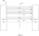
- FIG. 2 illustrates an exemplary parity check grouping according to certain aspects of the present disclosure.
- group G1 is used as an example.
- Other groups G2, ..., Gm may follow same grouping scheme.
- the plurality of data lines D1 is further divided into a plurality of sub-groups DS1, DS2, ..., DSk.
- the error check lines of group G1 are divided into a plurality of parity check lines CS1, CS2, ..., CSk, each for a corresponding one of the plurality of sub-groups DS1, DS2, ..., DSk.
- CS1, CS2, ..., CSk each for a corresponding one of the plurality of sub-groups DS1, DS2, ..., DSk.
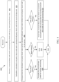
- FIG. 3 illustrates an exemplary method for sending data without additional wires for inversion signaling according to certain aspects of the present disclosure.
- the method 300 is executed by a sender (e.g., the sender 102).
- the method 300 works for a bus with one or more groups, each group being divided into a plurality of sub-groups, each one of the plurality of sub-group contains one parity check line. For illustration purpose, only one group data transmission is described. The method is equally applied to other groups if there are any.
- a new data code of the group is sent over a plurality of data lines in a portion of the bus.
- the sender calculates a parity check code (even or odd, depending on pre-selected error check scheme) for the new data code.
- the new data code is divided into a plurality of sub-groups.
- the sender calculates a parity bit for each one of the plurality of sub-group.
- the parity check code is an error check code which contains all the parity bits of the new data code. In specific implementation, the parity bits do not have to be sent through wires next to each other.
- the sender calculates a Hamming distance between the new data code of the group and a prior data code of the group.
- the prior data code of the group is the last data code sent before sending the new data code of the group over the same data lines in the same portion of the bus.
- the value of the prior data code of the group determines the current state of each data line in the bus.
- the Hamming distance for the group is checked to determine if it is greater than half of the number of bits in the new data code of the group. If it is, the sender takes action at 308.
- the sender inverts the new data code of the group and the parity check code to obtain an inverted new data code and an inverted parity check codes. By inversion, each bit of data code or parity check code is changed from logic "1" to "0" or logic "0" to "1".
- the sender sends the inverted new data code and the inverted error check code to the bus. If the Hamming distance is less than or equal to half of the number of bits in the new data code, then no inversion is needed. As a result, at 312, the sender sends the new data code and the error check code to the bus directly.
- FIG. 4 illustrates an exemplary method for receiving data without additional wires for inversion signaling according to certain aspects of the present disclosure.
- the method 400 is executed by a receiver (e.g., the receiver 104).
- a receiver e.g., the receiver 104
- only one group of data received is described below. If there is more than one group, same method applies to other groups.
- the receiver receives a data from a sender sent by the method 300 over a bus.
- the data may be divided into a plurality of groups. Each group comprises a received data code and a received parity check code.
- the received data code and the received error check code are the new data code and the error check code of the group, respectively, in the method 300 if the Hamming distance is not greater than half of the number of bits in the data. Otherwise, the received data code and the received error check code are the inverted new data code and the inverted error check code, respectively, in the method 300.
- the method 400 applies for error check being parity check.
- the even parity check is used by the sender.
- the received error check code is an even parity code.
- odd parity used by the sender same method applies by switching even parity to odd parity and odd parity to even parity.
- the receiver calculates a calculated even parity check codes and a calculated odd parity check code for the received data code. The receiver divides the received data code into a plurality of sub-groups according to the same grouping scheme in the sender.
- the receiver than calculates an even parity bit and an odd parity for each one of the plurality of sub-groups of the received data code.
- the calculated even parity check code is an error check code which contains all the even parity bits of the received data code.
- the calculated odd parity check code is an error check code which contains all the odd parity bits of the received data code.
- the receiver compares both the calculated even parity check codes and the calculated odd parity check code with the received parity check code for the group. If the calculated even parity check code matches, which is the parity used by the sender in this example, then it indicates that the received data code is non-inverted and valid. The received data code is ready to be provided for further processing, which is done at 408. However, if the calculated odd parity check code matches, then it indicates that the received data code is inverted and is valid. Therefore, the method goes to 410, where the received data code is inverted to obtain an inverted received data code and the inverted received data code is provided for further processing. If there is no match, neither even nor odd parity, then the received data code must be corrupted during transmission, an error signal should be generated at 414.
- the receiver may not have to calculate and/or match the calculated odd parity check code if it finds that even parity matches, saving power and time.
- the receiver may perform the odd parity check first and may not have to calculate and/or match the calculated even parity check code if it finds that odd parity matches.
- the methods 300 and 400 do not require inversion signal lines. This is possible as in the side of sending, the error check code is inverted together with the data code if the Hamming distance is greater than half of the number of bits in the data code. In the side of receiving, inversion and corruption of data code is checked through two comparisons: comparison between the calculated even parity check code for the received data code and the received error check code and comparison between the calculated odd parity check code for the received data code and the received error check code.
- the scheme significantly saves wiring cost. Adding wires is costly. It contributes to power dissipation and routing area. For a bus with 1024-bit data code and 64-bit grouping, area for 16 wires are saved in addition to power consumption for toggling the signals on those wires.
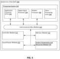
- FIG. 5 illustrates an exemplary system-on-chip (SoC) 500 implementing the data transmission without additional wires for inversion signaling according to certain aspects of the present disclosure.
- the data transmission without additional wires for inversion signaling may be implemented inside the SoC 500.
- the SoC 500 comprises a processing system 520 that includes a plurality of heterogeneous processors such as an application processor 502, a digital signal processor 504, a modem processor 506, and other processing units 508.
- the processing system 520 may include one or more cores, and each processor/core may perform operations independent of the other processors/cores.
- the processing system 520 is interconnected with one or more controller module 512, input/output (I/O) module 514, memory module 516, and system components and resources module 418 via an interconnection/bus module 510, which may include an array of reconfigurable logic gates and/or implement bus architecture (e.g., CoreConnect, advanced microcontroller bus architecture (AMBA), etc.).
- the interconnection/bus module 510 communications may be provided by advanced interconnects, such as high performance networks-on-chip (NoCs).
- the interconnection/bus module 510 may include or provide a bus mastering system configured to grant SoC components (e.g., processors, peripherals, etc.) exclusive control of the bus (e.g., to transfer data in burst mode, block transfer mode, etc.) for a set duration, number of operations, number of bytes, etc.
- SoC components e.g., processors, peripherals, etc.
- the interconnection/bus module 510 may implement an arbitration scheme to prevent multiple master components from attempting to drive the bus simultaneously.
- the interconnection/bus module 510 may comprise a plurality of buses for connecting varied components within the SoC 500.
- the memory module 516 is a computer-readable storage medium implemented in the SoC 500.
- the memory module 516 may provide non-volatile storage, such as flash memory, for one or more of the processing system 520, controller module 512, I/O module 514, and/or the system components and resources module 518.
- the memory module 516 may include a cache memory to provide temporary storage of information to enhance processing speed of the SoC 500.
- the memory module 516 may be implemented as a universal flash storage (UFS) integrated into the SoC 500, or an external UFS card.
- UFS universal flash storage
- the interconnection/bus module 510 facilitates the data transmission among the components within the SoC 500.
- the processors within the processing system 520 may transmit data between each other through the interconnect/bus module 510.
- the application processor 502 and the modem processor 506 may pass data to each other through a bus.
- the processors within the processing system 520 may transmit data to and from the memory module 516.
- the processors within the processing system 520 may transmit data to and from the input/output module 514.
- the memory module 516 may transmit data to and from the input/output module 514.
- the methods 200 and 300 may be applied to those data transmissions. With the methods 200 and 300, the interconnect/bus module 510 would be more compact and does not have to dedicate valuable power and area resource for inversion signaling.
- the methods 200 and 300 may be, for example, implemented as a firmware where executable instructions reside in the memory module 516 and executed by the one or more components in the processing system 520. Alternatively, the method 200 and 300 may be implemented as a state machine residing in one or more components of SoC 500.
- FIG. 6 illustrates an exemplary system implementing the data transmission without additional wires for inversion signaling according to certain aspects of the present disclosure.
- the system 600 may be, for example, a wireless device, an IoT device, or a computing device.
- the system 600 may comprise a plurality of components, such as an application processor SoC 602, a baseband 604, a sensor module 606, a display module 608, a memory module 610, a RF front-end 612, a power management 614, an antenna 616, and/or a battery 618, and may include more.
- the plurality of components may communicate to each other through a plurality of interconnection/buses 620, where data are transmitted.
- the plurality of interconnection/buses 620 may be different from each other, such as have different number of wire lines, different number of voltages, different error checks, or they may be the same. Some or all of transmission over the plurality interconnection/buses 620 may be implemented with the methods 300 and 400. For example, the transmission between the application processor SoC 602 with the display module 608 or between the baseband 604 and the application processor SoC 602 may use the methods 300 and 400.
- DSP digital signal processor
- ASIC application-specific integrated circuit
- FPGA field programmable gate array
- a general-purpose processor may be a microprocessor, but, in the alternative, the processor may be any conventional processor, controller, microcontroller, or state machine.
- a processor may also be implemented as a combination of computing devices, e.g., a combination of a DSP and a microprocessor, a plurality of microprocessors, one or more microprocessors in conjunction with a DSP core, or any other such configuration. Alternatively, some operations or methods may be performed by circuitry that is specific to a given function.
- the functions described may be implemented in hardware, software, firmware, or any combination thereof. If implemented in software, the functions may be stored as one or more instructions or code on a non-transitory computer-readable medium or a non-transitory processor-readable medium.
- the operations of a method or algorithm disclosed herein may be embodied in a processor-executable software module that may reside on a non-transitory computer-readable or processor-readable storage medium.
- Non-transitory computer-readable or processor-readable storage media may be any storage media that may be accessed by a computer or a processor.
- non-transitory computer-readable or processor-readable media may include RAM, ROM, EEPROM, FLASH memory, CD-ROM or other optical disk storage, magnetic disk storage or other magnetic storage devices, or any other medium that may be used to store desired program code in the form of instructions or data structures and that may be accessed by a computer.
- Disk and disc includes compact disc (CD), laser disc, optical disc, digital versatile disc (DVD), floppy disk, and Blu-ray disc where disks usually reproduce data magnetically, while discs reproduce data optically with lasers. Combinations of the above are also included within the scope of non-transitory computer-readable and processor-readable media.
- the operations of a method or algorithm may reside as one or any combination or set of codes and/or instructions on a non-transitory processor-readable medium and/or computer-readable medium, which may be incorporated into a computer program product.
Landscapes
- Engineering & Computer Science (AREA)
- Theoretical Computer Science (AREA)
- Physics & Mathematics (AREA)
- Probability & Statistics with Applications (AREA)
- General Engineering & Computer Science (AREA)
- General Physics & Mathematics (AREA)
- Computer Networks & Wireless Communication (AREA)
- Signal Processing (AREA)
- Detection And Correction Of Errors (AREA)
- Detection And Prevention Of Errors In Transmission (AREA)
Claims (15)
- Ein Verfahren (300) zum Senden von Daten über einen Bus (106), aufweisend:Berechnen (302) eines Paritätsprüfcodes für einen neuen Datencode, wobei der neue Datencode eine Anzahl von Bits in dem neuen Datencode aufweist,Berechnen (304) einer Hamming-Distanz zwischen dem neuen Datencode und einem älteren Datencode der vorausgehenden Sendung, undwenn die Hamming-Distanz größer als die Hälfte der Anzahl von Bits in dem neuen Datencode ist:Invertieren (308) des neuen Datencodes und des Paritätsprüfcodes, um einen invertierten neuen Datencode und einen invertierten Paritätsprüfcode zu erhalten, undSenden (310) des invertierten neuen Datencodes und des invertierten Paritätsprüfcodes an den Bus (106),Senden des neuen Datencodes und des Paritätsprüfcodes an den Bus (106), wenn die Hamming-Distanz nicht größer als die Hälfte der Anzahl von Bits in dem neuen Datencode ist,wobei der Bus (106) keinen Draht für eine Inversionssignalisierung enthält.
- Verfahren (300) nach Anspruch 1, wobei das Berechnen des Paritätsprüfcodes für den neuen Datencode das Berechnen eines Paritätsbits für jede aus einer Vielzahl von Subgruppen des neuen Datencodes aufweist und wobei der Paritätsprüfcode ein Fehlerprüfcode, der alle die Paritätsbits des neuen Datencodes enthält, ist.
- Verfahren (300) nach Anspruch 1, wobei der neue Datencode ein Teilsatz eines großen Datencodes von 1024 Bits ist.
- Verfahren (300) nach Anspruch 1, wobei der Paritätsprüfcode ein gerader Paritätscode ist.
- Ein Verfahren (400) zum Empfangen von Daten über einen Bus (106), aufweisend:Empfangen (402) eines empfangenen Datencodes und eines empfangenen Paritätsprüfcode eines ersten Typs von Paritätsprüfung von dem Bus (106), wobei der erste Typ von Paritätsprüfung entweder eine gerade Paritätsprüfung oder eine ungerade Paritätsprüfung ist,Berechnen (404) eines berechneten Paritätsprüfcodes eines zweiten Typs von Paritätsprüfung für den empfangenen Datencode, wobei der zweite Typ von Paritätsprüfung eine ungerade Paritätsprüfung ist, wenn der erste Typ von Paritätsprüfung eine gerade Paritätsprüfung ist, oder eine gerade Paritätsprüfung ist, wenn der erste Typ von Paritätsprüfung eine ungerade Paritätsprüfung ist, undVorsehen eines invertierten empfangenen Datencodes für eine weitere Verarbeitung, wenn der berechnete Paritätsprüfcode des zweiten Typs von Paritätsprüfung für den empfangenen Datencode dem empfangenen Paritätsprüfcode entspricht, wobei der invertierte empfangene Datencode durch das Invertieren des empfangenen Datencodes erhalten wird,wobei der Bus (106) keinen Draht für eine Inversionssignalisierung enthält.
- Verfahren (400) nach Anspruch 5, das weiterhin aufweist:Berechnen eines berechneten Paritätsprüfcodes des ersten Typs von Paritätsprüfung für den empfangenen Datencode, undVorsehen des empfangenen Datencodes für eine weitere Verarbeitung, wenn der berechnete Paritätsprüfcode des ersten Typs von Paritätsprüfung für den empfangenen Datencode dem empfangenen Paritätsprüfcode entspricht.
- Verfahren (400) nach Anspruch 6, das weiterhin das Senden eines Fehlersignals aufweist, wenn der berechnete Paritätsprüfcode des ersten Typs von Paritätsprüfung für den empfangenen Datencode nicht dem empfangenen Paritätsprüfcode entspricht und der berechnete Paritätsprüfcode des zweiten Typs von Paritätsprüfung für den empfangenen Datencode nicht dem empfangenen Paritätsprüfcode entspricht.
- Verfahren (400) nach Anspruch 5, wobei das Berechnen des berechneten Paritätsprüfcodes des zweiten Typs von Paritätsprüfung für den empfangenen Datencode das Berechnen eines Paritätsbits für jede aus einer Vielzahl von Subgruppen des empfangenen Datencodes aufweist und wobei der berechnete Paritätsprüfcode des zweiten Typs von Paritätsprüfung für den empfangenen Datencode ein Fehlerprüfcode, der alle die Paritätsbits des empfangenen Datencodes enthält, ist.
- Ein System (600), aufweisend:einen Bus (106), undeinen Sender (102), der mit dem Bus (106) gekoppelt ist und konfiguriert ist zum:Berechnen eines Paritätsprüfcodes für einen neuen Datencode, wobei der neue Datencode eine Anzahl von Bits in dem neuen Datencode enthält,Berechnen einer Hamming-Distanz zwischen dem neuen Datencode und einem älteren Datencode der vorausgehenden Sendung, undwenn die Hamming-Distanz größer als die Hälfte der Anzahl von Bits in dem neuen Datencode ist:Invertieren des neuen Datencodes und des Paritätsprüfcodes, um einen invertierten neuen Datencode und einen invertierten Paritätsprüfcode zu erhalten, undSenden des invertierten neuen Datencodes und des invertierten Paritätsprüfcodes an den Bus (106),wobei der Sender (102) weiterhin konfiguriert ist zum Senden des neuen Datencodes und des Paritätsprüfcodes an den Bus (102), wenn die Hamming-Distanz nicht größer als die Hälfte der Anzahl von Bits in dem neuen Datencode ist, undwobei der Bits (106) keinen Draht für eine Inversionssignalisierung enthält.
- System (600) nach Anspruch 9, das weiterhin einen Empfänger (104) aufweist, der mit dem Bus (106) gekoppelt ist und konfiguriert ist zum:Empfangen eines empfangenen Datencodes und eines empfangenen Paritätsprüfcodes eines ersten Typs von Paritätsprüfung von dem Bus (106), wobei der erste Typ von Paritätsprüfung entweder eine gerade Paritätsprüfung oder eine ungerade Paritätsprüfung ist,Berechnen eines berechneten Paritätsprüfcodes eines zweiten Typs von Paritätsprüfung für den empfangenen Datencode, wobei der zweite Typ von Paritätsprüfung eine ungerade Paritätsprüfung ist, wenn der erste Typ von Paritätsprüfung eine gerade Paritätsprüfung ist, oder eine gerade Paritätsprüfung ist, wenn der erste Typ von Paritätsprüfung eine ungerade Paritätsprüfung ist, undVorsehen des invertierten empfangenen Datencodes für eine weitere Verarbeitung, wenn der berechnete Paritätsprüfcode des zweiten Typs von Paritätsprüfung für den empfangenen Datencode dem empfangenen Paritätsprüfcode entspricht, wobei der invertierte empfangene Datencode durch das Invertieren des empfangenen Datencodes erhalten wird.
- System nach Anspruch 10, wobeider empfangene Datencode der neue Datencode ist, oderder empfangene Datencode der invertierte neue Datencode ist, oderder Paritätsprüfcode für den neuen Datencode der erste Typ von Paritätsprüfung ist, oderder Empfänger ein Speicher oder ein Prozessor ist, oderder Sender, der Empfänger und der Bus zu einem System-on-Chip integriert sind, oderder Sender, der Empfänger und der Bus zu einem drahtlosen Gerät integriert sind.
- Ein System (600), aufweisend:einen Bus (106), undeinen Empfänger (104), der mit dem Bus (106) gekoppelt ist und konfiguriert ist zum:Empfangen eines empfangenen Datencodes und eines empfangenen Paritätsprüfcodes eines ersten Typs von Paritätsprüfung von dem Bus (106), wobei der erste Typ von Paritätsprüfung entweder eine gerade Paritätsprüfung oder eine ungerade Paritätsprüfung ist,Berechnen eines berechneten Paritätsprüfcodes eines zweiten Typs von Paritätsprüfung für den empfangenen Datencode, wobei der zweite Typ von Paritätsprüfung eine ungerade Paritätsprüfung ist, wenn der erste Typ von Paritätsprüfung eine gerade Paritätsprüfung ist, oder eine gerade Paritätsprüfung ist, wenn der erste Typ von Paritätsprüfung eine ungerade Paritätsprüfung ist, undVorsehen eines invertierten empfangenen Datencodes für eine weitere Verarbeitung, wenn der berechnete Paritätsprüfcode des zweiten Typs von Paritätsprüfung für den empfangenen Datencode dem empfangenen Paritätsprüfcode entspricht, wobei der invertierte empfangene Datencode durch das Invertieren des empfangenen Datencodes erhalten wird,wobei der Bus (106) keinen Draht für eine Inversionssignalisierung enthält.
- System (600) nach Anspruch 12, wobei der Empfänger (104) weiterhin konfiguriert ist zum:Berechnen eines berechneten Paritätsprüfcodes des ersten Typs von Paritätsprüfung für den empfangenen Datencode, undVorsehen des empfangenen Datencodes für eine weitere Verarbeitung, wenn der berechnete Paritätsprüfcode des ersten Typs von Paritätsprüfung für den empfangenen Datencode dem empfangenen Paritätsprüfcode entspricht.
- System (600) nach Anspruch 13, wobei der Empfänger (104) weiterhin konfiguriert ist zum Vorsehen eines Fehlersignals, wenn der berechnete Paritätsprüfcode des ersten Typs von Paritätsprüfung für den empfangenen Datencode nicht dem empfangenen Paritätsprüfcode entspricht und der berechnete Paritätsprüfcode des zweiten Typs von Paritätsprüfung für den empfangenen Datencode nicht dem empfangenen Paritätsprüfcode entspricht.
- System (600) nach Anspruch 12, das weiterhin einen Sender (102) aufweist, der mit dem Bus (106) gekoppelt ist und konfiguriert ist zum Senden des empfangenen Datencodes und des empfangenen Fehlerprüfcodes an den Bus (106).
Applications Claiming Priority (2)
| Application Number | Priority Date | Filing Date | Title |
|---|---|---|---|
| US16/774,472 US11139830B2 (en) | 2020-01-28 | 2020-01-28 | Bit inversion for data transmission |
| PCT/US2021/015206 WO2021154801A1 (en) | 2020-01-28 | 2021-01-27 | Bit inversion for data transmission |
Publications (3)
| Publication Number | Publication Date |
|---|---|
| EP4097883A1 EP4097883A1 (de) | 2022-12-07 |
| EP4097883B1 true EP4097883B1 (de) | 2024-12-11 |
| EP4097883C0 EP4097883C0 (de) | 2024-12-11 |
Family
ID=74661518
Family Applications (1)
| Application Number | Title | Priority Date | Filing Date |
|---|---|---|---|
| EP21706135.7A Active EP4097883B1 (de) | 2020-01-28 | 2021-01-27 | Bitinversion für datenübertragung |
Country Status (5)
| Country | Link |
|---|---|
| US (1) | US11139830B2 (de) |
| EP (1) | EP4097883B1 (de) |
| CN (1) | CN115004587B (de) |
| TW (1) | TW202134898A (de) |
| WO (1) | WO2021154801A1 (de) |
Families Citing this family (1)
| Publication number | Priority date | Publication date | Assignee | Title |
|---|---|---|---|---|
| EP4328738A1 (de) * | 2022-08-26 | 2024-02-28 | Leuze electronic GmbH + Co. KG | Sensoranordnung |
Family Cites Families (10)
| Publication number | Priority date | Publication date | Assignee | Title |
|---|---|---|---|---|
| JP4054190B2 (ja) * | 2001-12-27 | 2008-02-27 | 松下電器産業株式会社 | データ転送システム |
| GB0419871D0 (en) | 2004-09-08 | 2004-10-13 | Koninkl Philips Electronics Nv | Fault tolerant bus |
| US8117526B2 (en) | 2007-10-29 | 2012-02-14 | Qimonda Ag | Apparatus and method for generating a transmit signal and apparatus and method for extracting an original message from a received signal |
| EP2056510B1 (de) * | 2007-10-30 | 2013-04-03 | Sony Corporation | Vorrichtung und Verfahren zur Datenverarbeitung |
| KR20090059838A (ko) * | 2007-12-07 | 2009-06-11 | 삼성전자주식회사 | 반도체 장치에서 데이터를 전송하는 방법, 장치 및 시스템 |
| US10372527B2 (en) * | 2013-07-15 | 2019-08-06 | Intel Corporation | Method of encoding data |
| US9665527B2 (en) | 2014-12-09 | 2017-05-30 | Intel Corporation | Dynamic bus inversion with programmable termination level to maintain programmable target ratio of ones and zeros in signal lines |
| FR3039922B1 (fr) * | 2015-08-06 | 2018-02-02 | Stmicroelectronics (Rousset) Sas | Procede d'ecriture dans une memoire du type eeprom et dispositif de memoire correspondant |
| US10523240B2 (en) * | 2016-06-02 | 2019-12-31 | Texas Instruments Incorporated | Methods and apparatus to determine and apply polarity-based error correction code |
| US10623200B2 (en) * | 2018-07-20 | 2020-04-14 | Nvidia Corp. | Bus-invert coding with restricted hamming distance for multi-byte interfaces |
-
2020
- 2020-01-28 US US16/774,472 patent/US11139830B2/en active Active
-
2021
- 2021-01-27 WO PCT/US2021/015206 patent/WO2021154801A1/en not_active Ceased
- 2021-01-27 CN CN202180011368.6A patent/CN115004587B/zh active Active
- 2021-01-27 EP EP21706135.7A patent/EP4097883B1/de active Active
- 2021-01-28 TW TW110103226A patent/TW202134898A/zh unknown
Also Published As
| Publication number | Publication date |
|---|---|
| CN115004587A (zh) | 2022-09-02 |
| US20210234554A1 (en) | 2021-07-29 |
| US11139830B2 (en) | 2021-10-05 |
| WO2021154801A1 (en) | 2021-08-05 |
| CN115004587B (zh) | 2023-08-08 |
| EP4097883A1 (de) | 2022-12-07 |
| TW202134898A (zh) | 2021-09-16 |
| EP4097883C0 (de) | 2024-12-11 |
Similar Documents
| Publication | Publication Date | Title |
|---|---|---|
| EP2972927B1 (de) | Datenbusumkehrkodierung, die auf der betriebsgeschwindigkeit basiert ist | |
| EP2526492B1 (de) | Datenbusumkehr mit mehreren worten | |
| US9513988B2 (en) | Method and device for increasing the data transmission capacity in a serial bus system | |
| US7965741B2 (en) | Method, apparatus, and system for idle state definition for power management | |
| US9268888B1 (en) | Latency computation circuitry | |
| US20140101356A1 (en) | Transmission device, transmission system, and control method for transmission device | |
| JP2005519518A (ja) | 高速の構成可能なトランシーバアーキテクチャ | |
| JP3683892B2 (ja) | 改良された差動形態の遷移符号化のための方法およびシステム | |
| US6553445B1 (en) | Method and apparatus for reducing noise associated with switched outputs | |
| EP4097883B1 (de) | Bitinversion für datenübertragung | |
| US11868209B2 (en) | Method and system for sequencing data checks in a packet | |
| JP2999110B2 (ja) | 無線通信方法及び無線通信装置 | |
| KR100763533B1 (ko) | 버스 인버팅 코드 생성 장치 및 이를 이용한 버스 인버팅코드 생성 방법 | |
| US7320094B2 (en) | Retraining derived clock receivers | |
| CN119583503A (zh) | 信号处理方法、装置及系统 | |
| US8201071B2 (en) | Information transmission and reception | |
| US11726944B2 (en) | Transaction layer circuit of PCIe and operation method thereof | |
| WO2021017726A1 (zh) | 改善传输速率的方法、处理器、网络设备和网络系统 | |
| US10846085B2 (en) | Multi-lane data processing circuit and system | |
| CN112104537B (zh) | 一种通信控制器 | |
| US20240372643A1 (en) | Data transmission method and data transmission apparatus | |
| Chaki et al. | Design and Simulation of a 3 port Bidirectional Router with Suspend-Based Flow Control | |
| JP2874983B2 (ja) | 通信装置 | |
| CN117376123A (zh) | 模式协商方法、装置、设备、系统及计算机可读存储介质 | |
| CN120729484A (zh) | 信号处理方法、终端设备及计算机可读存储介质 |
Legal Events
| Date | Code | Title | Description |
|---|---|---|---|
| STAA | Information on the status of an ep patent application or granted ep patent |
Free format text: STATUS: UNKNOWN |
|
| STAA | Information on the status of an ep patent application or granted ep patent |
Free format text: STATUS: THE INTERNATIONAL PUBLICATION HAS BEEN MADE |
|
| PUAI | Public reference made under article 153(3) epc to a published international application that has entered the european phase |
Free format text: ORIGINAL CODE: 0009012 |
|
| STAA | Information on the status of an ep patent application or granted ep patent |
Free format text: STATUS: REQUEST FOR EXAMINATION WAS MADE |
|
| 17P | Request for examination filed |
Effective date: 20220615 |
|
| AK | Designated contracting states |
Kind code of ref document: A1 Designated state(s): AL AT BE BG CH CY CZ DE DK EE ES FI FR GB GR HR HU IE IS IT LI LT LU LV MC MK MT NL NO PL PT RO RS SE SI SK SM TR |
|
| DAV | Request for validation of the european patent (deleted) | ||
| DAX | Request for extension of the european patent (deleted) | ||
| GRAP | Despatch of communication of intention to grant a patent |
Free format text: ORIGINAL CODE: EPIDOSNIGR1 |
|
| STAA | Information on the status of an ep patent application or granted ep patent |
Free format text: STATUS: GRANT OF PATENT IS INTENDED |
|
| INTG | Intention to grant announced |
Effective date: 20240709 |
|
| GRAS | Grant fee paid |
Free format text: ORIGINAL CODE: EPIDOSNIGR3 |
|
| GRAA | (expected) grant |
Free format text: ORIGINAL CODE: 0009210 |
|
| STAA | Information on the status of an ep patent application or granted ep patent |
Free format text: STATUS: THE PATENT HAS BEEN GRANTED |
|
| AK | Designated contracting states |
Kind code of ref document: B1 Designated state(s): AL AT BE BG CH CY CZ DE DK EE ES FI FR GB GR HR HU IE IS IT LI LT LU LV MC MK MT NL NO PL PT RO RS SE SI SK SM TR |
|
| REG | Reference to a national code |
Ref country code: GB Ref legal event code: FG4D |
|
| REG | Reference to a national code |
Ref country code: CH Ref legal event code: EP |
|
| REG | Reference to a national code |
Ref country code: DE Ref legal event code: R096 Ref document number: 602021023234 Country of ref document: DE |
|
| REG | Reference to a national code |
Ref country code: IE Ref legal event code: FG4D |
|
| U01 | Request for unitary effect filed |
Effective date: 20241223 |
|
| U07 | Unitary effect registered |
Designated state(s): AT BE BG DE DK EE FI FR IT LT LU LV MT NL PT RO SE SI Effective date: 20250113 |
|
| PG25 | Lapsed in a contracting state [announced via postgrant information from national office to epo] |
Ref country code: HR Free format text: LAPSE BECAUSE OF FAILURE TO SUBMIT A TRANSLATION OF THE DESCRIPTION OR TO PAY THE FEE WITHIN THE PRESCRIBED TIME-LIMIT Effective date: 20241211 |
|
| PG25 | Lapsed in a contracting state [announced via postgrant information from national office to epo] |
Ref country code: ES Free format text: LAPSE BECAUSE OF FAILURE TO SUBMIT A TRANSLATION OF THE DESCRIPTION OR TO PAY THE FEE WITHIN THE PRESCRIBED TIME-LIMIT Effective date: 20241211 |
|
| PGFP | Annual fee paid to national office [announced via postgrant information from national office to epo] |
Ref country code: IE Payment date: 20250326 Year of fee payment: 5 |
|
| PG25 | Lapsed in a contracting state [announced via postgrant information from national office to epo] |
Ref country code: NO Free format text: LAPSE BECAUSE OF FAILURE TO SUBMIT A TRANSLATION OF THE DESCRIPTION OR TO PAY THE FEE WITHIN THE PRESCRIBED TIME-LIMIT Effective date: 20250311 |
|
| PG25 | Lapsed in a contracting state [announced via postgrant information from national office to epo] |
Ref country code: GR Free format text: LAPSE BECAUSE OF FAILURE TO SUBMIT A TRANSLATION OF THE DESCRIPTION OR TO PAY THE FEE WITHIN THE PRESCRIBED TIME-LIMIT Effective date: 20250312 |
|
| PGFP | Annual fee paid to national office [announced via postgrant information from national office to epo] |
Ref country code: GB Payment date: 20250313 Year of fee payment: 5 |
|
| PG25 | Lapsed in a contracting state [announced via postgrant information from national office to epo] |
Ref country code: RS Free format text: LAPSE BECAUSE OF FAILURE TO SUBMIT A TRANSLATION OF THE DESCRIPTION OR TO PAY THE FEE WITHIN THE PRESCRIBED TIME-LIMIT Effective date: 20250311 |
|
| U20 | Renewal fee for the european patent with unitary effect paid |
Year of fee payment: 5 Effective date: 20250326 |
|
| PG25 | Lapsed in a contracting state [announced via postgrant information from national office to epo] |
Ref country code: SM Free format text: LAPSE BECAUSE OF FAILURE TO SUBMIT A TRANSLATION OF THE DESCRIPTION OR TO PAY THE FEE WITHIN THE PRESCRIBED TIME-LIMIT Effective date: 20241211 |
|
| PG25 | Lapsed in a contracting state [announced via postgrant information from national office to epo] |
Ref country code: PL Free format text: LAPSE BECAUSE OF FAILURE TO SUBMIT A TRANSLATION OF THE DESCRIPTION OR TO PAY THE FEE WITHIN THE PRESCRIBED TIME-LIMIT Effective date: 20241211 |
|
| PG25 | Lapsed in a contracting state [announced via postgrant information from national office to epo] |
Ref country code: IS Free format text: LAPSE BECAUSE OF FAILURE TO SUBMIT A TRANSLATION OF THE DESCRIPTION OR TO PAY THE FEE WITHIN THE PRESCRIBED TIME-LIMIT Effective date: 20250411 |
|
| PG25 | Lapsed in a contracting state [announced via postgrant information from national office to epo] |
Ref country code: SK Free format text: LAPSE BECAUSE OF FAILURE TO SUBMIT A TRANSLATION OF THE DESCRIPTION OR TO PAY THE FEE WITHIN THE PRESCRIBED TIME-LIMIT Effective date: 20241211 |
|
| PG25 | Lapsed in a contracting state [announced via postgrant information from national office to epo] |
Ref country code: CZ Free format text: LAPSE BECAUSE OF FAILURE TO SUBMIT A TRANSLATION OF THE DESCRIPTION OR TO PAY THE FEE WITHIN THE PRESCRIBED TIME-LIMIT Effective date: 20241211 |
|
| REG | Reference to a national code |
Ref country code: CH Ref legal event code: PL |
|
| PG25 | Lapsed in a contracting state [announced via postgrant information from national office to epo] |
Ref country code: MC Free format text: LAPSE BECAUSE OF FAILURE TO SUBMIT A TRANSLATION OF THE DESCRIPTION OR TO PAY THE FEE WITHIN THE PRESCRIBED TIME-LIMIT Effective date: 20241211 |
|
| PLBE | No opposition filed within time limit |
Free format text: ORIGINAL CODE: 0009261 |
|
| STAA | Information on the status of an ep patent application or granted ep patent |
Free format text: STATUS: NO OPPOSITION FILED WITHIN TIME LIMIT |
|
| PG25 | Lapsed in a contracting state [announced via postgrant information from national office to epo] |
Ref country code: CH Free format text: LAPSE BECAUSE OF NON-PAYMENT OF DUE FEES Effective date: 20250131 |
|
| 26N | No opposition filed |
Effective date: 20250912 |