EP4095920A1 - Display panel and display apparatus - Google Patents
Display panel and display apparatus Download PDFInfo
- Publication number
- EP4095920A1 EP4095920A1 EP20886208.6A EP20886208A EP4095920A1 EP 4095920 A1 EP4095920 A1 EP 4095920A1 EP 20886208 A EP20886208 A EP 20886208A EP 4095920 A1 EP4095920 A1 EP 4095920A1
- Authority
- EP
- European Patent Office
- Prior art keywords
- electric connecting
- layer
- insulating layer
- base substrate
- bonding region
- Prior art date
- Legal status (The legal status is an assumption and is not a legal conclusion. Google has not performed a legal analysis and makes no representation as to the accuracy of the status listed.)
- Granted
Links
Images


Classifications
-
- H—ELECTRICITY
- H10—SEMICONDUCTOR DEVICES; ELECTRIC SOLID-STATE DEVICES NOT OTHERWISE PROVIDED FOR
- H10K—ORGANIC ELECTRIC SOLID-STATE DEVICES
- H10K59/00—Integrated devices, or assemblies of multiple devices, comprising at least one organic light-emitting element covered by group H10K50/00
- H10K59/10—OLED displays
- H10K59/12—Active-matrix OLED [AMOLED] displays
- H10K59/131—Interconnections, e.g. wiring lines or terminals
-
- G—PHYSICS
- G02—OPTICS
- G02F—OPTICAL DEVICES OR ARRANGEMENTS FOR THE CONTROL OF LIGHT BY MODIFICATION OF THE OPTICAL PROPERTIES OF THE MEDIA OF THE ELEMENTS INVOLVED THEREIN; NON-LINEAR OPTICS; FREQUENCY-CHANGING OF LIGHT; OPTICAL LOGIC ELEMENTS; OPTICAL ANALOGUE/DIGITAL CONVERTERS
- G02F1/00—Devices or arrangements for the control of the intensity, colour, phase, polarisation or direction of light arriving from an independent light source, e.g. switching, gating or modulating; Non-linear optics
- G02F1/01—Devices or arrangements for the control of the intensity, colour, phase, polarisation or direction of light arriving from an independent light source, e.g. switching, gating or modulating; Non-linear optics for the control of the intensity, phase, polarisation or colour
- G02F1/13—Devices or arrangements for the control of the intensity, colour, phase, polarisation or direction of light arriving from an independent light source, e.g. switching, gating or modulating; Non-linear optics for the control of the intensity, phase, polarisation or colour based on liquid crystals, e.g. single liquid crystal display cells
- G02F1/133—Constructional arrangements; Operation of liquid crystal cells; Circuit arrangements
- G02F1/1333—Constructional arrangements; Manufacturing methods
- G02F1/1345—Conductors connecting electrodes to cell terminals
-
- G—PHYSICS
- G06—COMPUTING OR CALCULATING; COUNTING
- G06F—ELECTRIC DIGITAL DATA PROCESSING
- G06F3/00—Input arrangements for transferring data to be processed into a form capable of being handled by the computer; Output arrangements for transferring data from processing unit to output unit, e.g. interface arrangements
- G06F3/01—Input arrangements or combined input and output arrangements for interaction between user and computer
- G06F3/03—Arrangements for converting the position or the displacement of a member into a coded form
- G06F3/041—Digitisers, e.g. for touch screens or touch pads, characterised by the transducing means
- G06F3/0412—Digitisers structurally integrated in a display
-
- G—PHYSICS
- G06—COMPUTING OR CALCULATING; COUNTING
- G06F—ELECTRIC DIGITAL DATA PROCESSING
- G06F3/00—Input arrangements for transferring data to be processed into a form capable of being handled by the computer; Output arrangements for transferring data from processing unit to output unit, e.g. interface arrangements
- G06F3/01—Input arrangements or combined input and output arrangements for interaction between user and computer
- G06F3/03—Arrangements for converting the position or the displacement of a member into a coded form
- G06F3/041—Digitisers, e.g. for touch screens or touch pads, characterised by the transducing means
- G06F3/044—Digitisers, e.g. for touch screens or touch pads, characterised by the transducing means by capacitive means
- G06F3/0446—Digitisers, e.g. for touch screens or touch pads, characterised by the transducing means by capacitive means using a grid-like structure of electrodes in at least two directions, e.g. using row and column electrodes
-
- G—PHYSICS
- G09—EDUCATION; CRYPTOGRAPHY; DISPLAY; ADVERTISING; SEALS
- G09G—ARRANGEMENTS OR CIRCUITS FOR CONTROL OF INDICATING DEVICES USING STATIC MEANS TO PRESENT VARIABLE INFORMATION
- G09G3/00—Control arrangements or circuits, of interest only in connection with visual indicators other than cathode-ray tubes
-
- H—ELECTRICITY
- H10—SEMICONDUCTOR DEVICES; ELECTRIC SOLID-STATE DEVICES NOT OTHERWISE PROVIDED FOR
- H10K—ORGANIC ELECTRIC SOLID-STATE DEVICES
- H10K59/00—Integrated devices, or assemblies of multiple devices, comprising at least one organic light-emitting element covered by group H10K50/00
- H10K59/10—OLED displays
- H10K59/12—Active-matrix OLED [AMOLED] displays
- H10K59/122—Pixel-defining structures or layers, e.g. banks
-
- H—ELECTRICITY
- H10—SEMICONDUCTOR DEVICES; ELECTRIC SOLID-STATE DEVICES NOT OTHERWISE PROVIDED FOR
- H10K—ORGANIC ELECTRIC SOLID-STATE DEVICES
- H10K59/00—Integrated devices, or assemblies of multiple devices, comprising at least one organic light-emitting element covered by group H10K50/00
- H10K59/40—OLEDs integrated with touch screens
-
- G—PHYSICS
- G06—COMPUTING OR CALCULATING; COUNTING
- G06F—ELECTRIC DIGITAL DATA PROCESSING
- G06F2203/00—Indexing scheme relating to G06F3/00 - G06F3/048
- G06F2203/041—Indexing scheme relating to G06F3/041 - G06F3/045
- G06F2203/04103—Manufacturing, i.e. details related to manufacturing processes specially suited for touch sensitive devices
-
- H—ELECTRICITY
- H10—SEMICONDUCTOR DEVICES; ELECTRIC SOLID-STATE DEVICES NOT OTHERWISE PROVIDED FOR
- H10K—ORGANIC ELECTRIC SOLID-STATE DEVICES
- H10K2102/00—Constructional details relating to the organic devices covered by this subclass
- H10K2102/301—Details of OLEDs
- H10K2102/311—Flexible OLED
Definitions
- the present disclosure relates to the field of display, in particular to a display panel and a display device.
- the present disclosure discloses a display panel and a display device, and aims to improve the laminated structure of a bonding region and avoid the occurrence of defects caused by corrosion of connection terminals.
- the embodiment of the present disclosure provides a display panel, including:
- the first bonding region is a chip bonding region
- the second bonding region is a flexible circuit board bonding region.
- the display panel further includes first lead wires disposed between the first connection terminals and the second connection terminals, where the first lead wires are disposed on the same layer as the second electric connecting structure; and the second electric connecting structures of the first connection terminals are connected with the second electric connecting structures of the second connection terminals through the first lead wires.
- the display panel further includes: a first layer of source and drain electrodes located in the display region, where the first layer of source and drain electrodes are disposed between the base substrate and the first insulating layer, and the first electric connecting structures and the first layer of source and drain electrodes are prepared on the same layer; and a second layer of source and drain electrodes located in the display region, wherein the second layer of source and drain electrodes are disposed between the first insulating layer and the second insulating layer, and the second electric connecting structures and the second layer of source and drain electrodes are prepared on the same layer; and the first insulating layer is a passivation layer, and the second insulating layer is a flat layer.
- the second insulating layer includes a first thinned portion overlapping the first bonding region and a second thinned portion overlapping the second bonding region, a thickness of the first thinned portion of the second insulating layer is smaller than a thickness of a portion surrounding the first thinned portion, and a thickness of the second thinned portion of the second insulating layer is smaller than a thickness of a portion surrounding the second thinned portion.
- the each connection terminal further includes a third electric connecting structure disposed on the second opening of the second insulating layer, and the third electric connecting structure and the second electric connecting structure of the each connection terminal are connected through the second opening; and the display panel further includes touch electrodes located in the display region, where the touch electrodes are disposed on one side, facing away from the base substrate, of the second insulating layer, and the third electric connecting structures and the touch electrodes are prepared on the same layer.
- orthographic projections of the first electric connecting structure and the second electric connecting structure of each second connection terminal on the base substrate overlap, and the orthographic projections of the first openings on the base substrate overlap the orthographic projections of the second openings on the base substrate.
- an orthographic projection of the first electric connecting structure and an orthographic projection of the second electric connecting structure of the each connection terminal on the base substrate are disposed within an orthographic projection of the third electric connecting structure of the each connection terminal on the base substrate.
- the display panel further includes a pixel definition layer disposed between the second insulating layer and a layer where the touch electrodes are located, where the pixel definition layer is located within the display region.
- the display panel further includes an organic over coating disposed on one side, facing away from the base substrate, of a layer where the touch electrodes are located, where the organic over coating is provided with a third opening exposing the first bonding region and a fourth opening exposing the second bonding region; an orthographic projection of the first thinned portion on the base substrate is located in an orthographic projection of the third opening on the base substrate; and an orthographic projection of the fourth opening on the base substrate is located in an orthographic projection of the second thinned portion on the base substrate.
- the display panel further includes a third insulating layer disposed between the first insulating layer and a layer where the second layer of source and drain electrodes are located, where the third insulating layer is a flat layer disposed in the display region.
- the first electric connecting structures and the second electric connecting structures are a titanium/aluminum/titanium laminated structure.
- a display device including the display panel of any one of the embodiments of the present disclosure.
- FIG. 1 to 5 specifically, sectional diagrams of a display panel of Fig. 1 in directions of A1-A2, B1-B2, and C1-C2 correspond to Figs. 2 , 3 , and 5 , respectively.
- the display panel includes:
- connection terminals of the bonding region 11 include the layer of first electric connecting structures 21 and the layer of second electric connecting structures 22, the first insulating layer 31 is disposed between the layer where the first electric connecting structures 21 are located and the layer where the second electric connecting structures 22 are located, and the second insulating layer 32 is disposed on the side, facing away from the base substrate 1, of the layer where the second electric connecting structures 22 are located.
- the first insulating layer 31 is provided with the first openings 311 to electrically connect the two layers of structures (the first electric connecting structures 21 and the second electric connecting structures 22) of the second connection terminals 2002, and a size of the first openings 31 is smaller than that of the first electric connecting structures 21, that is, the first insulating layer 31 wraps side surfaces of the first electric connecting structures 21 of the second connection terminals 2002, and therefore, it can be ensured that the side surfaces of the first electric connecting structures 21 of the second connection terminals 2002 cannot be corroded in a subsequent preparation process of the display panel; similarly, the second insulating layer 32 is provided with the second openings 41 such that upper portions of the second electric connecting structures 22 of the second connection terminals 2002 are exposed for bonding connection of the connection terminals, or exposed for connection between a subsequently formed third layer of structures (for example, third electric connecting structures 23 mentioned later) of the connection terminals and the two layers of structures below, and the size of the second openings 41 is smaller than an opening size of the
- an orthographic projection of the first insulating layer 31 does not overlap orthographic projections of the first connection terminals 2001, that is, the first insulating layer 31 does not wrap side surfaces of the first electric connecting structures 21 of the first connection terminals 2001, and the second electric connecting structures 22 of the first connection terminals 2001 directly cover the first electric connecting structures 21;
- the second insulating layer 32 is provided with the second openings 41 such that upper portions of the second electric connecting structures 22 of the first connection terminals 2001 are exposed for bonding connection of the connection terminals, or connection between a subsequently formed third layer of structures of the connection terminals and the two layers of structures below, and the size of the second openings 41 is smaller than an opening size of the second electric connecting structures 22 of the first connection terminals 2001, that is, the second insulating layer 32 wraps side surfaces of the first connection terminals 2001, and therefore, it can be ensured that side surfaces of the second electric connecting structures 22 cannot be corroded in the subsequent preparation process.
- the first connection terminals 2001 in the first bonding region 111 are not prone to being corroded, either, and occurrence of defects due to corrosion of the connection terminals can be avoided.
- the orthographic projection of the first insulating layer 31 does not overlap the orthographic projections of the first connection terminals 2001, that is, the first insulating layer 31 does not wrap edges of the first electric connecting structures 21 of the first connection terminals 2001, and the second electric connecting structures 22 of the first connection terminals 2001 directly cover the first electric connecting structures 21, a height difference of the first connection terminals 2001 is small, thereby being more suitable for bonding highly requiring a height difference of connection terminals, for example, bonding of integrated circuit chips.
- the display panel of the present disclosure includes the first bonding region 111 and the second bonding region 112, and the side surfaces of the connection terminals in the first bonding region 111 and the second bonding region 112 are all wrapped and protected, so that the problem of corrosion of the connection terminals is not easy to occur, defects (such as poor bonding contact or poor short circuit) caused by corrosion of the side surfaces of the connection terminals (such as lateral corrosion of the connection terminals in a subsequent anode wet etching process) can be avoided, and the yield of the display panel is improved.
- the first connection terminals 2001 in the first bonding region 111 and the second connection terminals 2002 in the second bonding region 112 are different in both film design and height difference, so as to be suitable for bonding connection with different height difference requirements, and the yield of the bonding connection is improved.
- the first bonding region 111 is a chip bonding region, e.g. a chip on polyimide (COP) region
- the second bonding region 112 is a flexible circuit board bonding region, e.g., a flexible printed circuit on polyimide (FOP) region.
- COP chip on polyimide
- FOP flexible printed circuit on polyimide
- a pitch of connection terminals (e.g. pads) of the FOP region is large and requirements on a height difference of the pads are not high, so that the second bonding region 112 is suitably configured as the FOP region.
- a pitch of pads of the COP region is small and requirements on a height difference of the pads are high, so that the first bonding region 111 is suitably configured as the COP region.
- the display panel further includes first lead wires 221 disposed between the first connection terminals 2001 and the second connection terminals 2002.
- the first lead wires 221 are disposed on the same layer as the second electric connecting structures 22, where 'being disposed on the same layer' means that it is possible to form in the same layer in a manufacturing process, e.g. forming by a patterning process with the same material layer.
- the second electric connecting structures 22 of the first connection terminals 2001 and the second electric connecting structures 22 of the second connection terminals 2002 are connected through the first lead wires 221.
- the display panel further includes a first layer of source and drain electrodes 51 and a second layer of source and drain electrodes 52 (lapping electrode layers) disposed in the display region.
- the first layer of source and drain electrodes 51 are disposed between the base substrate 1 and the first insulating layer 31, and the second layer of source and drain electrodes 52 are disposed between the first insulating layer 31 and the second insulating layer 32.
- the first electric connecting structures 21 are prepared on the same layer as the first layer of source and drain electrodes 51
- the second electric connecting structures 22 are prepared on the same layer as the second layer of source and drain electrodes 52.
- the first insulating layer 31 is a passivation layer (PVX) and is mainly configured to insulate the first layer of source and drain electrodes 51 from the second layer of source and drain electrodes 52, and also configured to protect the first layer of source and drain electrodes 51; and the second insulating layer 32 is a flat layer that functions as a flat layer and protects underlying metal electrodes and traces.
- PVX passivation layer
- the display panel provided by an embodiment of the present disclosure includes a plurality of pixel structures located in the display region 12, where the pixel structures include pixel driving circuits, the pixel driving circuits may include thin film transistors 501, storage capacitors 502 and the like.
- the pixel driving circuits may include active layers 53, a first gate insulating layer 34, gate electrodes 54, first capacitance electrodes 55, a second gate insulating layer 35, second capacitance electrodes 56, an interlayer insulating layer 36, the first layer of source and drain electrodes 51 (including source electrodes 511 and drain electrodes 512), the first insulating layer (passivation layer) 31, the second layer of source and drain electrodes 52, and the second insulating layer (flat layer) 32 which are sequentially disposed on a buffer layer 33.
- the gate electrodes 54 can be disposed on the same layer as second lead wires 541, where the second lead wires 541 are disposed between the display region and the first bonding region; the first layer of source and drain electrodes 51 can be disposed on the same layer as the first electric connecting structures 21 in the bonding region; the second layer of source and drain electrodes 52 can be disposed on the same layer as the second electric connecting structures 22 in the bonding region and the first lead wires 221; the second gate insulating layer 35 extends into the bonding region so as to protect the second lead wires 541 against corrosion; the first insulating layer 31 is configured as the passivation layer, extends into the first bonding region 111 and wraps the side surfaces of the first electric connecting structures 21 so as to protect the side surfaces of the first electric connecting structures 21 against corrosion; and the second insulating layer 32 is configured as the flat layer and extends into the first bonding region 111 and the second bonding region 112 to protect the first lead wires 221 and
- An embodiment of the present disclosure is a double-layer source and drain (SD) electrode driving panel, where connection terminals are provided with two layers of structures (first electric connecting structures 21 and second electric connecting structures 22) which are prepared on the same layer as double-layer source and drain electrodes (SD), so that a thickness of the connection terminals can be increased, a resistance is reduced, that is, a resistance drop (IR Drop) is reduced, the attenuation of signals is reduced, and the display uniformity is improved.
- a back plane of the double-layer source and drain electrodes (SD) requires the addition of two to three mask processes relative to a back plane of a conventional single-layer source and drain (SD) electrode, and a film stack structure is relatively complicated.
- the first electric connecting structures 21 and the second electric connecting structures 22 are of the same material as the source and drain electrodes, namely, a titanium/aluminum/titanium (Ti/Al/Ti) composite material, which includes two titanium material layers 202 and an aluminum material layer 201 disposed between the two titanium material layers 202, thereby forming a titanium/aluminum/titanium (Ti/Al/Ti) laminated structure.
- Ti/Al/Ti titanium/aluminum/titanium
- Fig. 4A when a side surface of an electric connecting structure is exposed, the aluminum material layer 201 in the middle of the electric connecting structure is easily corroded sideways, resulting in suspension of the titanium material layer 202 of a top layer.
- Fig. 4B an edge of the titanium material layer 202 of a top layer is easily peeled off in a later high-voltage process, resulting in metal particles 203, and if these peeled metal particles 203 remain at signal lines, a short will occur, resulting in poor display.
- Figs. 4A when a side surface of an electric connecting structure is exposed, the aluminum material layer 201 in the middle of the electric connecting structure is easily corroded sideways, resulting in suspension of the titanium material layer 202 of a top layer.
- Fig. 4B an edge of the titanium material layer 202 of a top layer is easily peeled off in a later high-voltage process, resulting in metal particles 203, and if these peeled metal particles 203 remain at signal lines,
- the side surfaces of the first electric connecting structures 21 are wrapped and protected by the first insulating layer 31, and the side surfaces of the second electric connecting structures 22 are wrapped and protected by the second insulating layer 32, thereby effectively avoiding the occurrence of defects caused by corrosion; and for the first connection terminals 2001 in the first bonding region, the side surfaces of the first electric connecting structures 21 are wrapped and protected by the second electric connecting structures 22, and the side surfaces of the second electric connecting structures 22 are wrapped and protected by the second insulating layer 32, thereby also effectively avoiding the occurrence of defects caused by corrosion.
- the display panel of an embodiment of the present disclosure may further include a third insulating layer 37 disposed between the first insulating layer 31 and the second layer of source and drain electrodes 52, where the third insulating layer 37 is a flat layer and is disposed within the display region 12.
- the third insulating layer 6 is an organic flat layer mainly functioning as a flat layer and protecting the first layer of source and drain electrodes 51.
- the passivation layer (the first insulating layer 31) and the organic flat layer (the third insulating layer 37) are disposed between the first layer of source and drain electrodes 51 and the second layer of source and drain electrodes 52; and a thickness of the passivation layer (the first insulating layer 31) is smaller than that of the organic flat layer (the third insulating layer 37).
- using the passivation layer (the first insulating layer 31) to protect the first electric connecting structures 21 of the second connection terminals 2002 instead of the organic flat layer (the third insulating layer 37), may avoid influences on bonding of the second connection terminals 2002 caused by a large edge thickness of the second connection terminals 2002.
- the third insulating layer (the organic flat layer) 37 is only disposed in the display region 11 and does not cover the bonding region 11, thereby further avoiding influences on bonding caused by an excessively large insulating layer thickness of the bonding region 11, and greatly relieving the problem of module bonding caused by film stack complexity of the double SD.
- the passivation layer (the first insulating layer 31) covers the second bonding region and wraps the edges of the second connection terminals 2002, and at the same time, the passivation layer (the first insulating layer 31) does not overlap the first bonding region, and neither covers the first bonding region nor wraps the edges of the first connection terminals 2001, so that the requirements of the COP region and the FOP region for the film thickness and the height difference of the connection terminals are matched as much as possible and the bonding yield is improved.
- the base substrate 1 may further include a bending region 13 disposed between the first bonding region 111 and the display region 12, the second lead wires 541 span the bending region 13, and two ends of the second lead wires 541 are electrically connected to the pixel driving circuits of the display region 12 and the first connection terminals 2001 of the first bonding region 111, respectively; and after bonding, the base substrate 1 may be bent along the bending region 13 to bend the bonding region 11 to a back side of the display panel.
- the first insulating layer (the passivation layer) 31 is not disposed in the bending region 13, that is, the first insulating layer (the passivation layer) 31 does not cover the bending region 13, so that the bending stress and the bending radius are reduced, the bending operation of the display panel is easier, and undesirable problems such as film or wiring breakage do not occur in the bending region 13.
- the second insulating layer 32 includes a first thinned portion 321 overlapping the first bonding region 111 and a second thinned portion 322 overlapping the second bonding region 112.
- a thickness of the first thinned portion 321 of the second insulating layer 32 is smaller than a thickness of a portion surrounding the first thinned portion 321, and a thickness of the second thinned portion 322 of the second insulating layer 32 is smaller than a thickness of a portion surrounding the second thinned portion 322, that is, portions, within the first bonding region 111 and the second bonding region 112, of the second insulating layer 32 are thinned.
- the second insulating layer 32 is an organic layer functioning as flattening and protecting, and generally has a large thickness, thinning the second insulating layer 32 in the bonding region 11 can effectively reduce the influence of the thickness of the second insulating layer 32 on bonding, thereby not only protecting the side surfaces of the connection terminals, but also greatly relieving the problem of module bonding caused by the film stack complexity of the double SD.
- a Halftone process may be employed such that the thickness of the second insulating layer in the first bonding region and the second bonding region is less than those of surrounding portions, thereby thinning the second insulating layer in the first bonding region and the second bonding region.
- connection terminals further include third electric connecting structures 23 disposed on the second openings 321 of the second insulating layer 32, and the third electric connecting structure 23 and the second electric connecting structure 22 of each connection terminal are connected through the corresponding second opening 321.
- the display panel further includes touch electrodes 7 disposed in the display region 12, where the touch electrodes 7 are disposed on one side, facing away from the base substrate 1, of the second insulating layer 32, and the third electric connecting structures 23 are prepared on the same layer as the touch electrodes 7.
- a flexible multi layer on cell touch (FMLOC) technology is adopted, and a touch sensor is formed through a film deposition process.
- the first electric connecting structures 21, the second electric connecting structures 22 and the third electric connecting structures 23 are simultaneously integrated in the connection terminals of the embodiments of the present disclosure, which can be used for transmission connection of display signals and transmission connection of touch signals.
- the connection terminals of the embodiments of the present disclosure which can be used for transmission connection of display signals and transmission connection of touch signals.
- connection terminals of the embodiments of the present disclosure a part of the connection terminals are used as connection terminals for the display signals, and the second lead wires 541 connected to those connection terminals are electrically connected to the first layer of source and drain electrodes 51 in the display region 12 without being electrically connected to the touch electrodes 7; and further, the other part of the connection terminals are used as connection terminals for the touch signals, the second lead wires 541 connected to those connection terminals are electrically connected to the touch electrodes 7 in the display region 12 without being electrically connected to the double-layer source and drain electrodes (51 and 52).
- connection between the second lead wires 541 and the electrodes of the different layers may be achieved through via holes in the interlayer insulating layer.
- connection terminals in the second bonding region, the orthographic projections of the first electric connecting structures 21 and the second electric connecting structures 22 of the second connection terminals 2002 on the base substrate 1 overlap, and the orthographic projections of the first openings 31 on the base substrate 1 and the orthographic projections of the second openings 41 on the base substrate 1 overlap.
- the connection terminals can be conveniently miniaturized, and the contact yield of each layer of the connection terminals is guaranteed.
- the orthographic projections of the first electric connecting structures 21 and the second electric connecting structures 22 on the base substrate 1 are disposed within orthographic projections of the third electric connecting structures 23 on the base substrate 1, that is, the third electric connecting structures 23 completely cover the first electric connecting structures 21 and the second electric connecting structures 22, so that a bonding contact area of the connection terminals 2 is increased, and the bonding yield is increased.
- the display panel further includes a pixel definition layer (PDL) 8 disposed between the second insulating layer 32 and a layer where the touch electrodes 7 are disposed.
- the pixel definition layer 8 (organic layer) is only within the display region 12 and does not cover the bonding region 11, so that the insulating layer thickness of the bonding region 11 is further prevented from being too large to influence bonding, and the problem of module bonding caused by film stack complexity of the double SD can be greatly relieved.
- light-emitting elements 4 are further disposed in the display region of the base substrate 1, and the light-emitting elements 4 are formed on the pixel driving circuits, that is, the light-emitting elements 4 are disposed on one side, away from the base substrate 1, of the second insulating layer (the flat layer) 32.
- Each light-emitting element 4 includes a first electrode 41, a light-emitting layer 42, and a second electrode 43.
- the first electrodes 41 of the light-emitting elements 4 are electrically connected to the second layer of source and drain electrodes (the lapping electrode layers) 52 through via holes in the second insulating layer (the flat layer) 32.
- the pixel definition layer 8 is disposed on the first electrodes 41, the pixel definition layer 8 includes a plurality of openings for defining a plurality of pixel cells, each opening exposes one first electrode 41, and the light-emitting layers 42 are disposed in the plurality of openings of the pixel definition layer 8.
- the second electrodes 43 may be disposed in a part or the whole of the display region, so that the second electrodes 43 may be integrally formed in the manufacturing process.
- each encapsulation layer 91 includes a first organic layer 911, an inorganic layer 912, and a second organic layer 913.
- the encapsulation layers 91 do not cover the bonding region, i.e., not overlapping the bonding region.
- the touch electrodes 7 are disposed on one side, facing away from the base substrate 1, of the encapsulation layers 91.
- the display panel may further include an organic over coating (OC) 9 disposed on one side, facing away from the base substrate 1, of the layer where the touch electrodes 7 are disposed.
- the organic over coating 92 is provided with a third opening 921 exposing the first bonding region 111 and a fourth opening 922 exposing the second bonding region 112.
- the organic over coating is provided with the openings for avoiding the first bonding region and the second bonding region, that is, the organic over coating does not cover the first bonding region and the second bonding region, so that the thickness of the insulating layer in the bonding region is prevented from being too large to influence bonding.
- the organic over coating only avoids the bonding region, but covers other regions, thereby having a good protection effect on underlying metal wiring.
- an orthographic projection of the first thinned portion 321 of the second insulating layer 32 on the base substrate 1 is disposed within an orthographic projection of the third opening 921 of the organic over coating 92 on the base substrate 1
- an orthographic projection of the fourth opening 922 of the organic over coating 92 on the base substrate 1 is disposed within an orthographic projection of the second thinned portion 322 of the second insulating layer 32 on the base substrate 1.
- an opening boundary (a boundary of the fourth opening 922) of the organic over coating 92 surrounds an edge of a thinned region (an edge of the second thinned portion 322) of the second insulating layer 32
- an edge of a thinned region (an edge of the first thinned portion 321) of the second insulating layer 32 surrounds an opening boundary (a boundary of the third opening 921) of the organic over coating 92.
- the actual product is not limited to the above case, and in an actual display panel product, it is also possible that in the FOP region, the opening boundary (the boundary of the third opening 921) of the organic over coating 92 surrounds the edge of the thinned region (the edge of the first thinned portion 321) of the second insulating layer 32, and in the COP region, the edge of the thinned region (the edge of the second thinned portion 322) of the second insulating layer 32 surrounds the opening boundary (the boundary of the fourth opening 922) of the organic over coating 92.
- the display panel in the embodiments of the present disclosure may be a flexible active-matrix organic light-emitting diode (AMOLED) display panel, where the base substrate is a flexible base and includes double-layer polyimide (PI) and an inorganic layer disposed in the middle of the double-layer PI; and alternatively, the display panel of the embodiments of the present disclosure may be a rigid panel, where the base substrate is glass.
- AMOLED active-matrix organic light-emitting diode
- an embodiment of the present disclosure provides a display device including the display panel of any one of the embodiments of the present disclosure as described the above.
- the display device provided by the embodiments of the present disclosure has the same beneficial effects as the display panel of the embodiments of the present disclosure, and is not described in detail herein.
Landscapes
- Engineering & Computer Science (AREA)
- Physics & Mathematics (AREA)
- Theoretical Computer Science (AREA)
- General Engineering & Computer Science (AREA)
- General Physics & Mathematics (AREA)
- Human Computer Interaction (AREA)
- Microelectronics & Electronic Packaging (AREA)
- Nonlinear Science (AREA)
- Crystallography & Structural Chemistry (AREA)
- Chemical & Material Sciences (AREA)
- Optics & Photonics (AREA)
- Computer Hardware Design (AREA)
- Mathematical Physics (AREA)
- Electroluminescent Light Sources (AREA)
- Devices For Indicating Variable Information By Combining Individual Elements (AREA)
Abstract
Description
- The present disclosure relates to the field of display, in particular to a display panel and a display device.
- The use of a double-layer source and drain (SD) electrode process on a backplane will increase the laminated structure of a display device, especially in a bonding region, the film structure design has a very obvious impact on the bonding effect. Attendant process problems are what we must consider to deal with, for example, in a flexible printed circuit (FPC) on polyimide (PI) (FOP) region of a flexible substrate, it is common to encounter a corrosion problem of a metal layer of a connection terminal (e.g. pad), that is, in a bonding region of an FPC, due to the bare metal cross-section of the Pad, the Pad is easily corroded sideways, which will influence the bonding effect and yield. In severe cases, the precipitation of metal ions caused by corrosion will cause short circuits in a display region, causing more serious display problems.
- The present disclosure discloses a display panel and a display device, and aims to improve the laminated structure of a bonding region and avoid the occurrence of defects caused by corrosion of connection terminals.
- The embodiment of the present disclosure provides a display panel, including:
- a base substrate provided with a display region and a bonding region, where the bonding region is located on one side of the display region, and is divided into a first bonding region and a second bonding region, and the first bonding region is located between the display region and the second bonding region;
- a plurality of connection terminals located in the bonding regions, where each connection terminal includes a first electric connecting structure and a second electric connecting structure which are sequentially stacked on the base substrate, and the plurality of connection terminals include a plurality of first connection terminals located in the first bonding region and a plurality of second connection terminals located in the second bonding region;
- a first insulating layer disposed between a layer where the first electric connecting structure is located and a layer where the second electric connecting structure is located, where an orthographic projection of the first insulating layer on the base substrate does not overlap an orthographic projection of the first connection terminal on the base substrate, the first insulating layer overlaps the second bonding region and is provided with a plurality of first openings corresponding to the plurality of second connection terminals, an orthographic projection of each first opening on the base substrate is disposed within an orthographic projection of the first electric connecting structure of the corresponding second connection terminal on the base substrate, and the first electric connecting structure and the second electric connecting structure of each second connection terminal are connected through the corresponding first opening; and
- a second insulating layer disposed on one side, facing away from the base substrate, of the layer where the second electric connecting structure is located, where the second insulating layer overlaps the bonding region and is provided with a plurality of second openings corresponding to the plurality of connection terminals, and an orthographic projection of each second opening on the base substrate is disposed within an orthographic projection of the second electric connecting structure of the corresponding connection terminal on the base substrate.
- Optionally, the first bonding region is a chip bonding region, and the second bonding region is a flexible circuit board bonding region.
- Optionally, the display panel further includes first lead wires disposed between the first connection terminals and the second connection terminals, where the first lead wires are disposed on the same layer as the second electric connecting structure; and the second electric connecting structures of the first connection terminals are connected with the second electric connecting structures of the second connection terminals through the first lead wires.
- Optionally, the display panel further includes: a first layer of source and drain electrodes located in the display region, where the first layer of source and drain electrodes are disposed between the base substrate and the first insulating layer, and the first electric connecting structures and the first layer of source and drain electrodes are prepared on the same layer; and a second layer of source and drain electrodes located in the display region, wherein the second layer of source and drain electrodes are disposed between the first insulating layer and the second insulating layer, and the second electric connecting structures and the second layer of source and drain electrodes are prepared on the same layer; and the first insulating layer is a passivation layer, and the second insulating layer is a flat layer.
- Optionally, the second insulating layer includes a first thinned portion overlapping the first bonding region and a second thinned portion overlapping the second bonding region, a thickness of the first thinned portion of the second insulating layer is smaller than a thickness of a portion surrounding the first thinned portion, and a thickness of the second thinned portion of the second insulating layer is smaller than a thickness of a portion surrounding the second thinned portion.
- Optionally, the each connection terminal further includes a third electric connecting structure disposed on the second opening of the second insulating layer, and the third electric connecting structure and the second electric connecting structure of the each connection terminal are connected through the second opening; and the display panel further includes touch electrodes located in the display region, where the touch electrodes are disposed on one side, facing away from the base substrate, of the second insulating layer, and the third electric connecting structures and the touch electrodes are prepared on the same layer.
- Optionally, in the second bonding region, orthographic projections of the first electric connecting structure and the second electric connecting structure of each second connection terminal on the base substrate overlap, and the orthographic projections of the first openings on the base substrate overlap the orthographic projections of the second openings on the base substrate.
- Optionally, an orthographic projection of the first electric connecting structure and an orthographic projection of the second electric connecting structure of the each connection terminal on the base substrate are disposed within an orthographic projection of the third electric connecting structure of the each connection terminal on the base substrate.
- Optionally, the display panel further includes a pixel definition layer disposed between the second insulating layer and a layer where the touch electrodes are located, where the pixel definition layer is located within the display region.
- Optionally, the display panel further includes an organic over coating disposed on one side, facing away from the base substrate, of a layer where the touch electrodes are located, where the organic over coating is provided with a third opening exposing the first bonding region and a fourth opening exposing the second bonding region; an orthographic projection of the first thinned portion on the base substrate is located in an orthographic projection of the third opening on the base substrate; and an orthographic projection of the fourth opening on the base substrate is located in an orthographic projection of the second thinned portion on the base substrate.
- Optionally, the display panel further includes a third insulating layer disposed between the first insulating layer and a layer where the second layer of source and drain electrodes are located, where the third insulating layer is a flat layer disposed in the display region.
- Optionally, the first electric connecting structures and the second electric connecting structures are a titanium/aluminum/titanium laminated structure.
- A display device is provided, including the display panel of any one of the embodiments of the present disclosure.
-
-
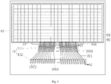
Fig. 1 is a schematic structural diagram of a display panel according to an embodiment of the present disclosure. -
Fig. 2 is a sectional schematic structural diagram of the display panel ofFig. 1 in a direction of A1-A2. -
Fig. 3 is a sectional schematic structural diagram of the display panel ofFig. 1 in a direction of B1-B2. -
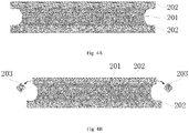
Fig. 4A is a sectional schematic structural diagram illustrating a case where a part of the structure of connection terminals of the display panel is corroded, according to an embodiment of the present disclosure. -
Fig. 4B is a sectional schematic structural diagram illustrating a case where a part of the structure of the connection terminals of the display panel is corroded to produce a bad condition, according to an embodiment of the present disclosure. -
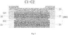
Fig. 5 is a sectional schematic structural diagram of the display panel ofFig. 1 in a direction of C1-C2. - The technical solutions of the embodiments of the present disclosure are described clearly and thoroughly with reference to the accompanying drawings of the embodiments of the present disclosure hereinafter. It is to be understood that the described embodiments are some, but not all, embodiments of the present disclosure. Based on the described embodiments of the present disclosure, all other embodiments attainable by those of ordinary skill in the art without involving any inventive effort are within the scope of the present disclosure.
- Referring to
Figs. 1 to 5 , specifically, sectional diagrams of a display panel ofFig. 1 in directions of A1-A2, B1-B2, and C1-C2 correspond toFigs. 2 ,3 , and5 , respectively. - As shown in
Figs. 1 and2 , embodiments of the present disclosure provide a display panel. The display panel includes: - a
base substrate 1 provided with adisplay region 12 and a bonding region 11 disposed on one side of thedisplay region 12, where the bonding region 11 is divided into a first bonding region 111 and asecond bonding region 112, and the first bonding region 111 is disposed between thedisplay region 12 and thesecond bonding region 112; - a plurality of connection terminals located in the bonding region 11, where each connection terminal includes a first
electric connecting structure 21 and a secondelectric connecting structure 22 which are sequentially stacked on thebase substrate 1, and the plurality of connection terminals include a plurality offirst connection terminals 2001 disposed in the first bonding region 111 and a plurality ofsecond connection terminals 2002 disposed in thesecond bonding region 112; - a
first insulating layer 31 disposed between a layer where the firstelectric connecting structures 21 are located and a layer where the secondelectric connecting structures 22 are located, where an orthographic projection of the firstinsulating layer 31 on thebase substrate 1 does not overlap orthographic projections of thefirst connection terminals 2001 on thebase substrate 1, the firstinsulating layer 31 overlaps thesecond bonding region 112 and is provided with a plurality offirst openings 31 corresponding to the plurality ofsecond connection terminals 2002, an orthographic projection of eachfirst opening 311 on thebase substrate 1 is disposed within an orthographic projection of the firstelectric connecting structure 21 of the correspondingsecond connection terminal 2002 on thebase substrate 1, and the firstelectric connecting structure 21 and the secondelectric connecting structure 22 of eachsecond connection terminal 2002 are connected through the correspondingfirst opening 311; and - a second
insulating layer 32 disposed on one side, facing away from thebase substrate 1, of the layer where the secondelectric connecting structures 22 are located, where thesecond insulating layer 32 overlaps the bonding region 11 and is provided with a plurality ofsecond openings 321 corresponding to the plurality of connection terminals (the plurality offirst connection terminals 2001 and the plurality of second connection terminals 2002), and an orthographic projection of each second opening 321 on thebase substrate 1 is disposed within an orthographic projection of the secondelectric connecting structure 22 of the corresponding connection terminal on thebase substrate 1. - In the above-mentioned display panel, the connection terminals of the bonding region 11 include the layer of first
electric connecting structures 21 and the layer of secondelectric connecting structures 22, thefirst insulating layer 31 is disposed between the layer where the firstelectric connecting structures 21 are located and the layer where the secondelectric connecting structures 22 are located, and the secondinsulating layer 32 is disposed on the side, facing away from thebase substrate 1, of the layer where the secondelectric connecting structures 22 are located. - Specifically, in the
second bonding region 112, thefirst insulating layer 31 is provided with thefirst openings 311 to electrically connect the two layers of structures (the firstelectric connecting structures 21 and the second electric connecting structures 22) of thesecond connection terminals 2002, and a size of thefirst openings 31 is smaller than that of the firstelectric connecting structures 21, that is, the firstinsulating layer 31 wraps side surfaces of the firstelectric connecting structures 21 of thesecond connection terminals 2002, and therefore, it can be ensured that the side surfaces of the firstelectric connecting structures 21 of thesecond connection terminals 2002 cannot be corroded in a subsequent preparation process of the display panel; similarly, the secondinsulating layer 32 is provided with thesecond openings 41 such that upper portions of the secondelectric connecting structures 22 of thesecond connection terminals 2002 are exposed for bonding connection of the connection terminals, or exposed for connection between a subsequently formed third layer of structures (for example, thirdelectric connecting structures 23 mentioned later) of the connection terminals and the two layers of structures below, and the size of thesecond openings 41 is smaller than an opening size of the secondelectric connecting structures 22, that is, the secondinsulating layer 32 wraps side surfaces of the secondelectric connecting structures 22 of thesecond connection terminals 2002, and therefore, it can be ensured that the side surfaces of the secondelectric connecting structures 22 cannot be corroded in the subsequent preparation process. Therefore, thesecond connection terminals 2002 in thesecond bonding region 112 are not prone to being corroded, and occurrence of defects due to corrosion of the connection terminals can be avoided. - In the first bonding region 111, an orthographic projection of the first
insulating layer 31 does not overlap orthographic projections of thefirst connection terminals 2001, that is, thefirst insulating layer 31 does not wrap side surfaces of the firstelectric connecting structures 21 of thefirst connection terminals 2001, and the secondelectric connecting structures 22 of thefirst connection terminals 2001 directly cover the firstelectric connecting structures 21; thesecond insulating layer 32 is provided with thesecond openings 41 such that upper portions of the secondelectric connecting structures 22 of thefirst connection terminals 2001 are exposed for bonding connection of the connection terminals, or connection between a subsequently formed third layer of structures of the connection terminals and the two layers of structures below, and the size of thesecond openings 41 is smaller than an opening size of the secondelectric connecting structures 22 of thefirst connection terminals 2001, that is, the secondinsulating layer 32 wraps side surfaces of thefirst connection terminals 2001, and therefore, it can be ensured that side surfaces of the secondelectric connecting structures 22 cannot be corroded in the subsequent preparation process. Therefore, thefirst connection terminals 2001 in the first bonding region 111 are not prone to being corroded, either, and occurrence of defects due to corrosion of the connection terminals can be avoided. Meanwhile, since the orthographic projection of the first insulatinglayer 31 does not overlap the orthographic projections of thefirst connection terminals 2001, that is, thefirst insulating layer 31 does not wrap edges of the firstelectric connecting structures 21 of thefirst connection terminals 2001, and the secondelectric connecting structures 22 of thefirst connection terminals 2001 directly cover the firstelectric connecting structures 21, a height difference of thefirst connection terminals 2001 is small, thereby being more suitable for bonding highly requiring a height difference of connection terminals, for example, bonding of integrated circuit chips. - In summary, the display panel of the present disclosure includes the first bonding region 111 and the
second bonding region 112, and the side surfaces of the connection terminals in the first bonding region 111 and thesecond bonding region 112 are all wrapped and protected, so that the problem of corrosion of the connection terminals is not easy to occur, defects (such as poor bonding contact or poor short circuit) caused by corrosion of the side surfaces of the connection terminals (such as lateral corrosion of the connection terminals in a subsequent anode wet etching process) can be avoided, and the yield of the display panel is improved. Moreover, according to different bonding process requirements, thefirst connection terminals 2001 in the first bonding region 111 and thesecond connection terminals 2002 in thesecond bonding region 112 are different in both film design and height difference, so as to be suitable for bonding connection with different height difference requirements, and the yield of the bonding connection is improved. - In a specific embodiment, as shown in
Fig. 1 , the first bonding region 111 is a chip bonding region, e.g. a chip on polyimide (COP) region, and thesecond bonding region 112 is a flexible circuit board bonding region, e.g., a flexible printed circuit on polyimide (FOP) region. - Specifically, a pitch of connection terminals (e.g. pads) of the FOP region is large and requirements on a height difference of the pads are not high, so that the
second bonding region 112 is suitably configured as the FOP region. A pitch of pads of the COP region is small and requirements on a height difference of the pads are high, so that the first bonding region 111 is suitably configured as the COP region. - In a specific embodiment, as shown in
Figs. 1 and2 , the display panel further includesfirst lead wires 221 disposed between thefirst connection terminals 2001 and thesecond connection terminals 2002. Thefirst lead wires 221 are disposed on the same layer as the secondelectric connecting structures 22, where 'being disposed on the same layer' means that it is possible to form in the same layer in a manufacturing process, e.g. forming by a patterning process with the same material layer. - The second
electric connecting structures 22 of thefirst connection terminals 2001 and the secondelectric connecting structures 22 of thesecond connection terminals 2002 are connected through thefirst lead wires 221. - In a specific embodiment, as shown in
Fig. 3 , the display panel further includes a first layer of source anddrain electrodes 51 and a second layer of source and drain electrodes 52 (lapping electrode layers) disposed in the display region. Specifically, the first layer of source anddrain electrodes 51 are disposed between thebase substrate 1 and the firstinsulating layer 31, and the second layer of source anddrain electrodes 52 are disposed between the firstinsulating layer 31 and the secondinsulating layer 32. As shown inFigs. 2 and3 , the firstelectric connecting structures 21 are prepared on the same layer as the first layer of source anddrain electrodes 51, and the secondelectric connecting structures 22 are prepared on the same layer as the second layer of source anddrain electrodes 52. - Specifically, the
first insulating layer 31 is a passivation layer (PVX) and is mainly configured to insulate the first layer of source anddrain electrodes 51 from the second layer of source anddrain electrodes 52, and also configured to protect the first layer of source anddrain electrodes 51; and the secondinsulating layer 32 is a flat layer that functions as a flat layer and protects underlying metal electrodes and traces. - As shown in
Figs. 1 and3 , the display panel provided by an embodiment of the present disclosure includes a plurality of pixel structures located in thedisplay region 12, where the pixel structures include pixel driving circuits, the pixel driving circuits may includethin film transistors 501,storage capacitors 502 and the like. Specifically, the pixel driving circuits may includeactive layers 53, a firstgate insulating layer 34,gate electrodes 54, first capacitance electrodes 55, a secondgate insulating layer 35,second capacitance electrodes 56, aninterlayer insulating layer 36, the first layer of source and drain electrodes 51 (includingsource electrodes 511 and drain electrodes 512), the first insulating layer (passivation layer) 31, the second layer of source anddrain electrodes 52, and the second insulating layer (flat layer) 32 which are sequentially disposed on abuffer layer 33. - Specifically, as shown in
Figs. 2 and3 , thegate electrodes 54 can be disposed on the same layer as secondlead wires 541, where the secondlead wires 541 are disposed between the display region and the first bonding region; the first layer of source and drainelectrodes 51 can be disposed on the same layer as the firstelectric connecting structures 21 in the bonding region; the second layer of source and drainelectrodes 52 can be disposed on the same layer as the secondelectric connecting structures 22 in the bonding region and the firstlead wires 221; the secondgate insulating layer 35 extends into the bonding region so as to protect the secondlead wires 541 against corrosion; the first insulatinglayer 31 is configured as the passivation layer, extends into the first bonding region 111 and wraps the side surfaces of the firstelectric connecting structures 21 so as to protect the side surfaces of the firstelectric connecting structures 21 against corrosion; and the second insulatinglayer 32 is configured as the flat layer and extends into the first bonding region 111 and thesecond bonding region 112 to protect the firstlead wires 221 and the side surfaces of the secondelectric connecting structures 22 of the connection terminals against corrosion. - An embodiment of the present disclosure is a double-layer source and drain (SD) electrode driving panel, where connection terminals are provided with two layers of structures (first electric connecting
structures 21 and second electric connecting structures 22) which are prepared on the same layer as double-layer source and drain electrodes (SD), so that a thickness of the connection terminals can be increased, a resistance is reduced, that is, a resistance drop (IR Drop) is reduced, the attenuation of signals is reduced, and the display uniformity is improved. Specifically, a back plane of the double-layer source and drain electrodes (SD) requires the addition of two to three mask processes relative to a back plane of a conventional single-layer source and drain (SD) electrode, and a film stack structure is relatively complicated. - Illustratively, as shown in
Figs. 4A and 4B , the firstelectric connecting structures 21 and the secondelectric connecting structures 22 are of the same material as the source and drain electrodes, namely, a titanium/aluminum/titanium (Ti/Al/Ti) composite material, which includes two titanium material layers 202 and analuminum material layer 201 disposed between the two titanium material layers 202, thereby forming a titanium/aluminum/titanium (Ti/Al/Ti) laminated structure. - Specifically, as shown in
Fig. 4A , when a side surface of an electric connecting structure is exposed, thealuminum material layer 201 in the middle of the electric connecting structure is easily corroded sideways, resulting in suspension of thetitanium material layer 202 of a top layer. As shown inFig. 4B , an edge of thetitanium material layer 202 of a top layer is easily peeled off in a later high-voltage process, resulting inmetal particles 203, and if these peeledmetal particles 203 remain at signal lines, a short will occur, resulting in poor display. As shown inFigs. 2 and5 , according to the display panel of the present disclosure, for thesecond connection terminals 2002 in the second bonding region, the side surfaces of the firstelectric connecting structures 21 are wrapped and protected by the first insulatinglayer 31, and the side surfaces of the secondelectric connecting structures 22 are wrapped and protected by the second insulatinglayer 32, thereby effectively avoiding the occurrence of defects caused by corrosion; and for thefirst connection terminals 2001 in the first bonding region, the side surfaces of the firstelectric connecting structures 21 are wrapped and protected by the secondelectric connecting structures 22, and the side surfaces of the secondelectric connecting structures 22 are wrapped and protected by the second insulatinglayer 32, thereby also effectively avoiding the occurrence of defects caused by corrosion. - In a specific embodiment, as shown in
Fig. 3 , the display panel of an embodiment of the present disclosure may further include a third insulatinglayer 37 disposed between the first insulatinglayer 31 and the second layer of source and drainelectrodes 52, where the third insulatinglayer 37 is a flat layer and is disposed within thedisplay region 12. - Specifically, the third insulating layer 6 is an organic flat layer mainly functioning as a flat layer and protecting the first layer of source and drain
electrodes 51. - As shown in
Figs. 2 and3 , the passivation layer (the first insulating layer 31) and the organic flat layer (the third insulating layer 37) are disposed between the first layer of source and drainelectrodes 51 and the second layer of source and drainelectrodes 52; and a thickness of the passivation layer (the first insulating layer 31) is smaller than that of the organic flat layer (the third insulating layer 37). In the present disclosure, using the passivation layer (the first insulating layer 31) to protect the firstelectric connecting structures 21 of thesecond connection terminals 2002, instead of the organic flat layer (the third insulating layer 37), may avoid influences on bonding of thesecond connection terminals 2002 caused by a large edge thickness of thesecond connection terminals 2002. In addition, the third insulating layer (the organic flat layer) 37 is only disposed in the display region 11 and does not cover the bonding region 11, thereby further avoiding influences on bonding caused by an excessively large insulating layer thickness of the bonding region 11, and greatly relieving the problem of module bonding caused by film stack complexity of the double SD. - Specifically, as shown in
Fig. 2 , the passivation layer (the first insulating layer 31) covers the second bonding region and wraps the edges of thesecond connection terminals 2002, and at the same time, the passivation layer (the first insulating layer 31) does not overlap the first bonding region, and neither covers the first bonding region nor wraps the edges of thefirst connection terminals 2001, so that the requirements of the COP region and the FOP region for the film thickness and the height difference of the connection terminals are matched as much as possible and the bonding yield is improved. - In a specific embodiment, as shown in
Fig. 1 , in the display panel of the present disclosure, thebase substrate 1 may further include a bendingregion 13 disposed between the first bonding region 111 and thedisplay region 12, the secondlead wires 541 span the bendingregion 13, and two ends of the secondlead wires 541 are electrically connected to the pixel driving circuits of thedisplay region 12 and thefirst connection terminals 2001 of the first bonding region 111, respectively; and after bonding, thebase substrate 1 may be bent along the bendingregion 13 to bend the bonding region 11 to a back side of the display panel. - Specifically, the first insulating layer (the passivation layer) 31 is not disposed in the bending
region 13, that is, the first insulating layer (the passivation layer) 31 does not cover the bendingregion 13, so that the bending stress and the bending radius are reduced, the bending operation of the display panel is easier, and undesirable problems such as film or wiring breakage do not occur in the bendingregion 13. - In a specific embodiment, as shown in
Figs. 1 and2 , the second insulatinglayer 32 includes a first thinnedportion 321 overlapping the first bonding region 111 and a second thinnedportion 322 overlapping thesecond bonding region 112. As shown inFig. 2 , a thickness of the first thinnedportion 321 of the second insulatinglayer 32 is smaller than a thickness of a portion surrounding the first thinnedportion 321, and a thickness of the second thinnedportion 322 of the second insulatinglayer 32 is smaller than a thickness of a portion surrounding the second thinnedportion 322, that is, portions, within the first bonding region 111 and thesecond bonding region 112, of the second insulatinglayer 32 are thinned. The second insulatinglayer 32 is an organic layer functioning as flattening and protecting, and generally has a large thickness, thinning the second insulatinglayer 32 in the bonding region 11 can effectively reduce the influence of the thickness of the second insulatinglayer 32 on bonding, thereby not only protecting the side surfaces of the connection terminals, but also greatly relieving the problem of module bonding caused by the film stack complexity of the double SD. - Specifically, a Halftone process may be employed such that the thickness of the second insulating layer in the first bonding region and the second bonding region is less than those of surrounding portions, thereby thinning the second insulating layer in the first bonding region and the second bonding region.
- In a specific embodiment, as shown in
Figs. 2 and5 , the connection terminals further include third electric connectingstructures 23 disposed on thesecond openings 321 of the second insulatinglayer 32, and the thirdelectric connecting structure 23 and the secondelectric connecting structure 22 of each connection terminal are connected through the correspondingsecond opening 321. - Specifically, as shown in
Figs. 1 to 3 , the display panel further includes touch electrodes 7 disposed in thedisplay region 12, where the touch electrodes 7 are disposed on one side, facing away from thebase substrate 1, of the second insulatinglayer 32, and the third electric connectingstructures 23 are prepared on the same layer as the touch electrodes 7. - According to the display panel disclosed by the embodiments of the present disclosure, a flexible multi layer on cell touch (FMLOC) technology is adopted, and a touch sensor is formed through a film deposition process.
- Specifically, as shown in
Fig. 2 , the firstelectric connecting structures 21, the secondelectric connecting structures 22 and the third electric connectingstructures 23 are simultaneously integrated in the connection terminals of the embodiments of the present disclosure, which can be used for transmission connection of display signals and transmission connection of touch signals. For example, as shown inFigs. 1 to 3 , among all the connection terminals of the embodiments of the present disclosure, a part of the connection terminals are used as connection terminals for the display signals, and the secondlead wires 541 connected to those connection terminals are electrically connected to the first layer of source and drainelectrodes 51 in thedisplay region 12 without being electrically connected to the touch electrodes 7; and further, the other part of the connection terminals are used as connection terminals for the touch signals, the secondlead wires 541 connected to those connection terminals are electrically connected to the touch electrodes 7 in thedisplay region 12 without being electrically connected to the double-layer source and drain electrodes (51 and 52). Illustratively, connection between the secondlead wires 541 and the electrodes of the different layers may be achieved through via holes in the interlayer insulating layer. - In a specific embodiment, as shown in
Figs. 2 and5 , in the second bonding region, the orthographic projections of the firstelectric connecting structures 21 and the secondelectric connecting structures 22 of thesecond connection terminals 2002 on thebase substrate 1 overlap, and the orthographic projections of thefirst openings 31 on thebase substrate 1 and the orthographic projections of thesecond openings 41 on thebase substrate 1 overlap. According to the arrangement, the connection terminals can be conveniently miniaturized, and the contact yield of each layer of the connection terminals is guaranteed. - Illustratively, as shown in
Figs. 2 and5 , the orthographic projections of the firstelectric connecting structures 21 and the secondelectric connecting structures 22 on thebase substrate 1 are disposed within orthographic projections of the third electric connectingstructures 23 on thebase substrate 1, that is, the third electric connectingstructures 23 completely cover the firstelectric connecting structures 21 and the secondelectric connecting structures 22, so that a bonding contact area of the connection terminals 2 is increased, and the bonding yield is increased. - In a specific embodiment, as shown in
Figs. 1 and3 , the display panel further includes a pixel definition layer (PDL) 8 disposed between the second insulatinglayer 32 and a layer where the touch electrodes 7 are disposed. The pixel definition layer 8 (organic layer) is only within thedisplay region 12 and does not cover the bonding region 11, so that the insulating layer thickness of the bonding region 11 is further prevented from being too large to influence bonding, and the problem of module bonding caused by film stack complexity of the double SD can be greatly relieved. - Specifically, as shown in
Fig. 3 , light-emittingelements 4 are further disposed in the display region of thebase substrate 1, and the light-emittingelements 4 are formed on the pixel driving circuits, that is, the light-emittingelements 4 are disposed on one side, away from thebase substrate 1, of the second insulating layer (the flat layer) 32. Each light-emittingelement 4 includes afirst electrode 41, a light-emittinglayer 42, and asecond electrode 43. Thefirst electrodes 41 of the light-emittingelements 4 are electrically connected to the second layer of source and drain electrodes (the lapping electrode layers) 52 through via holes in the second insulating layer (the flat layer) 32. Thepixel definition layer 8 is disposed on thefirst electrodes 41, thepixel definition layer 8 includes a plurality of openings for defining a plurality of pixel cells, each opening exposes onefirst electrode 41, and the light-emittinglayers 42 are disposed in the plurality of openings of thepixel definition layer 8. Thesecond electrodes 43 may be disposed in a part or the whole of the display region, so that thesecond electrodes 43 may be integrally formed in the manufacturing process. - Further, as shown in
Fig. 3 , the light-emittingelements 4 are further provided with encapsulation layers 91. Eachencapsulation layer 91 includes a firstorganic layer 911, aninorganic layer 912, and a secondorganic layer 913. The encapsulation layers 91 do not cover the bonding region, i.e., not overlapping the bonding region. Specifically, the touch electrodes 7 are disposed on one side, facing away from thebase substrate 1, of the encapsulation layers 91. - Further, as shown in
Figs. 2 and3 , the display panel may further include an organic over coating (OC) 9 disposed on one side, facing away from thebase substrate 1, of the layer where the touch electrodes 7 are disposed. As shown inFigs. 1 and2 , the organic overcoating 92 is provided with athird opening 921 exposing the first bonding region 111 and afourth opening 922 exposing thesecond bonding region 112. - The organic over coating is provided with the openings for avoiding the first bonding region and the second bonding region, that is, the organic over coating does not cover the first bonding region and the second bonding region, so that the thickness of the insulating layer in the bonding region is prevented from being too large to influence bonding. In addition, the organic over coating only avoids the bonding region, but covers other regions, thereby having a good protection effect on underlying metal wiring.
- Specifically, as shown in
Fig. 2 , an orthographic projection of the first thinnedportion 321 of the second insulatinglayer 32 on thebase substrate 1 is disposed within an orthographic projection of thethird opening 921 of the organic overcoating 92 on thebase substrate 1, and an orthographic projection of thefourth opening 922 of the organic overcoating 92 on thebase substrate 1 is disposed within an orthographic projection of the second thinnedportion 322 of the second insulatinglayer 32 on thebase substrate 1. That is, in the first bonding region (COP region), an opening boundary (a boundary of the fourth opening 922) of the organic overcoating 92 surrounds an edge of a thinned region (an edge of the second thinned portion 322) of the second insulatinglayer 32, and in the second bonding region (FOP region), an edge of a thinned region (an edge of the first thinned portion 321) of the second insulatinglayer 32 surrounds an opening boundary (a boundary of the third opening 921) of the organic overcoating 92. - Certainly, the actual product is not limited to the above case, and in an actual display panel product, it is also possible that in the FOP region, the opening boundary (the boundary of the third opening 921) of the organic over
coating 92 surrounds the edge of the thinned region (the edge of the first thinned portion 321) of the second insulatinglayer 32, and in the COP region, the edge of the thinned region (the edge of the second thinned portion 322) of the second insulatinglayer 32 surrounds the opening boundary (the boundary of the fourth opening 922) of the organic overcoating 92. - Specifically, the display panel in the embodiments of the present disclosure may be a flexible active-matrix organic light-emitting diode (AMOLED) display panel, where the base substrate is a flexible base and includes double-layer polyimide (PI) and an inorganic layer disposed in the middle of the double-layer PI; and alternatively, the display panel of the embodiments of the present disclosure may be a rigid panel, where the base substrate is glass.
- In addition, an embodiment of the present disclosure provides a display device including the display panel of any one of the embodiments of the present disclosure as described the above.
- The display device provided by the embodiments of the present disclosure has the same beneficial effects as the display panel of the embodiments of the present disclosure, and is not described in detail herein.
- It will be apparent to those skilled in the art that various modifications and variations can be made in the disclosed embodiments without departing from the spirit or scope of the disclosure. Thus, it is intended that the present disclosure covers the modifications and variations of this disclosure provided they come within the scope of the appended claims and their equivalents.
Claims (13)
- A display panel, comprising:a base substrate, comprising a display region and a bonding region, wherein the bonding region is located on a side of the display region and is divided into a first bonding region and a second bonding region, wherein the first bonding region is located between the display region and the second bonding region;a plurality of connection terminals, located in the bonding region, wherein each connection terminal comprises a first electric connecting structure and a second electric connecting structure which are sequentially stacked on the base substrate, and the plurality of connection terminals comprise a plurality of first connection terminals located in the first bonding region and a plurality of second connection terminals located in the second bonding region;a first insulating layer disposed between a layer where the first electric connecting structure is located and a layer where the second electric connecting structure is located, wherein an orthographic projection of the first insulating layer on the base substrate does not overlap an orthographic projection of the first connection terminal on the base substrate, the first insulating layer overlaps the second bonding region and is provided with a plurality of first openings corresponding to the plurality of second connection terminals, an orthographic projection of each first opening on the base substrate is disposed within an orthographic projection of the first electric connecting structure of the corresponding second connection terminal on the base substrate, and the first electric connecting structure and the second electric connecting structure of each second connection terminal are connected through the corresponding first opening; anda second insulating layer disposed on a side, facing away from the base substrate, of the layer where the second electric connecting structure is located, wherein the second insulating layer overlaps the bonding region and is provided with a plurality of second openings corresponding to the plurality of connection terminals, and an orthographic projection of each second opening on the base substrate is disposed within an orthographic projection of the second electric connecting structure of the corresponding connection terminal on the base substrate.
- The display panel according to claim 1, wherein the first bonding region is a chip bonding region and the second bonding region is a flexible circuit board bonding region.
- The display panel according to claim 1, further comprising first lead wires disposed between the first connection terminals and the second connection terminals, wherein the first lead wires are disposed on the same layer as the second electric connecting structure; and
the second electric connecting structures of the first connection terminals are connected with the second electric connecting structures of the second connection terminals through the first lead wires. - The display panel according to any one of claims 1 to 3, further comprising:a first layer of source and drain electrodes located in the display region and disposed between the base substrate and the first insulating layer, wherein the first electric connecting structures and the first layer of source and drain electrodes are prepared on the same layer; anda second layer of source and drain electrodes located in the display region and disposed between the first insulating layer and the second insulating layer, wherein the second electric connecting structures and the second layer of source and drain electrodes are prepared on the same layer;wherein the first insulating layer is a passivation layer, and the second insulating layer is a flat layer.
- The display panel according to claim 4, wherein the second insulating layer comprises a first thinned portion overlapping the first bonding region and a second thinned portion overlapping the second bonding region, wherein a thickness of the first thinned portion of the second insulating layer is smaller than a thickness of a portion surrounding the first thinned portion, and a thickness of the second thinned portion of the second insulating layer is smaller than a thickness of a portion surrounding the second thinned portion.
- The display panel according to claim 5, wherein the each connection terminal further comprises a third electric connecting structure disposed on the second opening of the second insulating layer, wherein the third electric connecting structure and the second electric connecting structure of the each connection terminal are connected through the second opening; and
the display panel further comprises touch electrodes located in the display region and disposed on a side, facing away from the base substrate, of the second insulating layer, and the third electric connecting structures and the touch electrodes are prepared on the same layer. - The display panel according to claim 6, wherein in the second bonding region, orthographic projections of the first electric connecting structure and the second electric connecting structure of each second connection terminal on the base substrate overlap, and the orthographic projections of the first openings on the base substrate overlap the orthographic projections of the second openings on the base substrate.
- The display panel according to claim 6, wherein an orthographic projection of the first electric connecting structure and an orthographic projection of the second electric connecting structure of the each connection terminal on the base substrate are disposed within an orthographic projection of the third electric connecting structure of the each connection terminal on the base substrate.
- The display panel according to claim 6, further comprising a pixel definition layer disposed between the second insulating layer and a layer where the touch electrodes are located, wherein the pixel definition layer is located within the display region.
- The display panel according to claim 6, further comprising an organic over coating disposed on a side, facing away from the base substrate, of a layer where the touch electrodes are located, wherein the organic over coating is provided with a third opening exposing the first bonding region and a fourth opening exposing the second bonding region;an orthographic projection of the first thinned portion on the base substrate is located in an orthographic projection of the third opening on the base substrate; andan orthographic projection of the fourth opening on the base substrate is located in an orthographic projection of the second thinned portion on the base substrate.
- The display panel according to claim 4, further comprising a third insulating layer disposed between the first insulating layer and a layer where the second layer of source and drain electrodes are located, wherein the third insulating layer is a flat layer disposed in the display region.
- The display panel according to claim 4, wherein the first electric connecting structures and the second electric connecting structures are a titanium/aluminum/titanium laminated structure.
- A display device, comprising the display panel according to any one of claims 1-12.
Applications Claiming Priority (1)
| Application Number | Priority Date | Filing Date | Title |
|---|---|---|---|
| PCT/CN2020/073909 WO2021147038A1 (en) | 2020-01-22 | 2020-01-22 | Display panel and display apparatus |
Publications (3)
| Publication Number | Publication Date |
|---|---|
| EP4095920A1 true EP4095920A1 (en) | 2022-11-30 |
| EP4095920A4 EP4095920A4 (en) | 2023-01-25 |
| EP4095920B1 EP4095920B1 (en) | 2024-11-20 |
Family
ID=76992816
Family Applications (1)
| Application Number | Title | Priority Date | Filing Date |
|---|---|---|---|
| EP20886208.6A Active EP4095920B1 (en) | 2020-01-22 | 2020-01-22 | Display panel and display apparatus |
Country Status (4)
| Country | Link |
|---|---|
| US (1) | US12010886B2 (en) |
| EP (1) | EP4095920B1 (en) |
| CN (1) | CN113498553B (en) |
| WO (1) | WO2021147038A1 (en) |
Families Citing this family (2)
| Publication number | Priority date | Publication date | Assignee | Title |
|---|---|---|---|---|
| CN114420711B (en) * | 2022-02-10 | 2025-07-29 | 京东方科技集团股份有限公司 | Display substrate, preparation method thereof and display device |
| CN115064569B (en) * | 2022-06-15 | 2025-09-09 | 武汉华星光电半导体显示技术有限公司 | Display panel and display device |
Family Cites Families (19)
| Publication number | Priority date | Publication date | Assignee | Title |
|---|---|---|---|---|
| KR101006438B1 (en) * | 2003-11-12 | 2011-01-06 | 삼성전자주식회사 | Liquid crystal display |
| KR101304412B1 (en) * | 2007-01-24 | 2013-09-05 | 삼성디스플레이 주식회사 | Thin film transistor array panel |
| JP5251239B2 (en) * | 2008-05-08 | 2013-07-31 | セイコーエプソン株式会社 | ORGANIC EL DEVICE, ELECTRONIC DEVICE, ORGANIC EL DEVICE MANUFACTURING METHOD |
| KR101499235B1 (en) * | 2008-06-23 | 2015-03-06 | 삼성디스플레이 주식회사 | Organic light emitting display and manufacturing method thereof |
| JP5816029B2 (en) * | 2011-08-24 | 2015-11-17 | 株式会社半導体エネルギー研究所 | Light emitting device |
| TWI467272B (en) * | 2012-06-08 | 2015-01-01 | 元太科技工業股份有限公司 | Joint structure |
| KR102025835B1 (en) * | 2012-11-26 | 2019-11-27 | 삼성디스플레이 주식회사 | Display apparatus and organic luminescense display apparatus |
| KR102192227B1 (en) * | 2014-10-02 | 2020-12-17 | 엘지디스플레이 주식회사 | Pad structure and display device having the same |
| KR102248876B1 (en) * | 2014-12-24 | 2021-05-07 | 엘지디스플레이 주식회사 | Array substrate for display device and displya device |
| KR102587229B1 (en) * | 2016-04-22 | 2023-10-12 | 삼성디스플레이 주식회사 | Display device |
| KR102706584B1 (en) * | 2016-11-22 | 2024-09-19 | 삼성디스플레이 주식회사 | Backplane for display device and method of manufacturing the same |
| KR102721751B1 (en) * | 2016-12-16 | 2024-10-23 | 엘지디스플레이 주식회사 | Flexible display device |
| CN107121855B (en) * | 2017-07-04 | 2019-10-01 | 京东方科技集团股份有限公司 | Array substrate, method for making the same, and display device |
| JP6792723B2 (en) * | 2017-09-26 | 2020-11-25 | シャープ株式会社 | Display device, manufacturing method of display device, manufacturing equipment of display device |
| CN108550588B (en) * | 2018-06-08 | 2021-03-30 | 京东方科技集团股份有限公司 | Display panel, manufacturing method of display panel, and display device |
| US11640771B2 (en) * | 2018-08-24 | 2023-05-02 | Sharp Kabushiki Kaisha | Display device |
| CN109949703B (en) * | 2019-03-26 | 2021-08-06 | 京东方科技集团股份有限公司 | Flexible display substrate, display panel, display device and manufacturing method |
| CN110286535B (en) * | 2019-06-20 | 2021-08-31 | 上海天马微电子有限公司 | Display module, manufacturing method of display module and display device |
| CN110579917B (en) * | 2019-10-15 | 2022-03-01 | 上海中航光电子有限公司 | Display module and display device |
-
2020
- 2020-01-22 CN CN202080000060.7A patent/CN113498553B/en active Active
- 2020-01-22 WO PCT/CN2020/073909 patent/WO2021147038A1/en not_active Ceased
- 2020-01-22 US US17/295,559 patent/US12010886B2/en active Active
- 2020-01-22 EP EP20886208.6A patent/EP4095920B1/en active Active
Also Published As
| Publication number | Publication date |
|---|---|
| CN113498553B (en) | 2023-06-23 |
| EP4095920B1 (en) | 2024-11-20 |
| US20220328594A1 (en) | 2022-10-13 |
| US12010886B2 (en) | 2024-06-11 |
| WO2021147038A1 (en) | 2021-07-29 |
| EP4095920A4 (en) | 2023-01-25 |
| CN113498553A (en) | 2021-10-12 |
Similar Documents
| Publication | Publication Date | Title |
|---|---|---|
| US10573833B2 (en) | Flexible display substrate and method for manufacturing the same, and flexible display device | |
| TWI475604B (en) | Semiconductor device | |
| KR20230049523A (en) | display panel | |
| US12484392B2 (en) | Display substrate and manufacture method thereof, display device | |
| CN111682050B (en) | Touch display device and manufacturing method thereof | |
| US20230195267A1 (en) | Touch panel, display panel and display apparatus | |
| US20260026232A1 (en) | Display panel and display apparatus | |
| CN116897613A (en) | Touch display panel, touch display device, touch display motherboard | |
| CN117998921A (en) | Display panel and manufacturing method thereof, and display device | |
| CN115224072A (en) | Display panel and display device thereof | |
| EP4095920B1 (en) | Display panel and display apparatus | |
| CN110707107B (en) | Array substrate and preparation method thereof, display panel and display device | |
| CN111863838A (en) | Array substrate and preparation method thereof | |
| US20250081774A1 (en) | Display substrate, display device, and display substrate manufacturing method | |
| US11984459B2 (en) | Array substrate and OLED display panel | |
| US12471455B2 (en) | Display substrate and display device | |
| JP2008096708A (en) | Display device | |
| CN113421903B (en) | Display substrate and preparation method thereof, display panel, display device | |
| CN215955282U (en) | Display panel and display device thereof | |
| CN115472631B (en) | Component substrate | |
| KR100711889B1 (en) | OLED display device and manufacturing method thereof | |
| CN114759069A (en) | Display panel and display device | |
| CN113192979A (en) | Array substrate and preparation method thereof | |
| CN115207058B (en) | Display Panel | |
| KR102785427B1 (en) | Organic light emitting pannel and including organic light emitting display |
Legal Events
| Date | Code | Title | Description |
|---|---|---|---|
| STAA | Information on the status of an ep patent application or granted ep patent |
Free format text: STATUS: UNKNOWN |
|
| STAA | Information on the status of an ep patent application or granted ep patent |
Free format text: STATUS: THE INTERNATIONAL PUBLICATION HAS BEEN MADE |
|
| PUAI | Public reference made under article 153(3) epc to a published international application that has entered the european phase |
Free format text: ORIGINAL CODE: 0009012 |
|
| STAA | Information on the status of an ep patent application or granted ep patent |
Free format text: STATUS: REQUEST FOR EXAMINATION WAS MADE |
|
| 17P | Request for examination filed |
Effective date: 20210521 |
|
| AK | Designated contracting states |
Kind code of ref document: A1 Designated state(s): AL AT BE BG CH CY CZ DE DK EE ES FI FR GB GR HR HU IE IS IT LI LT LU LV MC MK MT NL NO PL PT RO RS SE SI SK SM TR |
|
| A4 | Supplementary search report drawn up and despatched |
Effective date: 20230103 |
|
| RIC1 | Information provided on ipc code assigned before grant |
Ipc: G09G 3/00 20060101ALI20221221BHEP Ipc: G02F 1/1345 20060101ALI20221221BHEP Ipc: H01L 27/32 20060101AFI20221221BHEP |
|
| DAV | Request for validation of the european patent (deleted) | ||
| DAX | Request for extension of the european patent (deleted) | ||
| REG | Reference to a national code |
Ref country code: DE Ref legal event code: R079 Free format text: PREVIOUS MAIN CLASS: H01L0027320000 Ipc: H10K0059131000 Ref country code: DE Ref legal event code: R079 Ref document number: 602020041851 Country of ref document: DE Free format text: PREVIOUS MAIN CLASS: H01L0027320000 Ipc: H10K0059131000 |
|
| GRAP | Despatch of communication of intention to grant a patent |
Free format text: ORIGINAL CODE: EPIDOSNIGR1 |
|
| STAA | Information on the status of an ep patent application or granted ep patent |
Free format text: STATUS: GRANT OF PATENT IS INTENDED |
|
| RIC1 | Information provided on ipc code assigned before grant |
Ipc: H10K 59/40 20230101ALN20240521BHEP Ipc: G09G 3/00 20060101ALI20240521BHEP Ipc: G02F 1/1345 20060101ALI20240521BHEP Ipc: G06F 3/044 20060101ALI20240521BHEP Ipc: G06F 3/041 20060101ALI20240521BHEP Ipc: H10K 59/131 20230101AFI20240521BHEP |
|
| INTG | Intention to grant announced |
Effective date: 20240613 |
|
| GRAS | Grant fee paid |
Free format text: ORIGINAL CODE: EPIDOSNIGR3 |
|
| GRAA | (expected) grant |
Free format text: ORIGINAL CODE: 0009210 |
|
| STAA | Information on the status of an ep patent application or granted ep patent |
Free format text: STATUS: THE PATENT HAS BEEN GRANTED |
|
| AK | Designated contracting states |
Kind code of ref document: B1 Designated state(s): AL AT BE BG CH CY CZ DE DK EE ES FI FR GB GR HR HU IE IS IT LI LT LU LV MC MK MT NL NO PL PT RO RS SE SI SK SM TR |
|
| REG | Reference to a national code |
Ref country code: GB Ref legal event code: FG4D |
|
| REG | Reference to a national code |
Ref country code: CH Ref legal event code: EP |
|
| REG | Reference to a national code |
Ref country code: DE Ref legal event code: R096 Ref document number: 602020041851 Country of ref document: DE |
|
| REG | Reference to a national code |
Ref country code: IE Ref legal event code: FG4D |
|
| REG | Reference to a national code |
Ref country code: LT Ref legal event code: MG9D |
|
| REG | Reference to a national code |
Ref country code: NL Ref legal event code: MP Effective date: 20241120 |
|
| PG25 | Lapsed in a contracting state [announced via postgrant information from national office to epo] |
Ref country code: IS Free format text: LAPSE BECAUSE OF FAILURE TO SUBMIT A TRANSLATION OF THE DESCRIPTION OR TO PAY THE FEE WITHIN THE PRESCRIBED TIME-LIMIT Effective date: 20250320 Ref country code: PT Free format text: LAPSE BECAUSE OF FAILURE TO SUBMIT A TRANSLATION OF THE DESCRIPTION OR TO PAY THE FEE WITHIN THE PRESCRIBED TIME-LIMIT Effective date: 20250320 Ref country code: HR Free format text: LAPSE BECAUSE OF FAILURE TO SUBMIT A TRANSLATION OF THE DESCRIPTION OR TO PAY THE FEE WITHIN THE PRESCRIBED TIME-LIMIT Effective date: 20241120 |
|
| PG25 | Lapsed in a contracting state [announced via postgrant information from national office to epo] |
Ref country code: NL Free format text: LAPSE BECAUSE OF FAILURE TO SUBMIT A TRANSLATION OF THE DESCRIPTION OR TO PAY THE FEE WITHIN THE PRESCRIBED TIME-LIMIT Effective date: 20241120 Ref country code: FI Free format text: LAPSE BECAUSE OF FAILURE TO SUBMIT A TRANSLATION OF THE DESCRIPTION OR TO PAY THE FEE WITHIN THE PRESCRIBED TIME-LIMIT Effective date: 20241120 |
|
| REG | Reference to a national code |
Ref country code: AT Ref legal event code: MK05 Ref document number: 1744737 Country of ref document: AT Kind code of ref document: T Effective date: 20241120 |
|
| PG25 | Lapsed in a contracting state [announced via postgrant information from national office to epo] |
Ref country code: BG Free format text: LAPSE BECAUSE OF FAILURE TO SUBMIT A TRANSLATION OF THE DESCRIPTION OR TO PAY THE FEE WITHIN THE PRESCRIBED TIME-LIMIT Effective date: 20241120 |
|
| PG25 | Lapsed in a contracting state [announced via postgrant information from national office to epo] |
Ref country code: ES Free format text: LAPSE BECAUSE OF FAILURE TO SUBMIT A TRANSLATION OF THE DESCRIPTION OR TO PAY THE FEE WITHIN THE PRESCRIBED TIME-LIMIT Effective date: 20241120 |
|
| PG25 | Lapsed in a contracting state [announced via postgrant information from national office to epo] |
Ref country code: NO Free format text: LAPSE BECAUSE OF FAILURE TO SUBMIT A TRANSLATION OF THE DESCRIPTION OR TO PAY THE FEE WITHIN THE PRESCRIBED TIME-LIMIT Effective date: 20250220 |
|
| PG25 | Lapsed in a contracting state [announced via postgrant information from national office to epo] |
Ref country code: AT Free format text: LAPSE BECAUSE OF FAILURE TO SUBMIT A TRANSLATION OF THE DESCRIPTION OR TO PAY THE FEE WITHIN THE PRESCRIBED TIME-LIMIT Effective date: 20241120 Ref country code: GR Free format text: LAPSE BECAUSE OF FAILURE TO SUBMIT A TRANSLATION OF THE DESCRIPTION OR TO PAY THE FEE WITHIN THE PRESCRIBED TIME-LIMIT Effective date: 20250221 Ref country code: LV Free format text: LAPSE BECAUSE OF FAILURE TO SUBMIT A TRANSLATION OF THE DESCRIPTION OR TO PAY THE FEE WITHIN THE PRESCRIBED TIME-LIMIT Effective date: 20241120 |
|
| PG25 | Lapsed in a contracting state [announced via postgrant information from national office to epo] |
Ref country code: PL Free format text: LAPSE BECAUSE OF FAILURE TO SUBMIT A TRANSLATION OF THE DESCRIPTION OR TO PAY THE FEE WITHIN THE PRESCRIBED TIME-LIMIT Effective date: 20241120 |
|
| PG25 | Lapsed in a contracting state [announced via postgrant information from national office to epo] |
Ref country code: RS Free format text: LAPSE BECAUSE OF FAILURE TO SUBMIT A TRANSLATION OF THE DESCRIPTION OR TO PAY THE FEE WITHIN THE PRESCRIBED TIME-LIMIT Effective date: 20250220 |
|
| PG25 | Lapsed in a contracting state [announced via postgrant information from national office to epo] |
Ref country code: SM Free format text: LAPSE BECAUSE OF FAILURE TO SUBMIT A TRANSLATION OF THE DESCRIPTION OR TO PAY THE FEE WITHIN THE PRESCRIBED TIME-LIMIT Effective date: 20241120 |
|
| PG25 | Lapsed in a contracting state [announced via postgrant information from national office to epo] |
Ref country code: DK Free format text: LAPSE BECAUSE OF FAILURE TO SUBMIT A TRANSLATION OF THE DESCRIPTION OR TO PAY THE FEE WITHIN THE PRESCRIBED TIME-LIMIT Effective date: 20241120 |
|
| PG25 | Lapsed in a contracting state [announced via postgrant information from national office to epo] |
Ref country code: EE Free format text: LAPSE BECAUSE OF FAILURE TO SUBMIT A TRANSLATION OF THE DESCRIPTION OR TO PAY THE FEE WITHIN THE PRESCRIBED TIME-LIMIT Effective date: 20241120 |
|
| PG25 | Lapsed in a contracting state [announced via postgrant information from national office to epo] |
Ref country code: RO Free format text: LAPSE BECAUSE OF FAILURE TO SUBMIT A TRANSLATION OF THE DESCRIPTION OR TO PAY THE FEE WITHIN THE PRESCRIBED TIME-LIMIT Effective date: 20241120 |
|
| PG25 | Lapsed in a contracting state [announced via postgrant information from national office to epo] |
Ref country code: SK Free format text: LAPSE BECAUSE OF FAILURE TO SUBMIT A TRANSLATION OF THE DESCRIPTION OR TO PAY THE FEE WITHIN THE PRESCRIBED TIME-LIMIT Effective date: 20241120 |
|
| PG25 | Lapsed in a contracting state [announced via postgrant information from national office to epo] |
Ref country code: CZ Free format text: LAPSE BECAUSE OF FAILURE TO SUBMIT A TRANSLATION OF THE DESCRIPTION OR TO PAY THE FEE WITHIN THE PRESCRIBED TIME-LIMIT Effective date: 20241120 |
|
| PG25 | Lapsed in a contracting state [announced via postgrant information from national office to epo] |
Ref country code: IT Free format text: LAPSE BECAUSE OF FAILURE TO SUBMIT A TRANSLATION OF THE DESCRIPTION OR TO PAY THE FEE WITHIN THE PRESCRIBED TIME-LIMIT Effective date: 20241120 |
|
| REG | Reference to a national code |
Ref country code: DE Ref legal event code: R097 Ref document number: 602020041851 Country of ref document: DE |
|
| REG | Reference to a national code |
Ref country code: CH Ref legal event code: PL |
|
| PG25 | Lapsed in a contracting state [announced via postgrant information from national office to epo] |
Ref country code: SE Free format text: LAPSE BECAUSE OF FAILURE TO SUBMIT A TRANSLATION OF THE DESCRIPTION OR TO PAY THE FEE WITHIN THE PRESCRIBED TIME-LIMIT Effective date: 20241120 |
|
| PG25 | Lapsed in a contracting state [announced via postgrant information from national office to epo] |
Ref country code: LU Free format text: LAPSE BECAUSE OF NON-PAYMENT OF DUE FEES Effective date: 20250122 Ref country code: MC Free format text: LAPSE BECAUSE OF FAILURE TO SUBMIT A TRANSLATION OF THE DESCRIPTION OR TO PAY THE FEE WITHIN THE PRESCRIBED TIME-LIMIT Effective date: 20241120 |
|
| PLBE | No opposition filed within time limit |
Free format text: ORIGINAL CODE: 0009261 |
|
| STAA | Information on the status of an ep patent application or granted ep patent |
Free format text: STATUS: NO OPPOSITION FILED WITHIN TIME LIMIT |
|
| PG25 | Lapsed in a contracting state [announced via postgrant information from national office to epo] |
Ref country code: BE Free format text: LAPSE BECAUSE OF NON-PAYMENT OF DUE FEES Effective date: 20250131 |
|
| PG25 | Lapsed in a contracting state [announced via postgrant information from national office to epo] |
Ref country code: FR Free format text: LAPSE BECAUSE OF NON-PAYMENT OF DUE FEES Effective date: 20250131 |
|
| PG25 | Lapsed in a contracting state [announced via postgrant information from national office to epo] |
Ref country code: CH Free format text: LAPSE BECAUSE OF NON-PAYMENT OF DUE FEES Effective date: 20250131 |
|
| 26N | No opposition filed |
Effective date: 20250821 |
|
| REG | Reference to a national code |
Ref country code: BE Ref legal event code: MM Effective date: 20250131 |
|
| PG25 | Lapsed in a contracting state [announced via postgrant information from national office to epo] |
Ref country code: IE Free format text: LAPSE BECAUSE OF NON-PAYMENT OF DUE FEES Effective date: 20250122 |
|
| PGFP | Annual fee paid to national office [announced via postgrant information from national office to epo] |
Ref country code: GB Payment date: 20260123 Year of fee payment: 7 |
|
| PGFP | Annual fee paid to national office [announced via postgrant information from national office to epo] |
Ref country code: DE Payment date: 20260121 Year of fee payment: 7 |
|
| PG25 | Lapsed in a contracting state [announced via postgrant information from national office to epo] |
Ref country code: CY Free format text: LAPSE BECAUSE OF FAILURE TO SUBMIT A TRANSLATION OF THE DESCRIPTION OR TO PAY THE FEE WITHIN THE PRESCRIBED TIME-LIMIT Effective date: 20241120 |
|
| PG25 | Lapsed in a contracting state [announced via postgrant information from national office to epo] |
Ref country code: TR Free format text: LAPSE BECAUSE OF FAILURE TO SUBMIT A TRANSLATION OF THE DESCRIPTION OR TO PAY THE FEE WITHIN THE PRESCRIBED TIME-LIMIT Effective date: 20241120 |
|
| PG25 | Lapsed in a contracting state [announced via postgrant information from national office to epo] |
Ref country code: LT Free format text: LAPSE BECAUSE OF FAILURE TO SUBMIT A TRANSLATION OF THE DESCRIPTION OR TO PAY THE FEE WITHIN THE PRESCRIBED TIME-LIMIT Effective date: 20241120 |