EP4094359B1 - Verfahren zum betrieb einer superjunction-transistorvorrichtung - Google Patents
Verfahren zum betrieb einer superjunction-transistorvorrichtung Download PDFInfo
- Publication number
- EP4094359B1 EP4094359B1 EP21704398.3A EP21704398A EP4094359B1 EP 4094359 B1 EP4094359 B1 EP 4094359B1 EP 21704398 A EP21704398 A EP 21704398A EP 4094359 B1 EP4094359 B1 EP 4094359B1
- Authority
- EP
- European Patent Office
- Prior art keywords
- region
- transistor device
- transistor
- node
- trench electrode
- Prior art date
- Legal status (The legal status is an assumption and is not a legal conclusion. Google has not performed a legal analysis and makes no representation as to the accuracy of the status listed.)
- Active
Links
Images








Classifications
-
- H—ELECTRICITY
- H03—ELECTRONIC CIRCUITRY
- H03K—PULSE TECHNIQUE
- H03K17/00—Electronic switching or gating, i.e. not by contact-making and –breaking
- H03K17/06—Modifications for ensuring a fully conducting state
-
- H—ELECTRICITY
- H10—SEMICONDUCTOR DEVICES; ELECTRIC SOLID-STATE DEVICES NOT OTHERWISE PROVIDED FOR
- H10D—INORGANIC ELECTRIC SEMICONDUCTOR DEVICES
- H10D62/00—Semiconductor bodies, or regions thereof, of devices having potential barriers
- H10D62/10—Shapes, relative sizes or dispositions of the regions of the semiconductor bodies; Shapes of the semiconductor bodies
- H10D62/17—Semiconductor regions connected to electrodes not carrying current to be rectified, amplified or switched, e.g. channel regions
- H10D62/213—Channel regions of field-effect devices
- H10D62/221—Channel regions of field-effect devices of FETs
- H10D62/235—Channel regions of field-effect devices of FETs of IGFETs
- H10D62/299—Channel regions of field-effect devices of FETs of IGFETs having lateral doping variations
- H10D62/307—Channel regions of field-effect devices of FETs of IGFETs having lateral doping variations the doping variations being parallel to the channel lengths
-
- H—ELECTRICITY
- H03—ELECTRONIC CIRCUITRY
- H03K—PULSE TECHNIQUE
- H03K17/00—Electronic switching or gating, i.e. not by contact-making and –breaking
- H03K17/51—Electronic switching or gating, i.e. not by contact-making and –breaking characterised by the components used
- H03K17/56—Electronic switching or gating, i.e. not by contact-making and –breaking characterised by the components used by the use, as active elements, of semiconductor devices
- H03K17/687—Electronic switching or gating, i.e. not by contact-making and –breaking characterised by the components used by the use, as active elements, of semiconductor devices the devices being field-effect transistors
-
- H—ELECTRICITY
- H10—SEMICONDUCTOR DEVICES; ELECTRIC SOLID-STATE DEVICES NOT OTHERWISE PROVIDED FOR
- H10D—INORGANIC ELECTRIC SEMICONDUCTOR DEVICES
- H10D30/00—Field-effect transistors [FET]
- H10D30/60—Insulated-gate field-effect transistors [IGFET]
- H10D30/64—Double-diffused metal-oxide semiconductor [DMOS] FETs
- H10D30/66—Vertical DMOS [VDMOS] FETs
- H10D30/668—Vertical DMOS [VDMOS] FETs having trench gate electrodes, e.g. UMOS transistors
-
- H—ELECTRICITY
- H10—SEMICONDUCTOR DEVICES; ELECTRIC SOLID-STATE DEVICES NOT OTHERWISE PROVIDED FOR
- H10D—INORGANIC ELECTRIC SEMICONDUCTOR DEVICES
- H10D64/00—Electrodes of devices having potential barriers
- H10D64/111—Field plates
- H10D64/117—Recessed field plates, e.g. trench field plates or buried field plates
-
- H—ELECTRICITY
- H10—SEMICONDUCTOR DEVICES; ELECTRIC SOLID-STATE DEVICES NOT OTHERWISE PROVIDED FOR
- H10D—INORGANIC ELECTRIC SEMICONDUCTOR DEVICES
- H10D64/00—Electrodes of devices having potential barriers
- H10D64/20—Electrodes characterised by their shapes, relative sizes or dispositions
- H10D64/27—Electrodes not carrying the current to be rectified, amplified, oscillated or switched, e.g. gates
- H10D64/311—Gate electrodes for field-effect devices
- H10D64/411—Gate electrodes for field-effect devices for FETs
- H10D64/511—Gate electrodes for field-effect devices for FETs for IGFETs
- H10D64/512—Disposition of the gate electrodes, e.g. buried gates
- H10D64/513—Disposition of the gate electrodes, e.g. buried gates within recesses in the substrate, e.g. trench gates, groove gates or buried gates
-
- H—ELECTRICITY
- H03—ELECTRONIC CIRCUITRY
- H03K—PULSE TECHNIQUE
- H03K17/00—Electronic switching or gating, i.e. not by contact-making and –breaking
- H03K17/06—Modifications for ensuring a fully conducting state
- H03K2017/066—Maximizing the OFF-resistance instead of minimizing the ON-resistance
-
- H—ELECTRICITY
- H03—ELECTRONIC CIRCUITRY
- H03K—PULSE TECHNIQUE
- H03K2217/00—Indexing scheme related to electronic switching or gating, i.e. not by contact-making or -breaking covered by H03K17/00
- H03K2217/0018—Special modifications or use of the back gate voltage of a FET
-
- H—ELECTRICITY
- H10—SEMICONDUCTOR DEVICES; ELECTRIC SOLID-STATE DEVICES NOT OTHERWISE PROVIDED FOR
- H10D—INORGANIC ELECTRIC SEMICONDUCTOR DEVICES
- H10D84/00—Integrated devices formed in or on semiconductor substrates that comprise only semiconducting layers, e.g. on Si wafers or on GaAs-on-Si wafers
- H10D84/101—Integrated devices comprising main components and built-in components, e.g. IGBT having built-in freewheel diode
- H10D84/141—VDMOS having built-in components
- H10D84/143—VDMOS having built-in components the built-in components being PN junction diodes
-
- H—ELECTRICITY
- H10—SEMICONDUCTOR DEVICES; ELECTRIC SOLID-STATE DEVICES NOT OTHERWISE PROVIDED FOR
- H10D—INORGANIC ELECTRIC SEMICONDUCTOR DEVICES
- H10D84/00—Integrated devices formed in or on semiconductor substrates that comprise only semiconducting layers, e.g. on Si wafers or on GaAs-on-Si wafers
- H10D84/101—Integrated devices comprising main components and built-in components, e.g. IGBT having built-in freewheel diode
- H10D84/141—VDMOS having built-in components
- H10D84/146—VDMOS having built-in components the built-in components being Schottky barrier diodes
Definitions
- This disclosure relates in general to a superjunction transistor device.
- a superjunction transistor device usually includes a plurality of pn-junctions between one or more drift regions and a plurality of compensation regions, and a control structure with one or more gate electrodes.
- the control structure is configured to control an operating state of the transistor device.
- US 2008 / 0 230 833 A1 discloses a transistor device with a source region, a drift region, and a drain region of a first doping type, and with a body region of a second doping type complementary to the first doping type.
- the body region is arranged between the source region and the drift region.
- the transistor device includes a gate electrode that is arranged in a gate trench and is dielectrically insulated from the body region by a first dielectric.
- the transistor device includes a field electrode that is arranged in the gate trench and is dielectrically insulated from the body region by a second dielectric. The field electrode is either connected to the gate electrode or is connected to a source electrode of the transistor device.
- US 2016 / 0 006 353 A1 discloses a transistor arrangement with a plurality of transistors that are integrated in the same semiconductor body.
- Each of the transistor devices includes a control terminal and a load path, wherein the load paths of the transistor devices are connected in parallel.
- Some of the plurality of transistors are configured to receive a control signal that adjusts an activation state of these transistors.
- the transistor device includes a semiconductor body, a drift region in the semiconductor body, a plurality of transistor cells, a gate node and a source node.
- Each of the plurality of transistor cells includes a first trench electrode insulated from the semiconductor body by a first dielectric layer, a second trench electrode insulated from the semiconductor body by a second dielectric layer, a source region and a body region in a first mesa region between the first trench electrode and the second trench electrode, and a compensation region.
- the compensation region adjoins the body region, the first dielectric layer and the second dielectric layer, and forms a pn-junction with the drift region. From the first trench electrode and the second trench electrode at least the first trench electrode is connected to the gate node.
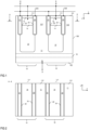
- Figure 1 shows a vertical cross sectional view of one section of a superjunction transistor device. More specifically, Figure 1 shows a vertical cross sectional view of a semiconductor body 100 in which active regions of the superjunction transistor device are integrated.
- the semiconductor body 100 has a first surface 101, which may also be referred to as first main surface.
- Figure 1 shows the semiconductor body 100 in a vertical section plane, wherein this vertical section plane is essentially perpendicular to the first surface 101.
- the semiconductor body 100 may include a conventional semiconductor material, such as, for example, silicon (Si), silicon carbide (SiC), gallium nitride (GaN), gallium arsenide (GaAs), or the like.
- the transistor device includes a drift region 11 of a first doping type (conductivity type) and a plurality of transistor cells 10, wherein in Figure 1 two of the transistor cells 10 are illustrated.
- Each of these transistor cells 10 includes two trench electrodes, a first trench electrode 21, and a second trench electrode 23.
- the first trench electrode 21 is arranged in a first trench and is dielectrically insulated from the semiconductor body 100 by a first dielectric layer 22, which is briefly referred to as first dielectric in the following.
- the second trench electrode 23 is arranged in a second trench and is dielectrically insulated from the semiconductor body 100 by a second dielectric layer 24, which is briefly referred to as second dielectric in the following.
- Each of the first trench and the second trench extends from the first surface 101 into the semiconductor body 100.
- the first trench electrode 21 and the second trench electrode 23 are spaced apart from each other in a first lateral direction x, wherein the first lateral direction x is essentially parallel to the first surface 101 of the semiconductor body 100.
- a region of the semiconductor body 100 between the first trench and the second trench is referred to as first mesa region 111 in the following.
- Each transistor cell 10 further includes a compensation region 12 of the second doping type (conductivity type), a source region 13 of a second doping type complementary to the first doping type, and a body region 14 of the second doping type.
- the source region 13 and the body region 14 are arranged between the first trench and the second trench, that is, each of the source region 13 and the body region 14 is arranged in the first mesa region 111.
- the body region 14 is arranged between the source region 13 and the compensation region 12 and separates the source region 13 from the compensation region 12.
- the body region 14 adjoins both the first dielectric 22 and the second dielectric 24, and the source region 12 adjoins both the first dielectric 22 and the second dielectric 24.
- the compensation region 12 adjoins the body region 14.
- One portion of the compensation region 12 is arranged in the first mesa region 111, that is, between the first and second trench and adjoins the first and second trench.
- a further portion of the compensation region 12, in a vertical direction z of the semiconductor body 100, extends beyond bottoms of the first and second trenches towards a second surface 102 of the semiconductor body 100 and adjoins the at least one drift region 11 so that a pn junction is formed between the compensation region 12 and the drift region 11.
- the "vertical direction" z of the semiconductor body 100 is a direction perpendicular to the first surface 101 of the semiconductor body 100.
- the second surface 102 of the second semiconductor is opposite the first surface 101 and is spaced apart from the first surface 101 in the vertical direction z of the semiconductor body 100.
- the first and second trenches are spaced apart from the second surface 102 and both the drift region 11 and the compensation regions 12 extend beyond bottoms of the trenches towards the second surface 102.
- a vertical dimension of the compensation regions 12 below the trench bottoms is at least 80%, at least 90%, or at least 95% of a vertical dimension of the drift region 11 below the trench bottoms.
- the drift region 11 of the transistor device is connected to a drain node D.
- the transistor device further includes a drain region 15 (illustrated in dashed line) of the first doping type, wherein the drain region 15 is either connected to the drain node D or forms the drain node D of the transistor device.
- a doping concentration of the drain region 15 is higher than a doping concentration of the drift region 11.
- the drift region 11 may adjoin the drain region 15.
- a buffer region 16 of the first doping type is arranged between the drift region 11 and the drain region 15, wherein the buffer region 16 has a doping concentration that is different from the doping concentration of the drift region 11 and lower than a doping concentration of the drain region 15.
- the doping concentration of the buffer region 16 is lower than the doping concentration of the drift region 11.
- the buffer region 16 can be spaced apart from the compensation regions 12 (as illustrated), so that a section of the drift region 11 is arranged between the compensation regions 12 and the buffer region 16, or the buffer region 16 may adjoin the compensation regions 12 (not illustrated).
- the drift region 11 is a continuous semiconductor region that adjoins each of the plurality of compensation regions 12.
- the drift region 11 includes a plurality of drift region sections, wherein each of these drift region sections may be arranged between two compensation regions 12.
- first trench electrode 21 and the second trench electrode 23 of each transistor cell 10 At least the first trench electrode 21 is connected to the gate node G.
- the source regions 13 and the body regions 14 of the transistor cells are connected to the source node S.
- the second trench electrode 23 is connected to the gate node G, is connected to the source node S, or is floating. This is explained in detail herein further below.
- the transistor device can be implemented as an n-type transistor device or as a p-type transistor device.
- the drift region 11, the source regions 13, the optional drain region 15 and the optional buffer region 16 are n-type (n-doped) regions and the compensation regions 12 and the body regions 14 are p-type (p-doped) regions.
- the doping types of the individual active device regions 11-16 are complementary to the doping types in an n-type transistor device.
- the semiconductor body 100 includes monocrystalline silicon and the individual active device regions are implemented such that a respective doping concentration is in a range as outlined in the following:
- the superjunction transistor device which may also be referred to as superjunction MOSFET, can be operated in the same way as a conventional superjunction transistor device.
- the transistor device conducts a current between the drain node D and the source node S when a voltage (drain-source voltage) is applied between a drain node D and the source node S that forward biases the pn junction between the compensation regions 12 of the transistor cells 10 and the drift region 11.
- a voltage drain-source voltage
- the pn junction between the compensation regions 12 and the drift region 11 is forward biases when a positive voltage is applied to the source node S in relation to the drain node D.
- a current flows from the source node S via the body region 14 and the compensation region 12 of each transistor cell 10, and the drift region 11 to the drain node D.
- An operating state of the transistor device in which the pn junctions between the compensation regions 12 and the drift region 11 are forward biased so that a current flows between the source node S and the drain node D is referred to as reverse biased state or reverse conducting state in the following.
- the transistor device When a voltage is applied between the drain node D and the source node S that reverse biases the pn junctions between the drift region 11 and the compensation regions 12 the transistor device can be switched on or switched off by applying a suitable voltage (gate-source voltage) between the gate node G and the source node S.
- the transistor device is in the on-state, when the gate-source voltage is such that a conducting channel is generated by field-effect in the body region 14 and the compensation region 12 along the first dielectric 22, so that a current can flow between the source region 13 and the drift region 11 via this conducting channel along the first dielectric 22.
- the transistor device is in the off-state, when the conducting channel in the body region 14 and the compensation region 12 along the first dielectric 22 is interrupted.
- the off-state when a voltage level of the voltage (drain-source voltage) between the drain node D and the source node S increases, depletion regions (space charge regions) expand in the drift region 11 and the compensation regions 12, wherein these depletion regions further expand as the drain-source voltage increases.
- doping concentrations of the drift region 11 and the compensation regions 12 are such that these regions 11, 12 can completely be depleted of charge carriers.
- the compensation region 12 adjoins the first and second dielectric 22, 24 below the body region 14, so that in the on-state of the transistor device there is a conducting channel along the first dielectric 22 not only in the body region 14 but also the compensation region 12.
- Implementing the compensation region 12 such that it adjoins first and second dielectric 22, 24 may help to improve the short-circuit robustness of the transistor device and offers further degrees of freedom with regard to the design of the overall transistor device.
- the transistor cells 10 are spaced apart from each other in the first lateral direction x, so that a second mesa region 112 is arranged between two neighboring transistor cells 10.
- the second mesa region 112 is arranged between one of the first and second trenches of one of the two neighboring transistor cells 10 and one of the first and second trenches of the other one of the neighboring transistor cells 10.
- the second mesa regions 112 may be implemented in various ways, wherein some examples are explained in the following. It should be noted that the transistor device can be implemented with only one type of second mesa region 112. According to another example, one or more different types of second mesa regions 112 are combined in one transistor device.
- one or more of the second mesa regions 112 include a section of the drift region 11 that extends to the first surface 101.
- the first dielectric 22 is adjacent the drift region section arranged in the second mesa region 112 and is dielectrically insulated from the drift region 11 by the first dielectric 22.
- a transistor device of this type has a relatively high gate-drain-capacitance, which is a capacitance between the gate node G and the drain node D. The gate-drain capacitance influences a switching behavior of the transistor device.
- the gate-drain-capacitance for example, has an effect on how fast the transistor device switches on or off when a voltage level of the gate-source voltage changes, wherein the switching speed decreases as the gate-drain-capacitance increases. Such decrease of the switching speed is desirable in various applications.
- the first trench electrodes 21 are gate electrodes of the transistor device, and the first dielectrics 22 are gate dielectrics.
- the second trench electrodes 23 are connected to the gate node G, are connected to the source node S or are floating. The latter includes that the second trench electrodes are not connected to any terminal having a defined electric potential.
- a second trench electrode 23 connected to the gate node G operates in the same way as the first trench electrode 21 and forms a further gate electrode, so that, in the on-state of the transistor device a conducting channel is generated in the body region 14 and the compensation region 12 along the second dielectric 24. Further, in this case, the second dielectric 24 forms a further gate dielectric.
- the source region 13 may be implemented such that it is spaced apart from the second dielectric 24. That is, the source region 13 may be implemented such that it adjoins the first dielectric 22 (the gate dielectric) but, in the first lateral direction x, does not extend to the second dielectric 24.
- first type transistor cell 10a a transistor cell 10 in which both the first trench electrode 21 and the second trench electrode 23 are connected to the gate node G
- second type transistor cell 10b a transistor cell 10 in which the first trench electrode 21 is connected to the gate node G and the second trench electrode 23 is either connected to the source node S or is floating
- the transistor cells 10 are elongated transistor cells.
- a horizontal cross sectional view of a transistor device of the type shown in Figure 1 that includes elongated transistor cells 10 is shown in Figure 2.
- Figure 2 shows a horizontal cross sectional view of the semiconductor body 100 in a horizontal section plane A-A that cuts through the first and second trench electrodes 21, 23 and the first and second mesa regions 111, 112.
- the elongated transistor cells 10 of the type shown in Figure 2 may also be referred to as stripe cells.
- the first and second trench electrodes 21, 23 are elongated in a second lateral direction y of the semiconductor body 100, wherein the second lateral direction y is essentially perpendicular to the first lateral direction x, in which the first and second trench electrodes 21, 23 are spaced apart from each other.
- “elongated” means that a dimension of the first and second trench electrodes 21, 23 in the second lateral direction y is significantly greater than a dimension of the first and second trench electrodes 21, 23 in the first lateral direction x.
- the dimension of the first and second trench electrodes 21, 23 in the first lateral direction x may also be referred to as width
- the dimension in the second lateral direction y may also be referred to as length.
- the length is at least 100 times, at 1000 times, or at least 10000 times the width.
- a width of the first and second trenches is between 300 nanometers (nm) and 2 micrometers ( ⁇ m), for example.
- Each of the first mesa regions 111 and the second mesa regions 112 has a width, which is a dimension of the respective mesa region 111, 112 in the first lateral direction x.
- the width of the first mesa region 111 is the (shortest) distance between the first trench with the first trench electrode 21 and the second trench with the second trench electrode 23 of one transistor cell 10.
- the width of the second mesa region 112 is the (shortest) distance in the first lateral direction x between the two trenches of neighboring transistor cells that adjoin the mesa region 112.
- the first mesa regions 111 essentially have the same width.
- the second mesa regions 112 may have the same width.
- the widths of the first mesa regions 111 and the widths of the second mesa regions 112 are essentially the same.
- the widths of the first mesa regions 111 and the widths of the second mesa regions 112 are different.
- the widths of the first and second mesa regions are between 300 nanometers (nm) and 5 micrometers ( ⁇ m), in particular between 500 nm and 1 ⁇ m.
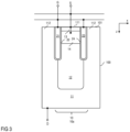
- Figure 3 illustrates one example of a first transistor cell 10a, that is, a transistor cell in which both the first trench electrode 21 and the second trench electrode 23 are connected to the gate node.
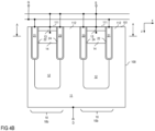
- Figure 4A illustrates one example of a section of the transistor device in which two second type transistor cells 10b are arranged.
- the second type transistor cells 10b are orientated such that the first trench of one of the two transistor cells 10b and the second trench of the other one of the two transistor cells 10b adjoin the mesa region 112 arranged between the two transistor cells 10b.
- the second type transistor cells 10b are orientated such that, form the two second type transistor cells 10b, the second trenches 23 adjoin the second mesa region 112 arranged between the two transistor cells 10b.
- the second type transistor cells 10b are orientated such that the first trenches adjoin the mesa region 112 arranged between the two transistor cells 10b.
- first type transistor cells 10a and the second type transistor cells 10b inside the semiconductor body 100 is identical. Whether a transistor cell 10 is a first type transistor cell 10a or a second type transistor cell 10b is only dependent on where the second trench electrode 21 is connected to.
- the second trench electrode 22 is connected to the gate node G, so that both the first trench electrode 21 and the second trench electrode 23 are connected to the gate node G.
- the second trench electrode 22 is connected to the source node S and the first trench electrode 21 is connected to the gate node G.
- the gate-drain capacitance of the transistor device can be adjusted.
- the semiconductor bodies of various kinds of transistor devices can be manufactured in the same way, wherein the properties of the transistor device, such as the gate-drain capacitance, can be adjusted by suitably wiring the first and second trench electrodes 21, 23 using at least one metallization layer (that is, one or more metallization layers) formed on top of the first surface 101. Examples for wiring the first and second trench electrodes 21, 23 are explained herein further below.
- the transistor device in addition to at least one of the first type transistor cells 10a and the second type transistor cells 10b, may include at least one third type transistor cell 10c.
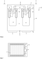
- a third type transistor cell 10c is illustrated in Figure 5 .
- the first trench electrode 21 and the second trench electrode 23 are connected to the source node S or are floating. It is also possible that one of the first trench electrode 21 and the second trench electrode 23 is connected to the source node S and the other one of the first trench electrode 21 and the second trench electrode 23 is floating.
- the third type transistor cell 10c may include a source region 13 (because whether or not the transistor cell is a third type transistor cell is only dependent on which of the gate node G and the source node S, the first and second trench electrodes 21, 23 are connected to).
- the transistor device may include (i) only first type transistor cells, (ii) only second type transistor cells, or (iii) both first type transistor cells and second transistor cells.
- the transistor device includes a source metallization 31.
- the source metallization 31 is formed on top of an insulation layer 32, wherein the insulation layer 32 is formed on top of the first surface 101 of the semiconductor body 100.
- the source metallization 31 is connected to the source node S or forms the source node S of the transistor device.
- electrically conducting vias 33 extend from the metallization layer 31 through the insulation layer 32 to the semiconductor body 100 or into the semiconductor body 100 and are electrically connected to the source regions 13 and the body regions 14 of the individual transistor cells 10. "Electrically connected” in this case may include that the electrically conducting vias 33 are ohmically connected to the source regions 13 and the body regions 14. While a doping concentration of the source regions 13 may be high enough to form an ohmic contact between the source regions 13 and the conducting vias 33, a doping concentration of the body regions 14 may be too low to form such ohmic contacts.
- the body regions 14 may include contact regions 17 of the second doping type, wherein these contact regions 17 adjoin the electrically conducting vias 33 and have a doping concentration that is high enough to form ohmic contacts between the body regions 14 and the electrically conducting vias 33.
- the electrically conducting vias 33 may be elongated in the second lateral direction y.
- the source region 13 and the body region 14 of one transistor cell 10 may be connected to the source metallization 31 by two or more contact vias that are spaced apart from each other in the second lateral direction y.
- Figure 7 shows a top view of one example of a transistor device of the type shown in Figure 6.
- Figure 7 shows a top view of the overall transistor device, wherein the position of the first trench electrodes 21 in the semiconductor body 100 are illustrated in dotted lines.
- the first trench electrodes 21 are elongated trench electrodes, wherein at least one lateral end of these trench electrodes 21 extends beyond the source metallization 31. In a region of this at least one lateral end, each first trench electrodes 21 is electrically connected to a gate runner 41.
- the gate runner 41 is spaced apart from the source metallization 31 and is electrically connected to a gate pad 41.
- the gate pad 41 forms the gate node G of the transistor device or is connected to the gate node G.
- the first trench electrodes 21, in the vertical direction z, are arranged below the gate runner 41 and are electrically connected to the gate runner 41 by electrically conducting vias.
- the position of these vias is schematically illustrated by black dots in the example shown in Figure 7 .
- each first trench electrode 21 may extend beyond the source metallization 31. That is, one lateral end may extend beyond the source metallization 31 and be connected to the gate runner.
- the first trench electrodes 21 may extend beyond the source metallization 31 on opposite ends, so that each first trench electrode 21 has a first end and an opposite second end connected to the gate runner 41.
- the second trench electrodes 23 are not illustrated. Second trench electrodes 23 that are connected to the gate node G may be connected to the gate runner 41 in the same way as the first trench electrodes 21 illustrated in Figure 7 . Connecting the second trench electrodes 23 to the source metallization 31 in second type transistor cells 10b or third type transistor cells can be achieved in the same way as connecting the source and body regions 13, 14 to the source metallization 31.
- Figure 8 shows one example of a second type transistor cell 10b in greater detail.
- the second trench electrode 23 is connected to the source metallization 31 through a further electrically conducting via 34.
- This further electrically conducting via 34 extends from the source metallization 31 through the insulation layer 32 to the second trench electrode 23.
- Figure 9 shows a modification of the transistor device shown in Figure 1 .
- a doped region 51 of the second doping type is arranged in at least one of the second mesa regions 112.
- each of the second mesa regions 112 includes a doped region 51 of the second doping type.
- less than each of the second mesa regions 112 includes a doped region 51 of the second doping type, wherein the remainder of the second mesa regions 112 may be implemented as explained with reference to Figure 6 .
- one second mesa region 112 includes several doped regions 51 of the second doping type, wherein these several doped regions 51 of the second doping type are spaced apart from each other in the second lateral direction y, wherein a respective section of the drift region 11 is arranged between two neighboring doped regions 51 of the second doping type.
- a vertical dimension (depths) of the at least one doped region 51 of the second doping type essentially equals the vertical dimension (depths) of the body regions 14.
- the "vertical dimension" is the dimension in the vertical direction z.
- a doping concentration of the doped region 51 of the second doping type essentially equals the doping concentration of the body regions 14.
- the doped region 51 of the second doping type is electrically connected to the source node S.
- An electrical connection between the doped region 51 and the source node S is schematically illustrated in dashed lines in Figure 9 .
- the doped region 51 of the second doping type which may also be referred to as diode region
- the drift region 11 form a diode between the source node S and the drain node D.
- the transistor device may include a contact region 52 of the second doping type.
- the contact region 52 adjoins the doped region 51, is connected to the source node S and has a doping concentration that is high enough in order to achieve an ohmic contact between the contact region 52 and the source node S.
- the diode region 51 and the optional contact region 52 may be connected to the source node S in the same way as the body regions 14. That is, in a transistor device that includes a source metallization of the type shown in Figure 6 , the diode region 51 may be connected to the source metallization through an electrically conducting via.
- the at least one diode region 51 adjoins the drift region 11, so that a pn junction is formed between the diode region 51 and the drift region 11. Thus, a diode is formed between the source node S and the drain node D by the diode region 51 and the drift region 11.
- the doped region 51 of the second doping type is floating. That is, this region is not electrically connected to the source node S.
- the contact region 52 may be omitted in this case.
- FIG 10 shows a modification of the transistor device shown in Figure 9 .
- a Schottky metal 61 is formed on top of the second mesa regions 112 (as illustrated) or in the second mesa regions 112 (not illustrated), wherein the Schottky metal 61 is electrically connected to the source node S.
- a Schottky contact is formed between the Schottky metal layer 61 and the drift region 11 in the second mesa regions 112, so that a Schottky diode is formed between the drain node D and the source node S of the transistor device.
- This Schottky diode may have a lower forward voltage than a body diode formed by the body regions 14, the compensation regions 12 and the drift region 11.
- the Schottky diode 61 may conduct a reverse current and keep the drain-source voltage on a voltage level that is too low for the body diode to conduct. In this way, the generation of a charge carrier plasma that includes first type charge carriers (electrons or holes) and second type charge carriers (holes or electrons) may be prevented. This may be useful with regard to reducing switching losses of the transistor device.
- Figure 11 shows a further modification of the transistor device shown in Figure 1 .
- the drift region 11 in the second mesa regions 112 is electrically connected to a further circuit node Q of the transistor device.
- This further circuit node Q is also referred to as bias node in the following.
- the drift region 11 may be connected to the bias node Q via a contact region 71 of the first doping type, wherein a doping concentration of this contact region 71 is high enough to provide an ohmic contact between the drift region 11 and the bias node Q.
- the transistor device shown in Figure 11 includes four terminals or circuit nodes, the gate node G, the drain node D, the source node S, and the bias node Q.
- a circuit symbol of this transistor device is shown in Figure 12 .
- This circuit symbol is based on the circuit symbol of a MOSFET and additionally includes the bias node Q.
- the transistor device is an n-type transistor device.
- the body diode in the reverse operating state of the transistor device, the body diode may become forward biased so that, in the reverse direction of the transistor device, a current flows between the source node S and the drain node D.
- Forward biasing the body diode includes generating a charge carrier plasma with first and second type charge carriers in the drift region 11 and the compensation regions 12.
- this charge carrier plasma is removed from the semiconductor body 100 and an internal output capacitance of the transistor device is charged. Removing the charge carrier plasma and charging the output capacitance is associated with a current, which may also be referred to as discharging current. This discharging current is associated with losses.
- the discharging current may flow via a current path across which a supply voltage of the half-bridge is available.
- This supply voltage may be in the range of several hundred volts, such as 400 V, in power converter applications, so that losses associated with removing the charge carrier plasma may be significant.
- the bias node Q can be used to provide a discharging current path that offers lower switching losses.
- a series circuit with a bias voltage source that provides a bias voltage V DEP and a switch SW DEP may be connected between the bias node Q and the source node S.
- the bias voltage V DEP reverse biases the pn junctions between the drift region 11 and the compensation region 12 and the switch SW DEP and the bias voltage source form a current path for removing the charge carrier plasma (and a large share of the output charges associated with charging the output capacitance).
- the bias voltage V DEP is between 5 V and 30 V, for example, and, according to one example, is significantly lower than a voltage blocking capability of the transistor device.
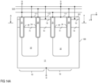
- Figure 14A shows a vertical cross sectional view of a superjunction transistor device according to another example.
- the source regions 13 and the body regions 14 are arranged in the second mesa regions 112.
- the compensation regions 12 are either directly connected to the source node S or are connected to the source node S via connection regions 71 of the second doping type.
- a doping concentration and a depth (in the vertical direction) of these connection regions 71 may correspond to a depth and a doping concentration of the body regions 14.
- the connection regions 71 or the compensation region 12 are ohmically connected to the source node S.
- each of the transistor cells 10 includes a section of the second mesa region 112.
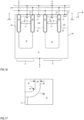
- FIG 14B shows a modification of the transistor device shown in Figure 14A .
- This transistor device is a combination of the transistor device shown in Figure 1 and the transistor device shown in Figure 14A and includes the source regions 13 and the body regions 14 in both the first mesa regions 111 and the second mesa regions 112.
- transistor cells are formed in both the first and second mesa regions 111, 112, wherein the transistor cells in the second mesa regions 112 have a shorter channel length than the transistor cells in the first mesa regions.
- the channel length of a transistor cell in the second mesa regions 112 is essentially given by a shortest distance between the source regions 13 and the drift region 11 along the gate dielectric 21.
- the channel length of a transistor cell in the first mesa regions 112 is essentially given by a length of a path along the gate dielectric 21 from the source region 13 through the body region 14 and the compensation region 12 to the drift region 11.
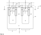
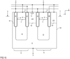
- Figure 15 shows a modification of the transistor device shown in Figure 14A .
- the transistor device shown in Figure 15 is a depletion transistor. That is, the drift region 11, in the second mesa regions 112, adjoins the source region 13 and source regions in the first mesa regions 111 are omitted.
- a doped region 62 of the first doping type that has a doping concentration that is different from the doping concentration of the drift region 11 is arranged in the second mesa regions 112 between the drift region 11 and the source region 13. By suitably selecting the doping concentration of this doped region 62, the pinch-off voltage of the transistor device can be adjusted.
- Figure 16 shows a modification of the transistor device shown in Figure 15 .
- the transistor device shown in Figure 16 includes both depletion transistor cells of the type illustrated in Figure 15 and transistor cells of the type illustrated in Figure 1 .
- the source region 13 in the second mesa 112 may also be electrically connected to a further circuit node Q.
- the conducting channel in the on-state of the transistor device, is formed along the gate dielectric in the body region 14 and the compensation region 12.
- the "gate dielectric” is the first dielectric 22 and, when the second trench electrode 23 is connected to the gate node G, also the second dielectric 24.
- the compensation region 12 may adjoin sidewalls and bottoms of the trenches with the first and second trench electrodes 21, 23.
- the conducting channel, in the compensation region 12 is formed along a corner of the gate dielectric formed between a sidewall and a bottom of the respective trench.
- the gate dielectric is a first dielectric 22 in this example.
- the gate dielectric 22 in order to prevent a voltage breakdown at the corner and in order to prevent that the conducting channel has a locally increased resistance in the region of the corner, has a rounded corner 22'.
- an inner radius r22 of the gate dielectric 22 in the corner region 22' is at least 50% of a thickness d22 of the gate dielectric 22, r22 > 0.5*d22.
- the "inner radius” is the radius of the gate dielectric 22 in a region where the gate dielectric 22 adjoins the gate electrode (first trench electrode) 21.
- the inner radius r22 at least equals the thickness d22 of the gate dielectric 22, r22 > d22.
- the inner radius is between 0.5 times and 3 times the thickness d22, for example, that is 0.5*d22 ⁇ r22 ⁇ 3*d22.
- a rounded corner of the gate dielectric 22 can be achieved by suitably etching the trench before forming the gate dielectric 22 and/or by a suitable process for forming the gate dielectric 22.
- the gate dielectric is a thermally grown oxide.
Landscapes
- Metal-Oxide And Bipolar Metal-Oxide Semiconductor Integrated Circuits (AREA)
- Junction Field-Effect Transistors (AREA)
Claims (15)
- Transistorbauelement, das aufweist:einen Halbleiterkörper (100);ein Driftgebiet (11) in dem Halbleiterkörper (100);mehrere Transistorzellen (10); undeinen Gateknoten (G) und einen Sourceknoten (S);wobei jede der mehreren Transistorzellen (10) aufweist:eine erste Grabenelektrode (21), die von dem Halbleiterkörper (100) durch eine erste dielektrische Schicht (22) isoliert ist;eine zweite Grabenelektrode (23), die von dem Halbleiterkörper (100) durch eine zweite dielektrische Schicht (24) isoliert ist;ein Sourcegebiet (13) und ein Bodygebiet (14) in einem ersten Mesagebiet (111) zwischen der ersten Grabenelektrode (21) und der zweiten Grabenelektrode (23); undein Kompensationsgebiet (12),wobei das Kompensationsgebiet (12) an das Bodygebiet (14), die erste dielektrische Schicht (22) und die zweite dielektrische Schicht (24) angrenzt,wobei das Driftgebiet (11) ein Gebiet eines ersten Dotierungstyps ist und das Kompensationsgebiet (12) ein Gebiet eines zu dem ersten Dotierungstyp komplementären zweiten Dotierungstyps ist und einen pn-Übergang mit dem Driftgebiet (11) bildet, undwobei von der ersten Grabenelektrode (21) und der zweiten Grabenelektrode (23) wenigstens die erste Grabenelektrode (21) an den Gateknoten (G) angeschlossen ist.
- Transistorbauelement nach Anspruch 1,
wobei die mehreren Transistorzellen (10) wenigstens eine Transistorzelle (10a) eines ersten Typs aufweisen, in der die erste Grabenelektrode (21) an den Gateknoten (G) angeschlossen ist und die zweite Grabenelektrode (23) an den Gateknoten (G) angeschlossen ist. - Transistorbauelement nach Anspruch 1 oder 2,
wobei die mehreren Transistorzellen (10) wenigstens eine Transistorzelle (10b) eines zweiten Typs aufweisen, in der die erste Grabenelektrode (21) an den Gateknoten (G) angeschlossen ist und die zweite Grabenelektrode (23) an den Sourceknoten (S) angeschlossen ist. - Transistorbauelement nach Anspruch 2 oder 3,
wobei die mehreren Transistorzellen (10) wenigstens eine Transistorzelle (10c) eines dritten Typs aufweisen, in der die erste Grabenelektrode (21) an den Sourceknoten (S) angeschlossen ist und die zweite Grabenelektrode (23) an den Sourceknoten (S) angeschlossen ist. - Transistorbauelement nach einem der vorhergehenden Ansprüche, das ferner aufweist:
mehrere zweite Mesagebiete (112), die jeweils zwischen zwei benachbarten Transistorzellen (10) angeordnet sind und an eine erste Oberfläche (101) des Halbleiterkörpers (100) angrenzen. - Transistorbauelement nach Anspruch 5,
wobei wenigstens eines der mehreren zweiten Mesagebiete (112) einen Abschnitt des Driftgebiets (11) aufweist, der sich zu der ersten Oberfläche (101) erstreckt. - Transistorbauelement nach Anspruch 5 oder 6,
wobei wenigstens eines der mehreren zweiten Mesagebiete (112) ein dotiertes Gebiet (51) aufweist, das einen pn-Übergang mit dem Driftgebiet (11) bildet. - Transistorbauelement nach einem der Ansprüche 5 bis 7, das ferner aufweist:
einen Schottky-Kontakt, der zwischen dem Sourceknoten (S) und dem Driftgebiet (11) in wenigstens einem der zweiten Mesagebiete (112) gebildet ist. - Transistorbauelement nach Anspruch 5, das ferner aufweist:einen Vorspannungsknoten (Q), der sich von dem Sourceknoten (S) unterscheidet,wobei der Vorspannungsknoten (Q) an das Driftgebiet (11) in dem zweiten Mesagebiet (112) angeschlossen ist.
- Transistorbauelement nach einem der vorhergehenden Ansprüche, das ferner aufweist:
ein Draingebiet (15), das an einen Drainknoten (D) angeschlossen ist oder einen Drainknoten (D) des Transistorbauelements bildet. - Transistorbauelement nach einem der vorhergehenden Ansprüche,
wobei wenigstens die erste dielektrische Schicht (22) eine abgerundete Ecke (22') in einem Gebiet aufweist, in dem die erste dielektrische Schicht (22) an das Kompensationsgebiet (12) angrenzt. - Transistorbauelement nach Anspruch 11, wobei ein Innenradius (r22) der abgerundeten Ecke zwischen dem 0,5-fachen und dem 3-fachen einer Dicke (d22) der ersten dielektrischen Schicht (22) beträgt.
- Elektronische Schaltung, die aufweist:ein Transistorbauelement nach einem der Ansprüche 9 bis 12; undeinen elektronischen Schalter (SWDEP) und eine Vorspannungsquelle, die zwischen dem Sourceknoten (S) und dem Vorspannungsknoten (Q) in Reihe geschaltet sind.
- Transistorbauelement, das aufweist:einen Halbleiterkörper (100);ein Driftgebiet (11) in dem Halbleiterkörper (100);mehrere Transistorzellen (10); undeinen Gateknoten (G) und einen Sourceknoten (S);wobei jede der mehreren Transistorzellen (10) aufweist:eine erste Grabenelektrode (21), die von dem Halbleiterkörper (100) durch eine erste dielektrische Schicht (22) isoliert ist;eine zweite Grabenelektrode (23), die von dem Halbleiterkörper (100) durch eine zweite dielektrische Schicht (24) isoliert ist;ein Sourcegebiet (13) und ein Bodygebiet (14); undein Kompensationsgebiet (12),wobei das Kompensationsgebiet (12) an die erste dielektrische Schicht (22) und die zweite dielektrische Schicht (24) in einem ersten Mesagebiet (111) zwischen der ersten Grabenelektrode (21) und der zweiten Grabenelektrode (22) angrenzt,wobei das Driftgebiet (11) ein Gebiet eines ersten Dotierungstyps ist und das Kompensationsgebiet (12) ein Gebiet eines zu dem ersten Dotierungstyp komplementären zweiten Dotierungstyps ist und einen pn-Übergang mit dem Driftgebiet (11) bildet,wobei von der ersten Grabenelektrode (21) und der zweiten Grabenelektrode (23) wenigstens die erste Grabenelektrode (21) an den Gateknoten (G) angeschlossen ist, undwobei das Sourcegebiet (13) und das Bodygebiet (14) in einem zweiten Mesagebiet (112) angeordnet sind, das sich von dem ersten Mesagebiet (111) unterscheidet, wobei das zweite Mesagebiet (112) an die erste Grabenelektrode (21) angrenzt.
- Transistorbauelement nach Anspruch 14, wobei wenigstens eine der Transistorzellen (10) ferner ein Sourcegebiet (13) und ein Bodygebiet (14) in dem ersten Mesagebiet (111) aufweist.
Applications Claiming Priority (3)
| Application Number | Priority Date | Filing Date | Title |
|---|---|---|---|
| PCT/EP2020/051245 WO2020182357A1 (en) | 2019-03-08 | 2020-01-20 | Method for operating a superjunction transistor device and superjunction transistor device |
| EP20194876 | 2020-09-07 | ||
| PCT/EP2021/051023 WO2021148383A1 (en) | 2020-01-20 | 2021-01-19 | Superjunction transistor device |
Publications (2)
| Publication Number | Publication Date |
|---|---|
| EP4094359A1 EP4094359A1 (de) | 2022-11-30 |
| EP4094359B1 true EP4094359B1 (de) | 2024-12-18 |
Family
ID=76992080
Family Applications (1)
| Application Number | Title | Priority Date | Filing Date |
|---|---|---|---|
| EP21704398.3A Active EP4094359B1 (de) | 2020-01-20 | 2021-01-19 | Verfahren zum betrieb einer superjunction-transistorvorrichtung |
Country Status (3)
| Country | Link |
|---|---|
| US (1) | US12490485B2 (de) |
| EP (1) | EP4094359B1 (de) |
| WO (1) | WO2021148383A1 (de) |
Family Cites Families (9)
| Publication number | Priority date | Publication date | Assignee | Title |
|---|---|---|---|---|
| US7615847B2 (en) * | 2007-03-23 | 2009-11-10 | Infineon Technologies Austria Ag | Method for producing a semiconductor component |
| JP5612256B2 (ja) * | 2008-10-16 | 2014-10-22 | 株式会社東芝 | 半導体装置 |
| WO2011087994A2 (en) * | 2010-01-12 | 2011-07-21 | Maxpower Semiconductor Inc. | Devices, components and methods combining trench field plates with immobile electrostatic charge |
| US8803205B2 (en) * | 2011-05-31 | 2014-08-12 | Infineon Technologies Austria Ag | Transistor with controllable compensation regions |
| US9166028B2 (en) * | 2011-05-31 | 2015-10-20 | Infineon Technologies Austria Ag | Circuit configured to adjust the activation state of transistors based on load conditions |
| US9893175B2 (en) * | 2013-09-30 | 2018-02-13 | Infineon Technologies Austria Ag | Integrated circuit with a power transistor and a driver circuit integrated in a common semiconductor body |
| DE102016113183B4 (de) * | 2016-07-18 | 2021-02-11 | Infineon Technologies Austria Ag | Leistungshalbleitervorrichtung mit einer Feldelektrode und Schaltleistungsvorrichtung |
| CN208570614U (zh) * | 2018-08-16 | 2019-03-01 | 无锡新洁能股份有限公司 | 一种绝缘栅双极型半导体器件 |
| EP3706314B1 (de) * | 2019-03-08 | 2022-10-19 | Infineon Technologies Austria AG | Verfahren zum betrieb einer superjunction-transistorvorrichtung |
-
2021
- 2021-01-19 US US17/792,447 patent/US12490485B2/en active Active
- 2021-01-19 EP EP21704398.3A patent/EP4094359B1/de active Active
- 2021-01-19 WO PCT/EP2021/051023 patent/WO2021148383A1/en not_active Ceased
Also Published As
| Publication number | Publication date |
|---|---|
| EP4094359A1 (de) | 2022-11-30 |
| US12490485B2 (en) | 2025-12-02 |
| WO2021148383A1 (en) | 2021-07-29 |
| US20230126534A1 (en) | 2023-04-27 |
Similar Documents
| Publication | Publication Date | Title |
|---|---|---|
| US12283621B2 (en) | Semiconductor device having a transistor with trenches and mesas | |
| US9087707B2 (en) | Semiconductor arrangement with a power transistor and a high voltage device integrated in a common semiconductor body | |
| US8110868B2 (en) | Power semiconductor component with a low on-state resistance | |
| US7238576B2 (en) | Semiconductor device and method of manufacturing the same | |
| US9825129B2 (en) | Transistor device | |
| CN104576737B (zh) | 半导体器件 | |
| WO2003046996A1 (en) | Vertical mosfets having crossing trench-based gate electrodes that extend into deeper trench-based source electrodes and methods of forming same | |
| CN104103691B (zh) | 具有补偿区的半导体器件 | |
| KR20000015138A (ko) | 트렌치 절연 게이트 바이폴라 트랜지스터 | |
| CN104979401A (zh) | 半导体器件和集成电路 | |
| EP1026750A1 (de) | Feldeffekttransistoren mit isolierter Steuerelektrode | |
| US20160343848A1 (en) | Transistor Arrangement Including Power Transistors and Voltage Limiting Means | |
| US20120126317A1 (en) | Accufet with integrated clamping circuit | |
| EP1291925B1 (de) | Halbleitervorrichtung | |
| CN112670333A (zh) | 窄半导体台面器件 | |
| US20200185494A1 (en) | Semiconductor Device and Method for Producing a Semiconductor Device | |
| US12490485B2 (en) | Superjunction transistor device | |
| EP3716340A1 (de) | Transistorvorrichtung | |
| JP2009512207A (ja) | パワー半導体デバイス | |
| US11682696B2 (en) | Semiconductor device having a high breakdown voltage | |
| US11682695B2 (en) | Semiconductor device having a high breakdown voltage |
Legal Events
| Date | Code | Title | Description |
|---|---|---|---|
| STAA | Information on the status of an ep patent application or granted ep patent |
Free format text: STATUS: UNKNOWN |
|
| STAA | Information on the status of an ep patent application or granted ep patent |
Free format text: STATUS: THE INTERNATIONAL PUBLICATION HAS BEEN MADE |
|
| PUAI | Public reference made under article 153(3) epc to a published international application that has entered the european phase |
Free format text: ORIGINAL CODE: 0009012 |
|
| STAA | Information on the status of an ep patent application or granted ep patent |
Free format text: STATUS: REQUEST FOR EXAMINATION WAS MADE |
|
| 17P | Request for examination filed |
Effective date: 20220714 |
|
| AK | Designated contracting states |
Kind code of ref document: A1 Designated state(s): AL AT BE BG CH CY CZ DE DK EE ES FI FR GB GR HR HU IE IS IT LI LT LU LV MC MK MT NL NO PL PT RO RS SE SI SK SM TR |
|
| DAV | Request for validation of the european patent (deleted) | ||
| DAX | Request for extension of the european patent (deleted) | ||
| GRAP | Despatch of communication of intention to grant a patent |
Free format text: ORIGINAL CODE: EPIDOSNIGR1 |
|
| STAA | Information on the status of an ep patent application or granted ep patent |
Free format text: STATUS: GRANT OF PATENT IS INTENDED |
|
| INTG | Intention to grant announced |
Effective date: 20240730 |
|
| GRAS | Grant fee paid |
Free format text: ORIGINAL CODE: EPIDOSNIGR3 |
|
| GRAA | (expected) grant |
Free format text: ORIGINAL CODE: 0009210 |
|
| STAA | Information on the status of an ep patent application or granted ep patent |
Free format text: STATUS: THE PATENT HAS BEEN GRANTED |
|
| AK | Designated contracting states |
Kind code of ref document: B1 Designated state(s): AL AT BE BG CH CY CZ DE DK EE ES FI FR GB GR HR HU IE IS IT LI LT LU LV MC MK MT NL NO PL PT RO RS SE SI SK SM TR |
|
| P01 | Opt-out of the competence of the unified patent court (upc) registered |
Free format text: CASE NUMBER: APP_60562/2024 Effective date: 20241111 |
|
| REG | Reference to a national code |
Ref country code: CH Ref legal event code: EP |
|
| REG | Reference to a national code |
Ref country code: DE Ref legal event code: R096 Ref document number: 602021023521 Country of ref document: DE |
|
| REG | Reference to a national code |
Ref country code: IE Ref legal event code: FG4D |
|
| REG | Reference to a national code |
Ref country code: LT Ref legal event code: MG9D |
|
| PG25 | Lapsed in a contracting state [announced via postgrant information from national office to epo] |
Ref country code: HR Free format text: LAPSE BECAUSE OF FAILURE TO SUBMIT A TRANSLATION OF THE DESCRIPTION OR TO PAY THE FEE WITHIN THE PRESCRIBED TIME-LIMIT Effective date: 20241218 |
|
| PG25 | Lapsed in a contracting state [announced via postgrant information from national office to epo] |
Ref country code: FI Free format text: LAPSE BECAUSE OF FAILURE TO SUBMIT A TRANSLATION OF THE DESCRIPTION OR TO PAY THE FEE WITHIN THE PRESCRIBED TIME-LIMIT Effective date: 20241218 |
|
| PG25 | Lapsed in a contracting state [announced via postgrant information from national office to epo] |
Ref country code: BG Free format text: LAPSE BECAUSE OF FAILURE TO SUBMIT A TRANSLATION OF THE DESCRIPTION OR TO PAY THE FEE WITHIN THE PRESCRIBED TIME-LIMIT Effective date: 20241218 |
|
| PG25 | Lapsed in a contracting state [announced via postgrant information from national office to epo] |
Ref country code: NO Free format text: LAPSE BECAUSE OF FAILURE TO SUBMIT A TRANSLATION OF THE DESCRIPTION OR TO PAY THE FEE WITHIN THE PRESCRIBED TIME-LIMIT Effective date: 20250318 |
|
| REG | Reference to a national code |
Ref country code: NL Ref legal event code: MP Effective date: 20241218 |
|
| PG25 | Lapsed in a contracting state [announced via postgrant information from national office to epo] |
Ref country code: LV Free format text: LAPSE BECAUSE OF FAILURE TO SUBMIT A TRANSLATION OF THE DESCRIPTION OR TO PAY THE FEE WITHIN THE PRESCRIBED TIME-LIMIT Effective date: 20241218 Ref country code: GR Free format text: LAPSE BECAUSE OF FAILURE TO SUBMIT A TRANSLATION OF THE DESCRIPTION OR TO PAY THE FEE WITHIN THE PRESCRIBED TIME-LIMIT Effective date: 20250319 |
|
| PG25 | Lapsed in a contracting state [announced via postgrant information from national office to epo] |
Ref country code: RS Free format text: LAPSE BECAUSE OF FAILURE TO SUBMIT A TRANSLATION OF THE DESCRIPTION OR TO PAY THE FEE WITHIN THE PRESCRIBED TIME-LIMIT Effective date: 20250318 |
|
| PG25 | Lapsed in a contracting state [announced via postgrant information from national office to epo] |
Ref country code: NL Free format text: LAPSE BECAUSE OF FAILURE TO SUBMIT A TRANSLATION OF THE DESCRIPTION OR TO PAY THE FEE WITHIN THE PRESCRIBED TIME-LIMIT Effective date: 20241218 |
|
| REG | Reference to a national code |
Ref country code: AT Ref legal event code: MK05 Ref document number: 1753067 Country of ref document: AT Kind code of ref document: T Effective date: 20241218 |
|
| PG25 | Lapsed in a contracting state [announced via postgrant information from national office to epo] |
Ref country code: SM Free format text: LAPSE BECAUSE OF FAILURE TO SUBMIT A TRANSLATION OF THE DESCRIPTION OR TO PAY THE FEE WITHIN THE PRESCRIBED TIME-LIMIT Effective date: 20241218 |
|
| PG25 | Lapsed in a contracting state [announced via postgrant information from national office to epo] |
Ref country code: PL Free format text: LAPSE BECAUSE OF FAILURE TO SUBMIT A TRANSLATION OF THE DESCRIPTION OR TO PAY THE FEE WITHIN THE PRESCRIBED TIME-LIMIT Effective date: 20241218 |
|
| PG25 | Lapsed in a contracting state [announced via postgrant information from national office to epo] |
Ref country code: ES Free format text: LAPSE BECAUSE OF FAILURE TO SUBMIT A TRANSLATION OF THE DESCRIPTION OR TO PAY THE FEE WITHIN THE PRESCRIBED TIME-LIMIT Effective date: 20241218 |
|
| PG25 | Lapsed in a contracting state [announced via postgrant information from national office to epo] |
Ref country code: IS Free format text: LAPSE BECAUSE OF FAILURE TO SUBMIT A TRANSLATION OF THE DESCRIPTION OR TO PAY THE FEE WITHIN THE PRESCRIBED TIME-LIMIT Effective date: 20250418 |
|
| PG25 | Lapsed in a contracting state [announced via postgrant information from national office to epo] |
Ref country code: PT Free format text: LAPSE BECAUSE OF FAILURE TO SUBMIT A TRANSLATION OF THE DESCRIPTION OR TO PAY THE FEE WITHIN THE PRESCRIBED TIME-LIMIT Effective date: 20250421 |
|
| PG25 | Lapsed in a contracting state [announced via postgrant information from national office to epo] |
Ref country code: EE Free format text: LAPSE BECAUSE OF FAILURE TO SUBMIT A TRANSLATION OF THE DESCRIPTION OR TO PAY THE FEE WITHIN THE PRESCRIBED TIME-LIMIT Effective date: 20241218 |
|
| PG25 | Lapsed in a contracting state [announced via postgrant information from national office to epo] |
Ref country code: RO Free format text: LAPSE BECAUSE OF FAILURE TO SUBMIT A TRANSLATION OF THE DESCRIPTION OR TO PAY THE FEE WITHIN THE PRESCRIBED TIME-LIMIT Effective date: 20241218 Ref country code: AT Free format text: LAPSE BECAUSE OF FAILURE TO SUBMIT A TRANSLATION OF THE DESCRIPTION OR TO PAY THE FEE WITHIN THE PRESCRIBED TIME-LIMIT Effective date: 20241218 |
|
| PG25 | Lapsed in a contracting state [announced via postgrant information from national office to epo] |
Ref country code: SK Free format text: LAPSE BECAUSE OF FAILURE TO SUBMIT A TRANSLATION OF THE DESCRIPTION OR TO PAY THE FEE WITHIN THE PRESCRIBED TIME-LIMIT Effective date: 20241218 |
|
| PG25 | Lapsed in a contracting state [announced via postgrant information from national office to epo] |
Ref country code: CZ Free format text: LAPSE BECAUSE OF FAILURE TO SUBMIT A TRANSLATION OF THE DESCRIPTION OR TO PAY THE FEE WITHIN THE PRESCRIBED TIME-LIMIT Effective date: 20241218 |
|
| PG25 | Lapsed in a contracting state [announced via postgrant information from national office to epo] |
Ref country code: IT Free format text: LAPSE BECAUSE OF FAILURE TO SUBMIT A TRANSLATION OF THE DESCRIPTION OR TO PAY THE FEE WITHIN THE PRESCRIBED TIME-LIMIT Effective date: 20241218 |
|
| REG | Reference to a national code |
Ref country code: CH Ref legal event code: PL |
|
| PG25 | Lapsed in a contracting state [announced via postgrant information from national office to epo] |
Ref country code: SE Free format text: LAPSE BECAUSE OF FAILURE TO SUBMIT A TRANSLATION OF THE DESCRIPTION OR TO PAY THE FEE WITHIN THE PRESCRIBED TIME-LIMIT Effective date: 20241218 |
|
| PG25 | Lapsed in a contracting state [announced via postgrant information from national office to epo] |
Ref country code: LU Free format text: LAPSE BECAUSE OF NON-PAYMENT OF DUE FEES Effective date: 20250119 Ref country code: MC Free format text: LAPSE BECAUSE OF FAILURE TO SUBMIT A TRANSLATION OF THE DESCRIPTION OR TO PAY THE FEE WITHIN THE PRESCRIBED TIME-LIMIT Effective date: 20241218 |
|
| REG | Reference to a national code |
Ref country code: DE Ref legal event code: R097 Ref document number: 602021023521 Country of ref document: DE |
|
| PG25 | Lapsed in a contracting state [announced via postgrant information from national office to epo] |
Ref country code: DK Free format text: LAPSE BECAUSE OF FAILURE TO SUBMIT A TRANSLATION OF THE DESCRIPTION OR TO PAY THE FEE WITHIN THE PRESCRIBED TIME-LIMIT Effective date: 20241218 |
|
| PG25 | Lapsed in a contracting state [announced via postgrant information from national office to epo] |
Ref country code: BE Free format text: LAPSE BECAUSE OF NON-PAYMENT OF DUE FEES Effective date: 20250131 |
|
| PG25 | Lapsed in a contracting state [announced via postgrant information from national office to epo] |
Ref country code: CH Free format text: LAPSE BECAUSE OF NON-PAYMENT OF DUE FEES Effective date: 20250131 |
|
| REG | Reference to a national code |
Ref country code: BE Ref legal event code: MM Effective date: 20250131 |
|
| PLBE | No opposition filed within time limit |
Free format text: ORIGINAL CODE: 0009261 |
|
| STAA | Information on the status of an ep patent application or granted ep patent |
Free format text: STATUS: NO OPPOSITION FILED WITHIN TIME LIMIT |
|
| 26N | No opposition filed |
Effective date: 20250919 |
|
| GBPC | Gb: european patent ceased through non-payment of renewal fee |
Effective date: 20250318 |
|
| PG25 | Lapsed in a contracting state [announced via postgrant information from national office to epo] |
Ref country code: GB Free format text: LAPSE BECAUSE OF NON-PAYMENT OF DUE FEES Effective date: 20250318 |
|
| PG25 | Lapsed in a contracting state [announced via postgrant information from national office to epo] |
Ref country code: FR Free format text: LAPSE BECAUSE OF NON-PAYMENT OF DUE FEES Effective date: 20250218 |
|
| PG25 | Lapsed in a contracting state [announced via postgrant information from national office to epo] |
Ref country code: IE Free format text: LAPSE BECAUSE OF NON-PAYMENT OF DUE FEES Effective date: 20250119 |
|
| PGFP | Annual fee paid to national office [announced via postgrant information from national office to epo] |
Ref country code: DE Payment date: 20260323 Year of fee payment: 6 |