EP4092756A2 - High electron mobility transistor and manufacturing method thereof - Google Patents
High electron mobility transistor and manufacturing method thereof Download PDFInfo
- Publication number
- EP4092756A2 EP4092756A2 EP22184384.0A EP22184384A EP4092756A2 EP 4092756 A2 EP4092756 A2 EP 4092756A2 EP 22184384 A EP22184384 A EP 22184384A EP 4092756 A2 EP4092756 A2 EP 4092756A2
- Authority
- EP
- European Patent Office
- Prior art keywords
- layer
- hole
- forming
- supply
- supply layer
- Prior art date
- Legal status (The legal status is an assumption and is not a legal conclusion. Google has not performed a legal analysis and makes no representation as to the accuracy of the status listed.)
- Pending
Links
Images



Classifications
-
- H—ELECTRICITY
- H10—SEMICONDUCTOR DEVICES; ELECTRIC SOLID-STATE DEVICES NOT OTHERWISE PROVIDED FOR
- H10D—INORGANIC ELECTRIC SEMICONDUCTOR DEVICES
- H10D30/00—Field-effect transistors [FET]
- H10D30/40—FETs having zero-dimensional [0D], one-dimensional [1D] or two-dimensional [2D] charge carrier gas channels
- H10D30/47—FETs having zero-dimensional [0D], one-dimensional [1D] or two-dimensional [2D] charge carrier gas channels having two-dimensional [2D] charge carrier gas channels, e.g. nanoribbon FETs or high electron mobility transistors [HEMT]
- H10D30/471—High electron mobility transistors [HEMT] or high hole mobility transistors [HHMT]
- H10D30/472—High electron mobility transistors [HEMT] or high hole mobility transistors [HHMT] having lower bandgap active layer formed on top of wider bandgap layer, e.g. inverted HEMT
-
- H—ELECTRICITY
- H10—SEMICONDUCTOR DEVICES; ELECTRIC SOLID-STATE DEVICES NOT OTHERWISE PROVIDED FOR
- H10D—INORGANIC ELECTRIC SEMICONDUCTOR DEVICES
- H10D30/00—Field-effect transistors [FET]
- H10D30/40—FETs having zero-dimensional [0D], one-dimensional [1D] or two-dimensional [2D] charge carrier gas channels
- H10D30/47—FETs having zero-dimensional [0D], one-dimensional [1D] or two-dimensional [2D] charge carrier gas channels having two-dimensional [2D] charge carrier gas channels, e.g. nanoribbon FETs or high electron mobility transistors [HEMT]
-
- H—ELECTRICITY
- H10—SEMICONDUCTOR DEVICES; ELECTRIC SOLID-STATE DEVICES NOT OTHERWISE PROVIDED FOR
- H10D—INORGANIC ELECTRIC SEMICONDUCTOR DEVICES
- H10D30/00—Field-effect transistors [FET]
- H10D30/01—Manufacture or treatment
- H10D30/015—Manufacture or treatment of FETs having heterojunction interface channels or heterojunction gate electrodes, e.g. HEMT
-
- H—ELECTRICITY
- H10—SEMICONDUCTOR DEVICES; ELECTRIC SOLID-STATE DEVICES NOT OTHERWISE PROVIDED FOR
- H10D—INORGANIC ELECTRIC SEMICONDUCTOR DEVICES
- H10D30/00—Field-effect transistors [FET]
- H10D30/40—FETs having zero-dimensional [0D], one-dimensional [1D] or two-dimensional [2D] charge carrier gas channels
- H10D30/47—FETs having zero-dimensional [0D], one-dimensional [1D] or two-dimensional [2D] charge carrier gas channels having two-dimensional [2D] charge carrier gas channels, e.g. nanoribbon FETs or high electron mobility transistors [HEMT]
- H10D30/471—High electron mobility transistors [HEMT] or high hole mobility transistors [HHMT]
- H10D30/475—High electron mobility transistors [HEMT] or high hole mobility transistors [HHMT] having wider bandgap layer formed on top of lower bandgap active layer, e.g. undoped barrier HEMTs such as i-AlGaN/GaN HEMTs
-
- H—ELECTRICITY
- H10—SEMICONDUCTOR DEVICES; ELECTRIC SOLID-STATE DEVICES NOT OTHERWISE PROVIDED FOR
- H10D—INORGANIC ELECTRIC SEMICONDUCTOR DEVICES
- H10D62/00—Semiconductor bodies, or regions thereof, of devices having potential barriers
- H10D62/10—Shapes, relative sizes or dispositions of the regions of the semiconductor bodies; Shapes of the semiconductor bodies
- H10D62/13—Semiconductor regions connected to electrodes carrying current to be rectified, amplified or switched, e.g. source or drain regions
- H10D62/149—Source or drain regions of field-effect devices
- H10D62/151—Source or drain regions of field-effect devices of IGFETs
-
- H—ELECTRICITY
- H10—SEMICONDUCTOR DEVICES; ELECTRIC SOLID-STATE DEVICES NOT OTHERWISE PROVIDED FOR
- H10D—INORGANIC ELECTRIC SEMICONDUCTOR DEVICES
- H10D62/00—Semiconductor bodies, or regions thereof, of devices having potential barriers
- H10D62/10—Shapes, relative sizes or dispositions of the regions of the semiconductor bodies; Shapes of the semiconductor bodies
- H10D62/17—Semiconductor regions connected to electrodes not carrying current to be rectified, amplified or switched, e.g. channel regions
- H10D62/351—Substrate regions of field-effect devices
- H10D62/357—Substrate regions of field-effect devices of FETs
- H10D62/364—Substrate regions of field-effect devices of FETs of IGFETs
- H10D62/378—Contact regions to the substrate regions
-
- H—ELECTRICITY
- H10—SEMICONDUCTOR DEVICES; ELECTRIC SOLID-STATE DEVICES NOT OTHERWISE PROVIDED FOR
- H10D—INORGANIC ELECTRIC SEMICONDUCTOR DEVICES
- H10D62/00—Semiconductor bodies, or regions thereof, of devices having potential barriers
- H10D62/80—Semiconductor bodies, or regions thereof, of devices having potential barriers characterised by the materials
- H10D62/85—Semiconductor bodies, or regions thereof, of devices having potential barriers characterised by the materials being Group III-V materials, e.g. GaAs
- H10D62/8503—Nitride Group III-V materials, e.g. AlN or GaN
-
- H—ELECTRICITY
- H10—SEMICONDUCTOR DEVICES; ELECTRIC SOLID-STATE DEVICES NOT OTHERWISE PROVIDED FOR
- H10D—INORGANIC ELECTRIC SEMICONDUCTOR DEVICES
- H10D64/00—Electrodes of devices having potential barriers
- H10D64/20—Electrodes characterised by their shapes, relative sizes or dispositions
- H10D64/23—Electrodes carrying the current to be rectified, amplified, oscillated or switched, e.g. sources, drains, anodes or cathodes
- H10D64/251—Source or drain electrodes for field-effect devices
-
- H—ELECTRICITY
- H10—SEMICONDUCTOR DEVICES; ELECTRIC SOLID-STATE DEVICES NOT OTHERWISE PROVIDED FOR
- H10D—INORGANIC ELECTRIC SEMICONDUCTOR DEVICES
- H10D64/00—Electrodes of devices having potential barriers
- H10D64/20—Electrodes characterised by their shapes, relative sizes or dispositions
- H10D64/23—Electrodes carrying the current to be rectified, amplified, oscillated or switched, e.g. sources, drains, anodes or cathodes
- H10D64/251—Source or drain electrodes for field-effect devices
- H10D64/256—Source or drain electrodes for field-effect devices for lateral devices wherein the source or drain electrodes are recessed in semiconductor bodies
-
- H—ELECTRICITY
- H10—SEMICONDUCTOR DEVICES; ELECTRIC SOLID-STATE DEVICES NOT OTHERWISE PROVIDED FOR
- H10D—INORGANIC ELECTRIC SEMICONDUCTOR DEVICES
- H10D64/00—Electrodes of devices having potential barriers
- H10D64/20—Electrodes characterised by their shapes, relative sizes or dispositions
- H10D64/27—Electrodes not carrying the current to be rectified, amplified, oscillated or switched, e.g. gates
- H10D64/311—Gate electrodes for field-effect devices
- H10D64/411—Gate electrodes for field-effect devices for FETs
- H10D64/511—Gate electrodes for field-effect devices for FETs for IGFETs
-
- H—ELECTRICITY
- H10—SEMICONDUCTOR DEVICES; ELECTRIC SOLID-STATE DEVICES NOT OTHERWISE PROVIDED FOR
- H10D—INORGANIC ELECTRIC SEMICONDUCTOR DEVICES
- H10D62/00—Semiconductor bodies, or regions thereof, of devices having potential barriers
- H10D62/80—Semiconductor bodies, or regions thereof, of devices having potential barriers characterised by the materials
- H10D62/85—Semiconductor bodies, or regions thereof, of devices having potential barriers characterised by the materials being Group III-V materials, e.g. GaAs
- H10D62/854—Semiconductor bodies, or regions thereof, of devices having potential barriers characterised by the materials being Group III-V materials, e.g. GaAs further characterised by the dopants
-
- H—ELECTRICITY
- H10—SEMICONDUCTOR DEVICES; ELECTRIC SOLID-STATE DEVICES NOT OTHERWISE PROVIDED FOR
- H10D—INORGANIC ELECTRIC SEMICONDUCTOR DEVICES
- H10D64/00—Electrodes of devices having potential barriers
- H10D64/20—Electrodes characterised by their shapes, relative sizes or dispositions
- H10D64/27—Electrodes not carrying the current to be rectified, amplified, oscillated or switched, e.g. gates
- H10D64/311—Gate electrodes for field-effect devices
- H10D64/411—Gate electrodes for field-effect devices for FETs
- H10D64/511—Gate electrodes for field-effect devices for FETs for IGFETs
- H10D64/512—Disposition of the gate electrodes, e.g. buried gates
- H10D64/513—Disposition of the gate electrodes, e.g. buried gates within recesses in the substrate, e.g. trench gates, groove gates or buried gates
Definitions
- the present invention relates to a high-electron-mobility field-effect transistor (HEMT) and a method for manufacturing the HEMT transistor.
- the present invention relates to an HEMT transistor with high stress resilience during OFF-state.
- High electron-mobility field-effect transistors based on the formation of layers of high-mobility two-dimensional electron gas (2DEG) at a heterojunction, i.e. the interface between semiconductor materials with different band gaps, are known.
- HEMT transistors based on a heterojunction between a layer of aluminium nitride and gallium (AlGaN) and a layer of gallium nitride (GaN) are known.
- HEMT transistors based on AlGaN/GaN heterojunctions offer various advantages that make same particularly suitable and widely used in a range of different applications.
- the high breakdown threshold of the HEMT transistors is used by high-performance power switches; the high mobility of the electrons in the conductive channel makes it possible to build high-frequency amplifiers.
- the high concentration of electrons in the 2DEG makes it possible to achieve low ON-state resistance (R ON ).
- HEMT transistors based on AlGaN/GaN heterojunctions are usually made by growing GaN and AlGaN layers on silicon substrates. Consequently, HEMT transistors built in this manner are planar, i.e. having source, gate and drain electrodes that are aligned on a plane parallel to the substrate.
- the potential drop V DS_OFF between the source electrode and the drain electrode in OFF-state conditions of the HEMT transistors may reach several hundreds of volts, depending on the power supply voltage. Consequently, a malfunction mechanism in the HEMT transistors is caused by the formation of high electrical fields, and consequent breakdown, in the region between the gate electrode and the drain electrode in OFF-state conditions. As a result, the breakdown threshold of the HEMT transistor is an important figure of merit of the HEMT transistor.
- a known problem in known HEMT transistors relates to an increase in the ON-state resistance R ON as a result of the stress caused by the high voltage V DS_OFF in OFF-state.
- Said reversible increase in R ON can be attributed to a range of factors, including emission/capture phenomena inside trap states in a buffer layer of the HEMT transistor.
- the buffer layer emits holes as a function of the quantity of trap states, going on to form a layer of negative charges inside same. This layer of negative charges causes a partial emptying of the 2DEG, which thus increases the ON-state resistance R ON .
- the breakdown threshold of the HEMT transistor can be increased by increasing the distance between the gate electrode and the drain electrode of the HEMT transistor, thereby reducing the electrical field for the same power supply voltage.
- this solution also causes an unwanted increase in the ON-state resistance R ON .
- the purpose of the present invention is to provide an HEMT transistor and a related manufacturing method that address the drawbacks in the prior art.
- the present invention provides for an HEMT transistor and a method for manufacturing the HEMT transistor, as defined in the attached claims.
- Figure 1 shows, in a system of three axes X, Y, Z that are orthogonal to one another, a side view in the plane XZ of an HEMT device 1 based on an AlGaN/GaN heterojunction.
- the HEMT device 1 includes a substrate 2, a buffer layer 4 arranged on the substrate 2, a hole-supply layer 6 arranged on the buffer layer 4, and a heterojunction or heterostructure 7 arranged on the hole-supply layer 6.
- one or more additional buffer layers (or interface layers) (not shown) made from compounds of the group III-V of the periodic table, including gallium, are arranged between the substrate 2 and the buffer layer 4.
- the one or more interface layers are designed to maintain the drain voltage when the device is powered off and to reduce the density of threading dislocations, and therefore of trap states.
- the substrate 2 is for example made of silicon or silicon carbide (SiC) or sapphire (Al 2 O 3 ), or GaN.
- the buffer layer 4 is made of intrinsic or N-type doped gallium nitride, and has a high concentration of carbon impurities, for example a concentration of between 10 16 and 10 19 cm -3 , in order to attenuate the vertical leakage towards the substrate 2.
- the hole-supply layer 6 is made of P-type doped gallium nitride, for example using magnesium (Mg) with a concentration of between 10 17 and 3 ⁇ 10 19 cm -3 .
- Mg magnesium
- the heterostructure 7 in particular includes a channel layer 10 arranged on top of the buried layer 6, and a barrier layer 9 arranged on top of the channel layer 10.
- the channel layer 10 is made of intrinsic gallium nitride (GaN).
- the barrier layer 9 is made of aluminium nitride and gallium (AlGaN) with a thickness of between 10 nm and 30 nm.
- the channel layer 10 and the barrier layer 9 are generally made of materials that, when coupled together as shown in Figure 1 , form a heterojunction that enables the formation of a two-dimensional gas layer (2DEG).
- the HEMT device 1 also includes an insulating layer 12 arranged on the heterostructure 7.
- the insulating layer 12 is made of dielectric material, for example silicon nitride (Si 3 N 4 ) or silicon dioxide (SiO 2 ) and has a thickness of between 5 nm and 100 nm.
- the semiconductor body 15 contains an active region 15a that is the active portion of the HEMT device 1.
- the HEMT device 1 also includes a gate region 14 arranged between source region 16 and drain region 18.
- the active region 15a is arranged laterally (i.e. along the axis X) between the source region 16 and the drain region 18.
- the active region 15a extends depthwise (i.e. along the axis Z) into the layers of the semiconductor body 15 in which the gate region 14, the source region 16 and the drain region 18 are arranged.
- the gate region 14 is separated laterally from the source region 16 and the drain region 18 by respective portions of the insulating layer 12.
- the gate region 14 extends depthwise through the insulating layer 12 and into the heterostructure 7, ending at the interface between the barrier layer 9 and the channel layer 10.
- the gate region 14 is formed in a trench 19 hollowed out of part of the semiconductor body 15, the depth of which is the same as the depth of the gate region 14.
- a dielectric layer 11 made of insulating material, such as silicon dioxide, is arranged on the insulating layer 12 and inside the trench 19, partially filling the trench 19 and forming a gate dielectric layer 14a inside the trench 19.
- the gate dielectric layer 14a is arranged on the bottom and on the inner side walls of the trench 19.
- a gate metallization 14b is arranged in the trench 19 on the gate dielectric layer 14a, completely filling the trench 19.
- the gate dielectric layer 14a and the gate metallization 14b form the gate region 14 of the HEMT device 1.
- the source region 16 which is made of conductive material such as titanium (Ti) or aluminium (Al), extends across the insulating layer 12 and the heterostructure 7, ending inside the hole-supply layer 6.
- the drain region 18, which is made of conductive material such as titanium (Ti) or aluminium (Al), extends across the insulating layer 12, ending at the interface between the insulating layer 12 and the barrier layer 9. According to another embodiment not shown in the figures, the drain region 18 may be recessed, i.e. penetrate a portion of the semiconductor body 15 beneath the interface between the insulating layer 12 and the barrier layer 9.
- the HEMT device 1 is a normally-off device, hence the need to bias the gate region 14 with a voltage V G greater than a threshold voltage V th to generate a conductive channel between the source region 16 and the drain region 18.
- V G a voltage greater than a threshold voltage V th
- V th a threshold voltage
- the value of the current I DS between the source region 16 and the drain region 18 depends on the concentration of electrons in the 2DEG at the interface between the barrier layer 9 and the channel layer 10.
- the buffer layer 4 has trap states, for example due to the high concentration of impurities therein.
- the buffer layer 4 emits holes as a function of the quantity of trap states, going on to form a layer of negative charges inside same. This layer of negative charges causes a reduction in the concentration of electrons in the 2DEG.
- the HEMT transistor 1 when the HEMT transistor is in OFF-state, there is a high voltage V DS_OFF between the source region 16 and the drain region 18.
- the stress caused by the voltage V DS_OFF in OFF-state generates further trap states inside the buffer layer 4.
- the hole-supply layer 6 has a high concentration of P-type impurities, and is therefore a source of holes to replace the holes emitted by the buffer layer 4 and to neutralize the layer of negative charges inside same.
- the source region 16 extends up to the hole-supply layer 6, biasing same such as to facilitate the transport of holes from the hole-supply layer 6 to the buffer layer 4. Consequently, following the stress caused by the voltage V DS_OFF in OFF-state, the HEMT transistor 1 is not subject to an increase in ON-state resistance R ON .
- the neutralization mechanism for the layer of negative charges inside the buffer layer 4 can be optimized by appropriately selecting a thickness t p of the hole-supply layer 6, a thickness t u of the channel layer 10 and a surface concentration N A of dopant species of the hole-supply layer 6.
- the thickness t p of the hole-supply layer 6 is preferably determined using the following equation: t p > ⁇ t u + t u 2 + 2 ⁇ B qN A + 2 ⁇ E A qN A where q is the elementary charge (approximately 1.6 ⁇ 10 -19 C); B is the band gap of the material of the buffer layer 4; E A is the distance in the band diagram between the trap states, for example generated by the presence of carbon atoms, and the valence band of the buffer layer (4); and ⁇ is the dielectric constant of the material of the hole-supply layer 6.
- E A can be determined using known methods provided in the literature, for example in A. Chini et al., "Experimental and Numerical Analysis of Hole Emission Process From Carbon-Related Traps in GaN Buffer Layers", Trans. Elec. Dev., 63(9), pages 3473-3478, 2016 .
- the hole-supply layer 6 may have a thickness of between 10 nm and 1 ⁇ m and a concentration of active dopant species of between 10 17 cm -2 and 10 19 cm -2 , while the channel layer 10 may have a thickness of between 10 nm and 1 ⁇ m.
- FIG. 2 shows a normally-on HEMT transistor 21 according to another aspect of the present disclosure. Elements of the HEMT transistor 21 in Figure 2 that are common with the HEMT transistor 1 in Figure 1 are identified using the same reference signs and are not further described. With reference to Figure 2 , the gate region 14 extends depthwise into the insulating layer 12, ending at the interface between the insulating layer 12 and the barrier layer 9. Consequently, unlike the HEMT transistor 1 in Figure 1 , the gate region 14 does not extend into the barrier layer 9.
- Figure 3 shows a normally-off HEMT transistor 31 according to another aspect of the present disclosure. Elements of the HEMT transistor 31 in Figure 3 that are common with the HEMT transistor 1 in Figure 1 are identified using the same reference signs and are not further described. With reference to Figure 3 , the gate region 14 extends across the insulating layer 12, the heterostructure 7, the hole-supply layer 6 and part of the buffer layer 4, ending inside the buffer layer 4.
- the buffer layer 4 of p-GaN is partially interrupted by the trench of the gate region 14.
- a conductive channel 32 (shown schematically using arrows) is created between the source region 16 and the drain region 18 that extends along the axis Z through the hole-supply layer 6 and along the axis X through the buffer layer 4, beneath the gate region 14. This ensures that the path of the current through the p-GaN hole-supply layer 6 is minimized and the ON-state resistance R ON is further optimized.
- Figure 4A is a cross section of a portion of a wafer 40 during a manufacturing step of the HEMT device 1. Elements of the wafer 40 that are common with the subject matter described with reference to Figure 1 and shown in Figure 1 are indicated using the same reference signs.
- the wafer 40 including the substrate 2, which is for example made of silicon (Si) or silicon carbide (SiC) or aluminium oxide (Al 2 O 3 ), with a front side 2a and a rear side 2b arranged opposite one another in a direction Z, and the buffer layer 4, which is made of intrinsic or N-type doped gallium nitride (GaN), the lower side 4a of which is arranged on the front side 2a of the substrate 2 (additional interface layers not shown in the figure may also be included).
- the substrate 2 is for example made of silicon (Si) or silicon carbide (SiC) or aluminium oxide (Al 2 O 3 )
- the buffer layer 4 which is made of intrinsic or N-type doped gallium nitride (GaN)
- GaN gallium nitride
- the hole-supply layer 6 made of P-type doped gallium nitride (GaN) is then formed, for example using epitaxial growth.
- the thickness t p of the hole-supply layer 6 is between 10 nm and 1 ⁇ m, determined on the basis of the equation (1) given above.
- the heterostructure 7 is then formed.
- the channel layer 10 made of intrinsic gallium nitride (GaN) is formed, for example using epitaxial growth.
- the thickness t u of the channel layer 10 is between 10 nm and 1 ⁇ m, determined on the basis of the equation (1) given above.
- the barrier layer 9 made of aluminium nitride and gallium (AlGaN) is then formed, for example using epitaxial growth.
- the thickness of the barrier layer 9 is between 10 nm and 30 nm.
- the exposed upper side of the barrier layer 9 forms a front side 7a of the heterostructure 7.
- the insulating layer 12 which is made of an insulating or dielectric material such as silicon nitride (SiN), silicon oxide (SiO 2 ), nickel oxide (NiO) or another material, is then formed on the front side 7a of the heterostructure 7.
- the insulating layer 12 has a thickness of between 5 nm and 300 nm, for example 100 nm, and is formed by chemical vapour deposition (CVD) or atomic layer deposition (ALD).
- the insulating layer 12 is then selectively removed, for example using lithography and etching steps, such as to remove selected portions of same in the region of the wafer 40 where the gate region 14 is to be formed in successive steps (or in a portion of the active area 15a).
- etching step is then carried out on the barrier layer 9, using the same lithography mask as the etching step for the insulating layer 12. Etching is terminated once the interface with the channel layer 10 has been reached. This forms a trench 19. Alternatively, in a manner not shown in the figures, the etching step for the barrier layer 9 is not carried out, in order to manufacture the HEMT transistor 21 in Figure 2 .
- the etching step of the barrier layer 9 is followed by an etching step of the channel layer 10, an etching step of the hole-supply layer 6 and an etching step of the buffer layer 4, using the same lithography mask as for the etching step of the insulating layer 12, in order to manufacture the HEMT transistor 31 in Figure 3 .
- the channel layer 10 and the hole-supply layer 6 are completely removed in the selected portions defined by the lithography mask of the etching step of the insulating layer 12, the etching of the buffer layer 4 terminating inside same, before reaching the interface with the substrate 2.
- a deposition or growth step of the gate dielectric layer 14a for example made of a material selected from aluminium nitride (AlN), silicon nitride (SiN), aluminium oxide (Al 2 O 3 ) and silicon oxide (SiO 2 ), is then carried out.
- the thickness of the gate dielectric layer 14a is selected to be between 5 nm and 50 nm.
- a first aperture 60a and a second aperture 60b are formed on opposite sides, along X, of the gate region 14, and away from the gate region 14.
- the first aperture 60a extends depthwise through the insulating layer 12 and the heterostructure 7, ending inside the hole-supply layer 6.
- the second aperture 60b extends depthwise through the insulating layer 12, ending at the interface between the insulating layer 12 and the barrier layer 9.
- the second aperture 60b may penetrate a portion of the semiconductor body 15 beneath the interface between the insulating layer 12 and the barrier layer 9.
- an ohmic-contact formation step is then carried out to form the source region 16 and the drain region 18, depositing conductive material, in particular metal such as titanium (Ti) or aluminium (Al), or alloys or compounds thereof, using sputter or evaporator and a photolithographic mask for lift-off, inside the apertures 60a, 60b.
- the conductive material completely fills the apertures 60a, 60b, forming the source region 16 and the drain region 18 respectively.
- a rapid thermal annealing (RTA) step is carried out, for example at a temperature of between approximately 500°C and 800°C for a time of between 30 seconds and 2 minutes.
- a deposition step of conductive material on the wafer 40 is then carried out to form the gate metallization 14b on the gate dielectric layer 14a, in particular completely filling the trench 19.
- the gate metallization 14b is made of a metal material such as tantalum (Ta), tantalum nitride (TaN), titanium nitride (TiN), palladium (Pa), tungsten (W), tungsten silicide (WSi 2 ), titanium aluminium (Ti/Al), nickel gold (Ni/Au).
- the gate metallization 14b is deposited selectively in the trench 19 and at a distance between the source region 16 and the drain region 18 using lithography steps which are known per se.
- the gate metallization 14b and the gate dielectric layer 14a together form the recessed gate region 14 of the HEMT device 1 in Figure 1 .
- the HEMT device 1 shown in Figure 1 is thus formed.
- FIG. 5 shows a normally-off HEMT transistor 51 according to an embodiment of the present invention. Elements of the HEMT transistor 51 in Figure 5 that are common with the HEMT transistor 1 in Figure 1 are identified using the same reference signs and are not further described.
- the HEMT transistor 51 includes a gate region 54 arranged on the insulating layer 12 between the source region 16 and a drain region 58, and is separated from said regions.
- the drain region 58 which is made of conductive material such as titanium (Ti) or aluminium (Al), extends across the insulating layer 12 and the barrier layer 9, ending at the interface between the barrier layer 9 and the channel layer 10.
- the HEMT transistor 51 also includes a buried region 56 of P-type doped gallium nitride extending in the gate region 54, depthwise through the insulating layer 12, ending at the interface between the insulating layer 12 and the barrier layer 9.
- the structure formed by the gate region 54 and by the buried region 56 is known in the prior art as a "p-GaN gate” and an HEMT transistor containing such a structure is known as a "p-GaN gate transistor".
- the present invention makes it possible to nullify the effect of stress on R ON without reducing the breakdown threshold value and without increasing the value of R ON before the stress.
- the metallization of the contacts (source, drain, gate) on the front of the wafer can be carried out using any variants known in the literature, such as the formation of contacts using AlSiCu/Ti, Al/Ti, or W-plug, and the like.
- the buffer layer 4, the hole-supply layer 6 and the heterostructure 7 can be made of other materials selected from compound materials in the group III-V.
Landscapes
- Junction Field-Effect Transistors (AREA)
Abstract
Description
- This application claims priority from
Italian Patent Application No. 102017000064155 filed on 09/06/2017 - The present invention relates to a high-electron-mobility field-effect transistor (HEMT) and a method for manufacturing the HEMT transistor. In particular, the present invention relates to an HEMT transistor with high stress resilience during OFF-state.
- High electron-mobility field-effect transistors (HEMT) based on the formation of layers of high-mobility two-dimensional electron gas (2DEG) at a heterojunction, i.e. the interface between semiconductor materials with different band gaps, are known. For example, HEMT transistors based on a heterojunction between a layer of aluminium nitride and gallium (AlGaN) and a layer of gallium nitride (GaN) are known.
- HEMT transistors based on AlGaN/GaN heterojunctions offer various advantages that make same particularly suitable and widely used in a range of different applications. For example, the high breakdown threshold of the HEMT transistors is used by high-performance power switches; the high mobility of the electrons in the conductive channel makes it possible to build high-frequency amplifiers. Furthermore, the high concentration of electrons in the 2DEG makes it possible to achieve low ON-state resistance (RON).
- Due to the high cost of gallium nitride substrates, HEMT transistors based on AlGaN/GaN heterojunctions are usually made by growing GaN and AlGaN layers on silicon substrates. Consequently, HEMT transistors built in this manner are planar, i.e. having source, gate and drain electrodes that are aligned on a plane parallel to the substrate.
- When used in power applications, the potential drop VDS_OFF between the source electrode and the drain electrode in OFF-state conditions of the HEMT transistors may reach several hundreds of volts, depending on the power supply voltage. Consequently, a malfunction mechanism in the HEMT transistors is caused by the formation of high electrical fields, and consequent breakdown, in the region between the gate electrode and the drain electrode in OFF-state conditions. As a result, the breakdown threshold of the HEMT transistor is an important figure of merit of the HEMT transistor.
- Another important figure of merit of the HEMT transistor is the ON-state resistance RON, which should be minimized to save power.
- Furthermore, a known problem in known HEMT transistors relates to an increase in the ON-state resistance RON as a result of the stress caused by the high voltage VDS_OFF in OFF-state. Said reversible increase in RON can be attributed to a range of factors, including emission/capture phenomena inside trap states in a buffer layer of the HEMT transistor. In known HEMT transistors, the buffer layer emits holes as a function of the quantity of trap states, going on to form a layer of negative charges inside same. This layer of negative charges causes a partial emptying of the 2DEG, which thus increases the ON-state resistance RON.
- A range of different solutions for individually optimizing the aforementioned figures of merit of HEMT transistors are known. However, optimizing one figure of merit normally has a negative impact on one or more other figures of merit.
- For example, the breakdown threshold of the HEMT transistor can be increased by increasing the distance between the gate electrode and the drain electrode of the HEMT transistor, thereby reducing the electrical field for the same power supply voltage. However, this solution also causes an unwanted increase in the ON-state resistance RON.
- Another known solution is disclosed in Tanaka, K. et al., "Suppression of current collapse by hole injection from drain in a normally-off GaN-based hybrid-drain-embedded gate injection transistor", Appl. Phys. Lett., 107, 163502 (2015). Said document relates to an HEMT transistor in which a layer of P-type doped gallium nitride (p-GaN) is formed by growth on a barrier layer of aluminium nitride and gallium, and connected to a drain electrode. This transistor has increased RON as a result of the substantially negligible stress in OFF-state (VDS_OFF = 800 V). Nonetheless, an increase in RON is observed in static conditions, regardless of stress.
- It is therefore particularly important to provide a method to prevent RON from increasing as a result of the stress in OFF-state in HEMT transistors that does not have a negative effect on the breakdown threshold.
- The purpose of the present invention is to provide an HEMT transistor and a related manufacturing method that address the drawbacks in the prior art.
- The present invention provides for an HEMT transistor and a method for manufacturing the HEMT transistor, as defined in the attached claims.
- The present invention is further described below with reference to preferred embodiments of same, which are provided purely as non-limiting examples, and to the attached drawings, in which:
-
Figure 1 is a lateral cross section of an HEMT transistor according to one aspect of the present disclosure, -
Figure 2 is a lateral cross section of an HEMT transistor according to another aspect of the present disclosure, -
Figure 3 is a lateral cross section of an HEMT transistor according to another aspect of the present disclosure, -
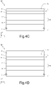
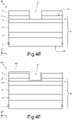
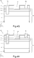
Figures 4A to 4H show manufacturing steps of the HEMT transistor inFigure 1 , and -
Figure 5 is a lateral cross section of an HEMT transistor according to an embodiment of the present invention. -
Figure 1 shows, in a system of three axes X, Y, Z that are orthogonal to one another, a side view in the plane XZ of anHEMT device 1 based on an AlGaN/GaN heterojunction. - The
HEMT device 1 includes asubstrate 2, abuffer layer 4 arranged on thesubstrate 2, a hole-supply layer 6 arranged on thebuffer layer 4, and a heterojunction or heterostructure 7 arranged on the hole-supply layer 6. Optionally, one or more additional buffer layers (or interface layers) (not shown) made from compounds of the group III-V of the periodic table, including gallium, are arranged between thesubstrate 2 and thebuffer layer 4. The one or more interface layers are designed to maintain the drain voltage when the device is powered off and to reduce the density of threading dislocations, and therefore of trap states. - The
substrate 2 is for example made of silicon or silicon carbide (SiC) or sapphire (Al2O3), or GaN. Thebuffer layer 4 is made of intrinsic or N-type doped gallium nitride, and has a high concentration of carbon impurities, for example a concentration of between 1016 and 1019 cm-3, in order to attenuate the vertical leakage towards thesubstrate 2. - The hole-
supply layer 6 is made of P-type doped gallium nitride, for example using magnesium (Mg) with a concentration of between 1017 and 3·1019 cm-3. - The heterostructure 7 in particular includes a
channel layer 10 arranged on top of the buriedlayer 6, and abarrier layer 9 arranged on top of thechannel layer 10. Thechannel layer 10 is made of intrinsic gallium nitride (GaN). Thebarrier layer 9 is made of aluminium nitride and gallium (AlGaN) with a thickness of between 10 nm and 30 nm. Thechannel layer 10 and thebarrier layer 9 are generally made of materials that, when coupled together as shown inFigure 1 , form a heterojunction that enables the formation of a two-dimensional gas layer (2DEG). - The
HEMT device 1 also includes aninsulating layer 12 arranged on the heterostructure 7. Theinsulating layer 12 is made of dielectric material, for example silicon nitride (Si3N4) or silicon dioxide (SiO2) and has a thickness of between 5 nm and 100 nm. - Hereinafter, the
substrate 2, thebuffer layer 4, the hole-supply layer 6 and the heterostructure 7 are referred to as a whole using theterm semiconductor body 15. Thesemiconductor body 15 contains anactive region 15a that is the active portion of theHEMT device 1. - The HEMT
device 1 also includes agate region 14 arranged betweensource region 16 and drainregion 18. Theactive region 15a is arranged laterally (i.e. along the axis X) between thesource region 16 and thedrain region 18. Theactive region 15a extends depthwise (i.e. along the axis Z) into the layers of thesemiconductor body 15 in which thegate region 14, thesource region 16 and thedrain region 18 are arranged. - The
gate region 14 is separated laterally from thesource region 16 and thedrain region 18 by respective portions of theinsulating layer 12. Thegate region 14 extends depthwise through theinsulating layer 12 and into the heterostructure 7, ending at the interface between thebarrier layer 9 and thechannel layer 10. - The
gate region 14 is formed in atrench 19 hollowed out of part of thesemiconductor body 15, the depth of which is the same as the depth of thegate region 14. Adielectric layer 11 made of insulating material, such as silicon dioxide, is arranged on theinsulating layer 12 and inside thetrench 19, partially filling thetrench 19 and forming a gatedielectric layer 14a inside thetrench 19. In particular, the gatedielectric layer 14a is arranged on the bottom and on the inner side walls of thetrench 19. Agate metallization 14b is arranged in thetrench 19 on the gatedielectric layer 14a, completely filling thetrench 19. The gatedielectric layer 14a and thegate metallization 14b form thegate region 14 of theHEMT device 1. - The
source region 16, which is made of conductive material such as titanium (Ti) or aluminium (Al), extends across theinsulating layer 12 and the heterostructure 7, ending inside the hole-supply layer 6. - The
drain region 18, which is made of conductive material such as titanium (Ti) or aluminium (Al), extends across the insulatinglayer 12, ending at the interface between the insulatinglayer 12 and thebarrier layer 9. According to another embodiment not shown in the figures, thedrain region 18 may be recessed, i.e. penetrate a portion of thesemiconductor body 15 beneath the interface between the insulatinglayer 12 and thebarrier layer 9. - The
HEMT device 1 is a normally-off device, hence the need to bias thegate region 14 with a voltage VG greater than a threshold voltage Vth to generate a conductive channel between thesource region 16 and thedrain region 18. When in use, the value of the current IDS between thesource region 16 and thedrain region 18 depends on the concentration of electrons in the 2DEG at the interface between thebarrier layer 9 and thechannel layer 10. Thebuffer layer 4 has trap states, for example due to the high concentration of impurities therein. Thebuffer layer 4 emits holes as a function of the quantity of trap states, going on to form a layer of negative charges inside same. This layer of negative charges causes a reduction in the concentration of electrons in the 2DEG. Furthermore, when the HEMT transistor is in OFF-state, there is a high voltage VDS_OFF between thesource region 16 and thedrain region 18. The stress caused by the voltage VDS_OFF in OFF-state generates further trap states inside thebuffer layer 4. The hole-supply layer 6 has a high concentration of P-type impurities, and is therefore a source of holes to replace the holes emitted by thebuffer layer 4 and to neutralize the layer of negative charges inside same. Thesource region 16 extends up to the hole-supply layer 6, biasing same such as to facilitate the transport of holes from the hole-supply layer 6 to thebuffer layer 4. Consequently, following the stress caused by the voltage VDS_OFF in OFF-state, theHEMT transistor 1 is not subject to an increase in ON-state resistance RON. - The neutralization mechanism for the layer of negative charges inside the
buffer layer 4 can be optimized by appropriately selecting a thickness tp of the hole-supply layer 6, a thickness tu of thechannel layer 10 and a surface concentration NA of dopant species of the hole-supply layer 6. The applicant has verified that, for a given thickness tu of thechannel layer 10 and a given surface concentration NA of dopant species of the hole-supply layer 6, the thickness tp of the hole-supply layer 6 is preferably determined using the following equation:
buffer layer 4; EA is the distance in the band diagram between the trap states, for example generated by the presence of carbon atoms, and the valence band of the buffer layer (4); and ε is the dielectric constant of the material of the hole-supply layer 6. In this embodiment, thebuffer layer 4 is a carbon-doped layer of gallium nitride, for which B = 3.4 eV, EA = 0.9 eV, ε = 9ε0, where ε0 is the dielectric constant of the void. The value of EA can be determined using known methods provided in the literature, for example in A. Chini et al., "Experimental and Numerical Analysis of Hole Emission Process From Carbon-Related Traps in GaN Buffer Layers", Trans. Elec. Dev., 63(9), pages 3473-3478, 2016. - For example, for a concentration NA = 1017 cm-2 of active dopant species in the hole-
supply layer 6 and a thickness tu = 100 nm of thechannel layer 10, it is preferable to select a thickness tp of the hole-supply layer 6 that is greater than 204 nm. More generally, the hole-supply layer 6 may have a thickness of between 10 nm and 1 µm and a concentration of active dopant species of between 1017 cm-2 and 1019 cm-2, while thechannel layer 10 may have a thickness of between 10 nm and 1 µm. -
Figure 2 shows a normally-onHEMT transistor 21 according to another aspect of the present disclosure. Elements of theHEMT transistor 21 inFigure 2 that are common with theHEMT transistor 1 inFigure 1 are identified using the same reference signs and are not further described. With reference toFigure 2 , thegate region 14 extends depthwise into the insulatinglayer 12, ending at the interface between the insulatinglayer 12 and thebarrier layer 9. Consequently, unlike theHEMT transistor 1 inFigure 1 , thegate region 14 does not extend into thebarrier layer 9. - The presence of the
source region 16, arranged in direct electrical contact with the hole-supply layer 6, makes it possible to obtain the same advantages as described above in relation to theHEMT transistor 1. -
Figure 3 shows a normally-off HEMT transistor 31 according to another aspect of the present disclosure. Elements of theHEMT transistor 31 inFigure 3 that are common with theHEMT transistor 1 inFigure 1 are identified using the same reference signs and are not further described. With reference toFigure 3 , thegate region 14 extends across the insulatinglayer 12, the heterostructure 7, the hole-supply layer 6 and part of thebuffer layer 4, ending inside thebuffer layer 4. - In this embodiment, the
buffer layer 4 of p-GaN is partially interrupted by the trench of thegate region 14. This technical solution allows to obtain a turn-on threshold more positive (important for normally-off devices), guarantying in any case the possibility to have a source of holes required to fill-in the traps negatively charged during turning-off of the device. - The presence of the
source region 16, arranged in direct electrical contact with the hole-supply layer 6, makes it possible to obtain the same advantages as described above in relation to theHEMT transistor 1. - During use, when the
gate region 14 is biased with a voltage VG greater than a threshold voltage Vth, a conductive channel 32 (shown schematically using arrows) is created between thesource region 16 and thedrain region 18 that extends along the axis Z through the hole-supply layer 6 and along the axis X through thebuffer layer 4, beneath thegate region 14. This ensures that the path of the current through the p-GaN hole-supply layer 6 is minimized and the ON-state resistance RON is further optimized. - Manufacturing steps of the
HEMT device 1 inFigure 1 are described below with reference toFigures 4A to 4H . -
Figure 4A is a cross section of a portion of awafer 40 during a manufacturing step of theHEMT device 1. Elements of thewafer 40 that are common with the subject matter described with reference toFigure 1 and shown inFigure 1 are indicated using the same reference signs. - In particular and as shown in
Figure 4A , there is arranged thewafer 40 including thesubstrate 2, which is for example made of silicon (Si) or silicon carbide (SiC) or aluminium oxide (Al2O3), with afront side 2a and arear side 2b arranged opposite one another in a direction Z, and thebuffer layer 4, which is made of intrinsic or N-type doped gallium nitride (GaN), thelower side 4a of which is arranged on thefront side 2a of the substrate 2 (additional interface layers not shown in the figure may also be included). - As shown in
Figure 4B , the hole-supply layer 6 made of P-type doped gallium nitride (GaN) is then formed, for example using epitaxial growth. By way of example, the thickness tp of the hole-supply layer 6 is between 10 nm and 1 µm, determined on the basis of the equation (1) given above. - As shown in
Figure 4C , the heterostructure 7 is then formed. In a first step, thechannel layer 10 made of intrinsic gallium nitride (GaN) is formed, for example using epitaxial growth. The thickness tu of thechannel layer 10 is between 10 nm and 1 µm, determined on the basis of the equation (1) given above. Thebarrier layer 9 made of aluminium nitride and gallium (AlGaN) is then formed, for example using epitaxial growth. The thickness of thebarrier layer 9 is between 10 nm and 30 nm. The exposed upper side of thebarrier layer 9 forms afront side 7a of the heterostructure 7. - As shown in
Figure 4D , the insulatinglayer 12, which is made of an insulating or dielectric material such as silicon nitride (SiN), silicon oxide (SiO2), nickel oxide (NiO) or another material, is then formed on thefront side 7a of the heterostructure 7. The insulatinglayer 12 has a thickness of between 5 nm and 300 nm, for example 100 nm, and is formed by chemical vapour deposition (CVD) or atomic layer deposition (ALD). - As shown in
Figure 4E , the insulatinglayer 12 is then selectively removed, for example using lithography and etching steps, such as to remove selected portions of same in the region of thewafer 40 where thegate region 14 is to be formed in successive steps (or in a portion of theactive area 15a). - An etching step is then carried out on the
barrier layer 9, using the same lithography mask as the etching step for the insulatinglayer 12. Etching is terminated once the interface with thechannel layer 10 has been reached. This forms atrench 19. Alternatively, in a manner not shown in the figures, the etching step for thebarrier layer 9 is not carried out, in order to manufacture theHEMT transistor 21 inFigure 2 . Alternatively, in a manner not shown in the figures, the etching step of thebarrier layer 9 is followed by an etching step of thechannel layer 10, an etching step of the hole-supply layer 6 and an etching step of thebuffer layer 4, using the same lithography mask as for the etching step of the insulatinglayer 12, in order to manufacture theHEMT transistor 31 inFigure 3 . In this case, thechannel layer 10 and the hole-supply layer 6 are completely removed in the selected portions defined by the lithography mask of the etching step of the insulatinglayer 12, the etching of thebuffer layer 4 terminating inside same, before reaching the interface with thesubstrate 2. - As shown in
Figure 4F , a deposition or growth step of thegate dielectric layer 14a, for example made of a material selected from aluminium nitride (AlN), silicon nitride (SiN), aluminium oxide (Al2O3) and silicon oxide (SiO2), is then carried out. The thickness of thegate dielectric layer 14a is selected to be between 5 nm and 50 nm. - As shown in
Figure 4G , one or more further mask etching steps are then carried out on thedielectric layer 14a, the insulatinglayer 12 and thesemiconductor body 15 to remove selected portions thereof arranged in regions of thewafer 40 where thesource region 16 and thedrain region 18 of theHEMT device 1 are to be formed. In particular, afirst aperture 60a and asecond aperture 60b are formed on opposite sides, along X, of thegate region 14, and away from thegate region 14. Thefirst aperture 60a extends depthwise through the insulatinglayer 12 and the heterostructure 7, ending inside the hole-supply layer 6. Thesecond aperture 60b extends depthwise through the insulatinglayer 12, ending at the interface between the insulatinglayer 12 and thebarrier layer 9. Alternatively, in a manner not shown in the figures, thesecond aperture 60b may penetrate a portion of thesemiconductor body 15 beneath the interface between the insulatinglayer 12 and thebarrier layer 9. - As shown in
Figure 4H , an ohmic-contact formation step is then carried out to form thesource region 16 and thedrain region 18, depositing conductive material, in particular metal such as titanium (Ti) or aluminium (Al), or alloys or compounds thereof, using sputter or evaporator and a photolithographic mask for lift-off, inside theapertures apertures source region 16 and thedrain region 18 respectively. After deposition, a rapid thermal annealing (RTA) step is carried out, for example at a temperature of between approximately 500°C and 800°C for a time of between 30 seconds and 2 minutes. - A deposition step of conductive material on the
wafer 40 is then carried out to form thegate metallization 14b on thegate dielectric layer 14a, in particular completely filling thetrench 19. For example, thegate metallization 14b is made of a metal material such as tantalum (Ta), tantalum nitride (TaN), titanium nitride (TiN), palladium (Pa), tungsten (W), tungsten silicide (WSi2), titanium aluminium (Ti/Al), nickel gold (Ni/Au). Thegate metallization 14b is deposited selectively in thetrench 19 and at a distance between thesource region 16 and thedrain region 18 using lithography steps which are known per se. Thegate metallization 14b and thegate dielectric layer 14a together form the recessedgate region 14 of theHEMT device 1 inFigure 1 . - The
HEMT device 1 shown inFigure 1 is thus formed. -
Figure 5 shows a normally-off HEMT transistor 51 according to an embodiment of the present invention. Elements of theHEMT transistor 51 inFigure 5 that are common with theHEMT transistor 1 inFigure 1 are identified using the same reference signs and are not further described. - With reference to
Figure 5 , theHEMT transistor 51 includes agate region 54 arranged on the insulatinglayer 12 between thesource region 16 and a drain region 58, and is separated from said regions. The drain region 58, which is made of conductive material such as titanium (Ti) or aluminium (Al), extends across the insulatinglayer 12 and thebarrier layer 9, ending at the interface between thebarrier layer 9 and thechannel layer 10. - The
HEMT transistor 51 also includes a buriedregion 56 of P-type doped gallium nitride extending in thegate region 54, depthwise through the insulatinglayer 12, ending at the interface between the insulatinglayer 12 and thebarrier layer 9. The structure formed by thegate region 54 and by the buriedregion 56 is known in the prior art as a "p-GaN gate" and an HEMT transistor containing such a structure is known as a "p-GaN gate transistor". - The presence of the
source region 16, arranged in direct electrical contact with the hole-supply layer 6, makes it possible to obtain the same advantages as described above in relation to theHEMT transistor 1. - The advantages of the invention according to the present disclosure are clear from the foregoing. In particular, the present invention makes it possible to nullify the effect of stress on RON without reducing the breakdown threshold value and without increasing the value of RON before the stress.
- Finally, it is evident that modifications and variations may be made to the subject matter described and illustrated without thereby moving outside the scope of protection of the present invention, as defined in the attached claims.
- For example, the metallization of the contacts (source, drain, gate) on the front of the wafer can be carried out using any variants known in the literature, such as the formation of contacts using AlSiCu/Ti, Al/Ti, or W-plug, and the like.
- Furthermore, the
buffer layer 4, the hole-supply layer 6 and the heterostructure 7 can be made of other materials selected from compound materials in the group III-V.
Claims (15)
- High-electron-mobility field-effect transistor, HEMT, (51) including:- a substrate (2);- a buffer layer (4) on the substrate (2) and in direct contact with the substrate (2);- a hole-supply layer (6) on the buffer layer (4) and in direct contact with the buffer layer (4);- a heterostructure (7) on the hole-supply layer (6) and in direct contact with the hole-supply layer (6), wherein the heterostructure (7) includes a channel layer (10) in contact with the hole-supply layer (6), and a barrier layer (9) on the channel layer (10);- an insulating layer (12) on the barrier layer (9);- a source electrode (16) arranged in direct electrical contact with the hole-supply layer (6);- a drain electrode (58) extending through the insulating layer (12) and the barrier layer (9), up to the interface between the barrier layer (9) and the channel layer (10);- a gate electrode (54, 56), including a metal region (54) on the insulating layer (12) and a P-type doped gallium nitride region (56) in the insulating layer (12) between the metal region (54) and the barrier layer (9), the P-type doped gallium nitride region (56) being in direct contact with the metal region (54) on one side and ending at the interface between the insulating layer (12) and the barrier layer (9) on another, opposite, side.
- The HEMT according to claim 1, wherein the channel layer (10) and the barrier layer (9) are made of respective compound materials including elements in the group III-V.
- The HEMT according to claim 1 or claim 2, wherein a thickness tu of the channel layer (10), a surface concentration NA of dopant species of the hole-supply layer (6) and a thickness tp of the hole-supply layer (6) are determined using the following equation:

- The HEMT according to anyone of the preceding claims, wherein the thickness tu of the channel layer (10) is between 100 nm and 500 nm, the surface concentration NA of dopant species of the hole-supply layer (6) is greater than 6-1016 cm-2, and the thickness tp of the hole-supply layer (6) is greater than 300 nm.
- The HEMT according to anyone of the preceding claims, wherein the drain electrode (58) is arranged at a distance from the source electrode (16),
and wherein the gate electrode (54) is arranged at a distance from the source electrode (16) and from the drain electrode (58). - The HEMT according to anyone of the preceding claims, wherein the buffer layer (4) includes impurities configured to generate trap states that facilitate the emission of holes from the buffer layer (4), thus forming a layer of negative charges inside therein.
- The HEMT according to anyone of the preceding claims, wherein the drain electrode (58) is of conductive material, including titanium or aluminum.
- The HEMT according to anyone of the preceding claims, wherein:the substrate (2) is of Silicon Carbide;the buffer layer (4) is of N-type GaN;the hole-supply layer (6) is of P-type GaN;the channel layer (10) is of intrinsic GaN;the barrier layer (9) is of AlGaN.
- The HEMT according to claim 8, wherein:the buffer layer (4) has a concentration of carbon impurities between 1016 and 1019 cm-3;the hole-supply layer (6) has a concentration of dopant species of magnesium between 1017 and 3·1019 cm-3;
- The HEMT according to anyone of the preceding claims, wherein:the channel layer (10) has a thickness of between 10 nm and 1 µm;the barrier layer (9) has a thickness of between 10 nm and 30 nm.
- Method of manufacturing a high-electron-mobility field-effect transistor, HEMT, (51), including the steps of:- providing a substrate (2);- forming a buffer layer (4) on the substrate (2) and in direct contact with the substrate (2);- forming a hole-supply layer (6) on the buffer layer (4) and in direct contact with the buffer layer (4);- forming a heterostructure (7) on the hole-supply layer (6) and in direct contact with the hole-supply layer (6), including forming a channel layer (10) in contact with the hole-supply layer (6), and forming a barrier layer (9) on the channel layer (10);- forming an insulating layer (12) on the barrier layer (9) ;- forming a source electrode (16) in direct electrical contact with the hole-supply layer (6);- forming a drain electrode (58) through the insulating layer (12) and the barrier layer (9), up to the interface between the barrier layer (9) and the channel layer (10);- forming a gate electrode (54, 56), including forming a metal region (54) on the insulating layer (12) and forming a P-type doped gallium nitride region (56) in the insulating layer (12) between the metal region (54) and the barrier layer (9), the P-type doped gallium nitride region (56) being in direct contact with the metal region (54) on one side and ending at the interface between the insulating layer (12) and the barrier layer (9) on another, opposite, side.
- Method according to claim 11, wherein the step of forming the channel layer (10) includes forming the channel layer (10) with a thickness tu, and the step of forming the hole-supply layer (6) includes forming the hole-supply layer (6) with a surface concentration NA of dopant species and a thickness tp, the thicknesses tu, tp and the surface concentration NA being determined using the following equation:

- The method according to claim 11 or claim 12, wherein:- the step of forming the channel layer (10) includes forming a channel layer (10) with a thickness (tu) of between 100 nm and 500 nm,- the step of forming the hole-supply layer (6) includes forming a hole-supply layer (6) with a surface concentration (NA) of dopant species greater than 6·1016 cm-2, and a thickness (tp) greater than 300 nm.
- The method according to anyone of claims 11-13, wherein the step of forming the buffer layer (4) includes introducing impurities into the buffer layer (4), said impurities being designed to generate trap states that facilitate the emission of holes from the buffer layer (4), thus forming a layer of negative charges inside same.
- The method according to anyone of claims 11-14, wherein:the substrate (2) is formed of Silicon Carbide;the buffer layer (4) is formed of N-type GaN;the hole-supply layer (6) is formed of P-type GaN;the channel layer (10) is formed of intrinsic GaN;the barrier layer (9) is formed of AlGaN.
Applications Claiming Priority (2)
| Application Number | Priority Date | Filing Date | Title |
|---|---|---|---|
| IT102017000064155A IT201700064155A1 (en) | 2017-06-09 | 2017-06-09 | HEMT TRANSISTOR WITH HIGH STRESS RESISTANCE IN THE STATE OFF AND RELATIVE MANUFACTURING METHOD |
| EP18176875.5A EP3413352A1 (en) | 2017-06-09 | 2018-06-08 | High electron mobility transistor and manufacturing method thereof |
Related Parent Applications (1)
| Application Number | Title | Priority Date | Filing Date |
|---|---|---|---|
| EP18176875.5A Division EP3413352A1 (en) | 2017-06-09 | 2018-06-08 | High electron mobility transistor and manufacturing method thereof |
Publications (2)
| Publication Number | Publication Date |
|---|---|
| EP4092756A2 true EP4092756A2 (en) | 2022-11-23 |
| EP4092756A3 EP4092756A3 (en) | 2023-02-22 |
Family
ID=60020531
Family Applications (2)
| Application Number | Title | Priority Date | Filing Date |
|---|---|---|---|
| EP18176875.5A Withdrawn EP3413352A1 (en) | 2017-06-09 | 2018-06-08 | High electron mobility transistor and manufacturing method thereof |
| EP22184384.0A Pending EP4092756A3 (en) | 2017-06-09 | 2018-06-08 | High electron mobility transistor and manufacturing method thereof |
Family Applications Before (1)
| Application Number | Title | Priority Date | Filing Date |
|---|---|---|---|
| EP18176875.5A Withdrawn EP3413352A1 (en) | 2017-06-09 | 2018-06-08 | High electron mobility transistor and manufacturing method thereof |
Country Status (4)
| Country | Link |
|---|---|
| US (1) | US10516041B2 (en) |
| EP (2) | EP3413352A1 (en) |
| CN (2) | CN208861994U (en) |
| IT (1) | IT201700064155A1 (en) |
Families Citing this family (19)
| Publication number | Priority date | Publication date | Assignee | Title |
|---|---|---|---|---|
| IT201700064155A1 (en) * | 2017-06-09 | 2018-12-09 | St Microelectronics Srl | HEMT TRANSISTOR WITH HIGH STRESS RESISTANCE IN THE STATE OFF AND RELATIVE MANUFACTURING METHOD |
| US10937873B2 (en) * | 2019-01-03 | 2021-03-02 | Cree, Inc. | High electron mobility transistors having improved drain current drift and/or leakage current performance |
| CN112331718B (en) * | 2019-08-05 | 2022-02-22 | 苏州捷芯威半导体有限公司 | Semiconductor device and preparation method thereof |
| US11081485B2 (en) * | 2019-10-23 | 2021-08-03 | Win Semiconductors Corp. | Monolithic integrated circuit device having gate-sinking pHEMTs |
| US11658233B2 (en) | 2019-11-19 | 2023-05-23 | Wolfspeed, Inc. | Semiconductors with improved thermal budget and process of making semiconductors with improved thermal budget |
| CN113745331B (en) * | 2020-05-28 | 2024-12-06 | 中国科学院苏州纳米技术与纳米仿生研究所 | III-nitride recessed gate normally-off P-channel HEMT device and manufacturing method thereof |
| TWI741834B (en) * | 2020-10-15 | 2021-10-01 | 國立中山大學 | Gan high electron mobility transistor |
| US12027615B2 (en) | 2020-12-18 | 2024-07-02 | Innoscience (Suzhou) Technology Co., Ltd. | Semiconductor device and method for manufacturing the same |
| CN113130644B (en) * | 2020-12-18 | 2023-03-24 | 英诺赛科(苏州)科技有限公司 | Semiconductor device and method of manufacturing semiconductor device |
| US20230050475A1 (en) * | 2021-08-13 | 2023-02-16 | The Hong Kong University Of Science And Technology | Wide-Bandgap Semiconductor Bipolar Charge-Trapping Non-Volatile Memory with Single Insulating Layer and A Fabrication Method Thereof |
| US20230299024A1 (en) * | 2022-03-16 | 2023-09-21 | Intel Corporation | Bumping for liquid metal socket interconnects |
| US12464759B2 (en) * | 2022-08-18 | 2025-11-04 | Macom Technology Solutions Holdings, Inc. | High electron mobility transistors having reduced drain current drift and methods of fabricating such devices |
| CN116825806A (en) * | 2022-09-07 | 2023-09-29 | 江苏镓宏半导体有限公司 | A device structure and manufacturing method for improving the breakdown voltage of gallium nitride devices |
| CN116151185B (en) * | 2022-10-11 | 2025-08-29 | 杭州电子科技大学 | A modeling method for GaN HEMT device model considering dislocation effects |
| EP4471869A1 (en) * | 2023-05-31 | 2024-12-04 | STMicroelectronics International N.V. | Hemt device having an improved conductivity and manufacturing process thereof |
| EP4654780A1 (en) * | 2024-05-22 | 2025-11-26 | STMicroelectronics International N.V. | Normally-off hemt device with improved dynamic performances, and manufacturing method thereof |
| CN119364832B (en) * | 2024-12-26 | 2025-04-04 | 江苏能华微电子科技发展有限公司 | GaN power device with high threshold stability and preparation method thereof |
| CN120568799B (en) * | 2025-07-31 | 2025-10-17 | 苏州华太电子技术股份有限公司 | GaN HEMT device |
| CN121069147B (en) * | 2025-11-05 | 2026-01-30 | 浙江大学 | Determination method and device for channel mobility of field effect transistor and computer equipment |
Citations (1)
| Publication number | Priority date | Publication date | Assignee | Title |
|---|---|---|---|---|
| IT201700064155A1 (en) | 2017-06-09 | 2018-12-09 | St Microelectronics Srl | HEMT TRANSISTOR WITH HIGH STRESS RESISTANCE IN THE STATE OFF AND RELATIVE MANUFACTURING METHOD |
Family Cites Families (11)
| Publication number | Priority date | Publication date | Assignee | Title |
|---|---|---|---|---|
| JP4182376B2 (en) * | 1998-12-02 | 2008-11-19 | 富士通株式会社 | Semiconductor device |
| JP4775859B2 (en) * | 2007-08-24 | 2011-09-21 | シャープ株式会社 | Nitride semiconductor device and power conversion device including the same |
| JP5325534B2 (en) * | 2008-10-29 | 2013-10-23 | 株式会社東芝 | Nitride semiconductor device |
| JP2010118556A (en) * | 2008-11-13 | 2010-05-27 | Furukawa Electric Co Ltd:The | Semiconductor device and its manufacturing method |
| JP5611653B2 (en) * | 2010-05-06 | 2014-10-22 | 株式会社東芝 | Nitride semiconductor device |
| US8653559B2 (en) * | 2011-06-29 | 2014-02-18 | Hrl Laboratories, Llc | AlGaN/GaN hybrid MOS-HFET |
| KR101922120B1 (en) * | 2012-07-19 | 2018-11-26 | 삼성전자주식회사 | High electron mobility transistor and method of manufacturing the same |
| KR20150065240A (en) * | 2013-12-05 | 2015-06-15 | 서울반도체 주식회사 | nitride-based transistor having structures suppressing leakage current |
| JP6534791B2 (en) * | 2013-12-16 | 2019-06-26 | ルネサスエレクトロニクス株式会社 | Semiconductor device |
| JP6251071B2 (en) * | 2014-02-05 | 2017-12-20 | ルネサスエレクトロニクス株式会社 | Semiconductor device |
| CN105261643B (en) * | 2015-09-22 | 2018-04-24 | 宁波大学 | A kind of high-breakdown-voltage GaN base transistor with high electronic transfer rate |
-
2017
- 2017-06-09 IT IT102017000064155A patent/IT201700064155A1/en unknown
-
2018
- 2018-06-08 US US16/004,257 patent/US10516041B2/en active Active
- 2018-06-08 EP EP18176875.5A patent/EP3413352A1/en not_active Withdrawn
- 2018-06-08 EP EP22184384.0A patent/EP4092756A3/en active Pending
- 2018-06-11 CN CN201820930797.9U patent/CN208861994U/en active Active
- 2018-06-11 CN CN201810597967.0A patent/CN109037324B/en active Active
Patent Citations (1)
| Publication number | Priority date | Publication date | Assignee | Title |
|---|---|---|---|---|
| IT201700064155A1 (en) | 2017-06-09 | 2018-12-09 | St Microelectronics Srl | HEMT TRANSISTOR WITH HIGH STRESS RESISTANCE IN THE STATE OFF AND RELATIVE MANUFACTURING METHOD |
Non-Patent Citations (2)
| Title |
|---|
| A. CHINI ET AL.: "Experimental and Numerical Analysis of Hole Emission Process From Carbon-Related Traps in GaN Buffer Layers", TRANS. ELEC. DEV., vol. 63, no. 9, 2016, pages 3473 - 3478, XP011620673, DOI: 10.1109/TED.2016.2593791 |
| TANAKA, K. ET AL.: "Suppression of current collapse by hole injection from drain in a normally-off GaN-based hybrid-drain-embedded gate injection transistor", APPL. PHYS. LETT., vol. 107, pages 163502 |
Also Published As
| Publication number | Publication date |
|---|---|
| EP3413352A1 (en) | 2018-12-12 |
| US10516041B2 (en) | 2019-12-24 |
| US20180358456A1 (en) | 2018-12-13 |
| CN109037324B (en) | 2022-10-14 |
| CN109037324A (en) | 2018-12-18 |
| IT201700064155A1 (en) | 2018-12-09 |
| EP4092756A3 (en) | 2023-02-22 |
| CN208861994U (en) | 2019-05-14 |
Similar Documents
| Publication | Publication Date | Title |
|---|---|---|
| US10516041B2 (en) | HEMT transistor with high stress resilience during off state and manufacturing method thereof | |
| US12148823B2 (en) | Double-channel HEMT device and manufacturing method thereof | |
| US11152499B2 (en) | Nitride semiconductor device and method for manufacturing same | |
| US11171228B2 (en) | Nitride semiconductor device and method for manufacturing the same | |
| US12457765B2 (en) | Normally-off transistor with reduced on-state resistance and manufacturing method | |
| US9837519B2 (en) | Semiconductor device | |
| US7816707B2 (en) | Field-effect transistor with nitride semiconductor and method for fabricating the same | |
| JP2015115582A (en) | Semiconductor device | |
| WO2021189182A1 (en) | Semiconductor device and manufacturing method therefor | |
| JP2007103451A (en) | Semiconductor device and manufacturing method thereof | |
| US12266696B2 (en) | Manufacturing method of semiconductor device | |
| CN113284946A (en) | Integrated chip | |
| JP2018093239A (en) | Semiconductor device | |
| Iucolano et al. | High electron mobility transistor and manufacturing method thereof |
Legal Events
| Date | Code | Title | Description |
|---|---|---|---|
| PUAI | Public reference made under article 153(3) epc to a published international application that has entered the european phase |
Free format text: ORIGINAL CODE: 0009012 |
|
| STAA | Information on the status of an ep patent application or granted ep patent |
Free format text: STATUS: THE APPLICATION HAS BEEN PUBLISHED |
|
| AC | Divisional application: reference to earlier application |
Ref document number: 3413352 Country of ref document: EP Kind code of ref document: P |
|
| AK | Designated contracting states |
Kind code of ref document: A2 Designated state(s): AL AT BE BG CH CY CZ DE DK EE ES FI FR GB GR HR HU IE IS IT LI LT LU LV MC MK MT NL NO PL PT RO RS SE SI SK SM TR |
|
| PUAL | Search report despatched |
Free format text: ORIGINAL CODE: 0009013 |
|
| AK | Designated contracting states |
Kind code of ref document: A3 Designated state(s): AL AT BE BG CH CY CZ DE DK EE ES FI FR GB GR HR HU IE IS IT LI LT LU LV MC MK MT NL NO PL PT RO RS SE SI SK SM TR |
|
| RIC1 | Information provided on ipc code assigned before grant |
Ipc: H01L 29/207 20060101ALN20230117BHEP Ipc: H01L 29/423 20060101ALN20230117BHEP Ipc: H01L 29/20 20060101ALI20230117BHEP Ipc: H01L 29/417 20060101ALI20230117BHEP Ipc: H01L 29/10 20060101ALI20230117BHEP Ipc: H01L 21/336 20060101ALI20230117BHEP Ipc: H01L 29/778 20060101AFI20230117BHEP |
|
| STAA | Information on the status of an ep patent application or granted ep patent |
Free format text: STATUS: REQUEST FOR EXAMINATION WAS MADE |
|
| 17P | Request for examination filed |
Effective date: 20230816 |
|
| RBV | Designated contracting states (corrected) |
Designated state(s): AL AT BE BG CH CY CZ DE DK EE ES FI FR GB GR HR HU IE IS IT LI LT LU LV MC MK MT NL NO PL PT RO RS SE SI SK SM TR |
|
| STAA | Information on the status of an ep patent application or granted ep patent |
Free format text: STATUS: EXAMINATION IS IN PROGRESS |
|
| 17Q | First examination report despatched |
Effective date: 20241113 |