EP4089664A1 - Display device - Google Patents
Display device Download PDFInfo
- Publication number
- EP4089664A1 EP4089664A1 EP20911743.1A EP20911743A EP4089664A1 EP 4089664 A1 EP4089664 A1 EP 4089664A1 EP 20911743 A EP20911743 A EP 20911743A EP 4089664 A1 EP4089664 A1 EP 4089664A1
- Authority
- EP
- European Patent Office
- Prior art keywords
- plate
- display device
- absorbing part
- heat absorbing
- coupled
- Prior art date
- Legal status (The legal status is an assumption and is not a legal conclusion. Google has not performed a legal analysis and makes no representation as to the accuracy of the status listed.)
- Granted
Links
Images


Classifications
-
- H—ELECTRICITY
- H05—ELECTRIC TECHNIQUES NOT OTHERWISE PROVIDED FOR
- H05K—PRINTED CIRCUITS; CASINGS OR CONSTRUCTIONAL DETAILS OF ELECTRIC APPARATUS; MANUFACTURE OF ASSEMBLAGES OF ELECTRICAL COMPONENTS
- H05K7/00—Constructional details common to different types of electric apparatus
- H05K7/20—Modifications to facilitate cooling, ventilating, or heating
- H05K7/20954—Modifications to facilitate cooling, ventilating, or heating for display panels
- H05K7/2099—Liquid coolant with phase change
-
- H—ELECTRICITY
- H05—ELECTRIC TECHNIQUES NOT OTHERWISE PROVIDED FOR
- H05K—PRINTED CIRCUITS; CASINGS OR CONSTRUCTIONAL DETAILS OF ELECTRIC APPARATUS; MANUFACTURE OF ASSEMBLAGES OF ELECTRICAL COMPONENTS
- H05K1/00—Printed circuits
- H05K1/02—Details
- H05K1/0201—Thermal arrangements, e.g. for cooling, heating or preventing overheating
-
- H—ELECTRICITY
- H05—ELECTRIC TECHNIQUES NOT OTHERWISE PROVIDED FOR
- H05K—PRINTED CIRCUITS; CASINGS OR CONSTRUCTIONAL DETAILS OF ELECTRIC APPARATUS; MANUFACTURE OF ASSEMBLAGES OF ELECTRICAL COMPONENTS
- H05K7/00—Constructional details common to different types of electric apparatus
- H05K7/20—Modifications to facilitate cooling, ventilating, or heating
- H05K7/2029—Modifications to facilitate cooling, ventilating, or heating using a liquid coolant with phase change in electronic enclosures
- H05K7/20336—Heat pipes, e.g. wicks or capillary pumps
-
- H—ELECTRICITY
- H10—SEMICONDUCTOR DEVICES; ELECTRIC SOLID-STATE DEVICES NOT OTHERWISE PROVIDED FOR
- H10K—ORGANIC ELECTRIC SOLID-STATE DEVICES
- H10K59/00—Integrated devices, or assemblies of multiple devices, comprising at least one organic light-emitting element covered by group H10K50/00
- H10K59/80—Constructional details
- H10K59/87—Passivation; Containers; Encapsulations
-
- H—ELECTRICITY
- H10—SEMICONDUCTOR DEVICES; ELECTRIC SOLID-STATE DEVICES NOT OTHERWISE PROVIDED FOR
- H10K—ORGANIC ELECTRIC SOLID-STATE DEVICES
- H10K59/00—Integrated devices, or assemblies of multiple devices, comprising at least one organic light-emitting element covered by group H10K50/00
- H10K59/80—Constructional details
- H10K59/87—Passivation; Containers; Encapsulations
- H10K59/871—Self-supporting sealing arrangements
-
- H—ELECTRICITY
- H10—SEMICONDUCTOR DEVICES; ELECTRIC SOLID-STATE DEVICES NOT OTHERWISE PROVIDED FOR
- H10K—ORGANIC ELECTRIC SOLID-STATE DEVICES
- H10K59/00—Integrated devices, or assemblies of multiple devices, comprising at least one organic light-emitting element covered by group H10K50/00
- H10K59/80—Constructional details
- H10K59/8794—Arrangements for heating and cooling
-
- H—ELECTRICITY
- H05—ELECTRIC TECHNIQUES NOT OTHERWISE PROVIDED FOR
- H05K—PRINTED CIRCUITS; CASINGS OR CONSTRUCTIONAL DETAILS OF ELECTRIC APPARATUS; MANUFACTURE OF ASSEMBLAGES OF ELECTRICAL COMPONENTS
- H05K2201/00—Indexing scheme relating to printed circuits covered by H05K1/00
- H05K2201/10—Details of components or other objects attached to or integrated in a printed circuit board
- H05K2201/10007—Types of components
- H05K2201/10128—Display
-
- H—ELECTRICITY
- H10—SEMICONDUCTOR DEVICES; ELECTRIC SOLID-STATE DEVICES NOT OTHERWISE PROVIDED FOR
- H10K—ORGANIC ELECTRIC SOLID-STATE DEVICES
- H10K59/00—Integrated devices, or assemblies of multiple devices, comprising at least one organic light-emitting element covered by group H10K50/00
- H10K59/80—Constructional details
Definitions
- the present disclosure relates to a display device.
- LCD liquid crystal display
- PDP plasma display panel
- ELD electroluminescent display
- VFD vacuum fluorescent display
- OLED Organic Light Emitting Diode
- a display device using an organic light emitting diode has excellent luminance and viewing angle characteristics in comparison with a liquid crystal display device, and requires no backlight unit, such that the OLED display device can be implemented as an ultrathin display device.
- OLED organic light emitting diode
- a vapor chamber which serves as a heat dissipation structure applied to the display device, is an element embedded in the display device and cools a heating element that generates high-temperature heat. Accordingly, it is possible to prevent thermal damage to electronic elements located adjacent to the heating element due to spatial constraints.
- a display device including: a display panel; a module cover disposed at a rear of the display panel; a PCB coupled to the module cover and on which a plurality of elements are positioned; and a vapor chamber coupled to the PCB, and that contacts a contact element which is at least any one of the plurality of elements, wherein the vapor chamber includes: a first plate including a heat absorbing part that contacts the contact element; a second plate coupled to the first plate; and a fluid flowing through a space provided between the first plate and the second plate, wherein the first plate extends upward from the heat absorbing part while bypassing a protruding element so as not to overlap with the protruding element in a front-rear direction, the protruding element overlapping with the first plate in an up-down direction among the plurality of elements.
- the display device according to the present disclosure has the following effects.
- a display device capable of avoiding contact or interference between a vapor chamber and elements, except for a heating element to be cooled, among elements mounted on a PCB.
- FIGS. 1 to 10 are diagrams illustrating examples of a display device according to embodiments of the present disclosure.
- module and “unit” for elements used in the following description are given simply in view of the ease of the description, and do not have a distinguishing meaning or role.
- a display device 1 may include a display panel 10.
- the display panel 10 may display images.
- the display device 1 may include a first long side LS1, a second long side LS2 opposite to the first long side LS1, a first short side SS1 adjacent to the first long side LS1 and the second long side LS2, and a second short side SS2 opposite to the first short side SS1.
- first and second long sides LS1 and LS2 are longer than the first and second short sides SS1 and SS2, but there may also be a case in which lengths of the first and second long sides LS1 and LS2 may be approximately equal to lengths of the first and second short sides SS1 and SS2.
- a direction parallel to the first and second long sides LS1 and LS2 of the display device 1 may be referred to as a first direction DR1 or a left-right direction LR.
- a direction parallel to the first and second short sides SS1 and SS2 of the display device 1 may be referred to as a second direction DR2 or an up-down direction UD.
- a direction perpendicular to the long sides LS1 and LS2 and the short sides SS1 and SS2 of the display device 1 may be referred to as a third direction DR3 or a front-rear direction FR.
- a side on which the display panel 10 displays an image may be referred to as a front side, and a side opposite thereto may be referred to as a rear side.
- the display panel 10 a display panel using an Organic Light Emitting Diode (OLED) will be described as an example, but the display panel 10 which may be applied to the present disclosure is not limited thereto.
- OLED Organic Light Emitting Diode
- the display device 1 may include the display panel 10, a frame 20, a module cover 30, and a back cover 40.
- the display panel 10 may form a front surface of the display device 1 and may display an image on the front side.
- the display panel 10 may divide the image into a plurality of pixels and may output the image while controlling color, brightness, and chroma of the respective pixels.
- the display panel 10 may be divided into an active area, in which the image is displayed, and a de-active area in which the image is not displayed.
- the display panel 10 may generate light corresponding to red, green, or blue color in response to a control signal.
- the frame 20 may form side surfaces of the display device 1.
- the frame 20 may be disposed at the rear of the display panel 10 and may be coupled to the display panel 10.
- the frame 20 may have a generally square ring shape.
- the frame 20 may include a metal material.
- the frame 20 may include an aluminum (Al) material.
- the module cover 30 may be disposed at the rear of the display panel 10.
- the module cover 30 may be coupled to the frame 20.
- the module cover 30 may be disposed opposite to the display panel 10 with the frame 20 being disposed therebetween.
- the back cover 40 may form a rear surface of the display device 1.
- the back cover 40 may be coupled to the module cover 30 to cover a rear side of the module cover 30. Meanwhile, it is also possible that the back cover 40 is omitted from the display device 1, and the aforementioned module cover 30 serves as an exterior material
- various electronic components which are electrically connected to the display panel 10, may be installed in the module cover 30.
- a Printed Circuit Board (PCB) P on which a plurality of elements are mounted, may be coupled to the module cover 30.
- the PCB P may be a main board.
- the display device 1 may include a vapor chamber 100.
- the vapor chamber 100 may be coupled to the PCB P and may come into contact with a contact element 51 which is at least any one of the plurality of elements mounted on the PCB P.
- the contact element 51 may be a heating element that generates heat when a current flows.
- the contact element 51 may be an IC chip.
- the vapor chamber 100 may cool the contact element 51 by radiating heat, transferred from the contact element 51, to the outside. Accordingly, the vapor chamber 100 may prevent overheating of the contact element 51, thereby preventing thermal damage to the contact element 51 and elements adjacent thereto.
- the vapor chamber 100 may include a first plate 110, a second plate 120, and a fluid FL (not shown). Heat Hin transferred from the contact element 51 to the vapor chamber 100 may evaporate the fluid FL received in the vapor chamber 100. Further, the fluid FL, which has increased in temperature, may move upward and may be condensed by radiating heat Hout to the outside at an upper end of the vapor chamber 100. In addition, the condensed fluid FL may move downward and may be evaporated and condensed repeatedly, to cool the contact element 51.
- a portion of the vapor chamber 100 that radiates heat be disposed above a portion that absorbs heat.
- an upper end of the vapor chamber 100 may be disposed adjacent to an upper end of the module cover 30.
- the upper end of the module cover 30 may be understood as a portion adjacent to an upper end of the display device 1 and a portion adjacent to an outside thereof. Accordingly, heat may be smoothly dissipated from the fluid FL through the upper end of the vapor chamber 100.
- the first plate 110 may form a rear surface of the vapor chamber 100.
- the first plate 110 may include a heat absorbing part 112 that comes into contact with the contact element 51 to absorb heat generated in the contact element 51. That is, heat generated in the contact element 51 may be transferred to the fluid FL through the heat absorbing part 112 to evaporate the fluid FL.
- the second plate 120 may form a front surface of the vapor chamber 100.
- the second plate 120 may be coupled to the first plate 110.
- the second plate 120 may be coupled to the first plate 110 by a method, such as welding and the like.
- the first plate 110 and the second plate 120 may include a metal material.
- the first plate 110 and the second plate 120 may include stainless steel which is excellent in corrosion resistance.
- the fluid FL may flow in a space S between the first plate 110 and the second plate 120. That is, by the above process of evaporation and condensation of the fluid FL, the fluid FL may move upward and downward in the space S. To this end, a portion of an inner surface of the first plate 110 and a portion of an inner surface of the second plate 120 may be spaced apart from each other to form the space S.
- the fluid FL may be water.
- the vapor chamber 100 may further include an adhesive AM.
- the adhesive AM may be disposed between the heat absorbing part 112 and the contact element 51, and may be coupled to each of the heat absorbing part 112 and the contact element 51.
- the adhesive AM has excellent thermal conductivity, such that heat generated in the contact element 51 may be easily transferred to the heat absorbing part 112.
- the adhesive AM may be a double-sided tape.
- the second plate 120 may include a second body 121 having an inlet hole 124 formed therein for providing the fluid FL to the space S.
- the space S may be made into a vacuum state by a vacuum device (not shown).
- a pipe 125 through which the fluid FL flows, may be inserted into the inlet hole 124.
- the pipe 125 may be a copper pipe.
- a plurality of recesses 123 may be recessed inwardly from the second body 121.
- the plurality of recesses 123 may have an embossing shape.
- the plurality of recesses 123 may prevent the second plate 120 and the first plate 110 from coming into close contact with each other when the space S is made into a vacuum state. Accordingly, the plurality of recesses 123 may be useful for providing the space S in a fixed size and in a vacuum state.
- a cap 150 may cover the pipe 125 coupled to the second plate 120 and inserted into the inlet hole 124.
- the cap 150 may be formed in a cylindrical shape.
- the cap 150 may include a rubber material.
- the cap 150 may be elongated in the front-rear direction (see FIG. 4 ). In this case, the cap 150 may prevent any components, disposed at the front of the vapor chamber 100, from coming into contact with the second plate 120.
- a bracket 160 may have one side coupled to the vapor chamber 100 and the other side coupled to the PCB P. That is, the vapor chamber 100 may be coupled to the PCB P by a plurality of brackets 160.
- the bracket 160 may include a plurality of brackets 160: 161, 162, and 163 which are spaced apart from each other.
- the other side of the bracket 160 may have a hole 1601 formed therein, through which a fastening member SC fastened to the PCB P passes. Further, the other side of the bracket 160 may be spaced apart from the PCB P. In this case, by adjusting a degree of fastening of the fastening member SC fastened to the PCB P, a coupling force between the bracket 160 and the PCB P may be adjusted. For example, the fastening member SC corresponding to a screw may be screw-fastened to the PCB P through the hole 1601 (see FIG. 4 ). In this case, as the fastening member SC is rotated in a fastening direction of the screw, the coupling force between the bracket 160 and the PCB P may increase.
- the heat absorbing part 112 may come into closer contact with the contact element 51, such that the heat generated in the contact element 51 may be easily transferred to the heat absorbing part 112.
- the vapor chamber 100 may be coupled to the PCB P by another method, such as welding and the like.
- the bracket 160 may include a metal material.
- the bracket 160 may include chrome (Cr).
- the first plate 110 may include a first body 111 having the heat absorbing part 112 formed therein.
- the first body 111 may be a plate which is generally flat.
- the first plate 110 may extend upwardly from the heat absorbing part 112 while bypassing a protruding element 52 so as not to overlap with the protruding element 52 in the front-rear direction FR, the protruding element 52 overlapping with the first plate 110 in the up-down direction UD among the plurality of elements mounted on the PCB P (see FIG. 4 ). Further, the second plate 120 may also bypass the protruding element 52 in the same direction as the first plate 110.
- the first plate 110 and the second plate 120 may have generally the same shape, such that a shape of the vapor chamber 100 in relation to the protruding element 52 will be described based on the first plate 110 for brief explanation.
- the first plate 110 is formed by bypassing the protruding element 52, thereby not interfering with the protruding element 52.
- the protruding element 52 may be prevented from coming into contact with the vapor chamber 100, thereby facilitating the above process of evaporation and condensation of the fluid FL.
- the protruding element 52 may include a plurality of protruding elements 52: 52a and 52b which are spaced apart from each other.
- the first plate 110 may bypass each of the plurality of protruding elements 52 in the same direction. That is, after bypassing any one of the plurality of protruding elements 52 in a first direction, the first plate 110 may also bypass the rest of the protruding elements in the first direction.
- flow resistance of the fluid FL flowing in the space S may be minimized compared to the case where the first plate 11 is formed by bypassing the respective protruding elements 52 in different directions.
- the contact element 51 may be cooled effectively by using the vapor chamber 100.
- the heat absorbing part 112 may protrude outwardly or rearwardly from the first body 111. That is, the heat absorbing part 112 may be disposed closer to the PCB P than the first body 111, except for the heating absorbing part 112.
- any heating element, disposed on the PCB P is prevented from coming into contact with the first body 111 except for the heat absorbing part, thereby facilitating the above process of evaporation and condensation of the fluid FL.
- a lower end of the first plate 110 may be spaced apart from the heat absorbing part 112.
- the lower end of the first plate 110 and the heat absorbing part 112 may be spaced apart from each other according to a position of the contact element 51, a size and shape of the vapor chamber 100, a position, size, and shape of elements mounted on the PCB P, and the like.
- the vapor chamber 100 may include a sheet 130 (see FIG. 3 ).
- the sheet 130 may move the fluid FL in a liquid state, which is adjacent to the lower end of the first plate 110, to the heat absorbing part 112.
- one end of the sheet 130 may be adjacent to the lower end of the first plate 110, and the other end of the sheet 130 may be adjacent to an upper end of the heat absorbing part 112.
- the fluid FL in a liquid state which is adjacent to the lower end of the first plate 110 may be moved by the sheet 130 to the heat absorbing part 112 to be evaporated in the heat absorbing part 112.
- the sheet 130 may move the fluid FL in a liquid state, which is adjacent to the lower end of the first plate 110, to the heat absorbing part 112 by capillary action.
- the sheet 130 may include a porous material.
- the sheet 130 may include a fiber material.
- the sheet 130 may have a thickness of about 0.5 mm. Meanwhile, the sheet 130 may be referred to as a microfilter.
- a first flange 1111 formed around a circumference of the first body 111 and a second flange 1211 formed at an outer portion of the second body 121 may be coupled to each other while facing each other.
- the first flange 1111 and the second flange 1211 may be coupled to each other by a method, such as welding and the like.
- an inner surface of the first body 111, except for the first flange 1111 may be spaced apart from an inner surface of the second body 121, except for the second flange 1211, to form the space S.
- the heat absorbing part 112 may include a seating portion 1121 and an inclined portion 1122.
- a portion of the sheet 130 may be seated on the seating portion 1121.
- the contact element 51 may come into contact with the seating portion 1121.
- the seating portion 1121 may be generally flat.
- the inclined portion 1122 may connect the seating portion 1121 and the first body 111.
- the inclined portion 1122 may be inclined at an obtuse angle with respect to the seating portion 1121. In this case, the sheet 130 adjacent to the lower end of the first plate 110 may extend upward and may pass through the inclined portion 1122 to be seated on the seating portion 1121.
- the sheet 130 may be spaced apart from the second plate 120 or the inner surface of the second body 121.
- a gap between the sheet 130 and the second plate 120 or the inner surface of the second body 121 may be largest at a portion where the sheet 130 is seated on the seating portion 1121.
- a recess 122 disposed opposite to the seating portion 1121 with the sheet 130 disposed therebetween may be recessed inward by about 1.0 mm from the second body 121, so as to be spaced apart from the seating portion 1121 by a gap (g) of about 3.6 mm.
- a fluid FL in a gaseous state may be generated and may smoothly flow through the space S.
- the seating portion 1121 may be generally rectangular.
- the inclined portion 1122 may include first to fourth inclined portions 1122a, 1122b, 1122c, and 1122d which extend from each side of the seating portion 1121.
- the first inclined portion 1122a may be disposed between one end and the other end of the sheet 130. That is, the sheet 130 having one end adjacent to the lower end of the first plate 110 may extend upward and may pass through the first inclined portion 1122a to be seated on the seating portion 1121.
- the sheet 130 may be spaced apart from the second to fourth inclined portions 1122b, 1122c, and 1122d of the inclined portion 1122, except for the first inclined portion 1122a disposed between the one end and the other end of the sheet 130.
- a left side of the sheet 130 may be spaced apart from the second inclined portion 1122b, disposed on the left of the seating portion 1121, by a predetermined gap g2.
- an upper side of the sheet 130 may be spaced apart from the third inclined portion 1122c, disposed over the seating portion 1121, by a predetermined gap g3.
- the right side of the sheet 130 may be spaced apart from the fourth inclined portion 1122d, disposed on the right of the seating portion 1121, by a predetermined gap g4.
- the sheet 130 is placed on the seating portion 1121 without overlapping with the second to fourth inclined portions 1122b, 1122c, and 1122d, thereby preventing the sheet 130, which increases in volume by absorbing the fluid FL, from narrowing the space S formed between the second to fourth inclined portions 1122b, 1122c, and 1122d and the second body 121.
- a gap between the second body 121 and the seating portion 1121 is relatively greater than a gap between the second body 121 and the inclined portion 1122.
- the fluid FL evaporated from the sheet 130 may flow smoothly through the space S. Further, it is possible to prevent boiling noise which occurs when the evaporated fluid FL remains stagnant in the heat absorbing part 112.
- a mesh 40 may be disposed opposite to the seating portion 1121 with the sheet disposed therebetween 130.
- the mesh 140 may have a plurality of pores formed therein.
- the mesh 140 may be coupled to the sheet 130.
- the mesh 130 may reduce noise occurring when bubbles of the fluid FL jetting through the sheet 130 burst. That is, the bubbles, generated when the fluid FL is evaporated from the sheet 130, may be reduced in size by the plurality of pores of the mesh 140, such that the bubbles may burst without causing loud noise.
- the mesh 140 is generally rectangular.
- the mesh 140 may include a metal material.
- the mesh 140 may include stainless steel which is excellent in corrosion resistance.
- a display device including: a display panel; a module cover disposed at a rear of the display panel; a PCB coupled to the module cover and on which a plurality of elements are positioned; and a vapor chamber coupled to the PCB, and that contacts a contact element which is at least any one of the plurality of elements, wherein the vapor chamber includes: a first plate including a heat absorbing part that contacts the contact element; a second plate coupled to the first plate; and a fluid flowing through a space provided between the first plate and the second plate, wherein the first plate extends upward from the heat absorbing part while bypassing a protruding element so as not to overlap with the protruding element in a front-rear direction, the protruding element overlapping with the first plate in an up-down direction among the plurality of elements.
- the fluid may be evaporated by the heat in the heat absorbing part to flow upwardly, and may be condensed in an upper portion of the space to flow downwardly.
- the protruding element may include a plurality of protruding elements which are spaced apart from each other, wherein the first plate may bypass each of the plurality of protruding elements in a same direction.
- the first plate may be spaced apart from the plurality of elements at portions except for the heat absorbing part.
- the first plate may include a first body having the heat absorbing part formed therein, wherein the heat absorbing part may protrude from the first body toward the PCB.
- an adhesive disposed between the heat absorbing part and the contact element, and coupled to each of the heat absorbing part and the contact element.
- bracket having one side coupled to the vapor chamber, and the other side coupled to the PCB.
- the other side of the bracket may have a hole formed therein, through which a fastening member fastened to the PCB passes, and may be spaced apart from the PCB.
- a pipe which is inserted into a hole formed in the second plate, and through which the fluid provided to the space through the hole flows; and a cap coupled to the second plate and covering the pipe, wherein the cap may be elongated in the front-rear direction.
- an upper end of the vapor chamber may be adjacent to an upper end of the module cover.
- a configuration "A” described in one embodiment of the invention and the drawings and a configuration "B” described in another embodiment of the invention and the drawings may be combined with each other. Namely, although the combination between the configurations is not directly described, the combination is possible except in the case where it is described that the combination is impossible.
Landscapes
- Engineering & Computer Science (AREA)
- Microelectronics & Electronic Packaging (AREA)
- Physics & Mathematics (AREA)
- Thermal Sciences (AREA)
- Devices For Indicating Variable Information By Combining Individual Elements (AREA)
- General Physics & Mathematics (AREA)
- Theoretical Computer Science (AREA)
- Optics & Photonics (AREA)
- Electroluminescent Light Sources (AREA)
Abstract
Description
- The present disclosure relates to a display device.
- With the development of the information society, there have been growing demands for various types of display devices, and in order to meet these demands, research has been conducted thereon and various display devices have been used recently, including a liquid crystal display (LCD), a plasma display panel (PDP), an electroluminescent display (ELD), a vacuum fluorescent display (VFD), an Organic Light Emitting Diode (OLED), and the like.
- Among them, a display device using an organic light emitting diode (OLED) has excellent luminance and viewing angle characteristics in comparison with a liquid crystal display device, and requires no backlight unit, such that the OLED display device can be implemented as an ultrathin display device.
- In addition, a lot of research has been done to effectively remove heat generated when a large-screen and ultra-thin display device displays high-definition images.
- For example, a vapor chamber, which serves as a heat dissipation structure applied to the display device, is an element embedded in the display device and cools a heating element that generates high-temperature heat. Accordingly, it is possible to prevent thermal damage to electronic elements located adjacent to the heating element due to spatial constraints.
- It is an object of the present disclosure to solve the above and other problems.
- It is another object of the present disclosure to provide a display device capable of effectively cooling a heating element while occupying a relatively small volume.
- It is yet another object of the present disclosure to provide a display device capable of avoiding contact or interference between a vapor chamber and elements, except for a heating element to be cooled, among elements mounted on a PCB.
- In accordance with an aspect of the present disclosure, the above and other objects can be accomplished by providing a display device including: a display panel; a module cover disposed at a rear of the display panel; a PCB coupled to the module cover and on which a plurality of elements are positioned; and a vapor chamber coupled to the PCB, and that contacts a contact element which is at least any one of the plurality of elements, wherein the vapor chamber includes: a first plate including a heat absorbing part that contacts the contact element; a second plate coupled to the first plate; and a fluid flowing through a space provided between the first plate and the second plate, wherein the first plate extends upward from the heat absorbing part while bypassing a protruding element so as not to overlap with the protruding element in a front-rear direction, the protruding element overlapping with the first plate in an up-down direction among the plurality of elements.
- The display device according to the present disclosure has the following effects.
- According to at least one of the embodiments of the present disclosure, it is possible to provide a display device capable of effectively cooling a heating element while occupying a relatively small volume.
- According to at least one of the embodiments of the present disclosure, it is possible to provide a display device capable of avoiding contact or interference between a vapor chamber and elements, except for a heating element to be cooled, among elements mounted on a PCB.
- Further scope of applicability of the present disclosure will become apparent from the detailed description given hereinafter. However, it should be understood that the detailed description and specific examples, while indicating preferred embodiments of the present disclosure, are given by illustration only, since various changes and modifications within the spirit and scope of the present disclosure will become apparent to those skilled in the art from this detailed description.
-
FIGS. 1 to 10 are diagrams illustrating examples of a display device according to embodiments of the present disclosure. - Hereinafter, the present disclosure will be described in detail with reference to the accompanying drawings, in which the same reference numerals are used throughout the drawings to designate the same or similar components, and a redundant description thereof will be omitted.
- The terms "module" and "unit" for elements used in the following description are given simply in view of the ease of the description, and do not have a distinguishing meaning or role.
- Further, it will be noted that a detailed description of known arts will be omitted if it is determined that the detailed description of the known arts can obscure the embodiments of the invention. Further, the accompanying drawings are used to help easily understand various technical features and it should be understood that the embodiments presented herein are not limited by the accompanying drawings. As such, the present disclosure should be construed to extend to any alterations, equivalents and substitutes in addition to those which are particularly set out in the accompanying drawings.
- It will be understood that, although the terms first, second, etc., may be used herein to describe various elements, these elements should not be limited by these terms. These terms are only used to distinguish one element from another.
- It will be understood that when an element is referred to as being "connected" or "coupled" to another element, it can be directly connected or coupled to the other element or intervening elements may be present. In contrast, when an element is referred to as being "directly connected" or "directly coupled" to another element, there are no intervening elements present.
- As used herein, the singular forms are intended to include the plural forms as well, unless the context clearly indicates otherwise.
- In the following description, even if an embodiment is described with reference to a specific figure, if necessary, reference numeral not shown in the specific figure may be referred to, and reference numeral not shown in the specific figure is used when the reference numeral is shown in the other figures.
- Referring to
FIG. 1 , a display device 1 may include adisplay panel 10. Thedisplay panel 10 may display images. - The display device 1 may include a first long side LS1, a second long side LS2 opposite to the first long side LS1, a first short side SS1 adjacent to the first long side LS1 and the second long side LS2, and a second short side SS2 opposite to the first short side SS1. Meanwhile, for convenience of explanation, it is illustrated and described that the first and second long sides LS1 and LS2 are longer than the first and second short sides SS1 and SS2, but there may also be a case in which lengths of the first and second long sides LS1 and LS2 may be approximately equal to lengths of the first and second short sides SS1 and SS2.
- A direction parallel to the first and second long sides LS1 and LS2 of the display device 1 may be referred to as a first direction DR1 or a left-right direction LR. A direction parallel to the first and second short sides SS1 and SS2 of the display device 1 may be referred to as a second direction DR2 or an up-down direction UD. A direction perpendicular to the long sides LS1 and LS2 and the short sides SS1 and SS2 of the display device 1 may be referred to as a third direction DR3 or a front-rear direction FR. Here, a side on which the
display panel 10 displays an image may be referred to as a front side, and a side opposite thereto may be referred to as a rear side. - In the following description of the
display panel 10, a display panel using an Organic Light Emitting Diode (OLED) will be described as an example, but thedisplay panel 10 which may be applied to the present disclosure is not limited thereto. - Referring to
FIGS. 1 and2 , the display device 1 may include thedisplay panel 10, aframe 20, amodule cover 30, and aback cover 40. - The
display panel 10 may form a front surface of the display device 1 and may display an image on the front side. Thedisplay panel 10 may divide the image into a plurality of pixels and may output the image while controlling color, brightness, and chroma of the respective pixels. Thedisplay panel 10 may be divided into an active area, in which the image is displayed, and a de-active area in which the image is not displayed. Thedisplay panel 10 may generate light corresponding to red, green, or blue color in response to a control signal. - The
frame 20 may form side surfaces of the display device 1. Theframe 20 may be disposed at the rear of thedisplay panel 10 and may be coupled to thedisplay panel 10. Theframe 20 may have a generally square ring shape. For example, theframe 20 may include a metal material. For example, theframe 20 may include an aluminum (Al) material. - The
module cover 30 may be disposed at the rear of thedisplay panel 10. Themodule cover 30 may be coupled to theframe 20. In this case, themodule cover 30 may be disposed opposite to thedisplay panel 10 with theframe 20 being disposed therebetween. - The
back cover 40 may form a rear surface of the display device 1. Theback cover 40 may be coupled to themodule cover 30 to cover a rear side of themodule cover 30. Meanwhile, it is also possible that theback cover 40 is omitted from the display device 1, and theaforementioned module cover 30 serves as an exterior material - Referring to
FIG. 3 , various electronic components, which are electrically connected to thedisplay panel 10, may be installed in themodule cover 30. A Printed Circuit Board (PCB) P, on which a plurality of elements are mounted, may be coupled to themodule cover 30. For example, the PCB P may be a main board. In this case, it is required to prevent the plurality of elements mounted on the PCB P from being exposed to high-temperature heat to prevent thermal damage, and to this end, the display device 1 may include avapor chamber 100. - The
vapor chamber 100 may be coupled to the PCB P and may come into contact with acontact element 51 which is at least any one of the plurality of elements mounted on the PCB P. Here, thecontact element 51 may be a heating element that generates heat when a current flows. For example, thecontact element 51 may be an IC chip. In this case, thevapor chamber 100 may cool thecontact element 51 by radiating heat, transferred from thecontact element 51, to the outside. Accordingly, thevapor chamber 100 may prevent overheating of thecontact element 51, thereby preventing thermal damage to thecontact element 51 and elements adjacent thereto. - Referring to
FIGS. 3 and4 , thevapor chamber 100 may include afirst plate 110, asecond plate 120, and a fluid FL (not shown). Heat Hin transferred from thecontact element 51 to thevapor chamber 100 may evaporate the fluid FL received in thevapor chamber 100. Further, the fluid FL, which has increased in temperature, may move upward and may be condensed by radiating heat Hout to the outside at an upper end of thevapor chamber 100. In addition, the condensed fluid FL may move downward and may be evaporated and condensed repeatedly, to cool thecontact element 51. - In this case, considering the characteristics that a relatively high-temperature fluid FL moves further upward than a relatively low-temperature fluid FL, it is desirable that a portion of the
vapor chamber 100 that radiates heat be disposed above a portion that absorbs heat. For example, an upper end of thevapor chamber 100 may be disposed adjacent to an upper end of themodule cover 30. Here, the upper end of themodule cover 30 may be understood as a portion adjacent to an upper end of the display device 1 and a portion adjacent to an outside thereof. Accordingly, heat may be smoothly dissipated from the fluid FL through the upper end of thevapor chamber 100. - The
first plate 110 may form a rear surface of thevapor chamber 100. Thefirst plate 110 may include aheat absorbing part 112 that comes into contact with thecontact element 51 to absorb heat generated in thecontact element 51. That is, heat generated in thecontact element 51 may be transferred to the fluid FL through theheat absorbing part 112 to evaporate the fluid FL. - The
second plate 120 may form a front surface of thevapor chamber 100. Thesecond plate 120 may be coupled to thefirst plate 110. For example, thesecond plate 120 may be coupled to thefirst plate 110 by a method, such as welding and the like. For example, thefirst plate 110 and thesecond plate 120 may include a metal material. For example, thefirst plate 110 and thesecond plate 120 may include stainless steel which is excellent in corrosion resistance. - The fluid FL may flow in a space S between the
first plate 110 and thesecond plate 120. That is, by the above process of evaporation and condensation of the fluid FL, the fluid FL may move upward and downward in the space S. To this end, a portion of an inner surface of thefirst plate 110 and a portion of an inner surface of thesecond plate 120 may be spaced apart from each other to form the space S. For example, the fluid FL may be water. - Meanwhile, the
vapor chamber 100 may further include an adhesive AM. The adhesive AM may be disposed between theheat absorbing part 112 and thecontact element 51, and may be coupled to each of theheat absorbing part 112 and thecontact element 51. The adhesive AM has excellent thermal conductivity, such that heat generated in thecontact element 51 may be easily transferred to theheat absorbing part 112. For example, the adhesive AM may be a double-sided tape. - Referring to
FIGS. 5 and6 , thesecond plate 120 may include asecond body 121 having aninlet hole 124 formed therein for providing the fluid FL to the space S. For example, after the fluid FL is provided to the space S through theinlet hole 124, the space S may be made into a vacuum state by a vacuum device (not shown). For example, apipe 125, through which the fluid FL flows, may be inserted into theinlet hole 124. For example, thepipe 125 may be a copper pipe. - A plurality of
recesses 123 may be recessed inwardly from thesecond body 121. For example, the plurality ofrecesses 123 may have an embossing shape. The plurality ofrecesses 123 may prevent thesecond plate 120 and thefirst plate 110 from coming into close contact with each other when the space S is made into a vacuum state. Accordingly, the plurality ofrecesses 123 may be useful for providing the space S in a fixed size and in a vacuum state. - Referring to
FIG. 7 , acap 150 may cover thepipe 125 coupled to thesecond plate 120 and inserted into theinlet hole 124. For example, thecap 150 may be formed in a cylindrical shape. For example, thecap 150 may include a rubber material. - For example, the
cap 150 may be elongated in the front-rear direction (seeFIG. 4 ). In this case, thecap 150 may prevent any components, disposed at the front of thevapor chamber 100, from coming into contact with thesecond plate 120. - A
bracket 160 may have one side coupled to thevapor chamber 100 and the other side coupled to the PCB P. That is, thevapor chamber 100 may be coupled to the PCB P by a plurality ofbrackets 160. For example, thebracket 160 may include a plurality of brackets 160: 161, 162, and 163 which are spaced apart from each other. - The other side of the
bracket 160 may have ahole 1601 formed therein, through which a fastening member SC fastened to the PCB P passes. Further, the other side of thebracket 160 may be spaced apart from the PCB P. In this case, by adjusting a degree of fastening of the fastening member SC fastened to the PCB P, a coupling force between thebracket 160 and the PCB P may be adjusted. For example, the fastening member SC corresponding to a screw may be screw-fastened to the PCB P through the hole 1601 (seeFIG. 4 ). In this case, as the fastening member SC is rotated in a fastening direction of the screw, the coupling force between thebracket 160 and the PCB P may increase. - Accordingly, the
heat absorbing part 112 may come into closer contact with thecontact element 51, such that the heat generated in thecontact element 51 may be easily transferred to theheat absorbing part 112. Alternatively, it is also possible that thevapor chamber 100 may be coupled to the PCB P by another method, such as welding and the like. - For example, the
bracket 160 may include a metal material. For example, thebracket 160 may include chrome (Cr). - Referring to
FIGS. 3 and8 , thefirst plate 110 may include afirst body 111 having theheat absorbing part 112 formed therein. For example, thefirst body 111 may be a plate which is generally flat. - The
first plate 110 may extend upwardly from theheat absorbing part 112 while bypassing a protrudingelement 52 so as not to overlap with the protrudingelement 52 in the front-rear direction FR, the protrudingelement 52 overlapping with thefirst plate 110 in the up-down direction UD among the plurality of elements mounted on the PCB P (seeFIG. 4 ). Further, thesecond plate 120 may also bypass the protrudingelement 52 in the same direction as thefirst plate 110. For example, thefirst plate 110 and thesecond plate 120 may have generally the same shape, such that a shape of thevapor chamber 100 in relation to the protrudingelement 52 will be described based on thefirst plate 110 for brief explanation. - Accordingly, even when the protruding
element 52, which protrudes further forward than thecontact element 51, is disposed over theheat absorbing part 112, thefirst plate 110 is formed by bypassing the protrudingelement 52, thereby not interfering with the protrudingelement 52. In addition, the protrudingelement 52 may be prevented from coming into contact with thevapor chamber 100, thereby facilitating the above process of evaporation and condensation of the fluid FL. - The protruding
element 52 may include a plurality of protruding elements 52: 52a and 52b which are spaced apart from each other. In this case, thefirst plate 110 may bypass each of the plurality of protrudingelements 52 in the same direction. That is, after bypassing any one of the plurality of protrudingelements 52 in a first direction, thefirst plate 110 may also bypass the rest of the protruding elements in the first direction. - Accordingly, flow resistance of the fluid FL flowing in the space S may be minimized compared to the case where the first plate 11 is formed by bypassing the respective
protruding elements 52 in different directions. As a result, thecontact element 51 may be cooled effectively by using thevapor chamber 100. - Referring to
FIGS. 4 and8 , theheat absorbing part 112 may protrude outwardly or rearwardly from thefirst body 111. That is, theheat absorbing part 112 may be disposed closer to the PCB P than thefirst body 111, except for theheating absorbing part 112. - Accordingly, except for the contact of the
contact element 51 with theheat absorbing part 112, any heating element, disposed on the PCB P, is prevented from coming into contact with thefirst body 111 except for the heat absorbing part, thereby facilitating the above process of evaporation and condensation of the fluid FL. - Meanwhile, a lower end of the
first plate 110 may be spaced apart from theheat absorbing part 112. For example, the lower end of thefirst plate 110 and theheat absorbing part 112 may be spaced apart from each other according to a position of thecontact element 51, a size and shape of thevapor chamber 100, a position, size, and shape of elements mounted on the PCB P, and the like. - In this case, the
vapor chamber 100 may include a sheet 130 (seeFIG. 3 ). Thesheet 130 may move the fluid FL in a liquid state, which is adjacent to the lower end of thefirst plate 110, to theheat absorbing part 112. To this end, one end of thesheet 130 may be adjacent to the lower end of thefirst plate 110, and the other end of thesheet 130 may be adjacent to an upper end of theheat absorbing part 112. Accordingly, the fluid FL in a liquid state which is adjacent to the lower end of thefirst plate 110 may be moved by thesheet 130 to theheat absorbing part 112 to be evaporated in theheat absorbing part 112. - For example, the
sheet 130 may move the fluid FL in a liquid state, which is adjacent to the lower end of thefirst plate 110, to theheat absorbing part 112 by capillary action. For example, thesheet 130 may include a porous material. For example, thesheet 130 may include a fiber material. For example, thesheet 130 may have a thickness of about 0.5 mm. Meanwhile, thesheet 130 may be referred to as a microfilter. - Referring to
FIG. 9 , afirst flange 1111 formed around a circumference of thefirst body 111 and asecond flange 1211 formed at an outer portion of thesecond body 121 may be coupled to each other while facing each other. For example, thefirst flange 1111 and thesecond flange 1211 may be coupled to each other by a method, such as welding and the like. In this case, an inner surface of thefirst body 111, except for thefirst flange 1111, may be spaced apart from an inner surface of thesecond body 121, except for thesecond flange 1211, to form the space S. - The
heat absorbing part 112 may include aseating portion 1121 and aninclined portion 1122. A portion of thesheet 130 may be seated on theseating portion 1121. Thecontact element 51 may come into contact with theseating portion 1121. For example, theseating portion 1121 may be generally flat. Theinclined portion 1122 may connect theseating portion 1121 and thefirst body 111. Theinclined portion 1122 may be inclined at an obtuse angle with respect to theseating portion 1121. In this case, thesheet 130 adjacent to the lower end of thefirst plate 110 may extend upward and may pass through theinclined portion 1122 to be seated on theseating portion 1121. - The
sheet 130 may be spaced apart from thesecond plate 120 or the inner surface of thesecond body 121. A gap between thesheet 130 and thesecond plate 120 or the inner surface of thesecond body 121 may be largest at a portion where thesheet 130 is seated on theseating portion 1121. For example, arecess 122 disposed opposite to theseating portion 1121 with thesheet 130 disposed therebetween may be recessed inward by about 1.0 mm from thesecond body 121, so as to be spaced apart from theseating portion 1121 by a gap (g) of about 3.6 mm. - Accordingly, as the fluid FL absorbed into the
sheet 130 and moved to theseating portion 1121 is evaporated by the heat transferred from thecontact element 51, a fluid FL in a gaseous state may be generated and may smoothly flow through the space S. - Referring to
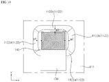
FIGS. 9 and10 , theseating portion 1121 may be generally rectangular. In this case, theinclined portion 1122 may include first to fourthinclined portions seating portion 1121. Here, the firstinclined portion 1122a may be disposed between one end and the other end of thesheet 130. That is, thesheet 130 having one end adjacent to the lower end of thefirst plate 110 may extend upward and may pass through the firstinclined portion 1122a to be seated on theseating portion 1121. - The
sheet 130 may be spaced apart from the second to fourthinclined portions inclined portion 1122, except for the firstinclined portion 1122a disposed between the one end and the other end of thesheet 130. For example, a left side of thesheet 130 may be spaced apart from the secondinclined portion 1122b, disposed on the left of theseating portion 1121, by a predetermined gap g2. For example, an upper side of thesheet 130 may be spaced apart from the thirdinclined portion 1122c, disposed over theseating portion 1121, by a predetermined gap g3. For example, the right side of thesheet 130 may be spaced apart from the fourthinclined portion 1122d, disposed on the right of theseating portion 1121, by a predetermined gap g4. - That is, the
sheet 130 is placed on theseating portion 1121 without overlapping with the second to fourthinclined portions sheet 130, which increases in volume by absorbing the fluid FL, from narrowing the space S formed between the second to fourthinclined portions second body 121. - In addition, it should be understood that in order to secure the space S between the
seating portion 1121 and thesecond body 121 for the fluid FL to smoothly flow even when thesheet 130 increases in volume, a gap between thesecond body 121 and theseating portion 1121 is relatively greater than a gap between thesecond body 121 and theinclined portion 1122. - Accordingly, even when the
sheet 130 increases in volume by absorbing the fluid FL, the fluid FL evaporated from thesheet 130 may flow smoothly through the space S. Further, it is possible to prevent boiling noise which occurs when the evaporated fluid FL remains stagnant in theheat absorbing part 112. - A
mesh 40 may be disposed opposite to theseating portion 1121 with the sheet disposedtherebetween 130. Themesh 140 may have a plurality of pores formed therein. Themesh 140 may be coupled to thesheet 130. Themesh 130 may reduce noise occurring when bubbles of the fluid FL jetting through thesheet 130 burst. That is, the bubbles, generated when the fluid FL is evaporated from thesheet 130, may be reduced in size by the plurality of pores of themesh 140, such that the bubbles may burst without causing loud noise. - For example, the
mesh 140 is generally rectangular. For example, themesh 140 may include a metal material. For example, themesh 140 may include stainless steel which is excellent in corrosion resistance. - According to an aspect of the present disclosure, there is provided a display device including: a display panel; a module cover disposed at a rear of the display panel; a PCB coupled to the module cover and on which a plurality of elements are positioned; and a vapor chamber coupled to the PCB, and that contacts a contact element which is at least any one of the plurality of elements, wherein the vapor chamber includes: a first plate including a heat absorbing part that contacts the contact element; a second plate coupled to the first plate; and a fluid flowing through a space provided between the first plate and the second plate, wherein the first plate extends upward from the heat absorbing part while bypassing a protruding element so as not to overlap with the protruding element in a front-rear direction, the protruding element overlapping with the first plate in an up-down direction among the plurality of elements.
- In addition, according to another aspect of the present disclosure, the fluid may be evaporated by the heat in the heat absorbing part to flow upwardly, and may be condensed in an upper portion of the space to flow downwardly.
- In addition, according to another aspect of the present disclosure, the protruding element may include a plurality of protruding elements which are spaced apart from each other, wherein the first plate may bypass each of the plurality of protruding elements in a same direction.
- In addition, according to another aspect of the present disclosure, the first plate may be spaced apart from the plurality of elements at portions except for the heat absorbing part.
- In addition, according to another aspect of the present disclosure, the first plate may include a first body having the heat absorbing part formed therein, wherein the heat absorbing part may protrude from the first body toward the PCB.
- In addition, according to another aspect of the present disclosure, there is further included an adhesive disposed between the heat absorbing part and the contact element, and coupled to each of the heat absorbing part and the contact element.
- In addition, according to another aspect of the present disclosure, there is further included a bracket having one side coupled to the vapor chamber, and the other side coupled to the PCB.
- In addition, according to another aspect of the present disclosure, the other side of the bracket may have a hole formed therein, through which a fastening member fastened to the PCB passes, and may be spaced apart from the PCB.
- In addition, according to another aspect of the present disclosure, there are further included: a pipe which is inserted into a hole formed in the second plate, and through which the fluid provided to the space through the hole flows; and a cap coupled to the second plate and covering the pipe, wherein the cap may be elongated in the front-rear direction.
- In addition, according to another aspect of the present disclosure, an upper end of the vapor chamber may be adjacent to an upper end of the module cover.
- Certain embodiments or other embodiments of the invention described above are not mutually exclusive or distinct from each other. Any or all elements of the embodiments of the invention described above may be combined or combined with each other in configuration or function.
- For example, a configuration "A" described in one embodiment of the invention and the drawings and a configuration "B" described in another embodiment of the invention and the drawings may be combined with each other. Namely, although the combination between the configurations is not directly described, the combination is possible except in the case where it is described that the combination is impossible.
- Although embodiments have been described with reference to a number of illustrative embodiments thereof, it should be understood that numerous other modifications and embodiments can be devised by those skilled in the art that will fall within the scope of the principles of this disclosure. More particularly, various variations and modifications are possible in the component parts and/or arrangements of the subject combination arrangement within the scope of the disclosure, the drawings and the appended claims. In addition to variations and modifications in the component parts and/or arrangements, alternative uses will also be apparent to those skilled in the art.
Claims (10)
- A display device comprising:a display panel;a module cover disposed at a rear of the display panel;a PCB coupled to the module cover and on which a plurality of elements are positioned; anda vapor chamber coupled to the PCB, and that contacts a contact element which is at least any one of the plurality of elements,wherein the vapor chamber comprises:a first plate including a heat absorbing part that contacts the contact element;a second plate coupled to the first plate; anda fluid flowing through a space provided between the first plate and the second plate,wherein the first plate extends upward from the heat absorbing part while bypassing a protruding element so as not to overlap with the protruding element in a front-rear direction, the protruding element overlapping with the first plate in an up-down direction among the plurality of elements.
- The display device of claim 1, wherein the fluid is evaporated by the heat in the heat absorbing part to flow upwardly, and is condensed in an upper portion of the space to flow downwardly.
- The display device of claim 1, wherein the protruding element comprises a plurality of protruding elements which are spaced apart from each other,
wherein the first plate bypasses each of the plurality of protruding elements in a same direction. - The display device of claim 1, wherein the first plate is spaced apart from the plurality of elements at portions except for the heat absorbing part.
- The display device of claim 4, wherein the first plate comprises a first body having the heat absorbing part formed therein,
wherein the heat absorbing part protrudes from the first body toward the PCB. - The display device of claim 5, further comprising an adhesive disposed between the heat absorbing part and the contact element, and coupled to each of the heat absorbing part and the contact element.
- The display device of claim 5, further comprising a bracket having one side coupled to the vapor chamber, and the other side coupled to the PCB.
- The display device of claim 7, wherein the other side of the bracket has a hole formed therein, through which a fastening member fastened to the PCB passes, and is spaced apart from the PCB.
- The display device of claim 1, further comprising:a pipe which is inserted into a hole formed in the second plate, and through which the fluid provided to the space through the hole flows; anda cap coupled to the second plate and covering the pipe,wherein the cap is elongated in the front-rear direction.
- The display device of claim 1, wherein an upper end of the vapor chamber is adjacent to an upper end of the module cover.
Applications Claiming Priority (1)
| Application Number | Priority Date | Filing Date | Title |
|---|---|---|---|
| PCT/KR2020/000201 WO2021141148A1 (en) | 2020-01-06 | 2020-01-06 | Display device |
Publications (3)
| Publication Number | Publication Date |
|---|---|
| EP4089664A1 true EP4089664A1 (en) | 2022-11-16 |
| EP4089664A4 EP4089664A4 (en) | 2023-11-08 |
| EP4089664B1 EP4089664B1 (en) | 2025-08-27 |
Family
ID=76788048
Family Applications (1)
| Application Number | Title | Priority Date | Filing Date |
|---|---|---|---|
| EP20911743.1A Active EP4089664B1 (en) | 2020-01-06 | 2020-01-06 | Display device |
Country Status (4)
| Country | Link |
|---|---|
| US (1) | US20230032004A1 (en) |
| EP (1) | EP4089664B1 (en) |
| KR (1) | KR102751012B1 (en) |
| WO (1) | WO2021141148A1 (en) |
Families Citing this family (2)
| Publication number | Priority date | Publication date | Assignee | Title |
|---|---|---|---|---|
| CN113891620B (en) * | 2021-09-27 | 2023-05-23 | 联想(北京)有限公司 | Heat abstractor and electronic equipment |
| KR102718736B1 (en) * | 2022-07-07 | 2024-10-16 | 엘지전자 주식회사 | Display device |
Family Cites Families (21)
| Publication number | Priority date | Publication date | Assignee | Title |
|---|---|---|---|---|
| US8172097B2 (en) * | 2005-11-10 | 2012-05-08 | Daktronics, Inc. | LED display module |
| US20090040726A1 (en) * | 2007-08-09 | 2009-02-12 | Paul Hoffman | Vapor chamber structure and method for manufacturing the same |
| KR101056323B1 (en) * | 2009-09-15 | 2011-08-11 | 삼성모바일디스플레이주식회사 | Flat Panel Display |
| KR101057885B1 (en) * | 2009-12-18 | 2011-08-19 | 이상갑 | Heat dissipation device for heating element and manufacturing method thereof |
| KR20120103261A (en) * | 2011-03-10 | 2012-09-19 | 삼성전자주식회사 | Liquid crystal display apparatus |
| US8857502B2 (en) * | 2011-07-26 | 2014-10-14 | Kunshan Jue-Chung Electronics Co., Ltd. | Vapor chamber having heated protrusion |
| US20140076995A1 (en) * | 2012-09-14 | 2014-03-20 | Chin-Wen Wang | Vapor chamber and method of manufacturing the same |
| KR101996653B1 (en) * | 2012-10-30 | 2019-07-05 | 삼성디스플레이 주식회사 | Flat panel display device |
| JP2014214985A (en) * | 2013-04-26 | 2014-11-17 | 富士通株式会社 | Evaporator, cooler, and electronic apparatus |
| US20150026981A1 (en) * | 2013-07-24 | 2015-01-29 | Asia Vital Components Co., Ltd. | Manufacturing mehtod of vapor chamber structure |
| KR20150091905A (en) * | 2014-02-04 | 2015-08-12 | 엘지전자 주식회사 | Vapor chamber |
| KR102099255B1 (en) * | 2014-05-07 | 2020-04-10 | 삼성전자주식회사 | Heat-dissipating apparatus and electronic device having thereof |
| US11397057B2 (en) * | 2014-09-26 | 2022-07-26 | Asia Vital Components Co., Ltd. | Vapor chamber structure |
| KR102317133B1 (en) * | 2015-01-21 | 2021-10-22 | 엘지디스플레이 주식회사 | Organic light emitting display device and display apparatus having the same |
| US20170038154A1 (en) * | 2015-08-06 | 2017-02-09 | Chaun-Choung Technology Corp. | Vapor chamber structure having stretchable heated part |
| US10561041B2 (en) * | 2017-10-18 | 2020-02-11 | Pimems, Inc. | Titanium thermal module |
| KR102487229B1 (en) * | 2017-11-24 | 2023-01-11 | 삼성전자 주식회사 | Electronic device comprising heat dissipation structure |
| US20190343021A1 (en) * | 2018-05-07 | 2019-11-07 | Asia Vital Components Co., Ltd. | Heat dissipation unit connection reinforcement structure |
| JP7279151B2 (en) * | 2019-03-19 | 2023-05-22 | 株式会社ソニー・インタラクティブエンタテインメント | head mounted display |
| US20220151113A1 (en) * | 2019-03-28 | 2022-05-12 | Nec Corporation | Electronic device |
| KR20210001152A (en) * | 2019-06-27 | 2021-01-06 | 삼성전자주식회사 | Electronic device including heat dissipating structure |
-
2020
- 2020-01-06 KR KR1020227012089A patent/KR102751012B1/en active Active
- 2020-01-06 WO PCT/KR2020/000201 patent/WO2021141148A1/en not_active Ceased
- 2020-01-06 US US17/758,444 patent/US20230032004A1/en not_active Abandoned
- 2020-01-06 EP EP20911743.1A patent/EP4089664B1/en active Active
Also Published As
| Publication number | Publication date |
|---|---|
| KR20220062078A (en) | 2022-05-13 |
| WO2021141148A1 (en) | 2021-07-15 |
| KR102751012B1 (en) | 2025-01-06 |
| EP4089664B1 (en) | 2025-08-27 |
| EP4089664A4 (en) | 2023-11-08 |
| US20230032004A1 (en) | 2023-02-02 |
Similar Documents
| Publication | Publication Date | Title |
|---|---|---|
| CN113644089B (en) | Display device | |
| JP4482473B2 (en) | Liquid crystal display | |
| US20100079942A1 (en) | Video display apparatus | |
| JP2010085782A (en) | Image display device | |
| JPWO2008078587A1 (en) | Light emitting device, display device, and solid light emitting element substrate | |
| EP4089664A1 (en) | Display device | |
| KR102304816B1 (en) | Display device | |
| CN103531102A (en) | Display apparatus | |
| KR102899395B1 (en) | display device | |
| KR102292254B1 (en) | Display device | |
| JP2015012063A (en) | Video output device | |
| JP5188245B2 (en) | Display device | |
| US8770805B2 (en) | Backlight module for liquid crystal display and liquid crystal display | |
| JPH1096898A (en) | Liquid crystal display device | |
| JPH07212689A (en) | Plasma display device | |
| KR102454071B1 (en) | Display device | |
| JPH1124072A (en) | Liquid crystal display | |
| JP2009163152A (en) | Display device | |
| JPH10207381A (en) | Display heat dissipation device | |
| KR102718736B1 (en) | Display device | |
| CN215220133U (en) | An LED display with eye protection function | |
| JP2006227427A (en) | Display device | |
| JPH11327449A (en) | Plasma display device | |
| TWI916887B (en) | Electronic device | |
| CN217767117U (en) | Display assembly and on-vehicle display device of effective heat dissipation, reduction surface temperature rise |
Legal Events
| Date | Code | Title | Description |
|---|---|---|---|
| STAA | Information on the status of an ep patent application or granted ep patent |
Free format text: STATUS: THE INTERNATIONAL PUBLICATION HAS BEEN MADE |
|
| PUAI | Public reference made under article 153(3) epc to a published international application that has entered the european phase |
Free format text: ORIGINAL CODE: 0009012 |
|
| STAA | Information on the status of an ep patent application or granted ep patent |
Free format text: STATUS: REQUEST FOR EXAMINATION WAS MADE |
|
| 17P | Request for examination filed |
Effective date: 20220803 |
|
| AK | Designated contracting states |
Kind code of ref document: A1 Designated state(s): AL AT BE BG CH CY CZ DE DK EE ES FI FR GB GR HR HU IE IS IT LI LT LU LV MC MK MT NL NO PL PT RO RS SE SI SK SM TR |
|
| DAV | Request for validation of the european patent (deleted) | ||
| DAX | Request for extension of the european patent (deleted) | ||
| REG | Reference to a national code |
Ref country code: DE Ref legal event code: R079 Free format text: PREVIOUS MAIN CLASS: G09F0009330000 Ipc: H05K0007200000 Ref document number: 602020057746 Country of ref document: DE |
|
| A4 | Supplementary search report drawn up and despatched |
Effective date: 20231009 |
|
| RIC1 | Information provided on ipc code assigned before grant |
Ipc: H10K 50/84 20230101ALI20231002BHEP Ipc: H05K 7/20 20060101AFI20231002BHEP |
|
| GRAP | Despatch of communication of intention to grant a patent |
Free format text: ORIGINAL CODE: EPIDOSNIGR1 |
|
| STAA | Information on the status of an ep patent application or granted ep patent |
Free format text: STATUS: GRANT OF PATENT IS INTENDED |
|
| INTG | Intention to grant announced |
Effective date: 20250331 |
|
| GRAS | Grant fee paid |
Free format text: ORIGINAL CODE: EPIDOSNIGR3 |
|
| GRAA | (expected) grant |
Free format text: ORIGINAL CODE: 0009210 |
|
| STAA | Information on the status of an ep patent application or granted ep patent |
Free format text: STATUS: THE PATENT HAS BEEN GRANTED |
|
| AK | Designated contracting states |
Kind code of ref document: B1 Designated state(s): AL AT BE BG CH CY CZ DE DK EE ES FI FR GB GR HR HU IE IS IT LI LT LU LV MC MK MT NL NO PL PT RO RS SE SI SK SM TR |
|
| REG | Reference to a national code |
Ref country code: CH Ref legal event code: EP |
|
| REG | Reference to a national code |
Ref country code: DE Ref legal event code: R096 Ref document number: 602020057746 Country of ref document: DE |
|
| REG | Reference to a national code |
Ref country code: IE Ref legal event code: FG4D |
|
| REG | Reference to a national code |
Ref country code: NL Ref legal event code: MP Effective date: 20250827 |
|
| PG25 | Lapsed in a contracting state [announced via postgrant information from national office to epo] |
Ref country code: IS Free format text: LAPSE BECAUSE OF FAILURE TO SUBMIT A TRANSLATION OF THE DESCRIPTION OR TO PAY THE FEE WITHIN THE PRESCRIBED TIME-LIMIT Effective date: 20251227 |
|
| PGFP | Annual fee paid to national office [announced via postgrant information from national office to epo] |
Ref country code: GB Payment date: 20251208 Year of fee payment: 7 |
|
| PG25 | Lapsed in a contracting state [announced via postgrant information from national office to epo] |
Ref country code: NO Free format text: LAPSE BECAUSE OF FAILURE TO SUBMIT A TRANSLATION OF THE DESCRIPTION OR TO PAY THE FEE WITHIN THE PRESCRIBED TIME-LIMIT Effective date: 20251127 |
|
| REG | Reference to a national code |
Ref country code: LT Ref legal event code: MG9D |
|
| PG25 | Lapsed in a contracting state [announced via postgrant information from national office to epo] |
Ref country code: PT Free format text: LAPSE BECAUSE OF FAILURE TO SUBMIT A TRANSLATION OF THE DESCRIPTION OR TO PAY THE FEE WITHIN THE PRESCRIBED TIME-LIMIT Effective date: 20251229 |
|
| PG25 | Lapsed in a contracting state [announced via postgrant information from national office to epo] |
Ref country code: FI Free format text: LAPSE BECAUSE OF FAILURE TO SUBMIT A TRANSLATION OF THE DESCRIPTION OR TO PAY THE FEE WITHIN THE PRESCRIBED TIME-LIMIT Effective date: 20250827 |
|
| PG25 | Lapsed in a contracting state [announced via postgrant information from national office to epo] |
Ref country code: NL Free format text: LAPSE BECAUSE OF FAILURE TO SUBMIT A TRANSLATION OF THE DESCRIPTION OR TO PAY THE FEE WITHIN THE PRESCRIBED TIME-LIMIT Effective date: 20250827 Ref country code: HR Free format text: LAPSE BECAUSE OF FAILURE TO SUBMIT A TRANSLATION OF THE DESCRIPTION OR TO PAY THE FEE WITHIN THE PRESCRIBED TIME-LIMIT Effective date: 20250827 |
|
| PGFP | Annual fee paid to national office [announced via postgrant information from national office to epo] |
Ref country code: FR Payment date: 20251209 Year of fee payment: 7 |
|
| PG25 | Lapsed in a contracting state [announced via postgrant information from national office to epo] |
Ref country code: GR Free format text: LAPSE BECAUSE OF FAILURE TO SUBMIT A TRANSLATION OF THE DESCRIPTION OR TO PAY THE FEE WITHIN THE PRESCRIBED TIME-LIMIT Effective date: 20251128 |
|
| PG25 | Lapsed in a contracting state [announced via postgrant information from national office to epo] |
Ref country code: SE Free format text: LAPSE BECAUSE OF FAILURE TO SUBMIT A TRANSLATION OF THE DESCRIPTION OR TO PAY THE FEE WITHIN THE PRESCRIBED TIME-LIMIT Effective date: 20250827 |
|
| PG25 | Lapsed in a contracting state [announced via postgrant information from national office to epo] |
Ref country code: LV Free format text: LAPSE BECAUSE OF FAILURE TO SUBMIT A TRANSLATION OF THE DESCRIPTION OR TO PAY THE FEE WITHIN THE PRESCRIBED TIME-LIMIT Effective date: 20250827 |
|
| PG25 | Lapsed in a contracting state [announced via postgrant information from national office to epo] |
Ref country code: BG Free format text: LAPSE BECAUSE OF FAILURE TO SUBMIT A TRANSLATION OF THE DESCRIPTION OR TO PAY THE FEE WITHIN THE PRESCRIBED TIME-LIMIT Effective date: 20250827 Ref country code: PL Free format text: LAPSE BECAUSE OF FAILURE TO SUBMIT A TRANSLATION OF THE DESCRIPTION OR TO PAY THE FEE WITHIN THE PRESCRIBED TIME-LIMIT Effective date: 20250827 |
|
| PG25 | Lapsed in a contracting state [announced via postgrant information from national office to epo] |
Ref country code: RS Free format text: LAPSE BECAUSE OF FAILURE TO SUBMIT A TRANSLATION OF THE DESCRIPTION OR TO PAY THE FEE WITHIN THE PRESCRIBED TIME-LIMIT Effective date: 20251127 |
|
| PG25 | Lapsed in a contracting state [announced via postgrant information from national office to epo] |
Ref country code: ES Free format text: LAPSE BECAUSE OF FAILURE TO SUBMIT A TRANSLATION OF THE DESCRIPTION OR TO PAY THE FEE WITHIN THE PRESCRIBED TIME-LIMIT Effective date: 20250827 |
|
| REG | Reference to a national code |
Ref country code: AT Ref legal event code: MK05 Ref document number: 1831708 Country of ref document: AT Kind code of ref document: T Effective date: 20250827 |
|
| PG25 | Lapsed in a contracting state [announced via postgrant information from national office to epo] |
Ref country code: SM Free format text: LAPSE BECAUSE OF FAILURE TO SUBMIT A TRANSLATION OF THE DESCRIPTION OR TO PAY THE FEE WITHIN THE PRESCRIBED TIME-LIMIT Effective date: 20250827 |
|
| PG25 | Lapsed in a contracting state [announced via postgrant information from national office to epo] |
Ref country code: DK Free format text: LAPSE BECAUSE OF FAILURE TO SUBMIT A TRANSLATION OF THE DESCRIPTION OR TO PAY THE FEE WITHIN THE PRESCRIBED TIME-LIMIT Effective date: 20250827 |
|
| PGFP | Annual fee paid to national office [announced via postgrant information from national office to epo] |
Ref country code: DE Payment date: 20251208 Year of fee payment: 7 |
|
| PG25 | Lapsed in a contracting state [announced via postgrant information from national office to epo] |
Ref country code: AT Free format text: LAPSE BECAUSE OF FAILURE TO SUBMIT A TRANSLATION OF THE DESCRIPTION OR TO PAY THE FEE WITHIN THE PRESCRIBED TIME-LIMIT Effective date: 20250827 |
|
| PG25 | Lapsed in a contracting state [announced via postgrant information from national office to epo] |
Ref country code: IT Free format text: LAPSE BECAUSE OF FAILURE TO SUBMIT A TRANSLATION OF THE DESCRIPTION OR TO PAY THE FEE WITHIN THE PRESCRIBED TIME-LIMIT Effective date: 20250827 |
|
| PG25 | Lapsed in a contracting state [announced via postgrant information from national office to epo] |
Ref country code: CZ Free format text: LAPSE BECAUSE OF FAILURE TO SUBMIT A TRANSLATION OF THE DESCRIPTION OR TO PAY THE FEE WITHIN THE PRESCRIBED TIME-LIMIT Effective date: 20250827 |
|
| PG25 | Lapsed in a contracting state [announced via postgrant information from national office to epo] |
Ref country code: EE Free format text: LAPSE BECAUSE OF FAILURE TO SUBMIT A TRANSLATION OF THE DESCRIPTION OR TO PAY THE FEE WITHIN THE PRESCRIBED TIME-LIMIT Effective date: 20250827 Ref country code: SK Free format text: LAPSE BECAUSE OF FAILURE TO SUBMIT A TRANSLATION OF THE DESCRIPTION OR TO PAY THE FEE WITHIN THE PRESCRIBED TIME-LIMIT Effective date: 20250827 |