EP4087232B1 - Elektronische vorrichtung und verfahren für automatische fokussierung - Google Patents
Elektronische vorrichtung und verfahren für automatische fokussierung Download PDFInfo
- Publication number
- EP4087232B1 EP4087232B1 EP21751143.5A EP21751143A EP4087232B1 EP 4087232 B1 EP4087232 B1 EP 4087232B1 EP 21751143 A EP21751143 A EP 21751143A EP 4087232 B1 EP4087232 B1 EP 4087232B1
- Authority
- EP
- European Patent Office
- Prior art keywords
- data
- paf
- electronic device
- calculation
- processing unit
- Prior art date
- Legal status (The legal status is an assumption and is not a legal conclusion. Google has not performed a legal analysis and makes no representation as to the accuracy of the status listed.)
- Active
Links
Images


Classifications
-
- H—ELECTRICITY
- H04—ELECTRIC COMMUNICATION TECHNIQUE
- H04N—PICTORIAL COMMUNICATION, e.g. TELEVISION
- H04N23/00—Cameras or camera modules comprising electronic image sensors; Control thereof
- H04N23/60—Control of cameras or camera modules
- H04N23/67—Focus control based on electronic image sensor signals
- H04N23/672—Focus control based on electronic image sensor signals based on the phase difference signals
-
- H—ELECTRICITY
- H04—ELECTRIC COMMUNICATION TECHNIQUE
- H04N—PICTORIAL COMMUNICATION, e.g. TELEVISION
- H04N25/00—Circuitry of solid-state image sensors [SSIS]; Control thereof
- H04N25/70—SSIS architectures; Circuits associated therewith
- H04N25/703—SSIS architectures incorporating pixels for producing signals other than image signals
- H04N25/704—Pixels specially adapted for focusing, e.g. phase difference pixel sets
-
- H—ELECTRICITY
- H10—SEMICONDUCTOR DEVICES; ELECTRIC SOLID-STATE DEVICES NOT OTHERWISE PROVIDED FOR
- H10F—INORGANIC SEMICONDUCTOR DEVICES SENSITIVE TO INFRARED RADIATION, LIGHT, ELECTROMAGNETIC RADIATION OF SHORTER WAVELENGTH OR CORPUSCULAR RADIATION
- H10F39/00—Integrated devices, or assemblies of multiple devices, comprising at least one element covered by group H10F30/00, e.g. radiation detectors comprising photodiode arrays
- H10F39/10—Integrated devices
- H10F39/12—Image sensors
- H10F39/18—Complementary metal-oxide-semiconductor [CMOS] image sensors; Photodiode array image sensors
- H10F39/182—Colour image sensors
-
- H—ELECTRICITY
- H04—ELECTRIC COMMUNICATION TECHNIQUE
- H04N—PICTORIAL COMMUNICATION, e.g. TELEVISION
- H04N25/00—Circuitry of solid-state image sensors [SSIS]; Control thereof
- H04N25/10—Circuitry of solid-state image sensors [SSIS]; Control thereof for transforming different wavelengths into image signals
- H04N25/11—Arrangement of colour filter arrays [CFA]; Filter mosaics
-
- H—ELECTRICITY
- H10—SEMICONDUCTOR DEVICES; ELECTRIC SOLID-STATE DEVICES NOT OTHERWISE PROVIDED FOR
- H10F—INORGANIC SEMICONDUCTOR DEVICES SENSITIVE TO INFRARED RADIATION, LIGHT, ELECTROMAGNETIC RADIATION OF SHORTER WAVELENGTH OR CORPUSCULAR RADIATION
- H10F39/00—Integrated devices, or assemblies of multiple devices, comprising at least one element covered by group H10F30/00, e.g. radiation detectors comprising photodiode arrays
- H10F39/80—Constructional details of image sensors
- H10F39/806—Optical elements or arrangements associated with the image sensors
- H10F39/8063—Microlenses
Definitions
- Various embodiments of the disclosure relate to an electronic device for capturing an image and a method for performing auto focus (AF).
- AF auto focus
- the electronic device may recognize an object to perform auto focus (AF).
- AF auto focus
- a phase auto focus (PAF) scheme for detecting a phase difference between two pixels adjacent to each other and determining a focus is used as a method for performing auto focus (AF).
- the PAF scheme may be compared with a continuous AF scheme for measuring a focus depending on a change in planar frequency characteristics of an image to obtain more accurate and fast result in determining directionality of the focus.
- An image sensor of an electronic device may perform AF by detecting a phase difference between 2 PDs arranged in a horizontal direction.
- 2 PDs separated horizontally may share one microlens and may be separated by a pixel wall. Lights incident through the microlens may be differently refracted along a path to be separated from each other. Because the image is formed horizontally by the same lens, when the focus is matched and there is a subject in an arrangement direction of pixels, characteristics and level values of pixels located horizontally may be varied. In this case, an edge separated in a vertical direction causes a problem incapable of detecting an ideal value irrespective of whether the focus is matched.
- an AF detection circuit When using a 4PD image sensor including 4 (2x2) PDs separated in a horizontal direction and a vertical direction, an AF detection circuit performs calculation in the horizontal direction and calculation in the vertical direction at the same time, thus needing relatively many buffers therein to check a correlation between pixels adjacent to each other. Furthermore, the calculation process becomes complicated and there may occur a problem due to an increase in power consumption or cost.
- Various embodiments of the disclosure may simultaneously or sequentially process AF data in a plurality of directions using data obtained by a 4PD image sensor.
- an electronic device may include an image sensor including a plurality of pixels, an AF processing unit that performs calculation for performing auto focus based on a phase difference, a memory, and a controller that delivers data obtained by the image sensor to the AF processing unit or the memory.
- Each pixel included in the plurality of pixels may include a plurality of photo diodes and a microlens that covers the plurality of photo diodes.
- the controller may provide the AF processing unit with at least one of first AF data of photo diodes arranged in a first direction among the plurality of photo diodes or second AF data of photo diodes arranged in a second direction among the plurality of photo diodes.
- the AF processing unit may perform first phase auto focus (PAF) calculation based on the first AF data or may perform second PAF calculation based on the second AF data.
- PAF phase auto focus
- the electronic device may simultaneously or sequentially process AF data in a plurality of directions using data obtained by an image sensor.
- the electronic device may detect directionality of an edge and may reorder AF data in an edge direction, thus simplifying calculation of an AF detection circuit.
- the electronic device may reduce a calculation time and may enhance AF accuracy by means of rotation or reordering of the AF data of the image sensor.
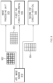
- FIG. 1 illustrates an electronic device capable of capturing an image according to an embodiment.
- the camera module 110 may include, for example, a lens assembly including one or more lens and an image sensor. Each pixel of the image sensor may include a plurality of photo diodes.
- the electronic device 100 may generate phase difference data (or depth data) by optical path differences generated by the plurality of photo diodes (hereinafter, PDs) which share a microlens.
- PDs photo diodes
- the electronic device 100 may adjust a focus on an external object 150 by moving the one or more lenses included in the camera module 110, based on the generated phase difference data.
- the electronic device 100 may display a preview image focusing on the external object on the display 120.
- the camera module 110 is the front camera of the electronic device 100 in FIG. 1 , but not limited thereto.
- the camera module 110 may be disposed on at least one of a rear surface or a side surface of the electronic device 100.
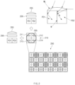
- FIG. 2 illustrates a configuration of an image sensor according to an embodiment.
- an image sensor 200 included in a camera module may include a plurality of pixels. It is illustratively shown that the image sensor 200 outputs a Bayer-patterned image based on a signal generated by a 4PD image sensor in FIG. 2 , but not limited thereto.
- one 210 of a plurality of pixels may include a microlens 205, a color filter 206, a first PD (or a first sub-pixel) (PD1) 211, a second PD (or a second sub-pixel) (PD2) 212, a third PD (or a third sub-pixel) (PD3) 213, and a fourth PD (or a fourth sub-pixel) (PD4) 214.
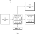
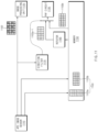
- the controller 420 may detect directionality from the AF data of the image sensor 410 for accurate and simple AF calculation with respect to horizontal and vertical or more directions and may reorder data in a dominant direction, such that the AF processing unit 450 performs AF calculation.
- the controller 420 may convert and deliver the image data or the AF data, received from the image sensor 410, to the memory 430, the image processing unit 440, or the AF processing unit 450 or may deliver the image data or the AF data to the memory 430, the image processing unit 440, or the AF processing unit 450 without a separate conversion task.
- the controller 420 may include a direction filter 421 or a rotator 422.
- the direction filter 421 may be used to determine a dominant direction among edge directions of an object.
- the rotator 422 may change the direction of the AF data to change the AF data in the form of data capable of being easily processed by the AF processing unit 450.
- the storage unit 430 may store the AF data (or the converted AF data).
- the storage unit 430 may be a DRAM.
- the stored AF data may be delivered to the AF processing unit 450 depending on directionality of an edge.
- the PAF circuit 451 may perform PAF calculation using AF data extracted from pixels (e.g., the first PD and the second PD or the third PD and the fourth PD) separated horizontally or may perform PAF calculation using AF data extracted from pixels (e.g., the first PD and the third PD or the second PD and the fourth PD) separated vertically.
- AF data extracted from pixels e.g., the first PD and the second PD or the third PD and the fourth PD
- AF circuit 451 may perform PAF calculation using AF data extracted from pixels (e.g., the first PD and the second PD or the third PD and the fourth PD) separated horizontally or may perform PAF calculation using AF data extracted from pixels (e.g., the first PD and the third PD or the second PD and the fourth PD) separated vertically.
- 2PD PAF circuit but not limited thereto.
- the camera module 400 may include a plurality of PAF circuits respectively corresponding to a plurality of edge directions capable of being detected by the image sensor 200.
- a plurality of PAF circuits respectively corresponding to a plurality of edge directions capable of being detected by the image sensor 200.
- two PAF circuits may be included.
- eight PAF circuits may be included.
- the camera module 400 may perform PAF calculation for the plurality of edge directions using one PAF circuit. For example, in case of the edge detection in the vertical/horizontal direction, PAF calculation of the edge in the horizontal direction may be primarily performed and PAF calculation of the edge in the vertical direction may be secondarily performed.
- the camera module 400 may determine a dominant direction among directions of edges using one PAF circuit, perform PAF for one dominant direction, and may fail to, or subsidiarily, proceed with PAF for other directions.
- controller 420, the image processing unit 440, or the AF processing unit 450 may be components (e.g., chips) separated in hardware.
- controller 420, the image processing unit 440, or the AF processing unit 450 may be operations separated in software in the same calculation element.
- FIG. 5 is an output timing diagram of image data and AF data according to various embodiments.
- the image sensor 410 may output image data (e.g., a Bayer signal) 510.
- image data e.g., a Bayer signal
- the image sensor 410 may output AF data 520 output at a longer time interval than the image data (e.g., the Bayer signal) 510, together with the image data (e.g., the Bayer signal) 510.
- the image sensor 410 may process AF data in a direction to obtain AF from the image data (e.g., the Bayer signal) 510 and may output the AF data 520 with smaller resolution than the image data (e.g., the Bayer signal) 510 by means of binning or the like.
- the image data e.g., the Bayer signal
- the image sensor 410 may process AF data in a direction to obtain AF from the image data (e.g., the Bayer signal) 510 and may output the AF data 520 with smaller resolution than the image data (e.g., the Bayer signal) 510 by means of binning or the like.
- the AF data AF_LR 521 in the horizontal direction and the AF data AF_TB 522 in the vertical direction are output at the same timing in FIG. 5 , but not limited thereto.
- the AF data AF_LR 521 in the horizontal direction and the AF data AF_TB 522 in the vertical direction are output at different timings.
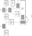
- a 4PD image sensor 610 may include four PDs in one pixel.
- the 4PD image sensor 610 may sequentially read out PDs included in each pixel to generate a multi-PD signal (or raw data) 601.
- An image generator 620 may integrate values of four PDs included in one pixel to generate image data 602.
- the image generator 620 may transmit the image data 602 to an image processing unit (e.g., an ISP) 625.
- an image processing unit e.g., an ISP
- a first AF data generator 630 may deliver AF data 603 in a first direction (e.g., a horizontal direction) in the multi-PD signal 601 to a first PAF circuit 635.
- a second AF data generator 640 may deliver AF data 604 in a second direction (e.g., a vertical direction) in the multi-PD signal 601 to a second PAF circuit 645.
- a second direction e.g., a vertical direction
- Each of the first PAF circuit 635 and the second PAF circuit 645 may perform PAF calculation for a different direction.
- the first PAF circuit 635 and the second PAF circuit 645 may perform AF calculation at the same time. As a result, quick and accurate AF may be performed.
- AF data for eight directions may be simultaneously and separately processed by eight PAF circuits.
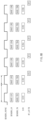
- FIG. 7A illustrates AF processing using one 2PD PAF circuit in a Bayer pattern according to various embodiments.
- the PAF circuit 735 may process the AF data 703 stored for each direction from the memory 750. According to an embodiment, the PAF circuit 735 may sequentially process the AF data 703 depending on a direction. For example, the PAF circuit 735 may primarily process the horizontal data 703b and may secondarily process the vertical data 703a.
- the rotator 760 may rotate and deliver signals in the other directions except for a first direction (e.g., a horizontal direction) to the PAF circuit 735.
- a first direction e.g., a horizontal direction
- the image sensor 710 may store AF data SAVE_LR and SAVE_TB at a specified time interval.
- a PAF circuit 735 may start PAF using the horizontal data SAVE_LR at a time when the storage of the horizontal data SAVE_LR is completed.
- PAF (AF_LR) for a horizontal direction may be completed at the same time that the storage of the horizontal data SAVE_LR is ended (or as a portion of the storage of the horizontal data SAVE_LR is delayed).
- the PAF circuit 735 may start PAF (AF_TB) using the stored vertical data SAVE_TB.
- PAF using the vertical data SAVE_TB may proceed in a state where the vertical data SAVE_TB in stored (a state where a timing signal SENSOR_VSYNC is low).
- AF data may be converted into a size smaller than image data to be output. It is possible to process PAF (AF_TB) within a relatively short time using the PAF (AF_LR) for the horizontal direction or the vertical data SAVE_TB. It may be possible to proceed with PAF (AF_TB), after the readout of all frames is completed because of having a different readout direction, using the vertical data SAVE_TB.
- the PAF circuit 735 may perform PAF calculation for a plurality of directions in the state where the timing signal SENSOR_VSYNC is low. For example, the PAF circuit 735 may perform PAF calculation for the plurality of directions in a vertical direction, a 45-degree direction, and a 125-degree direction in the state where the timing signal SENSOR_VSYNC is low.
- FIG. 8A illustrates AF processing using a direction filter in a Bayer pattern according to various embodiments.
- An image generator 820 may integrate values of four PDs included in one pixel to generate main image data 802.
- the image generator 820 may transmit the image data 802 to an image processing unit (e.g., an ISP) 825.
- an image processing unit e.g., an ISP
- the memory 850 may store the AF data 803.
- a storage unit 840 may be a memory buffer included in a camera module or a memory area formed independently of the camera module.
- a 4PD image sensor 910 may include four PDs in one pixel.
- the 4PD image sensor 910 may integrate values of four PDs included in one pixel to generate image data 902.
- the 4PD image sensor 910 may transmit the image data 902 to an image processing unit (e.g., an ISP) 925.
- an image processing unit e.g., an ISP
- the 4PD image sensor 910 may deliver first processing data 903 obtained by processing AF data in a first direction (e.g., a horizontal direction) to a first PAF circuit 935.
- a first direction e.g., a horizontal direction
- the 4PD image sensor 910 may deliver second processing data 904 obtained by processing AF data in a second direction (e.g., a vertical direction) to a second PAF circuit 945.
- a second direction e.g., a vertical direction
- Each of the first PAF circuit 935 and the second PAF circuit 945 may perform PAF calculation for a different direction.
- the first PAF circuit 935 and the second PAF circuit 945 may perform AF calculation at the same time. As a result, quick and accurate AF may be performed.
- AF data for eight directions may be simultaneously and separately processed by eight PAF circuits.
- FIG. 10 illustrates AF processing using one 2PD PAF circuit in a processing pattern according to various embodiments.
- the 4PD image sensor 1010 may store first processing data 903 obtained by processing AF data in a first direction (e.g., a horizontal direction) in a memory (e.g., a DRAM) 1050.
- first direction e.g., a horizontal direction
- a memory e.g., a DRAM
- vertical data 1003a and horizontal data 1003b may be stored.
- the memory 1050 may store the AF data 1003.
- a storage unit 1040 may be a memory buffer included in a camera module or a memory area formed independently of the camera module.
- a PAF circuit 1035 may process the AF data 1003 stored for each direction from the memory 1050. According to an embodiment, the PAF circuit 1035 may sequentially process the AF data 1003 depending on a direction. For example, the PAF circuit 1035 may primarily process the horizontal data 1003b and may secondarily process the vertical data 1003a.
- a rotator 1060 may rotate and deliver signals in the other directions except for the first direction (e.g., the horizontal direction) to the PAF circuit 1035.
- the vertical data 1003a may rotate at 90 degrees to be provided to the PAF circuit 1035 (1003a-1).
- the horizontal data 1003b and the converted vertical data 1003a-1 may have a data structure similar to each other, and the calculation process of the PAF circuit 1035 may be simplified.
- FIG. 11 illustrates AF processing using a direction filter in a processing pattern according to various embodiments.
- a 4PD image sensor 1110 may include 4 PDs in one pixel.
- the 4PD image sensor 1110 may integrate values of four PDs included in one pixel to generate image data 1102.
- the 4PD image sensor 1110 may transmit the image data 1102 to an image processing unit (e.g., an ISP) 1125.
- an image processing unit e.g., an ISP
- the 4PD image sensor 1110 may store first processing data 1103 obtained by processing AF data in a first direction (e.g., a horizontal direction) in a memory (e.g., a DRAM) 1150.
- first direction e.g., a horizontal direction
- a memory e.g., a DRAM
- vertical data 1103a and horizontal data 1103b may be stored.
- the memory 1150 may store the AF data 1103.
- a storage unit 1140 may be a memory buffer included in a camera module or a memory area formed independently of the camera module.
- the rotator 1160 may rotate and deliver signals in the other directions except for the first direction (e.g., the horizontal direction) to the PAF circuit 1135.
- the vertical data 1103a may rotate at 90 degrees to be provided to the PAF circuit 1135 (1103a-1).
- the horizontal data 1103b and the converted vertical data 1103a-1 may have a data structure similar to each other, and the calculation process of the PAF circuit 1135 may be simplified.
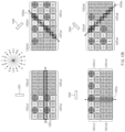
- a direction filter 1270 may compare detection values for the plurality of directions, in AF data using the multi-PD signal (or the raw data), to detect directionality (an edge direction) of an image. For example, when data of a first portion and a second portion are changed to a specified value or more by an external object among all pixels of the AF data, it may be determined that a boundary (edge) of the first portion and the second portion is formed.
- data of a first portion 1201a1 and a second portion 1201a2 of the 4PD image sensor 1210 may be changed to the specified value or more by a first object 1251.
- the direction filter 1270 may compare values of image data to detect an edge direction 1251a perpendicular to a boundary of the first portion 1201al and the second portion 1201a2 as a fifth direction (0 degree).
- data of a first portion 1201b1 and a second portion 1201b2 of the 4PD image sensor 1210 may be changed to the specified value or more by a second object 1252.
- the direction filter 1270 may compare values of image data to detect an edge direction 1252a perpendicular to a boundary of the first portion 1201b1 and the second portion 1201b2 as a third direction (45 degrees).
- data of a first portion 1201c1 and a second portion 1201c2 of the 4PD image sensor 1210 may be changed to the specified value or more by a third object 1253.
- the direction filter 1270 may compare values of image data to detect an edge direction 1253a perpendicular to a boundary of the first portion 1201c1 and the second portion 1201c2 as a first direction (90 degrees).
- data of a first portion 1201d1 and a second portion 1201d2 of the 4PD image sensor 1210 may be changed to the specified value or more by a fourth object 1254.
- the direction filter 1270 may compare values of image data to detect an edge direction 1254a perpendicular to a boundary of the first portion 1201d1 and the second portion 1201d2 as a seventh direction (135 degrees).
- a reordering unit 1280 may rotate or reorder AF data for each direction (or a direction where an edge is mainly disposed).
- the reordering unit 1280 may rotate or reorder AF data in an edge direction 1251a, 1252a, 1253a, or 1254a perpendicular to the boundary of the first portion 1201a1, 1201b1, 1201c1, or 1201d1 and the second portion 1201a2, 1201b2, 1201c2, or 1201d2.
- the PAF circuit 1235 may perform PAF calculation depending on directionality of an edge.
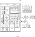
- the image stabilizer 1440 may move the image sensor 1430 or at least one lens included in the lens assembly 1410 in a particular direction, or control an operational attribute (e.g., adjust the read-out timing) of the image sensor 1430 in response to the movement of the camera module 1380 or the electronic device 1301 including the camera module 1380. This allows compensating for at least part of a negative effect (e.g., image blurring) by the movement on an image being captured.
- the image stabilizer 1440 may sense such a movement by the camera module 1380 or the electronic device 1301 using a gyro sensor (not shown) or an acceleration sensor (not shown) disposed inside or outside the camera module 1380.
- the AF controller may store the first AF data or the second AF data in the memory (e.g., the memory 430 of FIG. 4 , the memory 1330 of FIG. 13 , or the memory 1450 of FIG. 14 ).
- the AF controller e.g., the controller 420 of FIG. 4
- the AF processing unit may perform the first PAF calculation during a process where the first AF data and the second AF data are stored in the memory (e.g., the memory 430 of FIG. 4 , the memory 1330 of FIG. 13 , or the memory 1450 of FIG. 14 ) and may calculate the second PAF calculation after the process is ended.
- the memory e.g., the memory 430 of FIG. 4 , the memory 1330 of FIG. 13 , or the memory 1450 of FIG. 14
- the AF processing unit may perform the first PAF calculation while the first AF data and the second AF data are read out by means of the image sensor (e.g., the image sensor 200 of FIG. 2 or the image sensor 1430 of FIG. 14 ) and may perform the second PAF calculation after the readout is ended.
- the image sensor e.g., the image sensor 200 of FIG. 2 or the image sensor 1430 of FIG. 14
- the image sensor (e.g., the image sensor 200 of FIG. 2 or the image sensor 1430 of FIG. 14 ) may be formed such that one microlens covers four photo diodes.
- the AF processing unit (e.g., the AF processing unit 450 of FIG. 4 ) may compare measurement values of the two photo diodes to perform PAF calculation.
- An electronic device may include an image sensor (e.g., an image sensor 200 of FIG. 2 or an image sensor 1430 of FIG. 14 ) including a plurality of pixels, wherein each pixel included in the plurality of pixels includes a plurality of photo diodes and a microlens for covering the plurality of photo diodes, an AF processing unit (e.g., an AF processing unit 450 of FIG. 4 ) for performing calculation for performing auto focus based on a phase difference, a memory (e.g., a memory 430 of FIG. 4 , a memory 1330 of FIG. 13 , or a memory 1450 of FIG.
- an image sensor e.g., an image sensor 200 of FIG. 2 or an image sensor 1430 of FIG. 14
- an AF processing unit e.g., an AF processing unit 450 of FIG. 4
- a memory e.g., a memory 430 of FIG. 4 , a memory 1330 of FIG. 13 , or a memory 1450 of
- a controller e.g., a controller 420 of FIG. 4 for delivering data obtained by the image sensor (e.g., the image sensor 200 of FIG. 2 or the image sensor 1430 of FIG. 14 ) to the AF processing unit or the memory (e.g., the memory 430 of FIG. 4 , the memory 1330 of FIG. 13 , or the memory 1450 of FIG. 14 ).
- the controller e.g., the controller 420 of FIG. 4
- the controller may set priorities based on measurement values of photo diodes corresponding to a plurality of directions.
- the AF processing unit e.g., the AF processing unit 450 of FIG. 4
- the AF processing unit may include a plurality of PAF circuits respectively corresponding to the plurality of directions. Each of the plurality of PAF circuits may start PAF calculation at the same time.
- a method for performing auto focus (AF) performed in an electronic device may include obtaining image data by means of an image sensor (e.g., an image sensor 200 of FIG. 2 or an image sensor 1430 of FIG.
- the electronic device may include a first AF circuit and a second AF circuit.
- the performing of the first PAF calculation or the second PAF calculation may include performing the second phase auto focus (PAF) calculation by means of the second AF circuit, while performing the first phase auto focus (PAF) by means of the first AF circuit.
- PAF phase auto focus
- the electronic device may include one AF circuit.
- the performing of the first PAF calculation or the second PAF calculation may include performing the first phase auto focus (PAF) using the AF circuit and performing the second PAF calculation, when the first phase auto focus (PAF) calculation is ended.
- PAF phase auto focus
- the obtaining of the second AF data may include rotating the second AF data to correspond to the first direction.
- the performing of the first PAF calculation or the second PAF calculation may include selecting one of the first direction or the second direction by means of a direction filter of the electronic device (e.g., the electronic device 100 of FIG. 1 or the electronic device 1301 of FIG. 13 ) and performing PAF calculation for AF data corresponding to the selected direction.
- a direction filter of the electronic device e.g., the electronic device 100 of FIG. 1 or the electronic device 1301 of FIG. 13
- the method for performing the AF may further include storing the first AF data or the second AF data in a memory (e.g., a memory 430 of FIG. 4 , a memory 1330 of FIG. 13 , or a memory 1450 of FIG. 14 ) of the electronic device (e.g., the electronic device 100 of FIG. 1 or the electronic device 1301 of FIG. 13 ).
- a memory e.g., a memory 430 of FIG. 4 , a memory 1330 of FIG. 13 , or a memory 1450 of FIG. 14
- the electronic device e.g., the electronic device 100 of FIG. 1 or the electronic device 1301 of FIG. 13 .
- the electronic device may be one of various types of electronic devices.
- the electronic devices may include, for example, a portable communication device (e.g., a smartphone), a computer device, a portable multimedia device, a portable medical device, a camera, a wearable device, or a home appliance. According to an embodiment of the disclosure, the electronic devices are not limited to those described above.
- each of such phrases as “A or B”, “at least one of A and B”, “at least one of A or B”, “A, B, or C”, “at least one of A, B, and C”, and “at least one of A, B, or C” may include any one of, or all possible combinations of the items enumerated together in a corresponding one of the phrases.
- such terms as “1st” and “2nd”, or “first” and “second” may be used to simply distinguish a corresponding component from another, and does not limit the components in other aspect (e.g., importance or order).
- an element e.g., a first element
- the element may be coupled with the other element directly (e.g., wiredly), wirelessly, or via a third element.
- module may include a unit implemented in hardware, software, or firmware, and may interchangeably be used with other terms, for example, “logic”, “logic block”, “part”, or “circuitry”.
- a module may be a single integral component, or a minimum unit or part thereof, adapted to perform one or more functions.
- the module may be implemented in a form of an application-specific integrated circuit (ASIC).
- ASIC application-specific integrated circuit
- Various embodiments as set forth herein may be implemented as software (e.g., the program 1340) including one or more instructions that are stored in a storage medium (e.g., internal memory 1336 or external memory 1338) that is readable by a machine (e.g., the electronic device 1301).
- a processor(e.g., the processor 1320) of the machine e.g., the electronic device 1301) may invoke at least one of the one or more instructions stored in the storage medium, and execute it, with or without using one or more other components under the control of the processor. This allows the machine to be operated to perform at least one function according to the at least one instruction invoked.
- the one or more instructions may include a code generated by a compiler or a code executable by an interpreter.
- the machine-readable storage medium may be provided in the form of a non-transitory storage medium.
- non-transitory simply means that the storage medium is a tangible device, and does not include a signal (e.g., an electromagnetic wave), but this term does not differentiate between where data is semi-permanently stored in the storage medium and where the data is temporarily stored in the storage medium.
- a method may be included and provided in a computer program product.
- the computer program product may be traded as a product between a seller and a buyer.
- the computer program product may be distributed in the form of a machine-readable storage medium (e.g., compact disc read only memory (CD-ROM)), or be distributed (e.g., downloaded or uploaded) online via an application store (e.g., PlayStore TM ), or between two user devices (e.g., smart phones) directly. If distributed online, at least part of the computer program product may be temporarily generated or at least temporarily stored in the machine-readable storage medium, such as memory of the manufacturer's server, a server of the application store, or a relay server.
- CD-ROM compact disc read only memory
- an application store e.g., PlayStore TM
- two user devices e.g., smart phones
- each component e.g., a module or a program of the above-described components may include a single entity or multiple entities.
- a plurality of components may be integrated into a single component.
- the integrated component may still perform one or more functions of each of the plurality of components in the same or similar manner as they are performed by a corresponding one of the plurality of components before the integration.
Landscapes
- Engineering & Computer Science (AREA)
- Multimedia (AREA)
- Signal Processing (AREA)
- Studio Devices (AREA)
- Transforming Light Signals Into Electric Signals (AREA)
Claims (13)
- Elektronische Vorrichtung, umfassend:einen Bildsensor, der eine Vielzahl von Pixeln beinhaltet;eine Autofokus-, AF-, Verarbeitungseinheit, die dazu konfiguriert ist, eine Berechnung zum Durchführen eines Autofokus basierend auf einer Phasendifferenz durchzuführen;einen Speicher; undmindestens einen Prozessor, der dazu konfiguriert ist, Daten, die durch den Bildsensor erhalten werden, an die AF-Verarbeitungseinheit oder den Speicher zu liefern,wobei jedes Pixel, das in der Vielzahl von Pixeln enthalten ist, eine Vielzahl von Fotodioden und eine Mikrolinse beinhaltet, die dazu konfiguriert ist, die Vielzahl von Fotodioden zu bedecken,wobei der zumindest eine Prozessor dazu konfiguriert ist, die AF-Verarbeitungseinheit mit ersten AF-Daten von Fotodioden zu versehen, die in einer ersten Richtung unter der Vielzahl von Fotodioden angeordnet sind,wobei der mindestens eine Prozessor dazu konfiguriert ist, die AF-Verarbeitungseinheit mit zweiten AF-Daten von Fotodioden zu versehen, die in einer zweiten Richtung unter der Vielzahl von Fotodioden angeordnet sind, indem die zweiten AF-Daten gedreht oder neu geordnet werden, um eine Datenstruktur in der ersten Richtung aufzuweisen, undwobei die AF-Verarbeitungseinheit eine Berechnung eines ersten Phasenautofokus, PAF, basierend auf den ersten AF-Daten durchführt und eine Berechnung eines zweiten PAF basierend auf den zweiten AF-Daten durchführt.
- Elektronische Vorrichtung nach Anspruch 1, wobei die AF-Verarbeitungseinheit eine erste AF-Schaltung und eine zweite AF-Schaltung beinhaltet, undwobei die zweite AF-Schaltung die Berechnung des zweiten Phasenautofokus,PAF, durchführt, während die erste AF-Schaltung die Berechnung des ersten Phasenautofokus, PAF, durchführt.
- Elektronische Vorrichtung nach Anspruch 1, wobei die AF-Verarbeitungseinheit eine AF-Schaltung beinhaltet, und
wobei die AF-Schaltung die Berechnung des ersten Phasenautofokus, PAF, durchführt und den zweiten PAF durchführt, wenn die Berechnung des ersten Phasenautofokus, PAF, beendet ist. - Elektronische Vorrichtung nach Anspruch 1, wobei die AF-Verarbeitungseinheit die erste Richtung mittels eines Richtungsfilters auswählt und eine Berechnung eines PAFs für AF-Daten, die der ausgewählten ersten Richtung entsprechen, durchführt.
- Elektronische Vorrichtung nach Anspruch 1, wobei der mindestens eine Prozessor dazu konfiguriert ist, die ersten AF-Daten oder die zweiten AF-Daten in dem Speicher zu speichern.
- Elektronische Vorrichtung nach Anspruch 1, wobei der mindestens eine Prozessor dazu konfiguriert ist, die AF-Verarbeitungseinheit mit den ersten AF-Daten oder den zweiten AF-Daten mit einem Bayer-Muster oder einem Verarbeitungsmuster zu versehen.
- Elektronische Vorrichtung nach Anspruch 1, wobei die AF-Verarbeitungseinheit die Berechnung des ersten PAFs während eines Prozesses durchführt, bei dem die ersten AF-Daten und die zweiten AF-Daten in dem Speicher gespeichert sind, und
die Berechnung des zweiten PAFs berechnet, nachdem de Prozess beendet ist. - Elektronische Vorrichtung nach Anspruch 1, wobei die AF-Verarbeitungseinheit die Berechnung des ersten PAFs durchführt, während die ersten AF-Daten und die zweiten AF-Daten mittels des Bildsensors ausgelesen werden, und die Berechnung des zweiten PAFs durchführt, nachdem das Auslesen beendet ist.
- Elektronische Vorrichtung nach Anspruch 1, wobei der Bildsensor so ausgebildet ist, dass eine Mikrolinse vier Fotodioden abdeckt, und
wobei die AF-Verarbeitungseinheit Messwerte der zwei Fotodioden vergleicht, um eine Berechnung eines PAFs durchzuführen. - Elektronische Vorrichtung nach Anspruch 1, wobei der mindestens eine Prozessor dazu konfiguriert ist, Prioritäten basierend auf Messwerten von Fotodioden festzulegen, die einer Vielzahl von Richtungen entsprechen, und
wobei die AF-Verarbeitungseinheit eine Berechnung eines PAFs basierend auf den Prioritäten durchführt. - Elektronische Vorrichtung nach Anspruch 10, wobei die AF-Verarbeitungseinheit eine Vielzahl von PAF-Schaltungen beinhaltet, die jeweils der Vielzahl von Richtungen entsprechen, und
wobei jede der Vielzahl von PAF-Schaltungen die Berechnung eines PAFs zur gleichen Zeit startet. - Elektronische Vorrichtung nach Anspruch 12, wobei die AF-Verarbeitungseinheit eine AF-Schaltung beinhaltet, und
wobei die AF-Verarbeitungseinheit eine Berechnung eines PAFs in den Prioritäten sequentiell durchführt. - Verfahren zum Durchführen eines Autofokus, AF, der in einer elektronischen Vorrichtung durchgeführt wird, wobei das Verfahren Folgendes umfasst:Erhalten von Bilddaten unter Verwendung eines Bildsensors, der eine Vielzahl von Pixeln beinhaltet;Erhalten von ersten AF-Daten von Fotodioden, die in einer ersten Richtung unter einer Vielzahl von Fotodioden angeordnet sind, die in jedem Pixel enthalten sind, das in der Vielzahl von Pixeln enthalten ist, basierend auf den Bilddaten;Erhalten von zweiten AF-Daten von Fotodioden, die in einer zweiten Richtung unter der Vielzahl von Fotodioden angeordnet sind, basierend auf den Bilddaten, wobei die zweiten AF-Daten gedreht oder neu geordnet werden, um eine Datenstruktur in der ersten Richtung aufzuweisen; undDurchführen einer Berechnung eines ersten Phasenautofokus, PAF, basierend auf den ersten AF-Daten und Durchführen einer Berechnung eines zweiten PAF basierend auf den zweiten AF-Daten.
Applications Claiming Priority (2)
| Application Number | Priority Date | Filing Date | Title |
|---|---|---|---|
| KR1020200013175A KR102902548B1 (ko) | 2020-02-04 | 2020-02-04 | 전자 장치 및 af 수행 방법 |
| PCT/KR2021/001496 WO2021158043A1 (ko) | 2020-02-04 | 2021-02-04 | 전자 장치 및 오토 포커스 수행 방법 |
Publications (3)
| Publication Number | Publication Date |
|---|---|
| EP4087232A1 EP4087232A1 (de) | 2022-11-09 |
| EP4087232A4 EP4087232A4 (de) | 2023-09-27 |
| EP4087232B1 true EP4087232B1 (de) | 2025-07-09 |
Family
ID=77200265
Family Applications (1)
| Application Number | Title | Priority Date | Filing Date |
|---|---|---|---|
| EP21751143.5A Active EP4087232B1 (de) | 2020-02-04 | 2021-02-04 | Elektronische vorrichtung und verfahren für automatische fokussierung |
Country Status (5)
| Country | Link |
|---|---|
| US (1) | US12348865B2 (de) |
| EP (1) | EP4087232B1 (de) |
| KR (1) | KR102902548B1 (de) |
| CN (1) | CN115066882B (de) |
| WO (1) | WO2021158043A1 (de) |
Families Citing this family (2)
| Publication number | Priority date | Publication date | Assignee | Title |
|---|---|---|---|---|
| WO2023140678A1 (ko) * | 2022-01-21 | 2023-07-27 | 삼성전자 주식회사 | 이미지 센서를 포함하는 전자 장치 및 그 동작 방법 |
| JP7781116B2 (ja) * | 2023-08-10 | 2025-12-05 | キヤノン株式会社 | 焦点検出装置及び方法、電子機器、プログラム及び記憶媒体 |
Family Cites Families (24)
| Publication number | Priority date | Publication date | Assignee | Title |
|---|---|---|---|---|
| JP5146295B2 (ja) | 2008-12-15 | 2013-02-20 | ソニー株式会社 | 撮像装置および合焦制御方法 |
| US11017250B2 (en) * | 2010-06-07 | 2021-05-25 | Affectiva, Inc. | Vehicle manipulation using convolutional image processing |
| JP5856376B2 (ja) * | 2011-01-27 | 2016-02-09 | キヤノン株式会社 | 撮像装置及びその制御方法 |
| US9177983B2 (en) * | 2012-01-23 | 2015-11-03 | Omnivision Technologies, Inc. | Image sensor with optical filters having alternating polarization for 3D imaging |
| KR102028124B1 (ko) | 2013-05-24 | 2019-10-02 | 삼성전자주식회사 | 위상차 초점검출 가능한 촬상소자 |
| KR102125561B1 (ko) * | 2013-12-03 | 2020-06-22 | 삼성전자주식회사 | 촬영 장치 및 이의 제어 방법 |
| JP6474737B2 (ja) * | 2014-02-03 | 2019-02-27 | オリンパス株式会社 | 固体撮像装置および撮像システム |
| JP5982601B2 (ja) | 2014-03-18 | 2016-08-31 | 富士フイルム株式会社 | 撮像装置及び合焦制御方法 |
| KR102261728B1 (ko) * | 2014-12-17 | 2021-06-08 | 엘지이노텍 주식회사 | 영상 획득 장치 및 이를 포함하는 휴대용 단말기 |
| CN107533210A (zh) * | 2015-01-14 | 2018-01-02 | 因维萨热技术公司 | 相位检测自动聚焦 |
| US9787889B2 (en) | 2015-02-12 | 2017-10-10 | Semiconductor Components Industries, Llc | Dynamic auto focus zones for auto focus pixel systems |
| US20180039156A1 (en) * | 2015-02-26 | 2018-02-08 | Lg Innotek Co., Ltd. | Camera Module and Auto-Focus Adjustment Method Using Same |
| KR102374112B1 (ko) * | 2015-07-15 | 2022-03-14 | 삼성전자주식회사 | 오토 포커싱 픽셀을 포함하는 이미지 센서, 및 이를 포함하는 이미지 처리 시스템 |
| US9807294B2 (en) * | 2015-08-05 | 2017-10-31 | Omnivision Technologies, Inc. | Image sensor with symmetric multi-pixel phase-difference detectors, and associated methods |
| US10015389B2 (en) * | 2016-09-22 | 2018-07-03 | Omnivision Technologies, Inc. | Image sensor with asymmetric-microlens phase-detection auto-focus (PDAF) detectors, associated PDAF imaging system, and associated method |
| CN107105141B (zh) | 2017-04-28 | 2019-06-28 | Oppo广东移动通信有限公司 | 图像传感器、图像处理方法、成像装置和移动终端 |
| US10387477B2 (en) * | 2017-05-30 | 2019-08-20 | Qualcomm Incorporated | Calibration for phase detection auto focus (PDAF) camera systems |
| US10440301B2 (en) * | 2017-09-08 | 2019-10-08 | Apple Inc. | Image capture device, pixel, and method providing improved phase detection auto-focus performance |
| KR20190042353A (ko) * | 2017-10-16 | 2019-04-24 | 엘지전자 주식회사 | 이동 단말기 및 그 제어 방법 |
| US10958825B2 (en) * | 2017-10-17 | 2021-03-23 | Canon Kabushiki Kaisha | Electronic apparatus and method for controlling the same |
| US10410374B2 (en) | 2017-12-28 | 2019-09-10 | Semiconductor Components Industries, Llc | Image sensors with calibrated phase detection pixels |
| KR102545173B1 (ko) * | 2018-03-09 | 2023-06-19 | 삼성전자주식회사 | 위상 검출 픽셀들을 포함하는 이미지 센서 및 이미지 촬상 장치 |
| JP2020012879A (ja) * | 2018-07-13 | 2020-01-23 | オリンパス株式会社 | 撮像素子、焦点検出装置、撮像方法、および焦点検出方法 |
| US11023994B2 (en) | 2019-04-05 | 2021-06-01 | Apple Inc. | Auto-focus engine architecture for image signal processor |
-
2020
- 2020-02-04 KR KR1020200013175A patent/KR102902548B1/ko active Active
-
2021
- 2021-02-04 EP EP21751143.5A patent/EP4087232B1/de active Active
- 2021-02-04 CN CN202180012317.5A patent/CN115066882B/zh active Active
- 2021-02-04 WO PCT/KR2021/001496 patent/WO2021158043A1/ko not_active Ceased
-
2022
- 2022-07-26 US US17/873,468 patent/US12348865B2/en active Active
Also Published As
| Publication number | Publication date |
|---|---|
| CN115066882B (zh) | 2025-02-14 |
| KR102902548B1 (ko) | 2025-12-22 |
| US12348865B2 (en) | 2025-07-01 |
| EP4087232A1 (de) | 2022-11-09 |
| US20220359597A1 (en) | 2022-11-10 |
| KR20210099379A (ko) | 2021-08-12 |
| WO2021158043A1 (ko) | 2021-08-12 |
| EP4087232A4 (de) | 2023-09-27 |
| CN115066882A (zh) | 2022-09-16 |
Similar Documents
| Publication | Publication Date | Title |
|---|---|---|
| US12190576B2 (en) | Electronic device for providing shooting mode based on virtual character and operation method thereof | |
| US11563889B2 (en) | Electronic device and method for controlling camera using external electronic device | |
| US10924677B2 (en) | Electronic device and method for providing notification related to image displayed through display and image stored in memory based on image analysis | |
| US11102409B2 (en) | Electronic device and method for obtaining images | |
| EP3621292B1 (de) | Elektronische vorrichtung zum erhalten von bildern durch steuerung der einzelbildrate für externes bewegliches objekt durch punkt von interesse und betriebsverfahren dafür | |
| US11048923B2 (en) | Electronic device and gesture recognition method thereof | |
| US12335620B2 (en) | Method for providing image using zoom region and electronic device supporting same | |
| US20190327393A1 (en) | Method for generating depth information and electronic device supporting the same | |
| EP3815356B1 (de) | Elektronische vorrichtung und verfahren zur erfassung von tiefeninformation unter verwendung von mindestens einer kamera oder eines tiefensensors | |
| KR20200094500A (ko) | 이미지 프레임 데이터에 포함된 라인 데이터를 복수의 구간들로 처리하는 전자 장치 및 방법 | |
| CN113366527B (zh) | 用于处理图像的电子装置和方法 | |
| US20240086512A1 (en) | Electronic device including image sensor and dynamic vison sensor, and operation method thereof | |
| US12348865B2 (en) | Electronic device, and method for performing autofocus by rotating or reordering AF data | |
| US12013923B2 (en) | Electronic device and method for recognizing object | |
| US11297266B2 (en) | Electronic device and method for obtaining data from second image sensor by means of signal provided from first image sensor | |
| US12299814B2 (en) | Electronic device for providing contents in connection with external electronic device and method of the same | |
| US20230026684A1 (en) | Biometric authentication system and electronic device for same | |
| US20230360245A1 (en) | Measurement method using ar, and electronic device |
Legal Events
| Date | Code | Title | Description |
|---|---|---|---|
| STAA | Information on the status of an ep patent application or granted ep patent |
Free format text: STATUS: THE INTERNATIONAL PUBLICATION HAS BEEN MADE |
|
| PUAI | Public reference made under article 153(3) epc to a published international application that has entered the european phase |
Free format text: ORIGINAL CODE: 0009012 |
|
| STAA | Information on the status of an ep patent application or granted ep patent |
Free format text: STATUS: REQUEST FOR EXAMINATION WAS MADE |
|
| 17P | Request for examination filed |
Effective date: 20220804 |
|
| AK | Designated contracting states |
Kind code of ref document: A1 Designated state(s): AL AT BE BG CH CY CZ DE DK EE ES FI FR GB GR HR HU IE IS IT LI LT LU LV MC MK MT NL NO PL PT RO RS SE SI SK SM TR |
|
| DAV | Request for validation of the european patent (deleted) | ||
| DAX | Request for extension of the european patent (deleted) | ||
| REG | Reference to a national code |
Ref country code: DE Ref legal event code: R079 Free format text: PREVIOUS MAIN CLASS: H04N0005232000 Ipc: H01L0027146000 Ref country code: DE Ref legal event code: R079 Ref document number: 602021033816 Country of ref document: DE Free format text: PREVIOUS MAIN CLASS: H04N0005232000 Ipc: H01L0027146000 |
|
| RIC1 | Information provided on ipc code assigned before grant |
Ipc: H04N 23/67 20230101ALI20230522BHEP Ipc: H01L 27/146 20060101AFI20230522BHEP |
|
| A4 | Supplementary search report drawn up and despatched |
Effective date: 20230829 |
|
| RIC1 | Information provided on ipc code assigned before grant |
Ipc: H04N 23/67 20230101ALI20230823BHEP Ipc: H01L 27/146 20060101AFI20230823BHEP |
|
| REG | Reference to a national code |
Ref country code: DE Ref legal event code: R079 Free format text: PREVIOUS MAIN CLASS: H01L0027146000 Ipc: H04N0023670000 Ref country code: DE Ref legal event code: R079 Ref document number: 602021033816 Country of ref document: DE Free format text: PREVIOUS MAIN CLASS: H01L0027146000 Ipc: H04N0023670000 |
|
| GRAP | Despatch of communication of intention to grant a patent |
Free format text: ORIGINAL CODE: EPIDOSNIGR1 |
|
| STAA | Information on the status of an ep patent application or granted ep patent |
Free format text: STATUS: GRANT OF PATENT IS INTENDED |
|
| RIC1 | Information provided on ipc code assigned before grant |
Ipc: H04N 23/67 20230101AFI20250407BHEP |
|
| INTG | Intention to grant announced |
Effective date: 20250417 |
|
| GRAS | Grant fee paid |
Free format text: ORIGINAL CODE: EPIDOSNIGR3 |
|
| GRAA | (expected) grant |
Free format text: ORIGINAL CODE: 0009210 |
|
| STAA | Information on the status of an ep patent application or granted ep patent |
Free format text: STATUS: THE PATENT HAS BEEN GRANTED |
|
| AK | Designated contracting states |
Kind code of ref document: B1 Designated state(s): AL AT BE BG CH CY CZ DE DK EE ES FI FR GB GR HR HU IE IS IT LI LT LU LV MC MK MT NL NO PL PT RO RS SE SI SK SM TR |
|
| REG | Reference to a national code |
Ref country code: GB Ref legal event code: FG4D |
|
| REG | Reference to a national code |
Ref country code: CH Ref legal event code: EP |
|
| REG | Reference to a national code |
Ref country code: IE Ref legal event code: FG4D |
|
| REG | Reference to a national code |
Ref country code: DE Ref legal event code: R096 Ref document number: 602021033816 Country of ref document: DE |
|
| REG | Reference to a national code |
Ref country code: NL Ref legal event code: MP Effective date: 20250709 |
|
| PG25 | Lapsed in a contracting state [announced via postgrant information from national office to epo] |
Ref country code: PT Free format text: LAPSE BECAUSE OF FAILURE TO SUBMIT A TRANSLATION OF THE DESCRIPTION OR TO PAY THE FEE WITHIN THE PRESCRIBED TIME-LIMIT Effective date: 20251110 |
|
| PG25 | Lapsed in a contracting state [announced via postgrant information from national office to epo] |
Ref country code: NL Free format text: LAPSE BECAUSE OF FAILURE TO SUBMIT A TRANSLATION OF THE DESCRIPTION OR TO PAY THE FEE WITHIN THE PRESCRIBED TIME-LIMIT Effective date: 20250709 |
|
| REG | Reference to a national code |
Ref country code: AT Ref legal event code: MK05 Ref document number: 1812982 Country of ref document: AT Kind code of ref document: T Effective date: 20250709 |
|
| PG25 | Lapsed in a contracting state [announced via postgrant information from national office to epo] |
Ref country code: IS Free format text: LAPSE BECAUSE OF FAILURE TO SUBMIT A TRANSLATION OF THE DESCRIPTION OR TO PAY THE FEE WITHIN THE PRESCRIBED TIME-LIMIT Effective date: 20251109 |
|
| PG25 | Lapsed in a contracting state [announced via postgrant information from national office to epo] |
Ref country code: NO Free format text: LAPSE BECAUSE OF FAILURE TO SUBMIT A TRANSLATION OF THE DESCRIPTION OR TO PAY THE FEE WITHIN THE PRESCRIBED TIME-LIMIT Effective date: 20251009 |
|
| REG | Reference to a national code |
Ref country code: LT Ref legal event code: MG9D |
|
| PG25 | Lapsed in a contracting state [announced via postgrant information from national office to epo] |
Ref country code: AT Free format text: LAPSE BECAUSE OF FAILURE TO SUBMIT A TRANSLATION OF THE DESCRIPTION OR TO PAY THE FEE WITHIN THE PRESCRIBED TIME-LIMIT Effective date: 20250709 |
|
| PG25 | Lapsed in a contracting state [announced via postgrant information from national office to epo] |
Ref country code: FI Free format text: LAPSE BECAUSE OF FAILURE TO SUBMIT A TRANSLATION OF THE DESCRIPTION OR TO PAY THE FEE WITHIN THE PRESCRIBED TIME-LIMIT Effective date: 20250709 |
|
| PG25 | Lapsed in a contracting state [announced via postgrant information from national office to epo] |
Ref country code: HR Free format text: LAPSE BECAUSE OF FAILURE TO SUBMIT A TRANSLATION OF THE DESCRIPTION OR TO PAY THE FEE WITHIN THE PRESCRIBED TIME-LIMIT Effective date: 20250709 |
|
| PG25 | Lapsed in a contracting state [announced via postgrant information from national office to epo] |
Ref country code: GR Free format text: LAPSE BECAUSE OF FAILURE TO SUBMIT A TRANSLATION OF THE DESCRIPTION OR TO PAY THE FEE WITHIN THE PRESCRIBED TIME-LIMIT Effective date: 20251010 |
|
| PG25 | Lapsed in a contracting state [announced via postgrant information from national office to epo] |
Ref country code: SE Free format text: LAPSE BECAUSE OF FAILURE TO SUBMIT A TRANSLATION OF THE DESCRIPTION OR TO PAY THE FEE WITHIN THE PRESCRIBED TIME-LIMIT Effective date: 20250709 |
|
| PG25 | Lapsed in a contracting state [announced via postgrant information from national office to epo] |
Ref country code: LV Free format text: LAPSE BECAUSE OF FAILURE TO SUBMIT A TRANSLATION OF THE DESCRIPTION OR TO PAY THE FEE WITHIN THE PRESCRIBED TIME-LIMIT Effective date: 20250709 |
|
| PG25 | Lapsed in a contracting state [announced via postgrant information from national office to epo] |
Ref country code: BG Free format text: LAPSE BECAUSE OF FAILURE TO SUBMIT A TRANSLATION OF THE DESCRIPTION OR TO PAY THE FEE WITHIN THE PRESCRIBED TIME-LIMIT Effective date: 20250709 Ref country code: PL Free format text: LAPSE BECAUSE OF FAILURE TO SUBMIT A TRANSLATION OF THE DESCRIPTION OR TO PAY THE FEE WITHIN THE PRESCRIBED TIME-LIMIT Effective date: 20250709 |
|
| PG25 | Lapsed in a contracting state [announced via postgrant information from national office to epo] |
Ref country code: RS Free format text: LAPSE BECAUSE OF FAILURE TO SUBMIT A TRANSLATION OF THE DESCRIPTION OR TO PAY THE FEE WITHIN THE PRESCRIBED TIME-LIMIT Effective date: 20251009 |
|
| PG25 | Lapsed in a contracting state [announced via postgrant information from national office to epo] |
Ref country code: ES Free format text: LAPSE BECAUSE OF FAILURE TO SUBMIT A TRANSLATION OF THE DESCRIPTION OR TO PAY THE FEE WITHIN THE PRESCRIBED TIME-LIMIT Effective date: 20250709 |