EP4086738B1 - Sensor module, and electronic instrument - Google Patents
Sensor module, and electronic instrument Download PDFInfo
- Publication number
- EP4086738B1 EP4086738B1 EP21748140.7A EP21748140A EP4086738B1 EP 4086738 B1 EP4086738 B1 EP 4086738B1 EP 21748140 A EP21748140 A EP 21748140A EP 4086738 B1 EP4086738 B1 EP 4086738B1
- Authority
- EP
- European Patent Office
- Prior art keywords
- layer
- sensor
- detection
- conductive layer
- detection units
- Prior art date
- Legal status (The legal status is an assumption and is not a legal conclusion. Google has not performed a legal analysis and makes no representation as to the accuracy of the status listed.)
- Active
Links
Images













Classifications
-
- G—PHYSICS
- G06—COMPUTING OR CALCULATING; COUNTING
- G06F—ELECTRIC DIGITAL DATA PROCESSING
- G06F3/00—Input arrangements for transferring data to be processed into a form capable of being handled by the computer; Output arrangements for transferring data from processing unit to output unit, e.g. interface arrangements
- G06F3/01—Input arrangements or combined input and output arrangements for interaction between user and computer
- G06F3/03—Arrangements for converting the position or the displacement of a member into a coded form
- G06F3/041—Digitisers, e.g. for touch screens or touch pads, characterised by the transducing means
- G06F3/0414—Digitisers, e.g. for touch screens or touch pads, characterised by the transducing means using force sensing means to determine a position
-
- G—PHYSICS
- G06—COMPUTING OR CALCULATING; COUNTING
- G06F—ELECTRIC DIGITAL DATA PROCESSING
- G06F3/00—Input arrangements for transferring data to be processed into a form capable of being handled by the computer; Output arrangements for transferring data from processing unit to output unit, e.g. interface arrangements
- G06F3/01—Input arrangements or combined input and output arrangements for interaction between user and computer
- G06F3/03—Arrangements for converting the position or the displacement of a member into a coded form
- G06F3/041—Digitisers, e.g. for touch screens or touch pads, characterised by the transducing means
- G06F3/0416—Control or interface arrangements specially adapted for digitisers
-
- G—PHYSICS
- G06—COMPUTING OR CALCULATING; COUNTING
- G06F—ELECTRIC DIGITAL DATA PROCESSING
- G06F3/00—Input arrangements for transferring data to be processed into a form capable of being handled by the computer; Output arrangements for transferring data from processing unit to output unit, e.g. interface arrangements
- G06F3/01—Input arrangements or combined input and output arrangements for interaction between user and computer
- G06F3/03—Arrangements for converting the position or the displacement of a member into a coded form
- G06F3/041—Digitisers, e.g. for touch screens or touch pads, characterised by the transducing means
- G06F3/0416—Control or interface arrangements specially adapted for digitisers
- G06F3/04164—Connections between sensors and controllers, e.g. routing lines between electrodes and connection pads
-
- G—PHYSICS
- G06—COMPUTING OR CALCULATING; COUNTING
- G06F—ELECTRIC DIGITAL DATA PROCESSING
- G06F3/00—Input arrangements for transferring data to be processed into a form capable of being handled by the computer; Output arrangements for transferring data from processing unit to output unit, e.g. interface arrangements
- G06F3/01—Input arrangements or combined input and output arrangements for interaction between user and computer
- G06F3/03—Arrangements for converting the position or the displacement of a member into a coded form
- G06F3/041—Digitisers, e.g. for touch screens or touch pads, characterised by the transducing means
- G06F3/0416—Control or interface arrangements specially adapted for digitisers
- G06F3/04166—Details of scanning methods, e.g. sampling time, grouping of sub areas or time sharing with display driving
-
- G—PHYSICS
- G06—COMPUTING OR CALCULATING; COUNTING
- G06F—ELECTRIC DIGITAL DATA PROCESSING
- G06F3/00—Input arrangements for transferring data to be processed into a form capable of being handled by the computer; Output arrangements for transferring data from processing unit to output unit, e.g. interface arrangements
- G06F3/01—Input arrangements or combined input and output arrangements for interaction between user and computer
- G06F3/03—Arrangements for converting the position or the displacement of a member into a coded form
- G06F3/041—Digitisers, e.g. for touch screens or touch pads, characterised by the transducing means
- G06F3/044—Digitisers, e.g. for touch screens or touch pads, characterised by the transducing means by capacitive means
- G06F3/0445—Digitisers, e.g. for touch screens or touch pads, characterised by the transducing means by capacitive means using two or more layers of sensing electrodes, e.g. using two layers of electrodes separated by a dielectric layer
-
- G—PHYSICS
- G06—COMPUTING OR CALCULATING; COUNTING
- G06F—ELECTRIC DIGITAL DATA PROCESSING
- G06F3/00—Input arrangements for transferring data to be processed into a form capable of being handled by the computer; Output arrangements for transferring data from processing unit to output unit, e.g. interface arrangements
- G06F3/01—Input arrangements or combined input and output arrangements for interaction between user and computer
- G06F3/03—Arrangements for converting the position or the displacement of a member into a coded form
- G06F3/041—Digitisers, e.g. for touch screens or touch pads, characterised by the transducing means
- G06F3/044—Digitisers, e.g. for touch screens or touch pads, characterised by the transducing means by capacitive means
- G06F3/0446—Digitisers, e.g. for touch screens or touch pads, characterised by the transducing means by capacitive means using a grid-like structure of electrodes in at least two directions, e.g. using row and column electrodes
-
- G—PHYSICS
- G06—COMPUTING OR CALCULATING; COUNTING
- G06F—ELECTRIC DIGITAL DATA PROCESSING
- G06F3/00—Input arrangements for transferring data to be processed into a form capable of being handled by the computer; Output arrangements for transferring data from processing unit to output unit, e.g. interface arrangements
- G06F3/01—Input arrangements or combined input and output arrangements for interaction between user and computer
- G06F3/03—Arrangements for converting the position or the displacement of a member into a coded form
- G06F3/041—Digitisers, e.g. for touch screens or touch pads, characterised by the transducing means
- G06F3/044—Digitisers, e.g. for touch screens or touch pads, characterised by the transducing means by capacitive means
- G06F3/0447—Position sensing using the local deformation of sensor cells
-
- G—PHYSICS
- G06—COMPUTING OR CALCULATING; COUNTING
- G06F—ELECTRIC DIGITAL DATA PROCESSING
- G06F2203/00—Indexing scheme relating to G06F3/00 - G06F3/048
- G06F2203/041—Indexing scheme relating to G06F3/041 - G06F3/045
- G06F2203/04102—Flexible digitiser, i.e. constructional details for allowing the whole digitising part of a device to be flexed or rolled like a sheet of paper
-
- G—PHYSICS
- G06—COMPUTING OR CALCULATING; COUNTING
- G06F—ELECTRIC DIGITAL DATA PROCESSING
- G06F2203/00—Indexing scheme relating to G06F3/00 - G06F3/048
- G06F2203/041—Indexing scheme relating to G06F3/041 - G06F3/045
- G06F2203/04106—Multi-sensing digitiser, i.e. digitiser using at least two different sensing technologies simultaneously or alternatively, e.g. for detecting pen and finger, for saving power or for improving position detection
-
- G—PHYSICS
- G06—COMPUTING OR CALCULATING; COUNTING
- G06F—ELECTRIC DIGITAL DATA PROCESSING
- G06F2203/00—Indexing scheme relating to G06F3/00 - G06F3/048
- G06F2203/041—Indexing scheme relating to G06F3/041 - G06F3/045
- G06F2203/04107—Shielding in digitiser, i.e. guard or shielding arrangements, mostly for capacitive touchscreens, e.g. driven shields, driven grounds
-
- G—PHYSICS
- G06—COMPUTING OR CALCULATING; COUNTING
- G06F—ELECTRIC DIGITAL DATA PROCESSING
- G06F3/00—Input arrangements for transferring data to be processed into a form capable of being handled by the computer; Output arrangements for transferring data from processing unit to output unit, e.g. interface arrangements
- G06F3/01—Input arrangements or combined input and output arrangements for interaction between user and computer
- G06F3/03—Arrangements for converting the position or the displacement of a member into a coded form
- G06F3/041—Digitisers, e.g. for touch screens or touch pads, characterised by the transducing means
- G06F3/044—Digitisers, e.g. for touch screens or touch pads, characterised by the transducing means by capacitive means
- G06F3/0448—Details of the electrode shape, e.g. for enhancing the detection of touches, for generating specific electric field shapes, for enhancing display quality
Definitions
- the present disclosure relates to a sensor module and an electronic device including the same.
- a sensor module capable of detecting a pressure or the like is widely used in various electronic devices such as a mobile personal computer (PC) and a tablet PC.
- PC personal computer
- a tablet PC a mobile personal computer
- sensor modules having various configurations have been studied.
- Patent Document 1 discloses a sensor module that detects a slip using a pressure sensor formed by interposing a first viscoelastic body that is deformed by an external load and causes stress dispersion between a first detection unit and a second detection unit that detect a pressure.
- axes orthogonal to each other in a plane of a surface of the sensor 20 in a flat state are referred to as an X axis and a Y axis, respectively, and an axis perpendicular to a surface of the sensor 20 in the flat state is referred to as a Z axis.
- a first surface on a conductive layer 23A side is a sensing surface 20S that detects the pressure and the shearing force
- a second surface opposite to the sensing surface 20S is a back surface to be bonded to an exterior member such as a housing.
- Adhesive layers that are not illustrated are provided between the respective layers of the sensor 20, bonding the layers to each other. However, in a case where at least one of the two adjacent layers has adhesiveness, the adhesive layer may not be provided.
- the detection layer 21B has flexibility.
- the detection layer 21B bends toward the conductive layer 23B when a pressure acts on the sensing surface 20S.
- the detection layer 21B includes a plurality of detection units (second detection units) SE22.
- a detection unit SE22 detects a pressure acting on the sensing surface 20S and outputs a detection result to the IC 13A.
- the detection unit SE22 detects a capacitance corresponding to a distance between the detection unit SE22 and the conductive layer 23B, and outputs a detection result to the IC 13A.
- An arrangement pitch P1 of the plurality of detection units SE21 included in the detection layer 21A is the same as an arrangement pitch P2 of the plurality of detection units SE22 included in the detection layer 21B.
- the detection unit SE22 is provided at a position facing the detection unit SE21. That is, in the initial state where no shearing force is applied, the detection unit SE22 and the detection unit SE22 overlap each other in the thickness direction of the sensor 20.
- the detection layer 21B has a configuration similar to that of the detection layer 21A, only the configuration of the detection layer 21A will be described below.
- Fig. 3 is a plan view illustrating an example of a configuration of the detection layer 21A.
- the plurality of detection units SE21 is arranged in a matrix.
- Fig. 3 illustrates an example in which a row direction of a matrix array is the X-axis direction and a column direction is the Y-axis direction.
- an arrangement form of the plurality of detection units SE21 is not limited to the matrix-like arrangement, and may be a two-dimensional arrangement other than the matrix arrangement.
- the detection unit SE21 has, for example, a square shape.
- the shape of the detection unit SE21 is not particularly limited, and may be a circular shape, an elliptical shape, a polygonal shape other than a square shape, or the like.
- the detection layer 21A and the connection portion 21A1 are preferably integrally configured by one flexible printed circuit (FPC). Since the detection layer 21A and the connection portion 21A1 are integrally formed in this manner, the number of components of the sensor 20 can be reduced. Furthermore, impact durability of the connection between the sensor 20 and the sensor board 13 can be improved.
- FPC flexible printed circuit
- Fig. 4 is a cross-sectional view illustrating an example of a configuration of the detection layer 21A.
- the detection layer 21A includes a base material 31, the plurality of detection units SE21, a plurality of routing wirings 32, a plurality of routing wirings 33, a coverlay film 34A, a coverlay film 34B, an adhesive layer 35A, and an adhesive layer 35B.
- the base material 31 has flexibility.
- the base material 31 has a film shape.
- the base material 31 contains a polymer resin.
- the polymer resin include polyethylene terephthalate (PET), polyethylene naphthalate (PEN), polycarbonate (PC), acrylic resin (PMMA), polyimide (PI), triacetyl cellulose (TAC), polyester, polyamide (PA), aramid, polyethylene (PE), polyacrylate, polyether sulfone, polysulfone, polypropylene (PP), diacetyl cellulose, polyvinyl chloride, epoxy resin, urea resin, urethane resin, melamine resin, cyclic olefin polymer (COP), norbornene-based thermoplastic resin, or the like, but are not limited to these polymer resins.
- PET polyethylene terephthalate
- PEN polyethylene naphthalate
- PC polycarbonate
- acrylic resin PMMA
- PI polyimide
- TAC triacetyl cellulose
- the reception electrodes 36 adjacent to each other in the X-axis direction are connected to each other by a connection line 36A.
- Each drive electrode 37 is provided with a lead-out wiring 37A, and a leading end of the lead-out wiring 37A is connected to the routing wiring 33 via a through hole 37B.
- the routing wiring 33 connects the drive electrodes 37 adjacent to each other in the Y-axis direction.
- Fig. 6 is a plan view illustrating an example of the arrangement of the plurality of routing wirings 32 and a plurality of routing wirings 38.
- a routing wiring 32 is drawn out from the reception electrode 36 located at one end in the X-axis direction among the plurality of reception electrodes 36 connected by the plurality of connection lines 36A.
- the plurality of routing wirings 32 is routed to a peripheral edge portion of the first surface 31S1 of the base material 31 and is connected to the connection terminal 21A2 through the connection portion 21A1.
- the detection layer 21A further includes a ground electrode 39A and a ground electrode 39B.
- the ground electrode 39A and the ground electrode 39B are connected to a reference potential.
- the ground electrode 39A and the ground electrode 39B extend in parallel with the plurality of routing wirings 32.
- the plurality of routing wirings 32 is provided between the ground electrode 39A and the ground electrode 39B. Since the plurality of routing wirings 32 is provided between the ground electrode 39A and the ground electrode 39B in this manner, it is possible to suppress external noise (external electric field) from entering the plurality of routing wirings 32. Therefore, it is possible to suppress a decrease in detection accuracy of the sensor 20 or erroneous detection due to external noise.
- the separation layer 24 separates the sensor layer 20A and the sensor layer 20B. Thus, electromagnetic interference between the sensor layer 20A and the sensor layer 20B can be suppressed.
- the separation layer 24 is formed to be elastically deformable in an in-plane direction of the sensing surface 20S by the shearing force acting in the in-plane direction of the sensing surface 20S (that is, the in-plane direction of the sensor 20).
- the separation layer 24 contains a gel. Since the separation layer 24 contains the gel, the separation layer 24 is hardly crushed by the pressure acting on the sensing surface 20S and is easily elastically deformed by the shearing force acting in the in-plane direction of the sensing surface 20S, and desirable characteristics as the separation layer 24 are obtained.
- the gel is, for example, at least one polymer gel selected from the group including a silicone gel, a urethane gel, an acrylic gel, and a styrene gel.
- the separation layer 24 may be supported by a base material that is not illustrated.
- the 25% compression-load-deflection (CLD) value of the separation layer 24 is 10 times or more the 25% CLD value of the deformation layer 22A, preferably 30 times or more the 25% CLD value of the deformation layer 22A, and more preferably 50 times or more the 25% CLD value of the deformation layer 22A. If the 25% CLD value of the separation layer 24 is 10 times or more the 25% CLD value of the deformation layer 22A, when a pressure acts on the sensing surface 20S, the deformation layer 22A is sufficiently collapsed more easily compared to the separation layer 24, so that the detection sensitivity of the detection unit SE21 can be improved.
- the 25% CLD value of the separation layer 24 is 10 times or more the 25% CLD value of the deformation layer 22B, preferably 30 times or more the 25% CLD value of the deformation layer 22B, and more preferably 50 times or more the 25% CLD value of the deformation layer 22B. If the 25% CLD value of the separation layer 24 is 10 times or more the 25% CLD value of the deformation layer 22B, when a pressure acts on the sensing surface 20S, the deformation layer 22B is sufficiently collapsed more easily compared to the separation layer 24, so that the detection sensitivity of the detection unit SE22 can be improved.
- the 25% CLD value of the separation layer 24 is preferably 500 kPa or less. If the 25% CLD value of the separation layer 24 exceeds 500 kPa, there is a possibility that it becomes difficult to elastically deform in the in-plane direction of the sensing surface 20S due to the shearing force acting in the in-plane direction of the sensing surface 20S (that is, the in-plane direction of the sensor 20). Therefore, there is a possibility that the detection sensitivity of the shearing force in the in-plane direction of the sensor 20 decreases.
- the 25% CLD values of the separation layer 24, the deformation layer 22A, and the deformation layer 22B are measured in accordance with JIS K 6254.
- the conductive layer 23A has at least one of flexibility or stretchability. When a pressure acts on the sensing surface 20S, the conductive layer 23A bends toward the detection layer 21A.
- the conductive layer 23B may or may not have at least one of flexibility or elasticity, but preferably has flexibility in order to enable the sensor 20 to be attached to a curved surface.
- the elastic modulus of the conductive layer 23A is preferably 10 MPa or less.
- the flexibility of the conductive layer 23A is improved, and when a pressure acts on the sensing surface 20S, the pressure is easily transmitted to the detection layer 21B, and the detection layer 21B is easily deformed. Therefore, the detection sensitivity of the detection unit SE22 can be improved.
- the elastic modulus described above is measured in accordance with JIS K 7161.
- the conductive layer 23A and the conductive layer 23B are what are called grounding electrodes, and are connected to the reference potential. Examples of the shape of the conductive layer 23A and the conductive layer 23B include a thin film shape, a foil shape, a mesh shape, and the like, but are not limited to these shapes. Each of the conductive layer 23A and the conductive layer 23B may be supported by a base material that is not illustrated.
- the conductive layers 23A and 23B are only required to have electrical conductivity, and are, for example, an inorganic conductive layer containing an inorganic conductive material, an organic conductive layer containing an organic conductive material, or an organic-inorganic conductive layer containing both an inorganic conductive material and an organic conductive material, or the like.
- the inorganic conductive material and the organic conductive material may be particles.
- the conductive layers 23A and 23B may be conductive fabrics.
- the inorganic conductive material examples include metals, metal oxides, or the like.
- the metal is defined as including a semimetal.
- the metal include metals such as aluminum, copper, silver, gold, platinum, palladium, nickel, tin, cobalt, rhodium, iridium, iron, ruthenium, osmium, manganese, molybdenum, tungsten, niobium, tantalum, titanium, bismuth, antimony, and lead, or alloys containing two or more of these metals, and the like, but are not limited to these metals.
- Specific examples of the alloy include, but are not limited to, stainless steel.
- the metal oxide examples include indium tin oxide (ITO), zinc oxide, indium oxide, antimony-added tin oxide, fluorine-added tin oxide, aluminum-added zinc oxide, gallium-added zinc oxide, silicon-added zinc oxide, zinc oxide-tin oxide system, indium oxide-tin oxide system, zinc oxide-indium oxide-magnesium oxide system, and the like, but are not limited to these metal oxides.
- ITO indium tin oxide
- zinc oxide indium oxide
- antimony-added tin oxide fluorine-added tin oxide
- aluminum-added zinc oxide gallium-added zinc oxide
- silicon-added zinc oxide zinc oxide-tin oxide system
- indium oxide-tin oxide system indium oxide-tin oxide system
- zinc oxide-indium oxide-magnesium oxide system and the like, but are not limited to these metal oxides.
- Examples of the organic conductive material include a carbon material, a conductive polymer, and the like.
- Examples of the carbon material include carbon black, carbon fiber, fullerene, graphene, carbon nanotube, carbon microcoil, nanohorn, and the like, but are not limited to these carbon materials.
- As the conductive polymer for example, substituted or unsubstituted polyaniline, polypyrrole, polythiophene, or the like can be used, but the conductive polymer is not limited to these conductive polymers.
- the conductive layers 23A and 23B may be thin films prepared by either a dry process or a wet process.
- a dry process for example, a sputtering method, a vapor deposition method, or the like can be used, but the dry process is not particularly limited thereto.
- the conductive layers 23A and 23B are provided on both surfaces of the sensor 20, it is possible to suppress external noise (external electric field) from entering the sensor 20 from both main surface sides of the sensor 20. Therefore, it is possible to suppress a decrease in detection accuracy of the sensor 20 or erroneous detection due to external noise.
- the detection layer 110 includes a plurality of detection units SE.
- the detection layer 110 has a detection region R for detecting a pressure distribution.
- the plurality of detection units SE is arranged in a matrix arrangement in the detection region R.
- the arrangement form of the plurality of detection units SE is not limited to the matrix arrangement, and may be a two-dimensional arrangement other than the matrix arrangement.
- the detection layer 110 has a first detection region R1 and a second detection region R2.
- the first detection region R1 of the detection layer 110 corresponds to the detection region of the detection layer 21A
- the second detection region R2 of the detection layer 110 corresponds to the detection region of the detection layer 21B.
- centroid position of the output signal distribution (capacitance distribution) of the detection layer 21A and a centroid position of the output signal distribution (capacitance distribution) of the detection layer 21B are shifted in the in-plane direction (X, Y direction) of the sensor 20.
- Fig. 13 is a graph illustrating an example of the output signal distribution DB1 of the detection layer 21A and the output signal distribution DB2 of the detection layer 21B in a state where the shearing force acts on the sensor 20. In a state where the shearing force acts on the sensor 20, the centroid positions of the output signal distribution DB1 of the detection layer 21A and the output signal distribution DB2 of the detection layer 21B are shifted.
- the CPU 12A calculates the three-axis forces on the basis of the output signal distribution of the detection layer 21A and the output signal distribution of the detection layer 21B output from the sensor module 11. More specifically, the CPU 12A calculates the centroid position of the pressure in the detection layer 21A from the output signal distribution DB1 of the detection layer 21A, and calculates the centroid position of the pressure in the detection layer 21B from the output signal distribution DB2 of the detection layer 21B. The CPU 12A calculates the magnitude and direction of the shearing force from the difference between the centroid position of the pressure in the detection layer 21A and the centroid position of the pressure in the detection layer 21B.
- the sensor 20 since one IC 13A sequentially scans the plurality of detection units 21 included in the sensor layer (first sensor layer) 20A and the plurality of detection units 22 included in the sensor layer (second sensor layer) 20B, it is possible to suppress complication of the configuration of the sensor 20.
- the senor 20 according to the first embodiment has a configuration in which the sensor layer 20A and the sensor layer 20B are stacked with the separation layer 24 interposed therebetween, it is possible to detect the distribution of the three-axis forces with a relatively simple and space-saving configuration as a whole.
- the CPU 12A can calculate the shearing force on the basis of the output signal from one IC 13A, and thus it is possible to suppress a decrease in detection speed due to calculation delay.
- the invention described in Patent Document 1 since the CPU needs to calculate the shearing force by integrating the output results from the different sensor ICs, the detection speed decreases due to the calculation delay.
- the IC 13A is configured to be capable of scanning the plurality of detection units SE arranged in the matrix arrangement and acquires the output signal distribution, that is, the capacitance distribution from the plurality of detection units SE (see Figs. 7 and 8 ). Therefore, as the IC 13A, an existing sensor IC used in a capacitance type touch sensor or the like can be used.
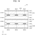
- the separation layer 25 includes a separation layer (first separation layer) 25A, a separation layer (second separation layer) 25B, and a conductive layer (third conductive layer) 25C.
- the conductive layer 25C is provided between the separation layer 25A and the separation layer 25B.
- the separation layer 25A is provided between the sensor layer 20A and the conductive layer 25C, and separates the sensor layer 20A and the conductive layer 25C.
- the separation layer 25B is provided between the sensor layer 20B and the conductive layer 25C, and separates the sensor layer 20B and the conductive layer 25C.
- the separation layer 25A and the separation layer 25B are formed to be elastically deformable in the in-plane direction of the sensing surface 20S by a shearing force acting in the in-plane direction of the sensing surface 20S (that is, the in-plane direction of the sensor 20).
- the materials of the separation layer 25A and the separation layer 25B are similar to those of the separation layer 24 in the first embodiment.
- the 25% CLD value of each of the separation layer 25A and the separation layer 25B is 10 times or more the 25% CLD value of the deformation layer 22A, preferably 30 times or more the 25% CLD value of the deformation layer 22A, and more preferably 50 times or more the 25% CLD value of the deformation layer 22A. If the 25% CLD value of each of the separation layer 25A and the separation layer 25B is 10 times or more the 25% CLD value of the deformation layer 22A, the detection sensitivity of the detection unit SE21 can be improved.
- the 25% CLD value of each of the separation layer 25A and the separation layer 25B is 10 times or more the 25% CLD value of the deformation layer 22B, preferably 30 times or more the 25% CLD value of the deformation layer 22B, and more preferably 50 times or more the 25% CLD value of the deformation layer 22B. If the 25% CLD value of each of the separation layer 25A and the separation layer 25B is 10 times or more the 25% CLD value of the deformation layer 22B, the detection sensitivity of the detection unit SE22 can be improved.
- the 25% CLD value of each of the separation layer 25A and the separation layer 25B is preferably 500 kPa or less. If the 25% CLD value of each of the separation layer 25A and the separation layer 25B exceeds 500 kPa, there is a possibility that it becomes difficult to elastically deform in the in-plane direction of the sensing surface 20S due to the shearing force acting in the in-plane direction of the sensing surface 20S (that is, the in-plane direction of the sensor 40). Therefore, there is a possibility that the detection sensitivity of the shearing force in the in-plane direction of the sensor 40 decreases.
- the 25% CLD values of the separation layer 25A and the separation layer 25B are measured in accordance with JIS K 6254.
- the conductive layer 25C is provided between the separation layer 25A and the separation layer 25B as described above, and suppresses electromagnetic interference between the sensor layer 20A and the sensor layer 20B.
- the conductive layer 25C has at least one of flexibility or stretchability. When a pressure acts on the sensing surface 20S, the conductive layer 25C bends toward the sensor layer 20B.
- the shape and material of the conductive layer 25C are similar to those of the conductive layer 23A in the first embodiment.
- Fig. 15 is a cross-sectional view for describing an example of an operation of the sensor 40 at the time of pressure detection.
- the operation of the sensor 40 at the time of pressure detection is similar to the operation of the sensor 20 at the time of pressure detection in the first embodiment except for the following points.
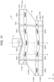
- the sensing surface 20S is pushed by the object 41 and a pressure acts on the first surface 21AS1 of the detection layer 21A by a part of the crushed deformation layer 22A, the detection layer 21A, the separation layer 25, and the detection layer 21B are bent toward the conductive layer 23B with the pressure acting portion as the center.
- Fig. 16 is a cross-sectional view for describing an example of the operation of the sensor 40 at the time of detecting a shearing force.
- the operation of the sensor 40 at the time of detecting the shearing force is similar to the operation of the sensor 40 at the time of detecting the pressure in the first embodiment except for the following points.
- the shearing force acts on the sensor 40, the separation layer 25A and the separation layer 25B are elastically deformed in the in-plane direction of the sensor 40, and the relative positions of the detection layer 21A and the detection layer 21B in the in-plane direction of the sensor 40 are shifted.
- the sensor 40 according to the second embodiment further includes the conductive layer 25C between the detection layer 21A and the detection layer 21B.
- electromagnetic interference between the detection layer 21A and the detection layer 21B can be further suppressed. Therefore, in the sensor 40, it is possible to suppress a decrease in detection accuracy or erroneous detection as compared with the sensor 20 according to the first embodiment.
- Fig. 17 is a cross-sectional view illustrating an example of a configuration of a sensor 50 according to a third embodiment of the present disclosure.
- the sensor 50 is different from the sensor 20 according to the first embodiment in including a sensor layer 50B instead of the sensor layer 20B (see Fig. 2 ).
- the sensor layer 50B includes a detection layer (second detection layer) 21B, a deformation layer (second deformation layer) 51B, a conductive layer (second conductive layer) 52B, a separation layer 53B, and a conductive layer (third conductive layer) 54B.
- the conductive layer 52B is provided to face the second surface 21BS2 of the detection layer 21B.
- the deformation layer 51B is provided between the detection layer 21B and the conductive layer 52B.
- the detection layer 21B and the conductive layer 52B are held in parallel by the deformation layer 51B.
- the conductive layer 54B is provided to face the second surface 21BS2 of the detection layer 21B.
- the separation layer 53B is provided between the detection layer 21B and the conductive layer 54B.
- the detection layer 21B and the conductive layer 54B are held in parallel by the separation layer 53B.
- the conductive layer 52B has at least one of flexibility or stretchability. When a pressure acts on the sensing surface 20S, the conductive layer 54B bends toward the detection layer 21B.
- the conductive layer 52B may or may not have at least one of flexibility or stretchability, but preferably has at least one of flexibility or stretchability in order to enable the sensor 50 to be attached to a curved surface.
- the conductive layer 52B and the conductive layer 54B are what are called grounding electrodes, and are connected to the reference potential.
- the shapes and materials of the conductive layer 52B and the conductive layer 54B are similar to those of the conductive layer 23A in the first embodiment.
- the deformation layer 51B has an insulating property.
- the deformation layer 51B separates the detection layer 21B and the conductive layer 52B so that the detection layer 21B and the conductive layer 52B are parallel.
- the sensitivity and dynamic range of the detection layer 21B can be adjusted by a thickness of the deformation layer 51B.
- the deformation layer 51B is formed to be elastically deformable according to the pressure acting on the sensing surface 20S, that is, the pressure acting in the thickness direction of the sensor 50.
- the material of the deformation layer 51B is similar to that of the deformation layer 22A in the first embodiment.
- the separation layer 53B has an insulating property.
- the separation layer 53B separates the detection layer 21B and the conductive layer 54B.
- the initial electrostatic capacitance of the sensor layer 50B is adjusted by a thickness of the separation layer 53B.
- the separation layer 53B may or may not be formed to be elastically deformable by the pressure acting on the sensing surface 20S. In a case where the separation layer 53B is formed to be elastically deformable, the pressure detection sensitivity in the sensor layer 50B can be further improved.
- the separation layer 53B formed to be elastically deformable may include a foamed resin, an insulating elastomer, or the like.
- the separation layer 53B may or may not have adhesiveness. In a case where the separation layer 53B has adhesiveness, the detection layer 21B and the conductive layer 54B are bonded by the separation layer 53B.
- the separation layer 53B having adhesiveness is formed by, for example, a single adhesive layer or a stacked body (for example, a double-sided adhesive film) in which adhesive layers are provided on both surfaces of a base material.
- the material of the adhesive layer is similar to that of the adhesive layer in the first embodiment.
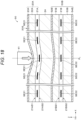
- Fig. 18 is a cross-sectional view for describing an example of operation of the sensor 50 at the time of pressure detection.
- the detection layer 21A, the separation layer 24, and the conductive layer 52B are bent toward the detection layer 21B with the pressure acting portion as the center, and a part of the deformation layer 51B is crushed.
- the conductive layer 52B and a part of the detection layer 21B approach each other. Consequently, a part of the lines of electric force of the plurality of detection units SE22 included in the part of the detection layer 21B where the conductive layer 52B approaches (that is, a part of the lines of electric force between the reception electrode 36 and the drive electrode 37) flows to the conductive layer 52B, and the capacitance of the detection unit SE22 changes.
- Fig. 19 is a cross-sectional view for describing an example of operation of the sensor 50 at the time of detecting a shearing force.
- the separation layer 24 is elastically deformed in the in-plane direction of the sensor 50, and the relative positions of the detection unit SE21 and the detection unit SE22 in the in-plane direction (X, Y direction) of the sensor 50 are shifted.
- the centroid position of the output signal distribution (capacitance distribution) of the detection layer 21A and the centroid position of the output signal distribution (capacitance distribution) of the detection layer 21B are shifted in the in-plane direction (X, Y direction) of the sensor 50.
- the sensor 50 according to the third embodiment includes the deformation layer 51B on the detection layer 21B. Therefore, the detection sensitivity of the pressure and the shearing force can be improved as compared with the sensor 20 according to the first embodiment including the deformation layer 22B below the detection layer 21B.
- Fig. 20 is a cross-sectional view illustrating an example of a configuration of a sensor 60 according to a fourth embodiment of the present disclosure.
- the sensor 60 is different from the sensor 50 according to the third embodiment in including a sensor layer 60A instead of the sensor layer (first sensor layer) 20A.
- the same reference numerals are given to parts similar to those in the third embodiment, and the description thereof will be omitted.
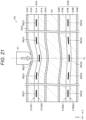
- Fig. 21 is a cross-sectional view for describing an example of operation of the sensor 60 at the time of pressure detection.
- an example of the operation of the sensor 60 at the time of pressure detection will be described for a case where the separation layers 61A and 53B are formed to be elastically deformable by the pressure acting on the sensing surface 20S.
- the sensing surface 20S is pressed by the object 41 and a pressure acts on the sensing surface 20S
- the conductive layer 23A and a part of the detection layer 21A approach each other, similarly to the operation of the sensor 20 in the first embodiment.
- a pressure acts on the first surface 21AS1 of the detection layer 21A by a part of the deformation layer 22A crushed by the conductive layer 23A
- the detection layer 21A bends toward the conductive layer 62A with the pressure acting portion as the center, and crushes a part of the separation layer 61A.
- the detection layer 21A and the part of the conductive layer 62A approach each other.
- a part of lines of electric force of the plurality of detection units SE21 included in the portion close to the conductive layer 23A and the conductive layer 62A flows to the conductive layer 23A and the conductive layer 62A, and the electrostatic capacitance of the plurality of detection units SE21 changes.
- the conductive layer 62A, the separation layer 24, and the conductive layer 52B are bent toward the detection layer 21B with the pressure acting portion as the center, and a part of the deformation layer 51B is crushed.
- the conductive layer 52B and a part of the detection layer 21B approach each other.
- the detection layer 21B bends toward the conductive layer 54B around the pressure acting portion and crushes a part of the separation layer 53B.
- the detection layer 21B and a part of the conductive layer 54B approach each other.
- Fig. 22 is a cross-sectional view for describing an example of operation of the sensor 60 at a time of detecting a shearing force.
- the separation layer 24 is elastically deformed in the in-plane direction of the sensor 60, and the relative positions of the detection unit SE21 and the detection unit SE22 in the in-plane direction (X, Y direction) of the sensor 60 are shifted.
- the centroid position of the output signal distribution (capacitance distribution) of the detection layer 21A and the centroid position of the output signal distribution (capacitance distribution) of the detection layer 21B are shifted in the in-plane direction (X, Y direction) of the sensor 60.
- Fig. 24A is a graph illustrating an example of a load sensitivity curve of the sensor 70.
- Fig. 24B is an enlarged graph illustrating a part of Fig. 24A (near a boundary between a low load region and a high load region).
- the sensor layer 70A is for a low load region (for a first load region).
- the sensor layer 70B is for a high load region (for a second load region).
- the low load region is a pressure range of a prescribed pressure P or less.
- the high load region is a pressure range exceeding a prescribed pressure P.
- the prescribed pressure P is set to a boundary value at which a load sensitivity curve of the sensor layer 70A as an upper layer starts to be saturated.
- the boundary value may be, for example, an inflection point.
- Figs. 24A and 24B illustrate an example in which the prescribed pressure P is 100 kPa.
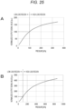
- Fig. 25A is a graph illustrating an example of a load sensitivity curve (hereinafter referred to as a "low load sensitivity curve") of the sensor layer 70A.
- Fig. 25B is a graph illustrating an example of a load sensitivity curve (hereinafter referred to as a "high load sensitivity curve”) of the sensor layer 70B.
- the low load sensitivity curve of the sensor layer 70A as the upper layer starts to be saturated at a pressure of 100 kPa. Accordingly, in Figs. 25A and 25B , an output signal value is normalized such that the output signal value at the pressure of 100 kPa becomes 100. This normalization processing is performed by the CPU 12A.
- the CPU 12A normalizes a first output signal value from the sensor layer 70A and a second output signal value from the sensor layer 70B as described above.
- the CPU 12A determines whether or not the normalized first output signal value exceeds a prescribed output signal value.
- the prescribed output signal value means an output signal value corresponding to the prescribed pressure P described above.
- Figs. 24A and 24B illustrate an example in which the output signal value is 100. Note that the IC 13A may output the normalized first output signal value and the second output signal to the CPU 12A after performing the normalization processing described above.
- the sensor 70 according to the fifth embodiment includes the sensor layer 70A having high sensitivity and the sensor layer 70B having low sensitivity, and the sensor layer 70A is provided on the sensor layer 70B.
- the load (pressure distribution) in the low load region can be detected by the sensor layer 70A
- the load (pressure distribution) in the high load region can be detected by the sensor layer 70B. Therefore, it is possible to complement the dynamic ranges of the sensor layers 70A and 70B with each other while suppressing a decrease in sensitivity of the sensor 70.
- Fig. 27 is a cross-sectional view illustrating an example of a configuration of a sensor 80 according to a sixth embodiment of the present disclosure.
- the sensor 80 is a pressure distribution sensor having a temperature compensation function, and includes a pressure sensor layer 80A (hereinafter simply referred to as a "sensor layer 80A") that detects a pressure distribution and a temperature detection sensor layer 80B (hereinafter simply referred to as a "sensor layer 80B”) that detects an environmental temperature of the sensor 80.
- the sensor layer 80A is provided on the sensor layer 80B.
- the sensor layer 80A has a configuration similar to that of the sensor layer 60A (see Fig. 20 ) in the fourth embodiment except that the sensor layer 80A does not include the conductive layer 62A.
- the sensor layer 80A detects a distribution of pressure acting on the sensing surface 20S and outputs the distribution of pressure to the IC 13A.
- the sensor layer 80B is different from the sensor layer 50B in the fourth embodiment in including a separation layer 81B in place of the deformation layer 51B and including a separation layer 82B in place of the separation layer 53B (see Fig. 20 ).
- the sensor layer 80B detects a change in electrostatic capacitance according to a change in environmental temperature of the sensor 80, and outputs the change to the IC 13A.
- the separation layers 81B and 82B are formed to be capable of maintaining a thickness substantially constant with little deformation even when a pressure acts on the sensing surface 20S.
- the distance between the detection layer 21B and the conductive layer 52B is held substantially constant, and the distance between the detection layer 21B and the conductive layer 54B is held substantially constant. Therefore, even when a pressure acts on the sensing surface 20S, the capacitance of the detection layer 21B hardly changes.
- a dielectric constant (temperature factor) of a member (for example, at least one of the base material 31 or the adhesive layer 35A (see Fig. 4 )) provided around the detection unit SE21 is a low dielectric constant
- a dielectric constant (temperature factor) of a member (for example, at least one of the base material 31 or the adhesive layer 35A (see Fig. 4 )) provided around the detection unit SE22 is a high dielectric constant.
- a dielectric constant of a member for example, at least one of the base material 31 or the adhesive layer 35A (see Fig. 4 )
- a dielectric constant of a member for example, at least one of the base material 31 or the adhesive layer 35A (see Fig. 4 )
- a dielectric constant of a member for example, at least one of the base material 31 or the adhesive layer 35A (see Fig. 4 )
- each of the plurality of detection units SE22 is preferably provided corresponding to the detection unit SE21.
- the plurality of detection units SE22 included in the sensor layer 80B may be provided so as to overlap the plurality of detection units SE21 included in the sensor layer 80A, respectively, in the thickness direction (Z-axis direction) of the sensor 80.
- the CPU 12A corrects the first output signal (that is, the first capacitance distribution) from the IC 13A on the basis of the second output signal (that is, the second capacitance distribution) from the IC 13A.
- the CPU 12A calculates centroid coordinates of the pressure acting on the detection layer 21A on the basis of the corrected first output signal, and executes various controls of the host device 12 on the basis of a calculation result. Examples of a method for correcting the first output signal include a method described in WO 2018/186022 .
- the sensor 80 according to the sixth embodiment includes a sensor layer 80A and a sensor layer 80B, and the sensor layer 80A is provided on the sensor layer 80B.
- the plurality of detection units SE22 for detecting the temperature of the sensor 80 is provided, an increase in the area of the sensor 80 can be suppressed. Therefore, it is possible to achieve temperature compensation of the sensor 80 while suppressing an increase in the area of the sensor 80.
- a pressure distribution sensor ( WO 2018/186022 ) in which a detection unit for temperature detection is arranged near a detection unit for pressure detection and temperature compensation is performed, since the detection unit for temperature detection is provided, the area of the sensor increases.
- Fig. 28 is a cross-sectional view illustrating an example of a configuration of a sensor 90 according to a seventh embodiment of the present disclosure.
- the sensor 90 is a pressure distribution sensor and includes a sensor layer 90A and a sensor layer 90B, and the sensor layer 90A is provided on the sensor layer 90B.
- the sensor layer 90A has a configuration similar to that of the sensor layer 60A (see Fig. 20 ) in the fourth embodiment except that the sensor layer 90A does not include the conductive layer 62A.
- the sensor layer 90B has a configuration similar to that of the sensor layer 50B (see Fig. 17 ) in the third embodiment except that the plurality of detection units SE22 is arranged to be shifted respectively in the in-plane direction of the sensor 90 with respect to the plurality of detection units SE21.
- Fig. 29 is a plan view illustrating a positional relationship between the plurality of detection units SE21 included in the sensor layer 90A and the plurality of detection units SE22 included in the sensor layer 90B.
- the plurality of detection units SE21 and the plurality of detection units SE22 are arranged at an arrangement pitch P in the row direction (X-axis direction) and the column direction (Y-axis direction) of the matrix array.
- the detection units SE22 are arranged to be shifted from the detection units SE21 by P/2 in each of the row direction (X-axis direction) and the column direction (Y-axis direction) of the matrix array.
- One-fourth size regions of the detection units SE21 and one-fourth size regions of the detection units SE22 overlap in the thickness direction of the sensor 90.
- Virtual detection units SE90 are formed by portions where these one-fourth size regions overlap.
- the detection units SE22 are arranged to be shifted by P/2 in the row direction (X-axis direction) and the column direction (Y-axis direction) with respect to the detection units SE21 will be described, but it is sufficient if the detection units SE21 and the detection units SE22 overlap each other in the thickness direction of the sensor 90, and the shift amount of the detection units SE22 is not limited to P/2.
- the CPU 12A calculates output signals (electrostatic capacitance distribution) of the plurality of virtual detection units SE21 on the basis of the first output signals (that is, a first electrostatic capacitance distribution) of the plurality of detection units SE22 and the second output signals (that is, a second electrostatic capacitance distribution) of the plurality of detection units SE90 supplied from the IC 13A.
- the CPU 12A calculates centroid coordinates of the pressure acting on the sensor 90 on the basis of the calculated output signal (capacitance distribution), and executes various controls of the host device 12 on the basis of the calculation result.
- Fig. 30A is a graph illustrating an example of a load sensitivity curve (hereinafter referred to as a "first load sensitivity curve”) of the sensor layer 90A.
- Fig. 30B is a graph illustrating an example of a load sensitivity curve (hereinafter referred to as a "second load sensitivity curve”) of the sensor layer 90B.
- the CPU 12A normalizes the output signal value supplied from the sensor layer 90A and the output signal value supplied from the sensor layer 90B, and performs processing so that the output signal values for the same pressure value are the same or substantially the same.
- Fig. 31A illustrates a first load sensitivity curve normalized such that the output signal value becomes 1000 at a pressure of 175 kPa.
- Fig. 31B illustrates a second load sensitivity curve normalized such that the output signal value becomes 1000 at a pressure of 175 kPa.
- the pressure 175 kPa used for normalization is a pressure value around the maximum value of the detection range of the sensor layer 90A.
- Fig. 32A is a schematic diagram of the plurality of detection units SE21 included in the sensor layer 90A.
- Fig. 32B is a schematic diagram of the plurality of detection units SE22 included in the sensor layer 90B.
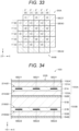
- Fig. 33 is a schematic diagram illustrating a positional relationship between the detection units SE21 and SE22 in a state where the sensor layers 90A and 90B are overlapped.
- the detection units SE21 are referred to as detection units (1) to (9) using reference numerals (1) to (9). Furthermore, in a case of distinguishing the detection units SE22 included in the sensor layer 90B, as illustrated in Fig. 32B , the detection units SE22 are referred to as detection units ⁇ 1> to ⁇ 9> using reference numerals ⁇ 1> to ⁇ 9>.
- each of the detection units SE21 and SE22 is indicated by coordinates (X[m], Y[n]) (where m and n are integers of 0 or more and 2 or less).
- the center position of each virtual detection unit SE90 is indicated by coordinates (X'[m'], Y'[n']) (where m' and n' are integers of 0 or more and 4 or less).
- the output signal value of each virtual detection unit SE90 is calculated by the following equation.
- Output signal value of virtual detection unit (X'[0], Y'[0]) (normalized output signal value of detection unit (1) + normalized output signal value of detection unit ⁇ 1>)/2
- Output signal value of virtual detection unit (X'[0], Y'[1]) (normalized output signal value of detection unit (1) + normalized output signal value of detection unit ⁇ 2>)/2
- Output signal value of virtual detection unit (X'[0], Y'[2]) (normalized output signal value of detection unit (2) + normalized output signal value of detection unit ⁇ 2>)/2
- Output signal value of virtual detection unit (X'[1], Y'[0]) (normalized output signal value of detection unit (4) + normalized output signal value of detection unit ⁇ 1>)/2
- Output signal value of virtual detection unit (X'[1], Y'[1]) (normalized output signal value of detection unit (4) + normalized output signal value of detection unit
- the seventh embodiment is similar to the first embodiment except for the above.
- the sensor 100 includes a sensor layer 100A and a sensor layer 100B, and the sensor layer 100A is provided on the sensor layer 100B.
- the CPU 12A detects a proximity operation and a touch operation on the sensing surface 20S on the basis of the first output signal (that is, the first capacitance distribution) of the sensor layer 100A supplied from the IC 13A, and executes various controls of the host device 12 on the basis of the detection result. Furthermore, the CPU 12A detects a push-in operation on the sensing surface 20S on the basis of the second output signal (that is, the second capacitance distribution) of the sensor layer 100B supplied from the IC 13A, and executes various controls of the host device 12 on the basis of the detection result.
- the surface layer 104A may have an irregularity shape on a surface to achieve the surface having a high friction coefficient
- the surface layer 104A may contain a rubber-based resin (for example, silicone rubber) to achieve the surface having a high friction coefficient
- the surface layer 104A may have the irregularity shape on a surface and the surface layer 104A may contain the rubber-based resin to achieve the surface having a high friction coefficient.
- a static friction coefficient of the surface of the surface layer 104A is preferably 1 or more from the viewpoint of suppressing sliding of an object on the sensing surface 20S of the sensor 20.
- the static friction coefficient is measured in accordance with JIS K 7125: 1999 using a friction coefficient measuring jig manufactured by IMADA Co., Ltd.
- the surface layer 104A may be an exterior member of an electronic device or the like.
- reception electrode 36 and the drive electrode 37 are provided on the first surface 31S1 of the base material 31
- the reception electrode 36 and the drive electrode 37 may be provided on different surfaces of the base material 31.
- the reception electrode 36 may be provided on the first surface 31S1 of the base material
- the drive electrode 37 may be provided on the second surface 31S2 of the base material
- the reception electrode 36 and the drive electrode 37 may face each other with the base material 31 interposed therebetween.
- the case where the sensor layers 20A, 20B, 50B, 60A, 70A, 80A, 80B, 90A, 90B, 100A, and 100B (hereinafter referred to as "sensor layers 20A, 20B, and so on") are mutual capacitive sensor layers has been described, but the sensor layers 20A and 20B and the like may be self-capacitive sensor layers.
- the sensor layers 20A and 20B and the like include a base material and a thin-film electrode layer provided on the base material.
- the sensor layers 20A and 20B and the like are capacitance type sensor layers has been described, but the sensor layers 20A and 20B and the like may be sensor layers of a type other than the capacitance type.
- the detection layer 21A and the detection layer 21B may be configured by one flexible printed circuit board.
- the configurations of the sensors 20, 40, 50, 60, 70, 80, and 90 can be simplified.
- the flexible printed circuit board described above may be folded back between the region including the detection layer 21A and the region including the detection layer 21B, and overlapped with the separation layer 24, the separation layer 25, or the like interposed therebetween.
- At least one of the sensors 20, 40, 50, 60, 70, 80, 90, or 100 according to the first to eighth embodiments and their modification examples can be applied to various electronic devices.
- a mobile phone such as a personal computer or a smartphone, a television, a remote controller, a camera, a game device, a navigation system, an electronic book, an electronic dictionary, a portable music player, a keyboard, a wearable terminal, a radio, a stereo, a medical device, a robot, or the like.
- Examples of the wearable terminal include a smart watch, a head-mounted display, a wristband, a ring, glasses, shoes, clothes, and the like.
- At least one of the sensors 20, 40, 50, 60, 70, 80, 90, or 100 according to the first to eighth embodiments and their modification examples can be applied to various devices other than electronic devices.
- an electric device such as an electric power tool, a refrigerator, an air conditioner, a water heater, a microwave oven, a dishwasher, a washing machine, a dryer, a lighting device, or a toy.
- buildings including houses, building members, vehicles, furniture such as tables and desks, manufacturing devices, analytical instruments, and the like.
- Examples of the construction member include a paving stone, a wall member, a floor tile, a floor board, and the like.
- the vehicle include a vehicle (for example, an automobile, a motorcycle, or the like), a ship, a submarine, a railway vehicle, an aircraft, a spacecraft, an elevator, playground equipment, and the like.
- At least one of the sensors 20, 40, 50, 60, 70, 80, 90, or 100 according to the first to eighth embodiments and their modification examples may be applied to a robot hand.
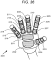
- Fig. 36 illustrates a configuration of a robot hand 200 to which sensors 201 to 216 is applied.
- the sensors 201 to 216 are any one of the sensors 20, 40, 50, 60, 70, 80, 90, and 100 according to the first to eighth embodiments and their modification examples.
- the sensors 201 and 202 are provided in a palm constituting the robot hand 200, the sensor 203 is provided above a first joint on a palm surface of the thumb constituting the robot hand 200, the sensor 204 is provided between the first joint and a second joint, the sensor 205 is provided above a first joint on a palm surface of the index finger, the sensor 206 is provided between the first joint and a second joint, and the sensor 207 is provided between the second joint and a third joint.
- the senor 208 is provided above a first joint on a palm surface of the middle finger
- the sensor 209 is provided between the first joint and a second joint
- the sensor 210 is provided between the second joint and a third joint
- the sensor 211 is provided above a first joint on a palm surface of the ring finger
- the sensor 212 is provided between the first joint and a second joint
- the sensor 213 is provided between the second joint and a third joint
- the sensor 214 is provided above a first joint on a palm surface of the little finger
- the sensor 215 is provided between the first joint and a second joint
- the sensor 216 is provided between the second joint and a third joint.
Landscapes
- Engineering & Computer Science (AREA)
- General Engineering & Computer Science (AREA)
- Theoretical Computer Science (AREA)
- Human Computer Interaction (AREA)
- Physics & Mathematics (AREA)
- General Physics & Mathematics (AREA)
- Computer Networks & Wireless Communication (AREA)
- Force Measurement Appropriate To Specific Purposes (AREA)
Applications Claiming Priority (2)
| Application Number | Priority Date | Filing Date | Title |
|---|---|---|---|
| JP2020015400 | 2020-01-31 | ||
| PCT/JP2021/003126 WO2021153700A1 (ja) | 2020-01-31 | 2021-01-29 | センサモジュールおよび電子機器 |
Publications (3)
| Publication Number | Publication Date |
|---|---|
| EP4086738A1 EP4086738A1 (en) | 2022-11-09 |
| EP4086738A4 EP4086738A4 (en) | 2023-06-28 |
| EP4086738B1 true EP4086738B1 (en) | 2025-07-02 |
Family
ID=77079385
Family Applications (1)
| Application Number | Title | Priority Date | Filing Date |
|---|---|---|---|
| EP21748140.7A Active EP4086738B1 (en) | 2020-01-31 | 2021-01-29 | Sensor module, and electronic instrument |
Country Status (4)
| Country | Link |
|---|---|
| US (1) | US11966550B2 (https=) |
| EP (1) | EP4086738B1 (https=) |
| JP (1) | JP7567814B2 (https=) |
| WO (1) | WO2021153700A1 (https=) |
Families Citing this family (5)
| Publication number | Priority date | Publication date | Assignee | Title |
|---|---|---|---|---|
| CN116710742A (zh) * | 2021-01-27 | 2023-09-05 | 索尼集团公司 | 力传感器模块 |
| US20250128425A1 (en) * | 2021-09-22 | 2025-04-24 | Sony Group Corporation | Robot apparatus and control method therefor |
| JP7500147B1 (ja) | 2022-12-19 | 2024-06-17 | Nissha株式会社 | 押圧力及び引張力を検出するコントローラー |
| JP2024116908A (ja) * | 2023-02-16 | 2024-08-28 | 株式会社ワコム | 電子機器、集積回路、及び入力システム |
| TWI884707B (zh) * | 2024-02-17 | 2025-05-21 | 友達光電股份有限公司 | 顯示器及顯示方法 |
Family Cites Families (15)
| Publication number | Priority date | Publication date | Assignee | Title |
|---|---|---|---|---|
| JP5003336B2 (ja) | 2007-07-31 | 2012-08-15 | ソニー株式会社 | 検出装置、ロボット装置、および入力装置 |
| TWM422118U (en) * | 2010-12-30 | 2012-02-01 | Egalax Empia Technology Inc | Capacitive touch screen |
| EP2836960B1 (en) * | 2012-04-10 | 2018-09-26 | Idex Asa | Biometric sensing |
| KR102061569B1 (ko) | 2013-05-16 | 2020-01-03 | 삼성디스플레이 주식회사 | 표시장치 및 표시장치의 구동방법 |
| JP2015056005A (ja) * | 2013-09-11 | 2015-03-23 | ソニー株式会社 | センサ装置、入力装置及び電子機器 |
| EP3227730A4 (en) * | 2014-12-03 | 2018-08-01 | University Of British Columbia | Flexible transparent sensor with ionically-conductive material |
| KR20160086689A (ko) * | 2015-01-12 | 2016-07-20 | 삼성전기주식회사 | 바디 터치 디바이스 |
| CN106325631B (zh) * | 2015-07-10 | 2023-03-07 | 宸鸿科技(厦门)有限公司 | 一种具有压力侦测的触控显示模组及其驱动方法 |
| US20190004625A1 (en) | 2015-10-29 | 2019-01-03 | Hewlett-Packard Development Company ,L.P. | Touch device |
| US10372259B2 (en) * | 2016-02-19 | 2019-08-06 | Synaptics Incorporated | Transcapacitive touch and force sensing in an input device |
| US10067590B2 (en) * | 2016-04-29 | 2018-09-04 | Synaptics Incorporated | Differential force and touch sensing |
| US10719159B2 (en) * | 2017-03-17 | 2020-07-21 | Synaptics Incorporated | Method and system for force sensitive components in a display device |
| CN110462563B (zh) | 2017-04-03 | 2023-09-01 | 索尼公司 | 传感器、输入装置、和电子设备 |
| GB2565305A (en) * | 2017-08-08 | 2019-02-13 | Cambridge Touch Tech Ltd | Device for processing signals from a pressure-sensing touch panel |
| TWI671509B (zh) | 2018-01-05 | 2019-09-11 | 財團法人工業技術研究院 | 觸覺感測器 |
-
2021
- 2021-01-29 WO PCT/JP2021/003126 patent/WO2021153700A1/ja not_active Ceased
- 2021-01-29 EP EP21748140.7A patent/EP4086738B1/en active Active
- 2021-01-29 JP JP2021574129A patent/JP7567814B2/ja active Active
- 2021-01-29 US US17/790,396 patent/US11966550B2/en active Active
Non-Patent Citations (1)
| Title |
|---|
| YURIKO NAKAI ET AL: "Detection of tangential force for a touch panel using shear deformation of the gel", 20140426; 1077952576 - 1077952576, 26 April 2014 (2014-04-26), pages 2353 - 2358, XP058047710, ISBN: 978-1-4503-2474-8, DOI: 10.1145/2559206.2581149 * |
Also Published As
| Publication number | Publication date |
|---|---|
| US20230043375A1 (en) | 2023-02-09 |
| WO2021153700A1 (ja) | 2021-08-05 |
| US11966550B2 (en) | 2024-04-23 |
| EP4086738A4 (en) | 2023-06-28 |
| JPWO2021153700A1 (https=) | 2021-08-05 |
| JP7567814B2 (ja) | 2024-10-16 |
| EP4086738A1 (en) | 2022-11-09 |
Similar Documents
| Publication | Publication Date | Title |
|---|---|---|
| EP4086738B1 (en) | Sensor module, and electronic instrument | |
| TWI662462B (zh) | 感測裝置,輸入裝置及電子設備 | |
| US9959444B2 (en) | Fingerprint sensor under thin face-sheet with aperture layer | |
| CN104025000B (zh) | 单衬底触摸传感器 | |
| US9632637B2 (en) | Sensor device, input device, and electronic apparatus | |
| EP2983067B1 (en) | Input device and electronic apparatus | |
| JP7509154B2 (ja) | 3軸センサ、センサモジュールおよび電子機器 | |
| US20120212445A1 (en) | Display With Rear Side Capacitive Touch Sensing | |
| CN105531651B (zh) | 传感器装置、输入装置和电子设备 | |
| US10394339B2 (en) | Sensor, input device, keyboard, and electronic device | |
| US20220034728A1 (en) | Sensor, stack-type sensor, and electronic device | |
| US10754478B2 (en) | Capacitive display device | |
| EP3499348A1 (en) | Sensor, input device and electronic device | |
| US10324569B2 (en) | Touch sensing unit, touch screen panel having the same, and method of driving the touch screen panel | |
| US20170185219A1 (en) | Touch screen display device | |
| US20250284361A1 (en) | Electronic device | |
| US20240329785A1 (en) | Electronic device | |
| CN109478114B (zh) | 传感器和电子设备 | |
| Seomoon et al. | 35‐4: High Sensitive Pen Writing Solution Based on Mechanical Sensing |
Legal Events
| Date | Code | Title | Description |
|---|---|---|---|
| STAA | Information on the status of an ep patent application or granted ep patent |
Free format text: STATUS: THE INTERNATIONAL PUBLICATION HAS BEEN MADE |
|
| PUAI | Public reference made under article 153(3) epc to a published international application that has entered the european phase |
Free format text: ORIGINAL CODE: 0009012 |
|
| STAA | Information on the status of an ep patent application or granted ep patent |
Free format text: STATUS: REQUEST FOR EXAMINATION WAS MADE |
|
| 17P | Request for examination filed |
Effective date: 20220714 |
|
| AK | Designated contracting states |
Kind code of ref document: A1 Designated state(s): AL AT BE BG CH CY CZ DE DK EE ES FI FR GB GR HR HU IE IS IT LI LT LU LV MC MK MT NL NO PL PT RO RS SE SI SK SM TR |
|
| DAV | Request for validation of the european patent (deleted) | ||
| DAX | Request for extension of the european patent (deleted) | ||
| A4 | Supplementary search report drawn up and despatched |
Effective date: 20230531 |
|
| RIC1 | Information provided on ipc code assigned before grant |
Ipc: G06F 3/044 20060101ALI20230524BHEP Ipc: G06F 3/041 20060101AFI20230524BHEP |
|
| STAA | Information on the status of an ep patent application or granted ep patent |
Free format text: STATUS: EXAMINATION IS IN PROGRESS |
|
| 17Q | First examination report despatched |
Effective date: 20231128 |
|
| GRAP | Despatch of communication of intention to grant a patent |
Free format text: ORIGINAL CODE: EPIDOSNIGR1 |
|
| STAA | Information on the status of an ep patent application or granted ep patent |
Free format text: STATUS: GRANT OF PATENT IS INTENDED |
|
| INTG | Intention to grant announced |
Effective date: 20250204 |
|
| GRAS | Grant fee paid |
Free format text: ORIGINAL CODE: EPIDOSNIGR3 |
|
| GRAA | (expected) grant |
Free format text: ORIGINAL CODE: 0009210 |
|
| STAA | Information on the status of an ep patent application or granted ep patent |
Free format text: STATUS: THE PATENT HAS BEEN GRANTED |
|
| P01 | Opt-out of the competence of the unified patent court (upc) registered |
Free format text: CASE NUMBER: APP_22619/2025 Effective date: 20250513 |
|
| AK | Designated contracting states |
Kind code of ref document: B1 Designated state(s): AL AT BE BG CH CY CZ DE DK EE ES FI FR GB GR HR HU IE IS IT LI LT LU LV MC MK MT NL NO PL PT RO RS SE SI SK SM TR |
|
| REG | Reference to a national code |
Ref country code: GB Ref legal event code: FG4D |
|
| REG | Reference to a national code |
Ref country code: CH Ref legal event code: EP |
|
| REG | Reference to a national code |
Ref country code: DE Ref legal event code: R096 Ref document number: 602021033398 Country of ref document: DE |
|
| REG | Reference to a national code |
Ref country code: IE Ref legal event code: FG4D |
|
| REG | Reference to a national code |
Ref country code: NL Ref legal event code: MP Effective date: 20250702 |
|
| PG25 | Lapsed in a contracting state [announced via postgrant information from national office to epo] |
Ref country code: PT Free format text: LAPSE BECAUSE OF FAILURE TO SUBMIT A TRANSLATION OF THE DESCRIPTION OR TO PAY THE FEE WITHIN THE PRESCRIBED TIME-LIMIT Effective date: 20251103 |
|
| PG25 | Lapsed in a contracting state [announced via postgrant information from national office to epo] |
Ref country code: NL Free format text: LAPSE BECAUSE OF FAILURE TO SUBMIT A TRANSLATION OF THE DESCRIPTION OR TO PAY THE FEE WITHIN THE PRESCRIBED TIME-LIMIT Effective date: 20250702 |
|
| REG | Reference to a national code |
Ref country code: AT Ref legal event code: MK05 Ref document number: 1809981 Country of ref document: AT Kind code of ref document: T Effective date: 20250702 |
|
| PG25 | Lapsed in a contracting state [announced via postgrant information from national office to epo] |
Ref country code: IS Free format text: LAPSE BECAUSE OF FAILURE TO SUBMIT A TRANSLATION OF THE DESCRIPTION OR TO PAY THE FEE WITHIN THE PRESCRIBED TIME-LIMIT Effective date: 20251102 |
|
| PG25 | Lapsed in a contracting state [announced via postgrant information from national office to epo] |
Ref country code: NO Free format text: LAPSE BECAUSE OF FAILURE TO SUBMIT A TRANSLATION OF THE DESCRIPTION OR TO PAY THE FEE WITHIN THE PRESCRIBED TIME-LIMIT Effective date: 20251002 |
|
| REG | Reference to a national code |
Ref country code: LT Ref legal event code: MG9D |
|
| PG25 | Lapsed in a contracting state [announced via postgrant information from national office to epo] |
Ref country code: AT Free format text: LAPSE BECAUSE OF FAILURE TO SUBMIT A TRANSLATION OF THE DESCRIPTION OR TO PAY THE FEE WITHIN THE PRESCRIBED TIME-LIMIT Effective date: 20250702 |
|
| PG25 | Lapsed in a contracting state [announced via postgrant information from national office to epo] |
Ref country code: FI Free format text: LAPSE BECAUSE OF FAILURE TO SUBMIT A TRANSLATION OF THE DESCRIPTION OR TO PAY THE FEE WITHIN THE PRESCRIBED TIME-LIMIT Effective date: 20250702 |
|
| PG25 | Lapsed in a contracting state [announced via postgrant information from national office to epo] |
Ref country code: HR Free format text: LAPSE BECAUSE OF FAILURE TO SUBMIT A TRANSLATION OF THE DESCRIPTION OR TO PAY THE FEE WITHIN THE PRESCRIBED TIME-LIMIT Effective date: 20250702 |
|
| PG25 | Lapsed in a contracting state [announced via postgrant information from national office to epo] |
Ref country code: GR Free format text: LAPSE BECAUSE OF FAILURE TO SUBMIT A TRANSLATION OF THE DESCRIPTION OR TO PAY THE FEE WITHIN THE PRESCRIBED TIME-LIMIT Effective date: 20251003 |
|
| PG25 | Lapsed in a contracting state [announced via postgrant information from national office to epo] |
Ref country code: SE Free format text: LAPSE BECAUSE OF FAILURE TO SUBMIT A TRANSLATION OF THE DESCRIPTION OR TO PAY THE FEE WITHIN THE PRESCRIBED TIME-LIMIT Effective date: 20250702 Ref country code: CZ Free format text: LAPSE BECAUSE OF FAILURE TO SUBMIT A TRANSLATION OF THE DESCRIPTION OR TO PAY THE FEE WITHIN THE PRESCRIBED TIME-LIMIT Effective date: 20250702 |
|
| PG25 | Lapsed in a contracting state [announced via postgrant information from national office to epo] |
Ref country code: LV Free format text: LAPSE BECAUSE OF FAILURE TO SUBMIT A TRANSLATION OF THE DESCRIPTION OR TO PAY THE FEE WITHIN THE PRESCRIBED TIME-LIMIT Effective date: 20250702 |
|
| PG25 | Lapsed in a contracting state [announced via postgrant information from national office to epo] |
Ref country code: BG Free format text: LAPSE BECAUSE OF FAILURE TO SUBMIT A TRANSLATION OF THE DESCRIPTION OR TO PAY THE FEE WITHIN THE PRESCRIBED TIME-LIMIT Effective date: 20250702 Ref country code: PL Free format text: LAPSE BECAUSE OF FAILURE TO SUBMIT A TRANSLATION OF THE DESCRIPTION OR TO PAY THE FEE WITHIN THE PRESCRIBED TIME-LIMIT Effective date: 20250702 |
|
| PG25 | Lapsed in a contracting state [announced via postgrant information from national office to epo] |
Ref country code: RS Free format text: LAPSE BECAUSE OF FAILURE TO SUBMIT A TRANSLATION OF THE DESCRIPTION OR TO PAY THE FEE WITHIN THE PRESCRIBED TIME-LIMIT Effective date: 20251002 |
|
| PG25 | Lapsed in a contracting state [announced via postgrant information from national office to epo] |
Ref country code: ES Free format text: LAPSE BECAUSE OF FAILURE TO SUBMIT A TRANSLATION OF THE DESCRIPTION OR TO PAY THE FEE WITHIN THE PRESCRIBED TIME-LIMIT Effective date: 20250702 |
|
| PG25 | Lapsed in a contracting state [announced via postgrant information from national office to epo] |
Ref country code: SM Free format text: LAPSE BECAUSE OF FAILURE TO SUBMIT A TRANSLATION OF THE DESCRIPTION OR TO PAY THE FEE WITHIN THE PRESCRIBED TIME-LIMIT Effective date: 20250702 |
|
| PG25 | Lapsed in a contracting state [announced via postgrant information from national office to epo] |
Ref country code: DK Free format text: LAPSE BECAUSE OF FAILURE TO SUBMIT A TRANSLATION OF THE DESCRIPTION OR TO PAY THE FEE WITHIN THE PRESCRIBED TIME-LIMIT Effective date: 20250702 |
|
| PGFP | Annual fee paid to national office [announced via postgrant information from national office to epo] |
Ref country code: DE Payment date: 20251217 Year of fee payment: 6 |
|
| PG25 | Lapsed in a contracting state [announced via postgrant information from national office to epo] |
Ref country code: IT Free format text: LAPSE BECAUSE OF FAILURE TO SUBMIT A TRANSLATION OF THE DESCRIPTION OR TO PAY THE FEE WITHIN THE PRESCRIBED TIME-LIMIT Effective date: 20250702 |
|
| PG25 | Lapsed in a contracting state [announced via postgrant information from national office to epo] |
Ref country code: EE Free format text: LAPSE BECAUSE OF FAILURE TO SUBMIT A TRANSLATION OF THE DESCRIPTION OR TO PAY THE FEE WITHIN THE PRESCRIBED TIME-LIMIT Effective date: 20250702 Ref country code: SK Free format text: LAPSE BECAUSE OF FAILURE TO SUBMIT A TRANSLATION OF THE DESCRIPTION OR TO PAY THE FEE WITHIN THE PRESCRIBED TIME-LIMIT Effective date: 20250702 |