EP4084331A1 - Synchrone gleichrichtung zum abschwächen des rail-pumpens in einem unsymmetrischen class-d-verstärker - Google Patents
Synchrone gleichrichtung zum abschwächen des rail-pumpens in einem unsymmetrischen class-d-verstärker Download PDFInfo
- Publication number
- EP4084331A1 EP4084331A1 EP22170032.1A EP22170032A EP4084331A1 EP 4084331 A1 EP4084331 A1 EP 4084331A1 EP 22170032 A EP22170032 A EP 22170032A EP 4084331 A1 EP4084331 A1 EP 4084331A1
- Authority
- EP
- European Patent Office
- Prior art keywords
- mosfet
- voltage rail
- diode
- voltage
- rail
- Prior art date
- Legal status (The legal status is an assumption and is not a legal conclusion. Google has not performed a legal analysis and makes no representation as to the accuracy of the status listed.)
- Withdrawn
Links
Images



Classifications
-
- H—ELECTRICITY
- H02—GENERATION; CONVERSION OR DISTRIBUTION OF ELECTRIC POWER
- H02M—APPARATUS FOR CONVERSION BETWEEN AC AND AC, BETWEEN AC AND DC, OR BETWEEN DC AND DC, AND FOR USE WITH MAINS OR SIMILAR POWER SUPPLY SYSTEMS; CONVERSION OF DC OR AC INPUT POWER INTO SURGE OUTPUT POWER; CONTROL OR REGULATION THEREOF
- H02M3/00—Conversion of DC power input into DC power output
- H02M3/22—Conversion of DC power input into DC power output with intermediate conversion into AC
- H02M3/24—Conversion of DC power input into DC power output with intermediate conversion into AC by static converters
- H02M3/28—Conversion of DC power input into DC power output with intermediate conversion into AC by static converters using discharge tubes with control electrode or semiconductor devices with control electrode to produce the intermediate AC
- H02M3/325—Conversion of DC power input into DC power output with intermediate conversion into AC by static converters using discharge tubes with control electrode or semiconductor devices with control electrode to produce the intermediate AC using devices of a triode or a transistor type requiring continuous application of a control signal
- H02M3/335—Conversion of DC power input into DC power output with intermediate conversion into AC by static converters using discharge tubes with control electrode or semiconductor devices with control electrode to produce the intermediate AC using devices of a triode or a transistor type requiring continuous application of a control signal using semiconductor devices only
- H02M3/33569—Conversion of DC power input into DC power output with intermediate conversion into AC by static converters using discharge tubes with control electrode or semiconductor devices with control electrode to produce the intermediate AC using devices of a triode or a transistor type requiring continuous application of a control signal using semiconductor devices only having several active switching elements
- H02M3/33576—Conversion of DC power input into DC power output with intermediate conversion into AC by static converters using discharge tubes with control electrode or semiconductor devices with control electrode to produce the intermediate AC using devices of a triode or a transistor type requiring continuous application of a control signal using semiconductor devices only having several active switching elements having at least one active switching element at the secondary side of an isolation transformer
- H02M3/33592—Conversion of DC power input into DC power output with intermediate conversion into AC by static converters using discharge tubes with control electrode or semiconductor devices with control electrode to produce the intermediate AC using devices of a triode or a transistor type requiring continuous application of a control signal using semiconductor devices only having several active switching elements having at least one active switching element at the secondary side of an isolation transformer having a synchronous rectifier circuit or a synchronous freewheeling circuit at the secondary side of an isolation transformer
-
- H—ELECTRICITY
- H03—ELECTRONIC CIRCUITRY
- H03F—AMPLIFIERS
- H03F3/00—Amplifiers with only discharge tubes or only semiconductor devices as amplifying elements
- H03F3/20—Power amplifiers, e.g. Class B amplifiers, Class C amplifiers
- H03F3/21—Power amplifiers, e.g. Class B amplifiers, Class C amplifiers with semiconductor devices only
- H03F3/217—Class D power amplifiers; Switching amplifiers
- H03F3/2171—Class D power amplifiers; Switching amplifiers with field-effect devices
-
- H—ELECTRICITY
- H02—GENERATION; CONVERSION OR DISTRIBUTION OF ELECTRIC POWER
- H02M—APPARATUS FOR CONVERSION BETWEEN AC AND AC, BETWEEN AC AND DC, OR BETWEEN DC AND DC, AND FOR USE WITH MAINS OR SIMILAR POWER SUPPLY SYSTEMS; CONVERSION OF DC OR AC INPUT POWER INTO SURGE OUTPUT POWER; CONTROL OR REGULATION THEREOF
- H02M7/00—Conversion of AC power input into DC power output; Conversion of DC power input into AC power output
- H02M7/02—Conversion of AC power input into DC power output without possibility of reversal
- H02M7/04—Conversion of AC power input into DC power output without possibility of reversal by static converters
- H02M7/12—Conversion of AC power input into DC power output without possibility of reversal by static converters using discharge tubes with control electrode or semiconductor devices with control electrode
- H02M7/21—Conversion of AC power input into DC power output without possibility of reversal by static converters using discharge tubes with control electrode or semiconductor devices with control electrode using devices of a triode or transistor type requiring continuous application of a control signal
- H02M7/217—Conversion of AC power input into DC power output without possibility of reversal by static converters using discharge tubes with control electrode or semiconductor devices with control electrode using devices of a triode or transistor type requiring continuous application of a control signal using semiconductor devices only
- H02M7/219—Conversion of AC power input into DC power output without possibility of reversal by static converters using discharge tubes with control electrode or semiconductor devices with control electrode using devices of a triode or transistor type requiring continuous application of a control signal using semiconductor devices only in a bridge configuration
-
- H—ELECTRICITY
- H02—GENERATION; CONVERSION OR DISTRIBUTION OF ELECTRIC POWER
- H02M—APPARATUS FOR CONVERSION BETWEEN AC AND AC, BETWEEN AC AND DC, OR BETWEEN DC AND DC, AND FOR USE WITH MAINS OR SIMILAR POWER SUPPLY SYSTEMS; CONVERSION OF DC OR AC INPUT POWER INTO SURGE OUTPUT POWER; CONTROL OR REGULATION THEREOF
- H02M1/00—Details of apparatus for conversion
- H02M1/32—Means for protecting converters other than automatic disconnection
-
- H—ELECTRICITY
- H03—ELECTRONIC CIRCUITRY
- H03F—AMPLIFIERS
- H03F3/00—Amplifiers with only discharge tubes or only semiconductor devices as amplifying elements
- H03F3/181—Low-frequency amplifiers, e.g. audio preamplifiers
- H03F3/183—Low-frequency amplifiers, e.g. audio preamplifiers with semiconductor devices only
- H03F3/187—Low-frequency amplifiers, e.g. audio preamplifiers with semiconductor devices only in integrated circuits
-
- H—ELECTRICITY
- H03—ELECTRONIC CIRCUITRY
- H03F—AMPLIFIERS
- H03F3/00—Amplifiers with only discharge tubes or only semiconductor devices as amplifying elements
- H03F3/20—Power amplifiers, e.g. Class B amplifiers, Class C amplifiers
- H03F3/21—Power amplifiers, e.g. Class B amplifiers, Class C amplifiers with semiconductor devices only
- H03F3/217—Class D power amplifiers; Switching amplifiers
-
- H—ELECTRICITY
- H03—ELECTRONIC CIRCUITRY
- H03F—AMPLIFIERS
- H03F3/00—Amplifiers with only discharge tubes or only semiconductor devices as amplifying elements
- H03F3/20—Power amplifiers, e.g. Class B amplifiers, Class C amplifiers
- H03F3/21—Power amplifiers, e.g. Class B amplifiers, Class C amplifiers with semiconductor devices only
- H03F3/217—Class D power amplifiers; Switching amplifiers
- H03F3/2173—Class D power amplifiers; Switching amplifiers of the bridge type
-
- H—ELECTRICITY
- H03—ELECTRONIC CIRCUITRY
- H03F—AMPLIFIERS
- H03F2200/00—Indexing scheme relating to amplifiers
- H03F2200/03—Indexing scheme relating to amplifiers the amplifier being designed for audio applications
Definitions
- Class D amplifiers operate as switching amplifiers wherein the switches are either on or off, as opposed to Class A, A/B, or B amplifier designs that have longer periods of time during which the switches are operated in the linear region where the output devices have higher power dissipation. Because Class D amplifiers switch the output devices between the off and on states, they dissipate much less power compared to other amplifier designs.
- This phenomenon results in the Class D power supply voltage rails increasing in magnitude.
- the higher power supply voltage rails result in additional losses and electrical stresses on the Class D amplifier semiconductors.
- Capacitors and semiconductors with higher voltage ratings are therefore used which adds cost to the system. Additionally, the higher the semiconductor voltage ratings, the slower their switching speed, resulting in additional losses. The overall losses increase with lower audio frequency, higher power operation, and increased number of audio channels.
- An amplifier system may include at least one input source, a converter configured to provide voltage rails to an amplifier, the voltage rails including a first voltage rail and a second voltage rail, a first metal-oxide-semiconductor field-effect transistor (MOSFET) MOSFET arranged at a secondary side of the system at the first voltage rail, a second MOSFET arranged at the first voltage rail, a third MOSFET arranged at the second voltage rail, a fourth MOSFET arranged at the second voltage rail; and, a first capacitor arranged at the first voltage rail and a second capacitor arranged at the second voltage rail, wherein the first and forth MOSFETS are configured to operate simultaneously with one another and wherein the second and third MOSFETs are configured to operate simultaneously with one another and opposite of the first and fourth MOSFETs so as to allow synchronous rectification so that the first capacitor and second capacitor reciprocally and mutually exclusively charge and discharge.
- MOSFET metal-oxide-semiconductor field-effect transistor
- An amplifier system may include at least one input source, a converter configured to provide voltage rails to an amplifier, the voltage rails including a first voltage rail on a first side of the converter and a second voltage rail on a second side of the converter, at least one first MOSFET arranged at the first side, at least one second MOSFET arranged at the second side, and a first capacitor arranged at the first side and a second capacitor arranged at the second side, wherein the first and second MOSFETS are configured to operate singly from one another so as to allow synchronous rectification so that the first capacitor and second capacitor reciprocally and mutually exclusively charge and discharge to mitigate rail pumping.
- An amplifier system may include at least one input source, a converter configured to provide a first voltage rail and a second voltage rail to an amplifier, a first metal-oxide-semiconductor field-effect transistor (MOSFET) arranged at a secondary side of the system at the first voltage rail, a second MOSFET arranged at the second voltage rail, and a first capacitor arranged at the first voltage rail and a second capacitor arranged at the second voltage rail, wherein the first and second MOSFETS are configured to operate singly from one another so as to allow synchronous rectification so that the first capacitor and second capacitor reciprocally and mutually exclusively charge and discharge to mitigate rail pumping, and at least one diode associated with each of the MOSFETS, wherein each of the diodes is configured to operate simultaneously with the associated MOSFET to allow current to flow through the opposite one of the voltage rails.
- MOSFET metal-oxide-semiconductor field-effect transistor
- This phenomenon results in the Class D power supply voltage rails increasing in magnitude.
- the power supply voltage rails may be pumped or boosted well beyond their intended potential.
- the higher power supply voltage rails result in additional losses and electrical stresses on the Class D amplifier semiconductors, causing component degradation or failure over time.
- Diode rectifiers may also be used to convert the alternating current (AC) from the transformer into direct current (DC), and may block reverse current that would otherwise flow during rail pumping.
- the systems and methods may include various metal-oxide-semiconductor field-effect transistors (MOSFETs) in place of diodes to allow for bi-directional current flow. Additionally, these components allow for synchronous rectification, allowing the power supply to recirculate current to the opposing rail, thereby clamping the effects of rail pumping and increasing efficiency. Synchronous rectification allows for bi-directional current flow. The system determines when the rectifier can pass forward/reverse current instead of using diodes, which block reverse current.
- MOSFETs metal-oxide-semiconductor field-effect transistors
- FIG. 1 illustrates an example system diagram for a Class D amplifier system 100.
- a DC-DC converter 130 may receive DC power.
- the converter may be a current-fed push pull.
- the DC power may be sourced from a vehicle battery and may be a tracking power supply (TPS). Additionally or alternatively the power may be sourced from a power factor correction circuit to ensure the input current is in phase with the voltage, reduce line harmonics, distortion and peak currents. This may be the case in systems that include a mains-connected amplifier receiving power from an AC source.
- various filters such as an electromagnetic interference (EMI) filter may receive power from the AC source to suppress electromagnetic noise generated by the various power supply circuits in the system.
- EMI electromagnetic interference
- a line relay may be configured to receive the filtered AC input from the EMI filter to provide the filtered AC input to a bridge rectifier. The rectifier may then convert the AC voltage input to full wave rectified DC voltage output.
- the converter 130 is typically a single isolated and unregulated DC/DC converter that supplies +/- VCC voltage rails (e.g ., a first positive voltage rail (+VCC) 140a and a second negative voltage rail (-VCC) 140b) to the Class D amplifier 135.
- the amplifier 135 then provides the power to the load 145 or speaker for playback.
- Typical converters 130 may include DC/DC converter topologies such as current-fed push pull, LLC (half-bridge, full-bride), phase shifted full bridge, dual active bridge, etc.
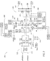
- FIG. 2 illustrates an example power supply having a primary side 202 and a secondary side 204.
- the amplifier system 200 may include the converter 130 and/or the class D amplifier 135.
- the system 200 may be a single half bridge amplifier having a half-bridge converter 211.
- the amplifier 135 may include various drivers, including a first driver 206 and a second driver 208 on the secondary side 204.
- a booster 210 may be arranged on the primary side 202 at the converter 211 configured to receive the DC power supply.
- the system 200 may also include a flyback converter 212.
- the voltage rails 140, 142 may each include a pair of diodes.
- the first voltage rail 140 also referred to herein as a first side and positive side, may include a first diode 216 and a second diode 218.
- the second voltage rail 142 also referred to herein as a second side and negative side, may include a third diode 220 and a fourth diode 222.
- a pair of metal-oxide-semiconductor field-effect transistors (MOSFETS) may be associated with each voltage rail 140, 142.
- a first MOSFET 230 may be arranged parallel with the first diode 216, a second MOSFET 232 may be arranged parallel with the second diode 218, a third MOSFET 234 may be arranged in parallel with the third diode 220, and a fourth MOSFET 236 may be arranged in parallel with the fourth diode 222.
- a pair of bootstrap diodes including a first bootstrap diode 238, also referred to as first ground diode 238, and a second bootstrap diode 240, also referred to as second first ground diode 238, may be arranged at each of the converters 211, 212.
- a pair of capacitors including a first capacitor 242 and a second capacitor 244 may also be arranged at each of the converters 211, 212.
- the capacitors may be configured to store energy.
- the capacitors 242, 244, as explained herein, may store energy alternatively to one another, that is as one charges, the other discharges.
- a loaded converter output is the side of the power supply that supplies a first supply voltage to the respective rail from which the class D amplifier is currently drawing power.
- An unloaded converter is the portion that supplies a second supply voltage to the second rail and is not intended to be currently drawing power. That is, when power is supplied on the first rail 140, that side of the transformer is loaded and the opposite side associated with the second rail 142 is unloaded. The converse is true in that when the second rail 142 is powered the associated side of the transformer is loaded with the side of the transformer associated with the first rail 140 is unloaded.
- Off-side charging, or rail pumping occurs in class D amplifiers as the load of the amplifier is coupled between the loaded converter output. Rail pumping will cause the boosting beyond rated or intended magnitude levels on the unloaded rail.
- the system 200 may carefully operate the MOSFETs and diodes to not block reverse current, allowing current to flow through the opposite transformer side.
- a first set of components will be active while a second set of components is not, and the second set will be active while the first set is not.
- the first set may include the first and fourth MOSFET/diode pairs, as well as the second bootstrap diode 240.
- the first set may operate simultaneously.
- the first MOSFET 230, the first diode 216, fourth MOSFET 236, fourth diode 222, and second bootstrap diode 240 may all be active simultaneously.
- the second and third MOSFET/diode pairs will operate simultaneously with one another.
- the second MOSFET 232, the second diode 218, third MOSFET 234, third diode 220, and first ground diode 238 may all be active simultaneously, but the first or fourth MOSFET/diodes will not be.
- the first capacitor 242 When the first set of components is active, the first capacitor 242 may store energy as current is passed therethrough. The second capacitor 244 may discharge. When the second set of components are active, the second capacitor 244 may charge, while the first capacitor 242 is discharged. This may be possible due to current being permitted to flow through the respective capacitors and not be blocked by commonly used diode rectifiers.
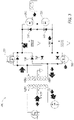
- FIGs. 3 and 4 each illustrate and example schematic of another system 300 having a primary side 302 and a secondary side 304.
- FIG. 3 illustrates current flow for operating during a positive portion of the cycle.
- FIG. 4 illustrates current flow for operating during a negative portion of the cycle.
- This system 300 may be similar to FIG. 2 in that various MOSFET and diodes are controlled to mitigate rail pumping.
- the system 300 includes half bride converter 311.
- the system 300 may include a first diode 316, a second diode 318, a third diode 320, and a fourth diode 322.
- a first MOSFET 330 may be arranged parallel with the first diode 216
- a second MOSFET 332 may be arranged parallel with the second diode 318
- a third MOSFET 334 may be arranged in parallel with the third diode 320
- a fourth MOSFET 336 may be arranged in parallel with the fourth diode 322.
- certain components may operate simultaneously in order to allow reverse current from flowing through the opposite, unloaded side creating a synchronous rectification through the system 200.
- Such rectification aids in decreasing the pumping or boosting on the voltage rails 140, 142 and thus diminishes the affects of any rail pumping.
- the first MOSFET 330, the first diode 316, fourth MOSFET 336, and fourth diode 322 may all be active simultaneously when operating in the positive portion.
- the inductor current is consistently outward in this state. Any traditional rail pumping current travels via the third and fourth MOSFETS 334, 336.
- the first arrows 350 indicate the loaded side current flow while the second arrows 352 indicate the unloaded side current flow.
- inductor current when operating during the negative portion as the loaded side, inductor current is consistently inward.
- the second MOSFET 332, the second diode 318, third MOSFET 334, and third diode 320 may all be active simultaneously. Because the inductor current in consistently inward in this state, the rail pumping current travels via the first and second MOSFETS 330, 332. This allows currently flow back on the unloaded side, while allowing the second capacitor 344 to be charged while the first capacitor 342 is discharged. Because reverse current is permitted on the unloaded side, the power supply is able to recirculate this current to the opposite unloaded rail, clamping the effects of rail pumping.
- FIG. 5 illustrates a series of waveforms referenced in FIG. 2 .
- the waveforms may represent certain signals indicated on FIG. 2 .
- Various driver inputs may be illustrated, for example, a first driver ePWM2A, first driver ePWM4B, second driver ePWM2B and second driver ePWM4B.
- an amplifier system that uses MOSFETS to allow recirculating current to the opposing voltage rail to mitigate rail pumping.
- MOSFETS to allow recirculating current to the opposing voltage rail to mitigate rail pumping.
- the power supply is able to recirculate current to the unloaded voltage rail instead of blocking the current with traditional diode rectifiers.
- aspects of the present embodiments may be embodied as a system, method or computer program product. Accordingly, aspects of the present disclosure may take the form of an entirely hardware embodiment, an entirely software embodiment (including firmware, resident software, micro-code, etc.) or an embodiment combining software and hardware aspects that may all generally be referred to herein as a "module” or "system.” Furthermore, aspects of the present disclosure may take the form of a computer program product embodied in one or more computer readable medium(s) having computer readable program code embodied thereon.
- the computer readable medium may be a computer readable signal medium or a computer readable storage medium.
- a computer readable storage medium may be, for example, but not limited to, an electronic, magnetic, optical, electromagnetic, infrared, or semiconductor system, apparatus, or device, or any suitable combination of the foregoing.
- the computer readable storage medium includes the following: an electrical connection having one or more wires, a portable computer diskette, a hard disk, a random access memory (RAM), a read-only memory (ROM), an erasable programmable read-only memory (erasable programmable read-only memory (EPROM) or Flash memory), an optical fiber, a portable compact disc read-only memory (CD-ROM), an optical storage device, a magnetic storage device, or any suitable combination of the foregoing.
- a computer readable storage medium may be any tangible medium that can contain, or store a program for use by or in connection with an instruction execution system, apparatus, or device.
- each block in the flowchart or block diagrams may represent a module, segment, or portion of code, which comprises one or more executable instructions for implementing the specified logical function(s).
- the functions noted in the block may occur out of the order noted in the figures. For example, two blocks shown in succession may, in fact, be executed substantially concurrently, or the blocks may sometimes be executed in the reverse order, depending upon the functionality involved.
Landscapes
- Engineering & Computer Science (AREA)
- Power Engineering (AREA)
- Microelectronics & Electronic Packaging (AREA)
- Multimedia (AREA)
- Dc-Dc Converters (AREA)
Applications Claiming Priority (1)
| Application Number | Priority Date | Filing Date | Title |
|---|---|---|---|
| US17/240,268 US11777415B2 (en) | 2021-04-26 | 2021-04-26 | Synchronous rectification to mitigate rail pumping in a single-ended Class D amplifier |
Publications (1)
| Publication Number | Publication Date |
|---|---|
| EP4084331A1 true EP4084331A1 (de) | 2022-11-02 |
Family
ID=81387312
Family Applications (1)
| Application Number | Title | Priority Date | Filing Date |
|---|---|---|---|
| EP22170032.1A Withdrawn EP4084331A1 (de) | 2021-04-26 | 2022-04-26 | Synchrone gleichrichtung zum abschwächen des rail-pumpens in einem unsymmetrischen class-d-verstärker |
Country Status (3)
| Country | Link |
|---|---|
| US (1) | US11777415B2 (de) |
| EP (1) | EP4084331A1 (de) |
| CN (1) | CN115250077A (de) |
Citations (3)
| Publication number | Priority date | Publication date | Assignee | Title |
|---|---|---|---|---|
| WO2007096761A1 (en) * | 2006-02-24 | 2007-08-30 | Bang & Olufsen Icepower A/S | Audio power conversion system |
| US20090309658A1 (en) * | 2008-06-16 | 2009-12-17 | Rgb Systems, Inc. | Method and apparatus for power converter for class d audio power amplifiers |
| US20180123534A1 (en) * | 2016-10-31 | 2018-05-03 | Rgb Systems, Inc. | Power supply for class d amplifier in energy efficient applications |
Family Cites Families (1)
| Publication number | Priority date | Publication date | Assignee | Title |
|---|---|---|---|---|
| US10014831B1 (en) * | 2017-02-23 | 2018-07-03 | Crestron Electronics, Inc. | Audio amplifier power supply rail-balancing and anti-pumping system |
-
2021
- 2021-04-26 US US17/240,268 patent/US11777415B2/en active Active
-
2022
- 2022-04-25 CN CN202210441057.XA patent/CN115250077A/zh active Pending
- 2022-04-26 EP EP22170032.1A patent/EP4084331A1/de not_active Withdrawn
Patent Citations (5)
| Publication number | Priority date | Publication date | Assignee | Title |
|---|---|---|---|---|
| WO2007096761A1 (en) * | 2006-02-24 | 2007-08-30 | Bang & Olufsen Icepower A/S | Audio power conversion system |
| EP1987585A1 (de) * | 2006-02-24 | 2008-11-05 | Bang & Olufsen IcePower A/S | Audioleistungsumsetzungssystem |
| EP1987585B1 (de) * | 2006-02-24 | 2011-08-17 | Bang & Olufsen IcePower A/S | Audioleistungsumsetzungssystem |
| US20090309658A1 (en) * | 2008-06-16 | 2009-12-17 | Rgb Systems, Inc. | Method and apparatus for power converter for class d audio power amplifiers |
| US20180123534A1 (en) * | 2016-10-31 | 2018-05-03 | Rgb Systems, Inc. | Power supply for class d amplifier in energy efficient applications |
Non-Patent Citations (3)
| Title |
|---|
| HUANG RUI ET AL: "Embedded Bidirectional Buck-Boost Converter in Half Bridge Class-D Audio Amplifier for Suppressing Bus Voltage Pumping", IEEE TRANSACTIONS ON INDUSTRIAL ELECTRONICS, IEEE SERVICE CENTER, PISCATAWAY, NJ, USA, vol. 69, no. 2, 9 February 2021 (2021-02-09), pages 1454 - 1464, XP011885706, ISSN: 0278-0046, [retrieved on 20211028], DOI: 10.1109/TIE.2021.3056997 * |
| XU DUO ET AL: "Front-End Bidirectional Symmetric Bipolar Outputs LLC DC-Transformer (DCX) for a Half Bridge Class-D Audio Amplifier", IEEE TRANSACTIONS ON INDUSTRIAL ELECTRONICS, IEEE SERVICE CENTER, PISCATAWAY, NJ, USA, vol. 68, no. 11, 19 November 2020 (2020-11-19), pages 10750 - 10760, XP011868356, ISSN: 0278-0046, [retrieved on 20210729], DOI: 10.1109/TIE.2020.3038071 * |
| ZHOU XIANG ET AL: "An Electrolytic Capacitor-Free Half Bridge Class-D Audio Amplifier System Without Bus-Voltage Pumping", IEEE TRANSACTIONS ON POWER ELECTRONICS, INSTITUTE OF ELECTRICAL AND ELECTRONICS ENGINEERS, USA, vol. 36, no. 8, 6 January 2021 (2021-01-06), pages 9221 - 9236, XP011854056, ISSN: 0885-8993, [retrieved on 20210511], DOI: 10.1109/TPEL.2021.3049596 * |
Also Published As
| Publication number | Publication date |
|---|---|
| CN115250077A (zh) | 2022-10-28 |
| US11777415B2 (en) | 2023-10-03 |
| US20220345047A1 (en) | 2022-10-27 |
Similar Documents
| Publication | Publication Date | Title |
|---|---|---|
| US9641133B2 (en) | Adaptive rail power amplifier technology | |
| US20140354246A1 (en) | Bridgeless pfc power converter with high efficiency | |
| US11171557B2 (en) | Power converter | |
| US20150002108A1 (en) | Bridgeless power factor correction boost converter | |
| US9906169B1 (en) | DC-AC conversion circuit having a first double ended DC pulse stage and a second AC stage | |
| US20130258721A1 (en) | Control device employed in a switched electrical power supply system | |
| JP2013169057A (ja) | スイッチング電源回路 | |
| US20130241290A1 (en) | Filter circuit and bidirectional power conversion apparatus including thereof | |
| US10673318B2 (en) | Converter apparatus and method with auxiliary transistor for protecting components at startup | |
| US12101020B2 (en) | Multi-mode power system and power conversion circuit thereof | |
| Kim et al. | Voltage doubler rectified boost-integrated half bridge (VDRBHB) converter for digital car audio amplifiers | |
| WO2023243321A1 (ja) | コンバータ装置 | |
| JPWO2018198893A1 (ja) | 電力変換システム | |
| Zhang et al. | Investigation of adaptive synchronous rectifier (SR) driving scheme for LLC/CLLC resonant converter in EV on-board chargers | |
| WO2019177685A1 (en) | Coupled-inductor cascaded buck convertor with fast transient response | |
| EP4084331A1 (de) | Synchrone gleichrichtung zum abschwächen des rail-pumpens in einem unsymmetrischen class-d-verstärker | |
| US11205969B2 (en) | Inverter device configured to operate in a CCM and sequentially operate in buck and boost phases | |
| US20230402977A1 (en) | System and method for reduction in power supply rail pumping in class d audio amplifiers using dual regulated dc-dc converters | |
| WO2023127464A1 (ja) | 電力変換システム | |
| KR20200124057A (ko) | 모터 제어 장치 | |
| WO2022168635A1 (ja) | 電力変換システム及び制御方法 | |
| JP7039430B2 (ja) | Ac/dcコンバータ | |
| US11522463B2 (en) | System and method to extend low line operation of flyback converters | |
| US12249903B2 (en) | Switching technique using PWM for increasing switching efficiency | |
| US9018926B1 (en) | Soft-switched PFC converter |
Legal Events
| Date | Code | Title | Description |
|---|---|---|---|
| PUAI | Public reference made under article 153(3) epc to a published international application that has entered the european phase |
Free format text: ORIGINAL CODE: 0009012 |
|
| STAA | Information on the status of an ep patent application or granted ep patent |
Free format text: STATUS: THE APPLICATION HAS BEEN PUBLISHED |
|
| AK | Designated contracting states |
Kind code of ref document: A1 Designated state(s): AL AT BE BG CH CY CZ DE DK EE ES FI FR GB GR HR HU IE IS IT LI LT LU LV MC MK MT NL NO PL PT RO RS SE SI SK SM TR |
|
| STAA | Information on the status of an ep patent application or granted ep patent |
Free format text: STATUS: REQUEST FOR EXAMINATION WAS MADE |
|
| 17P | Request for examination filed |
Effective date: 20230502 |
|
| RBV | Designated contracting states (corrected) |
Designated state(s): AL AT BE BG CH CY CZ DE DK EE ES FI FR GB GR HR HU IE IS IT LI LT LU LV MC MK MT NL NO PL PT RO RS SE SI SK SM TR |
|
| GRAP | Despatch of communication of intention to grant a patent |
Free format text: ORIGINAL CODE: EPIDOSNIGR1 |
|
| STAA | Information on the status of an ep patent application or granted ep patent |
Free format text: STATUS: GRANT OF PATENT IS INTENDED |
|
| INTG | Intention to grant announced |
Effective date: 20250404 |
|
| STAA | Information on the status of an ep patent application or granted ep patent |
Free format text: STATUS: THE APPLICATION IS DEEMED TO BE WITHDRAWN |
|
| 18D | Application deemed to be withdrawn |
Effective date: 20250805 |