EP4083706B1 - Verfahren zur strukturierung einer hybriden oberfläche durch plasmaätzen - Google Patents
Verfahren zur strukturierung einer hybriden oberfläche durch plasmaätzen Download PDFInfo
- Publication number
- EP4083706B1 EP4083706B1 EP22170196.4A EP22170196A EP4083706B1 EP 4083706 B1 EP4083706 B1 EP 4083706B1 EP 22170196 A EP22170196 A EP 22170196A EP 4083706 B1 EP4083706 B1 EP 4083706B1
- Authority
- EP
- European Patent Office
- Prior art keywords
- patterns
- resin
- roughness
- sio
- comprised
- Prior art date
- Legal status (The legal status is an assumption and is not a legal conclusion. Google has not performed a legal analysis and makes no representation as to the accuracy of the status listed.)
- Active
Links
Images

Classifications
-
- G—PHYSICS
- G03—PHOTOGRAPHY; CINEMATOGRAPHY; ANALOGOUS TECHNIQUES USING WAVES OTHER THAN OPTICAL WAVES; ELECTROGRAPHY; HOLOGRAPHY
- G03F—PHOTOMECHANICAL PRODUCTION OF TEXTURED OR PATTERNED SURFACES, e.g. FOR PRINTING, FOR PROCESSING OF SEMICONDUCTOR DEVICES; MATERIALS THEREFOR; ORIGINALS THEREFOR; APPARATUS SPECIALLY ADAPTED THEREFOR
- G03F7/00—Photomechanical, e.g. photolithographic, production of textured or patterned surfaces, e.g. printing surfaces; Materials therefor, e.g. comprising photoresists; Apparatus specially adapted therefor
- G03F7/26—Processing photosensitive materials; Apparatus therefor
- G03F7/40—Treatment after imagewise removal, e.g. baking
-
- G—PHYSICS
- G03—PHOTOGRAPHY; CINEMATOGRAPHY; ANALOGOUS TECHNIQUES USING WAVES OTHER THAN OPTICAL WAVES; ELECTROGRAPHY; HOLOGRAPHY
- G03F—PHOTOMECHANICAL PRODUCTION OF TEXTURED OR PATTERNED SURFACES, e.g. FOR PRINTING, FOR PROCESSING OF SEMICONDUCTOR DEVICES; MATERIALS THEREFOR; ORIGINALS THEREFOR; APPARATUS SPECIALLY ADAPTED THEREFOR
- G03F7/00—Photomechanical, e.g. photolithographic, production of textured or patterned surfaces, e.g. printing surfaces; Materials therefor, e.g. comprising photoresists; Apparatus specially adapted therefor
- G03F7/0002—Lithographic processes using patterning methods other than those involving the exposure to radiation, e.g. by stamping
-
- G—PHYSICS
- G03—PHOTOGRAPHY; CINEMATOGRAPHY; ANALOGOUS TECHNIQUES USING WAVES OTHER THAN OPTICAL WAVES; ELECTROGRAPHY; HOLOGRAPHY
- G03F—PHOTOMECHANICAL PRODUCTION OF TEXTURED OR PATTERNED SURFACES, e.g. FOR PRINTING, FOR PROCESSING OF SEMICONDUCTOR DEVICES; MATERIALS THEREFOR; ORIGINALS THEREFOR; APPARATUS SPECIALLY ADAPTED THEREFOR
- G03F7/00—Photomechanical, e.g. photolithographic, production of textured or patterned surfaces, e.g. printing surfaces; Materials therefor, e.g. comprising photoresists; Apparatus specially adapted therefor
- G03F7/004—Photosensitive materials
- G03F7/027—Non-macromolecular photopolymerisable compounds having carbon-to-carbon double bonds, e.g. ethylenic compounds
-
- G—PHYSICS
- G03—PHOTOGRAPHY; CINEMATOGRAPHY; ANALOGOUS TECHNIQUES USING WAVES OTHER THAN OPTICAL WAVES; ELECTROGRAPHY; HOLOGRAPHY
- G03F—PHOTOMECHANICAL PRODUCTION OF TEXTURED OR PATTERNED SURFACES, e.g. FOR PRINTING, FOR PROCESSING OF SEMICONDUCTOR DEVICES; MATERIALS THEREFOR; ORIGINALS THEREFOR; APPARATUS SPECIALLY ADAPTED THEREFOR
- G03F7/00—Photomechanical, e.g. photolithographic, production of textured or patterned surfaces, e.g. printing surfaces; Materials therefor, e.g. comprising photoresists; Apparatus specially adapted therefor
- G03F7/004—Photosensitive materials
- G03F7/075—Silicon-containing compounds
- G03F7/0755—Non-macromolecular compounds containing Si-O, Si-C or Si-N bonds
-
- G—PHYSICS
- G03—PHOTOGRAPHY; CINEMATOGRAPHY; ANALOGOUS TECHNIQUES USING WAVES OTHER THAN OPTICAL WAVES; ELECTROGRAPHY; HOLOGRAPHY
- G03F—PHOTOMECHANICAL PRODUCTION OF TEXTURED OR PATTERNED SURFACES, e.g. FOR PRINTING, FOR PROCESSING OF SEMICONDUCTOR DEVICES; MATERIALS THEREFOR; ORIGINALS THEREFOR; APPARATUS SPECIALLY ADAPTED THEREFOR
- G03F7/00—Photomechanical, e.g. photolithographic, production of textured or patterned surfaces, e.g. printing surfaces; Materials therefor, e.g. comprising photoresists; Apparatus specially adapted therefor
- G03F7/20—Exposure; Apparatus therefor
- G03F7/2051—Exposure without an original mask, e.g. using a programmed deflection of a point source, by scanning, by drawing with a light beam, using an addressed light or corpuscular source
- G03F7/2059—Exposure without an original mask, e.g. using a programmed deflection of a point source, by scanning, by drawing with a light beam, using an addressed light or corpuscular source using a scanning corpuscular radiation beam, e.g. an electron beam
-
- G—PHYSICS
- G03—PHOTOGRAPHY; CINEMATOGRAPHY; ANALOGOUS TECHNIQUES USING WAVES OTHER THAN OPTICAL WAVES; ELECTROGRAPHY; HOLOGRAPHY
- G03F—PHOTOMECHANICAL PRODUCTION OF TEXTURED OR PATTERNED SURFACES, e.g. FOR PRINTING, FOR PROCESSING OF SEMICONDUCTOR DEVICES; MATERIALS THEREFOR; ORIGINALS THEREFOR; APPARATUS SPECIALLY ADAPTED THEREFOR
- G03F7/00—Photomechanical, e.g. photolithographic, production of textured or patterned surfaces, e.g. printing surfaces; Materials therefor, e.g. comprising photoresists; Apparatus specially adapted therefor
- G03F7/70—Microphotolithographic exposure; Apparatus therefor
- G03F7/70008—Production of exposure light, i.e. light sources
- G03F7/70025—Production of exposure light, i.e. light sources by lasers
Definitions
- the invention relates to structuring techniques, making it possible to produce a hybrid structure, comprising for example patterns on a micrometric scale and an etching of at least part of these patterns in order to give them a roughness on a nanometric scale.
- This type of hybrid structure makes it possible in particular to create a surface which has antibacterial and antiviral properties, with a controlled rough texturing on at least part of the surface of the patterns.
- Antibacterial surfaces are typically created either by plasma deposition with Si-rich precursors (by plasma "HMDSO”) (see the article by Zouaghi et al. 2018, Applied Surface Science, Volume 455, 15 October 2018, Pages 392-402: “Atmospheric pressure plasma spraying of silane-based coatings targeting whey protein fouling and bacterial adhesion management »), or by laser ablation of a metal surface ( S. Moradi et al.; ACS Appl. Mater.
- the invention firstly relates to a method for producing a hybrid structure, comprising the steps defined in claim 1.
- the polymerization of the resin may take place between the steps of forming a structure comprising a plurality of patterns and forming a roughness on at least a portion of the surface of the patterns, as defined in claim 1.
- Each pattern has at least one dimension, measured parallel or perpendicular to the substrate, between 50 nm and 500 ⁇ m, for example 100 nm or 1 ⁇ m.
- the patterns can be said to be “micrometric”.
- the patterns can be made in the mineral resin layer, for example by an optical or electronic lithography process or even by a nano-printing technique.
- the patterns for example micrometric, can have either a crenel shape, a cone shape, a pyramid shape or other. These patterns make it possible to obtain a dewetting surface on which bacteria do not adhere, which can be further reinforced by grafting.
- the roughness (corresponding to a nanometric structuring with a critical dimension for example less than 50 nm) can be obtained for example by an oxidizing process, of the type comprising at least one species or a gas making it possible to consume more or less the mineral phase of the resin, and thus to reveal areas having vacancies in atoms or molecules of Si and/or SiO 2 .
- These atoms or molecules of Si and/or SiO 2 are not consumed by this oxidizing process (the atoms of Si can nevertheless be oxidized into SiO 2 ).
- This oxidizing process is for example an etching by plasma, isotropic or anisotropic.
- the surface thus created is rich in Si and/or SiO 2 , which allows, in addition to the surface texture thus obtained, which is favorable to antibacterial and antiviral applications, to graft silanes thereon, for example to change the surface energy properties in order to increase the dewetting effect.
- the silanes therefore help with dewetting, and therefore advantageously complete the patterns or microstructures.
- a mineral resin containing a proportion of Si and/or SiO 2 (denoted Si/SiO 2 hereinafter) of between 1% and 30% (in molar mass) is chosen.
- a resin comprising a higher proportion of Si/SiO 2 can be treated to reduce it by adding an organic compound, such as another resin or a precursor.
- an implantation of Si is possible to increase it.
- the chosen resin in particular its Si/ SiO2 proportion of between 1% and 30%, is compatible with at least one optical or electronic lithography process or an alternative technique (such as nano-imprinting) to produce a first level of structures.
- a qualification process can be carried out with respect to each technique as for example described in the article by Kretz et al. “Comparative study of calixarene and HSQ resist systems for the fabrication of sub-20 nm MOSFET device demonstrators”, published in Microelectronic Engineering, 78-79, 2005, 479-483 .
- Nanoimprint can also easily produce protruding shapes (cone or pyramid in particular) which will allow bacteria to be denatured.
- the quantity of resin to be used is defined as well as the spreading, exposure, development parameters and the parameters of any intermediate annealing.
- the resin of this example contains 4% silicon, which is in the adequate range 1%-30% to implement a process according to the invention.
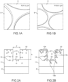
- each pattern has at least one of its dimensions measured parallel (l) or perpendicular (h) to the substrate, between 50 nm and 1 mm.
- l can in particular be the width of the opening of the cavity, measured between the side walls 21 thereof;
- h can be the depth of this cavity, measured between the upper surface 22 of the pattern and its lower surface (or its bottom or its lower part) 23.
- the parameters used for the resin shaping process are as follows (with “EVG Hercules cluster” type equipment): 500 mbar (pressure corresponding to the force relief applied to the flexible mold), lamp power of 600 mW/ cm2 (this power can be adjusted, for example between 50 and 600 mW/ cm2 ), for an exposure time of 8s, for an initial resin thickness of 800 nm.
- Any other shape of pattern can be made, for example cone-shaped or pyramid-shaped patterns or other.
- the process used is then adapted to the desired shape; for example, the shape of the mold is adapted to the desired pattern shape.
- an oxidizing process comprising at least one species or gas allowing the consumption slightly the mineral phase to reveal areas with vacancies in Si/SiO 2 compounds.
- this gas can be composed of a fluorinated element (CF 4 , SF 6 ) and the Oxygen/Fluorine ratio can be modified in order to vary the roughness.
- Figure 2B represents the pattern of the Figure 2A , produced in mineral resin 11, after implementation of the oxidizing process: the references 13a, 13b, 13c designate the roughness obtained (these are of course schematic representations), both on the upper parts 22 of the patterns, and on the sides 21 or on the bottom 23.
- a resin with too high a Si/SiO 2 content does not allow the desired roughness to be obtained (for example SiArc with 40 - 50%, also referred to as JSR ISX412).
- a resin with too high a Si/SiO 2 content does not allow the desired roughness to be obtained (for example SiArc with 40 - 50%, also referred to as JSR ISX412).
- an ISX412 resin and the precursor IRGACURE 4265 from BASF are used.
- this material is non-printable; it becomes so with a proportion of 5 to 15% added agent, for printing times between 20 minutes (at 5% IRGACURE) and 5 minutes (at 15% IRGACURE), under a pressure of 30 bar and at 100°C.
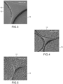
- An etch-back step is applied to resurface the upper portions 22 of the printed patterns, as illustrated in figure 7 ; but the roughness is not revealed (because the proportion of SiO 2 is too high, greater than 30%), and it is not revealed either by extending the etching (under O 2 /HBr plasma, with a bias of 500 W) as presented on the figure 8 .
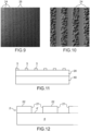
- the roughness of the upper part of the patterns 24 is revealed from the etch-back stage ( figure 9 ) (because the proportion of Si/SiO2 is in the range 1-30%), and it is possible to completely remove the organic part 26 simply by extending the etching time ( figure 10 ; also under O2 /HBr plasma with 500 W bias).
- the resin layer 2 is deposited on a substrate 4 (see Figure 2A ) in silicon.
- the resin on a layer 40 (see figure 11 ) of negative resin, after crosslinking or polymerization of the latter.
- a layer 40 see figure 11
- micrometric patterns by nano-imprinting in layer 2: this technique makes it possible to keep resin at the bottom of the patterns, as in Figure 2A .
- the micrometric patterns can be produced by optical or electronic lithography, using a mask 3, as shown in figure 11 .
- the background of the patterns is formed by the upper surface 4' of the underlying substrate but not by the resin in which the patterns are made.
- the figure 12 represents micrometric patterns produced in a layer 2 of resin, by optical or electronic lithography, on a silicon support substrate 4, the upper surface 4' of which constitutes the background of the patterns.
- the roughness can be formed only on the upper parts 22 of the patterns ( figure 12 ), or both on the upper parts 22 and the side parts 21.
- the roughening can be carried out only on the upper part 22 and lower part 23 of the micrometric patterns, or also on the lateral parts 21, using an anisotropic plasma.
- a structured surface obtained by a process according to the invention allows the grafting of fluorinated agents (which help with dewetting and therefore the evacuation of “dead” bacteria more easily in a solvent such as water) or silane.
- the grafting takes place on the nanometric patterns.
- the patterns can have various shapes, for example circular, as illustrated in the Figures 1A-1B , 7, 8 or in the form of parallel strips between them, as illustrated in figures 9, 10 .
- a property of a structured surface obtained by a method according to the invention is that viruses cannot adhere to it due to the microstructures and the grafting carried out on the surface; the viruses are furthermore damaged by the roughness (nanometric structure) and where appropriate by the microstructure when the latter is of a protruding shape.
Landscapes
- Physics & Mathematics (AREA)
- General Physics & Mathematics (AREA)
- Spectroscopy & Molecular Physics (AREA)
- Engineering & Computer Science (AREA)
- Optics & Photonics (AREA)
- Plasma & Fusion (AREA)
- Health & Medical Sciences (AREA)
- Toxicology (AREA)
- Treatments Of Macromolecular Shaped Articles (AREA)
- Shaping Of Tube Ends By Bending Or Straightening (AREA)
- Laminated Bodies (AREA)
Claims (10)
- Verfahren zum Herstellen einer hybriden Struktur, das Folgendes umfasst:- Bilden einer Schicht (2) aus Mineralharz, die einen Anteil von Si und/oder SiO2 umfasst, der zwischen 1 % und 30 % der Molmasse liegt, auf einem Substrat (4, 40);- Bilden einer Struktur, die eine Vielzahl von Mustern (6) in der Schicht umfasst, die mindestens eine parallel oder senkrecht zum Substrat gemessene Abmessung (h, l) aufweist, die zwischen 50 nm und 500 µm liegt;- Bilden einer Rauheit (Ra) auf mindestens einem Teil der Oberfläche der Muster durch ein Oxidationsverfahren, das mindestens eine Spezies oder ein Gas umfasst, das einen Teil der Mineralphase verbraucht.
- Verfahren nach Anspruch 1, wobei das Oxidationsverfahren ein fluorhaltiges Element verwendet.
- Verfahren nach Anspruch 2, wobei das Oxidationsverfahren SF6 und/oder CF4 verwendet.
- Verfahren nach Anspruch 3, wobei das Oxidationsverfahren SF6 mit einem Verhältnis von SF6/O2 zwischen 1:25 und 3:25 verwendet.
- Verfahren nach einem der Ansprüche 1 bis 4, wobei die Rauheit der Muster durch isotropes oder anisotropes Plasmaätzen erhalten wird.
- Verfahren nach einem der Ansprüche 1 bis 5, wobei das Substrat (4, 40) aus Silizium oder einem vernetzten Negativharz besteht.
- Verfahren nach einem der Ansprüche 1 bis 6, wobei die Vielzahl von Mustern in der Harzschicht (2) durch Nanoprägung oder durch optische Lithografie oder Elektronenstrahllithografie erhalten werden.
- Verfahren nach einem der Ansprüche 1 bis 7, wobei die erhaltene durchschnittliche Rauheit (Ra) auf mindestens einem Teil der Muster zwischen 0,5 nm und 30 nm liegt.
- Verfahren nach einem der Ansprüche 1 bis 8, wobei benachbarte Muster (6) durch einen Abstand, der zwischen 50 nm und 1 mm liegt, getrennt sind.
- Verfahren nach einem der Ansprüche 1 bis 9, das ferner einen Schritt des Aufpfropfens von mindestens einem fluorhaltigen Mittel oder Silan umfasst.
Applications Claiming Priority (1)
| Application Number | Priority Date | Filing Date | Title |
|---|---|---|---|
| FR2104582A FR3122523B1 (fr) | 2021-04-30 | 2021-04-30 | Procede de structuration de surface hybride par gravure plasma |
Publications (2)
| Publication Number | Publication Date |
|---|---|
| EP4083706A1 EP4083706A1 (de) | 2022-11-02 |
| EP4083706B1 true EP4083706B1 (de) | 2025-02-19 |
Family
ID=76807763
Family Applications (1)
| Application Number | Title | Priority Date | Filing Date |
|---|---|---|---|
| EP22170196.4A Active EP4083706B1 (de) | 2021-04-30 | 2022-04-27 | Verfahren zur strukturierung einer hybriden oberfläche durch plasmaätzen |
Country Status (3)
| Country | Link |
|---|---|
| US (1) | US20220350252A1 (de) |
| EP (1) | EP4083706B1 (de) |
| FR (1) | FR3122523B1 (de) |
Family Cites Families (7)
| Publication number | Priority date | Publication date | Assignee | Title |
|---|---|---|---|---|
| KR101171190B1 (ko) * | 2005-11-02 | 2012-08-06 | 삼성전자주식회사 | 표시장치의 제조방법과 이에 사용되는 몰드 |
| CN101849281B (zh) * | 2007-08-28 | 2013-09-18 | 科技研究局 | 一种制造有机电子器件或者光电器件的方法 |
| EP2252545A2 (de) * | 2008-03-10 | 2010-11-24 | Yeda Research And Development Company Ltd. | Verfahren zur herstellung nanoskaliger strukturierter oberflächen |
| FR2990384B1 (fr) * | 2012-05-14 | 2015-05-15 | Saint Gobain | Procede de texturation sur un substrat de grande surface |
| US20180028029A1 (en) * | 2016-06-03 | 2018-02-01 | Atieh Haghdoost | Drying apparatus comprising a hydrophobic material |
| EP3533090A1 (de) * | 2016-10-28 | 2019-09-04 | 3M Innovative Properties Company | Nanostrukturierter artikel |
| TWI741262B (zh) * | 2018-06-04 | 2021-10-01 | 美商帕斯馬舍門有限責任公司 | 切割晶粒附接膜的方法 |
-
2021
- 2021-04-30 FR FR2104582A patent/FR3122523B1/fr not_active Expired - Fee Related
-
2022
- 2022-04-21 US US17/660,099 patent/US20220350252A1/en not_active Abandoned
- 2022-04-27 EP EP22170196.4A patent/EP4083706B1/de active Active
Also Published As
| Publication number | Publication date |
|---|---|
| US20220350252A1 (en) | 2022-11-03 |
| FR3122523B1 (fr) | 2023-06-09 |
| EP4083706A1 (de) | 2022-11-02 |
| FR3122523A1 (fr) | 2022-11-04 |
Similar Documents
| Publication | Publication Date | Title |
|---|---|---|
| EP2715782B1 (de) | Verfahren zur herstellung von mustern auf der oberfläche eines substrats unter verwendung von block-copolymeren | |
| Schift et al. | Fabrication of polymer photonic crystals using nanoimprint lithography | |
| EP3238233B1 (de) | Verfahren zur erzeugung von mustern | |
| WO2015075380A1 (fr) | Procédé de gravure sélective d'un masque disposé sur un substrat silicié | |
| FR2926162A1 (fr) | Procede de modification localisee de l'energie de surface d'un substrat | |
| EP3249468B1 (de) | Verfahren zur herstellung von motiven | |
| EP2769249A1 (de) | Verfahren zur herstellung einer refraktiven oder diffraktiven optischen vorrichtung | |
| US8821743B2 (en) | Manufacturing method of grating | |
| US20150087153A1 (en) | Method of manufacturing howllow-structure metal grating | |
| EP3238231B1 (de) | Verfahren zur erzeugung von mustern in einer schicht | |
| EP4083706B1 (de) | Verfahren zur strukturierung einer hybriden oberfläche durch plasmaätzen | |
| JP2017063099A (ja) | 凹凸構造を含む基板の製造方法及び半導体発光素子の製造方法 | |
| EP3465739B1 (de) | Verfahren zur herstellung eines funktionalisierten führungsmusters für ein graphoepitaxieverfahren | |
| EP1576420B1 (de) | Lithografieverfahren durch pressen eines substrats in einem nanoimprint-prozess | |
| EP3347768A1 (de) | Verfahren zum selektiven ätzen eines blockcopolymers | |
| FR3066857B1 (fr) | Procede de realisation de motifs dans un substrat | |
| EP3465741A1 (de) | Verfahren zur gerichteten selbstanordnung eines blockcopolymers durch graphoepitaxie | |
| EP4102579A1 (de) | Verfahren zur herstellung eines substrats mit einer relaxierten inganschicht und so erhaltenes substrat für die wiederaufnahme des wachstums einer led-struktur | |
| EP3358631B1 (de) | Bildung von reliefs auf der oberfläche eines substrats | |
| WO2020048955A1 (fr) | Procédé de gravure d'un copolymère à blocs comprenant une étape de dépôt sélectif | |
| CH710482A2 (fr) | Procédé de gravure chimique du dioxyde de silicium. |
Legal Events
| Date | Code | Title | Description |
|---|---|---|---|
| PUAI | Public reference made under article 153(3) epc to a published international application that has entered the european phase |
Free format text: ORIGINAL CODE: 0009012 |
|
| STAA | Information on the status of an ep patent application or granted ep patent |
Free format text: STATUS: REQUEST FOR EXAMINATION WAS MADE |
|
| 17P | Request for examination filed |
Effective date: 20220427 |
|
| AK | Designated contracting states |
Kind code of ref document: A1 Designated state(s): AL AT BE BG CH CY CZ DE DK EE ES FI FR GB GR HR HU IE IS IT LI LT LU LV MC MK MT NL NO PL PT RO RS SE SI SK SM TR |
|
| STAA | Information on the status of an ep patent application or granted ep patent |
Free format text: STATUS: EXAMINATION IS IN PROGRESS |
|
| 17Q | First examination report despatched |
Effective date: 20230710 |
|
| GRAP | Despatch of communication of intention to grant a patent |
Free format text: ORIGINAL CODE: EPIDOSNIGR1 |
|
| STAA | Information on the status of an ep patent application or granted ep patent |
Free format text: STATUS: GRANT OF PATENT IS INTENDED |
|
| RAP3 | Party data changed (applicant data changed or rights of an application transferred) |
Owner name: COMMISSARIAT A L'ENERGIE ATOMIQUE ET AUX ENERGIESALTERNATIVES |
|
| INTG | Intention to grant announced |
Effective date: 20241028 |
|
| GRAS | Grant fee paid |
Free format text: ORIGINAL CODE: EPIDOSNIGR3 |
|
| GRAA | (expected) grant |
Free format text: ORIGINAL CODE: 0009210 |
|
| STAA | Information on the status of an ep patent application or granted ep patent |
Free format text: STATUS: THE PATENT HAS BEEN GRANTED |
|
| AK | Designated contracting states |
Kind code of ref document: B1 Designated state(s): AL AT BE BG CH CY CZ DE DK EE ES FI FR GB GR HR HU IE IS IT LI LT LU LV MC MK MT NL NO PL PT RO RS SE SI SK SM TR |
|
| REG | Reference to a national code |
Ref country code: GB Ref legal event code: FG4D Free format text: NOT ENGLISH |
|
| REG | Reference to a national code |
Ref country code: CH Ref legal event code: EP |
|
| REG | Reference to a national code |
Ref country code: IE Ref legal event code: FG4D Free format text: LANGUAGE OF EP DOCUMENT: FRENCH |
|
| REG | Reference to a national code |
Ref country code: DE Ref legal event code: R096 Ref document number: 602022010682 Country of ref document: DE |
|
| REG | Reference to a national code |
Ref country code: NL Ref legal event code: MP Effective date: 20250219 |
|
| PG25 | Lapsed in a contracting state [announced via postgrant information from national office to epo] |
Ref country code: RS Free format text: LAPSE BECAUSE OF FAILURE TO SUBMIT A TRANSLATION OF THE DESCRIPTION OR TO PAY THE FEE WITHIN THE PRESCRIBED TIME-LIMIT Effective date: 20250519 |
|
| PG25 | Lapsed in a contracting state [announced via postgrant information from national office to epo] |
Ref country code: FI Free format text: LAPSE BECAUSE OF FAILURE TO SUBMIT A TRANSLATION OF THE DESCRIPTION OR TO PAY THE FEE WITHIN THE PRESCRIBED TIME-LIMIT Effective date: 20250219 |
|
| PG25 | Lapsed in a contracting state [announced via postgrant information from national office to epo] |
Ref country code: PL Free format text: LAPSE BECAUSE OF FAILURE TO SUBMIT A TRANSLATION OF THE DESCRIPTION OR TO PAY THE FEE WITHIN THE PRESCRIBED TIME-LIMIT Effective date: 20250219 |
|
| PG25 | Lapsed in a contracting state [announced via postgrant information from national office to epo] |
Ref country code: ES Free format text: LAPSE BECAUSE OF FAILURE TO SUBMIT A TRANSLATION OF THE DESCRIPTION OR TO PAY THE FEE WITHIN THE PRESCRIBED TIME-LIMIT Effective date: 20250219 |
|
| REG | Reference to a national code |
Ref country code: LT Ref legal event code: MG9D |
|
| PG25 | Lapsed in a contracting state [announced via postgrant information from national office to epo] |
Ref country code: NO Free format text: LAPSE BECAUSE OF FAILURE TO SUBMIT A TRANSLATION OF THE DESCRIPTION OR TO PAY THE FEE WITHIN THE PRESCRIBED TIME-LIMIT Effective date: 20250519 Ref country code: IS Free format text: LAPSE BECAUSE OF FAILURE TO SUBMIT A TRANSLATION OF THE DESCRIPTION OR TO PAY THE FEE WITHIN THE PRESCRIBED TIME-LIMIT Effective date: 20250619 |
|
| PG25 | Lapsed in a contracting state [announced via postgrant information from national office to epo] |
Ref country code: NL Free format text: LAPSE BECAUSE OF FAILURE TO SUBMIT A TRANSLATION OF THE DESCRIPTION OR TO PAY THE FEE WITHIN THE PRESCRIBED TIME-LIMIT Effective date: 20250219 |
|
| PG25 | Lapsed in a contracting state [announced via postgrant information from national office to epo] |
Ref country code: HR Free format text: LAPSE BECAUSE OF FAILURE TO SUBMIT A TRANSLATION OF THE DESCRIPTION OR TO PAY THE FEE WITHIN THE PRESCRIBED TIME-LIMIT Effective date: 20250219 |
|
| PG25 | Lapsed in a contracting state [announced via postgrant information from national office to epo] |
Ref country code: PT Free format text: LAPSE BECAUSE OF FAILURE TO SUBMIT A TRANSLATION OF THE DESCRIPTION OR TO PAY THE FEE WITHIN THE PRESCRIBED TIME-LIMIT Effective date: 20250620 Ref country code: LV Free format text: LAPSE BECAUSE OF FAILURE TO SUBMIT A TRANSLATION OF THE DESCRIPTION OR TO PAY THE FEE WITHIN THE PRESCRIBED TIME-LIMIT Effective date: 20250219 |
|
| PG25 | Lapsed in a contracting state [announced via postgrant information from national office to epo] |
Ref country code: BG Free format text: LAPSE BECAUSE OF FAILURE TO SUBMIT A TRANSLATION OF THE DESCRIPTION OR TO PAY THE FEE WITHIN THE PRESCRIBED TIME-LIMIT Effective date: 20250219 Ref country code: GR Free format text: LAPSE BECAUSE OF FAILURE TO SUBMIT A TRANSLATION OF THE DESCRIPTION OR TO PAY THE FEE WITHIN THE PRESCRIBED TIME-LIMIT Effective date: 20250520 |
|
| REG | Reference to a national code |
Ref country code: AT Ref legal event code: MK05 Ref document number: 1768837 Country of ref document: AT Kind code of ref document: T Effective date: 20250219 |
|
| PG25 | Lapsed in a contracting state [announced via postgrant information from national office to epo] |
Ref country code: SE Free format text: LAPSE BECAUSE OF FAILURE TO SUBMIT A TRANSLATION OF THE DESCRIPTION OR TO PAY THE FEE WITHIN THE PRESCRIBED TIME-LIMIT Effective date: 20250219 |
|
| PG25 | Lapsed in a contracting state [announced via postgrant information from national office to epo] |
Ref country code: SM Free format text: LAPSE BECAUSE OF FAILURE TO SUBMIT A TRANSLATION OF THE DESCRIPTION OR TO PAY THE FEE WITHIN THE PRESCRIBED TIME-LIMIT Effective date: 20250219 |
|
| PG25 | Lapsed in a contracting state [announced via postgrant information from national office to epo] |
Ref country code: DK Free format text: LAPSE BECAUSE OF FAILURE TO SUBMIT A TRANSLATION OF THE DESCRIPTION OR TO PAY THE FEE WITHIN THE PRESCRIBED TIME-LIMIT Effective date: 20250219 |
|
| PG25 | Lapsed in a contracting state [announced via postgrant information from national office to epo] |
Ref country code: IT Free format text: LAPSE BECAUSE OF FAILURE TO SUBMIT A TRANSLATION OF THE DESCRIPTION OR TO PAY THE FEE WITHIN THE PRESCRIBED TIME-LIMIT Effective date: 20250219 |
|
| PG25 | Lapsed in a contracting state [announced via postgrant information from national office to epo] |
Ref country code: AT Free format text: LAPSE BECAUSE OF FAILURE TO SUBMIT A TRANSLATION OF THE DESCRIPTION OR TO PAY THE FEE WITHIN THE PRESCRIBED TIME-LIMIT Effective date: 20250219 |
|
| PG25 | Lapsed in a contracting state [announced via postgrant information from national office to epo] |
Ref country code: EE Free format text: LAPSE BECAUSE OF FAILURE TO SUBMIT A TRANSLATION OF THE DESCRIPTION OR TO PAY THE FEE WITHIN THE PRESCRIBED TIME-LIMIT Effective date: 20250219 Ref country code: CZ Free format text: LAPSE BECAUSE OF FAILURE TO SUBMIT A TRANSLATION OF THE DESCRIPTION OR TO PAY THE FEE WITHIN THE PRESCRIBED TIME-LIMIT Effective date: 20250219 |
|
| PG25 | Lapsed in a contracting state [announced via postgrant information from national office to epo] |
Ref country code: RO Free format text: LAPSE BECAUSE OF FAILURE TO SUBMIT A TRANSLATION OF THE DESCRIPTION OR TO PAY THE FEE WITHIN THE PRESCRIBED TIME-LIMIT Effective date: 20250219 |
|
| PG25 | Lapsed in a contracting state [announced via postgrant information from national office to epo] |
Ref country code: SK Free format text: LAPSE BECAUSE OF FAILURE TO SUBMIT A TRANSLATION OF THE DESCRIPTION OR TO PAY THE FEE WITHIN THE PRESCRIBED TIME-LIMIT Effective date: 20250219 |
|
| REG | Reference to a national code |
Ref country code: DE Ref legal event code: R119 Ref document number: 602022010682 Country of ref document: DE |
|
| REG | Reference to a national code |
Ref country code: CH Ref legal event code: H13 Free format text: ST27 STATUS EVENT CODE: U-0-0-H10-H13 (AS PROVIDED BY THE NATIONAL OFFICE) Effective date: 20251125 |
|
| PG25 | Lapsed in a contracting state [announced via postgrant information from national office to epo] |
Ref country code: LU Free format text: LAPSE BECAUSE OF NON-PAYMENT OF DUE FEES Effective date: 20250427 |
|
| PG25 | Lapsed in a contracting state [announced via postgrant information from national office to epo] |
Ref country code: MC Free format text: LAPSE BECAUSE OF FAILURE TO SUBMIT A TRANSLATION OF THE DESCRIPTION OR TO PAY THE FEE WITHIN THE PRESCRIBED TIME-LIMIT Effective date: 20250219 |
|
| PLBE | No opposition filed within time limit |
Free format text: ORIGINAL CODE: 0009261 |
|
| STAA | Information on the status of an ep patent application or granted ep patent |
Free format text: STATUS: NO OPPOSITION FILED WITHIN TIME LIMIT |
|
| REG | Reference to a national code |
Ref country code: BE Ref legal event code: MM Effective date: 20250430 |
|
| PG25 | Lapsed in a contracting state [announced via postgrant information from national office to epo] |
Ref country code: DE Free format text: LAPSE BECAUSE OF NON-PAYMENT OF DUE FEES Effective date: 20251104 |
|
| PG25 | Lapsed in a contracting state [announced via postgrant information from national office to epo] |
Ref country code: FR Free format text: LAPSE BECAUSE OF NON-PAYMENT OF DUE FEES Effective date: 20250430 |
|
| PG25 | Lapsed in a contracting state [announced via postgrant information from national office to epo] |
Ref country code: BE Free format text: LAPSE BECAUSE OF NON-PAYMENT OF DUE FEES Effective date: 20250430 |
|
| PG25 | Lapsed in a contracting state [announced via postgrant information from national office to epo] |
Ref country code: CH Free format text: LAPSE BECAUSE OF NON-PAYMENT OF DUE FEES Effective date: 20250430 |
|
| 26N | No opposition filed |
Effective date: 20251120 |
|
| PG25 | Lapsed in a contracting state [announced via postgrant information from national office to epo] |
Ref country code: IE Free format text: LAPSE BECAUSE OF NON-PAYMENT OF DUE FEES Effective date: 20250427 |