EP4075271B1 - Verarbeitungssystem, zugehörige integrierte schaltung, vorrichtung und verfahren - Google Patents
Verarbeitungssystem, zugehörige integrierte schaltung, vorrichtung und verfahren Download PDFInfo
- Publication number
- EP4075271B1 EP4075271B1 EP22167299.1A EP22167299A EP4075271B1 EP 4075271 B1 EP4075271 B1 EP 4075271B1 EP 22167299 A EP22167299 A EP 22167299A EP 4075271 B1 EP4075271 B1 EP 4075271B1
- Authority
- EP
- European Patent Office
- Prior art keywords
- error
- circuit
- microprocessor
- err
- processing system
- Prior art date
- Legal status (The legal status is an assumption and is not a legal conclusion. Google has not performed a legal analysis and makes no representation as to the accuracy of the status listed.)
- Active
Links
Images




Classifications
-
- G—PHYSICS
- G06—COMPUTING OR CALCULATING; COUNTING
- G06F—ELECTRIC DIGITAL DATA PROCESSING
- G06F9/00—Arrangements for program control, e.g. control units
- G06F9/06—Arrangements for program control, e.g. control units using stored programs, i.e. using an internal store of processing equipment to receive or retain programs
- G06F9/44—Arrangements for executing specific programs
- G06F9/455—Emulation; Interpretation; Software simulation, e.g. virtualisation or emulation of application or operating system execution engines
- G06F9/45533—Hypervisors; Virtual machine monitors
- G06F9/45558—Hypervisor-specific management and integration aspects
-
- G—PHYSICS
- G06—COMPUTING OR CALCULATING; COUNTING
- G06F—ELECTRIC DIGITAL DATA PROCESSING
- G06F13/00—Interconnection of, or transfer of information or other signals between, memories, input/output devices or central processing units
- G06F13/14—Handling requests for interconnection or transfer
- G06F13/20—Handling requests for interconnection or transfer for access to input/output bus
- G06F13/28—Handling requests for interconnection or transfer for access to input/output bus using burst mode transfer, e.g. direct memory access DMA, cycle steal
- G06F13/282—Cycle stealing DMA
-
- G—PHYSICS
- G06—COMPUTING OR CALCULATING; COUNTING
- G06F—ELECTRIC DIGITAL DATA PROCESSING
- G06F11/00—Error detection; Error correction; Monitoring
- G06F11/07—Responding to the occurrence of a fault, e.g. fault tolerance
- G06F11/0703—Error or fault processing not based on redundancy, i.e. by taking additional measures to deal with the error or fault not making use of redundancy in operation, in hardware, or in data representation
- G06F11/0706—Error or fault processing not based on redundancy, i.e. by taking additional measures to deal with the error or fault not making use of redundancy in operation, in hardware, or in data representation the processing taking place on a specific hardware platform or in a specific software environment
- G06F11/0712—Error or fault processing not based on redundancy, i.e. by taking additional measures to deal with the error or fault not making use of redundancy in operation, in hardware, or in data representation the processing taking place on a specific hardware platform or in a specific software environment in a virtual computing platform, e.g. logically partitioned systems
-
- G—PHYSICS
- G06—COMPUTING OR CALCULATING; COUNTING
- G06F—ELECTRIC DIGITAL DATA PROCESSING
- G06F11/00—Error detection; Error correction; Monitoring
- G06F11/07—Responding to the occurrence of a fault, e.g. fault tolerance
- G06F11/0703—Error or fault processing not based on redundancy, i.e. by taking additional measures to deal with the error or fault not making use of redundancy in operation, in hardware, or in data representation
- G06F11/0706—Error or fault processing not based on redundancy, i.e. by taking additional measures to deal with the error or fault not making use of redundancy in operation, in hardware, or in data representation the processing taking place on a specific hardware platform or in a specific software environment
- G06F11/0721—Error or fault processing not based on redundancy, i.e. by taking additional measures to deal with the error or fault not making use of redundancy in operation, in hardware, or in data representation the processing taking place on a specific hardware platform or in a specific software environment within a central processing unit [CPU]
-
- G—PHYSICS
- G06—COMPUTING OR CALCULATING; COUNTING
- G06F—ELECTRIC DIGITAL DATA PROCESSING
- G06F11/00—Error detection; Error correction; Monitoring
- G06F11/07—Responding to the occurrence of a fault, e.g. fault tolerance
- G06F11/0703—Error or fault processing not based on redundancy, i.e. by taking additional measures to deal with the error or fault not making use of redundancy in operation, in hardware, or in data representation
- G06F11/0706—Error or fault processing not based on redundancy, i.e. by taking additional measures to deal with the error or fault not making use of redundancy in operation, in hardware, or in data representation the processing taking place on a specific hardware platform or in a specific software environment
- G06F11/073—Error or fault processing not based on redundancy, i.e. by taking additional measures to deal with the error or fault not making use of redundancy in operation, in hardware, or in data representation the processing taking place on a specific hardware platform or in a specific software environment in a memory management context, e.g. virtual memory or cache management
-
- G—PHYSICS
- G06—COMPUTING OR CALCULATING; COUNTING
- G06F—ELECTRIC DIGITAL DATA PROCESSING
- G06F11/00—Error detection; Error correction; Monitoring
- G06F11/07—Responding to the occurrence of a fault, e.g. fault tolerance
- G06F11/0703—Error or fault processing not based on redundancy, i.e. by taking additional measures to deal with the error or fault not making use of redundancy in operation, in hardware, or in data representation
- G06F11/0751—Error or fault detection not based on redundancy
-
- G—PHYSICS
- G06—COMPUTING OR CALCULATING; COUNTING
- G06F—ELECTRIC DIGITAL DATA PROCESSING
- G06F11/00—Error detection; Error correction; Monitoring
- G06F11/07—Responding to the occurrence of a fault, e.g. fault tolerance
- G06F11/0703—Error or fault processing not based on redundancy, i.e. by taking additional measures to deal with the error or fault not making use of redundancy in operation, in hardware, or in data representation
- G06F11/0766—Error or fault reporting or storing
- G06F11/0772—Means for error signaling, e.g. using interrupts, exception flags, dedicated error registers
-
- G—PHYSICS
- G06—COMPUTING OR CALCULATING; COUNTING
- G06F—ELECTRIC DIGITAL DATA PROCESSING
- G06F11/00—Error detection; Error correction; Monitoring
- G06F11/07—Responding to the occurrence of a fault, e.g. fault tolerance
- G06F11/0703—Error or fault processing not based on redundancy, i.e. by taking additional measures to deal with the error or fault not making use of redundancy in operation, in hardware, or in data representation
- G06F11/0793—Remedial or corrective actions
-
- G—PHYSICS
- G06—COMPUTING OR CALCULATING; COUNTING
- G06F—ELECTRIC DIGITAL DATA PROCESSING
- G06F11/00—Error detection; Error correction; Monitoring
- G06F11/30—Monitoring
- G06F11/3065—Monitoring arrangements determined by the means or processing involved in reporting the monitored data
- G06F11/3072—Monitoring arrangements determined by the means or processing involved in reporting the monitored data where the reporting involves data filtering, e.g. pattern matching, time or event triggered, adaptive or policy-based reporting
- G06F11/3082—Monitoring arrangements determined by the means or processing involved in reporting the monitored data where the reporting involves data filtering, e.g. pattern matching, time or event triggered, adaptive or policy-based reporting the data filtering being achieved by aggregating or compressing the monitored data
-
- G—PHYSICS
- G06—COMPUTING OR CALCULATING; COUNTING
- G06F—ELECTRIC DIGITAL DATA PROCESSING
- G06F9/00—Arrangements for program control, e.g. control units
- G06F9/06—Arrangements for program control, e.g. control units using stored programs, i.e. using an internal store of processing equipment to receive or retain programs
- G06F9/30—Arrangements for executing machine instructions, e.g. instruction decode
- G06F9/30098—Register arrangements
-
- G—PHYSICS
- G06—COMPUTING OR CALCULATING; COUNTING
- G06F—ELECTRIC DIGITAL DATA PROCESSING
- G06F9/00—Arrangements for program control, e.g. control units
- G06F9/06—Arrangements for program control, e.g. control units using stored programs, i.e. using an internal store of processing equipment to receive or retain programs
- G06F9/44—Arrangements for executing specific programs
- G06F9/455—Emulation; Interpretation; Software simulation, e.g. virtualisation or emulation of application or operating system execution engines
- G06F9/45533—Hypervisors; Virtual machine monitors
- G06F9/45558—Hypervisor-specific management and integration aspects
- G06F2009/45583—Memory management, e.g. access or allocation
-
- G—PHYSICS
- G06—COMPUTING OR CALCULATING; COUNTING
- G06F—ELECTRIC DIGITAL DATA PROCESSING
- G06F9/00—Arrangements for program control, e.g. control units
- G06F9/06—Arrangements for program control, e.g. control units using stored programs, i.e. using an internal store of processing equipment to receive or retain programs
- G06F9/44—Arrangements for executing specific programs
- G06F9/455—Emulation; Interpretation; Software simulation, e.g. virtualisation or emulation of application or operating system execution engines
- G06F9/45533—Hypervisors; Virtual machine monitors
- G06F9/45558—Hypervisor-specific management and integration aspects
- G06F2009/45587—Isolation or security of virtual machine instances
-
- G—PHYSICS
- G06—COMPUTING OR CALCULATING; COUNTING
- G06F—ELECTRIC DIGITAL DATA PROCESSING
- G06F9/00—Arrangements for program control, e.g. control units
- G06F9/06—Arrangements for program control, e.g. control units using stored programs, i.e. using an internal store of processing equipment to receive or retain programs
- G06F9/44—Arrangements for executing specific programs
- G06F9/455—Emulation; Interpretation; Software simulation, e.g. virtualisation or emulation of application or operating system execution engines
- G06F9/45533—Hypervisors; Virtual machine monitors
- G06F9/45558—Hypervisor-specific management and integration aspects
- G06F2009/45591—Monitoring or debugging support
Definitions
- Embodiments of the present disclosure relate to the error management within processing systems, such as micro-controllers.
- FIG. 1 shows a typical electronic system, such as the electronic system of a vehicle, comprising a plurality of processing systems 10, such as embedded systems or integrated circuits, e.g., a Field Programmable Gate Array (FPGA), a Digital Signal Processor (DSP) or a micro-controller (e.g., dedicated to the automotive market).
- processing systems 10 such as embedded systems or integrated circuits, e.g., a Field Programmable Gate Array (FPGA), a Digital Signal Processor (DSP) or a micro-controller (e.g., dedicated to the automotive market).
- FPGA Field Programmable Gate Array
- DSP Digital Signal Processor
- micro-controller e.g., dedicated to the automotive market.
- the communication system may include a vehicle control bus, such as a Controller Area Network (CAN) bus, and possibly a multimedia bus, such as a Media Oriented Systems Transport (MOST) bus, connected to vehicle control bus via a gateway.
- vehicle control bus such as a Controller Area Network (CAN) bus
- multimedia bus such as a Media Oriented Systems Transport (MOST) bus
- the processing systems 10 are located at different positions of the vehicle and may include, e.g., an Engine Control Unit, a Transmission Control Unit (TCU), an Anti-lock Braking System (ABS), a Body Control Module (BCM), and/or a navigation and/or multimedia audio system.
- TCU Transmission Control Unit
- ABS Anti-lock Braking System
- BCM Body Control Module
- one or more of the processing systems 10 may also implement real-time control and regulation functions.
- These processing systems are usually identified as Electronic Control Units.
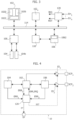
- FIG 2 shows a block diagram of an exemplary digital processing system 10, such as a micro-controller, which may be used as any of the processing systems 10 of Figure 1 .
- the processing system 10 comprises a microprocessor 102, usually the Central Processing Unit (CPU), programmed via software instructions.
- the software executed by the microprocessor 102 is stored in a non-volatile program memory 104, such as a Flash memory or EEPROM.
- the memory 104 is configured to store the firmware of the processing unit 102, wherein the firmware includes the software instructions to be executed by the microprocessor 102.
- the non-volatile memory 104 may also be used to store other data, such as configuration data, e.g., calibration data.
- the microprocessor 102 usually has associated also a volatile memory 104b, such as a Random-Access-Memory (RAM).
- a volatile memory 104b such as a Random-Access-Memory (RAM).
- RAM Random-Access-Memory
- the memory 104b may be used to store temporary data.
- the communication with the memories 104 and/or 104b is performed via one or more memory controllers 100.
- the memory controller(s) 100 may be integrated in the microprocessor 102 or connected to the microprocessor 102 via a communication channel, such as a system bus of the processing system 10.
- the memories 104 and/or 104b may be integrated with the microprocessor 102 in a single integrated circuit, or the memories 104 and/or 104b may be in the form of a separate integrated circuit and connected to the microprocessor 102, e.g., via the traces of a printed circuit board.
- the microprocessor 102 may have associated one or more (hardware) resources/peripherals 106 selected from the group of:
- a dedicated digital components DC may also correspond to a FPGA integrated in the processing system 10.
- the memory 104 may also comprise the program data for such a FPGA.
- the digital processing system 10 may support different functionalities.
- the behavior of the microprocessor 102 is determined by the firmware stored in the memory 104, e.g., the software instructions to be executed by a microprocessor 102 of a micro-controller 10.
- the firmware stored in the memory 104
- processing systems 10 e.g., micro-controllers adapted to be used in automotive applications
- micro-controllers are expected to exhibit an increase in complexity, mainly due to the increasing number of requested functionalities (new protocols, new features, etc.) and to the tight constraints of execution conditions (e.g., lower power consumption, increased calculation power and speed, etc.).
- the various error signals ERR 1 , ..., ERR m are provided to the fault collection and error management circuit 120.
- the fault collection and error management circuit 120 may execute various operations.
- the fault collection and error management circuit 120 may be configured to generate at least one of:
- the circuits of the processing system 10 may not operate correctly, possibly generating incorrect signals at the pins/pads of the processing system 10.
- Some of the pins/pads of the processing system 10a may thus be safety-critical pins/pad, i.e., pins/pads which may generate critical situations when driven incorrectly.
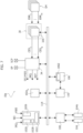
- Figure 4 is shown schematically a first safety-critical pin SCP 1 , which is driven by a processing core 102, and a second safety-critical pin SCP 2 , which is driven by a resource/peripheral 106, such as a communication interface or a PWM half-bridge driver.
- each input/output pin/pad of the processing system 10 has usually associated a respective driver circuit IO, which is configured to drive the respective pin/pad as a function of the signal received from the respective block, e.g., the processing system 102 and the hardware resources 106.
- a dedicated logic such as one or more multiplexers, permitting a configuration of the pin-mapping.
- the driver circuit IO of a safety-critical pins/pads SCP may be configured to set the output level of the respective pin to a given safety state in response to a signal SET.
- the output level such as a high-impedance state or a given logic level (high or low), may depend on the specific application needs.
- a "safety state" is compliant to the ISO2626 specification.
- Figure 5 shows a possible implementation of the fault collection and error management circuit 120.
- the fault collection and error management circuit 120 comprises a register 1200.
- the register 1200 comprises one or more error bits EB for storing the value of the error signals ERR.
- the register 1200 may comprise a corresponding number of error bits EB.
- the fault collection and error management circuit 120 comprises an internal reaction circuit 1202.
- the internal reaction circuit 1202 may be configured to generate the interrupt signal IRQ and/or the reset request signal RST as a function of the content of the error bits EB of the register 1200.
- the error bits EB are purely optional and the external reaction circuit 1202 may generate the interrupt signal IRQ and/or the reset request signal RST also directly as a function of the error signal(s) ERR.
- the fault collection and error management circuit 120 comprises an external reaction circuit 1204.
- the external reaction circuit 1204 may be configured to generate the error trigger signal ET and/or the signal SET as a function of the content of the error bits EB of the register 1200.
- the error bits EB are purely optional and the external reaction circuit 1204 may generate the signal ET and/or the signal SET also directly as a function of the error signal(s) ERR.
- the fault collection and error management circuit 120 may receive a significant number or error signals ERR from different circuits of the processing system. For example, this applies in particular to complex multi-core processing systems 10. For example, in the context of automotive applications, multiple functionalities, such as braking, airbag control, powertrain, etc., may be integrated on the same processing system. However, in this context, also the safety requirements prescribed by the ISO26262 specification have to be satisfied.
- the hardware error signals ERR are generated by dedicated safety monitor circuits SM.
- safety monitor circuits may comprise combinational and/or sequential logic circuits, which monitor the operation of a given circuit.
- safety monitor circuits SM may also comprise analog components, e.g., in order to detect an out-of-range condition for an analog signal, such as an internal supply voltage or a signal indicative of the operating temperature of the processing system or a specific circuit of the processing system.
- Figure 6 shows a safety monitor circuit SM 104 configured to monitor one or more signals of the memory 104, a safety monitor circuit SM 102 configured to monitor one or more signals of a processing core 102 and a safety monitor circuit SM 106 configured to monitor one or more signals of a resource/peripheral 106.
- the safety monitor circuit may also be integrated in the respective circuit.
- each safety monitor circuit SM monitors one or more signals generated by and/or provided to the associated circuit, and determines whether the behavior of the signal(s) is normal or indicates an error.
- the operations performed by a given safety monitor circuit SM depend on the associated circuit and may include, e.g .:
- the safety monitor circuit SM 104 may correspond to an error detection circuit of the memory 104, which calculates (via combinational and optionally sequential logic operations) an error correction code for the data read from the memory and compares (via combinational logic operations) the calculated error correction code with an error correction code read from the memory.
- the safety monitor circuit SM 102 may comprise a watch-dog timer configured to generate an error signal when the associated processing core does not reset the watch-dog timer in a given period of time.
- the safety monitor circuit SM may assert a respective error signal ERR, which signals the error to the fault collection system 120.
- document US 2016/210069 A1 discloses a host system for accessing guest memory in a hardware virtualisation environment having a hardware processor configured to determine, according to the contents of the override field, when permission override is enabled in response to memory access.
- the processing system 10a such as an integrated circuit, comprises:
- error signals ERR may have to be managed within the processing system 10a.
- error signals ERR are generated by safety monitoring circuits SM, which analyses the behavior of an associated circuit, such as a processing core 102, a memory controller 100 or a resource/peripheral 106.
- safety monitoring circuits SM may be associated with the same circuit and monitor different potential errors, such as one or more safety monitoring circuits monitoring different memory ranges of a memory 104 or 104b.
- safety monitoring circuits SM are positioned near or are even integrated in the associated circuit.
- each error signal ERR has to be provided via a respective trace to a respective input of the fault collection and error management circuit 120, which may thus involve a complex wiring within the processing system.
- each error combination circuits 320 such as error combination circuits 320 1 , ..., 320 p , wherein each error combination circuits 320 is configured to generate a combined error signal CES by combining a plurality of error signals ERR via a combinational logic operation, e.g ., via a logic OR operation.
- each combined error signal CES such as combined error signals CES 1 , ..., CES p
- the error combination circuits 320 may be positioned near the respective safety monitoring circuits SM.
- the combined error signal CES generated by an error combination circuits 320 may be stuck to a given logic level when one (or more) of the received error signals ERR itself are stuck to a given logic level, e.g ., set to high in case of a logic OR operation.
- a given error signal ERR may be asserted, either because the respective safety monitor circuit SM has detected an error or due to a malfunction of the safety monitor circuit SM itself.
- the error management circuit 34 is not anymore able to distinguish the error signals ERR having been combined into the respective combined error signal CES. Accordingly, in order to distinguish the errors again, either the safety monitor circuits SM and/or the fault collection sub-circuit 32 have to comprise a register used to store the error state, wherein the register is readable, e.g ., via software instructions executed on a processing core 102.
- each processing core 102a (or even each microprocessor 1020 in case the processing core 102a comprises plural microprocessors) comprises or has associated a hardware address protection circuit 1028 (see also Figure 7 ), such as a Memory Management Unit (MMU) or Memory Protection Unit (MPU), which manages the forwarding of the read or write requests generated by the processing core 102 to the communication system 114, e.g ., the forwarding of a read or write requests generated by a respective microprocessor 1020 to the communication interface 1022.
- MMU Memory Management Unit
- MPU Memory Protection Unit
- a Memory Management Unit which is used in a Virtual Memory System Architecture (VMSA), such as an ARM AArch64 architecture, permits to configure (e.g ., via the operating system OS) one or more translation tables (TTB).
- VMSA Virtual Memory System Architecture
- TTB translation tables
- a translation table permits to map a given virtual address to a respective physical address or a further virtual address.
- VA virtual addresses
- PA physical addresses
- the MMU may be configured to:
- a Memory Protection Unit which is used in a Protected Memory System Architecture (PMSA), such as an ARM AArch32 architecture with PMSA, does not perform an address translation.
- PMSA Protected Memory System Architecture
- the MPU instead of defining the mapping of virtual addresses to physical addresses, the MPU permits to specify, e.g ., via one or more access-right tables, directly the physical addresses/address ranges a software task executed by a microprocessor 1020 may access, e.g ., the MPU may be configured to:
- FIG. 9 shows moreover that recently it has been proposed to perform a virtualization, wherein a hypervisor HYP is executed by the processing system 10a.
- the hypervisor HYP essentially corresponds to a particular software layer, which permits the configuration of a plurality of k virtual machines VM 1 , ..., VM k , wherein each virtual machine VM may execute respective software tasks, such as a respective operating system OS and one or more respective applications APP.
- the value VMID is usually required, because a given microprocessor 1020 is not necessarily associated univocally to given respective virtual machine.
- a plurality of virtual machines may be executed (via a time scheduling scheme) on the same processing core 102a or a given virtual machine may be executed (in parallel or sequentially) by a plurality of microprocessor 1020.
- the hypervisor HYP may set the respective VMID of a given microprocessor 1020 when switching from one virtual machine to another.
- given resources 106 and/or given address ranges managed by a memory controller 100 may be assigned univocally to a given virtual machine VM or the hypervisor HYP.
- the hypervisor HYP may configure the processing system 10a such that a given resource 106, e.g ., a communication interface, is only accessible by a first virtual machine, but not by a second virtual machine.
- the protection circuit 1028 usually it is impossible to block via the protection circuit 1028 access to single bits of a register associated with a given physical address. Accordingly, the only way to limit the access of a given virtual machine to these error bits, and thus the respective register bits, resides in blocking the access for all virtual machines and permitting the access only for the hypervisor HYP, which thus may provide the respective error information to the virtual machine VM associated with the circuit having generated the error signal.
- the fault collection circuit 30 and the fault management circuit 34 are configured in a specific manner, which simplifies the management of the error signals ERR, in particular in the context of a multi-core processing system 10a, e.g., used to execute a plurality of k virtual machines VM.
- the fault collection circuit 30 comprising a plurality of fault collection sub-circuit 32, also identified as Combined Error Manager (CEM) circuit in the following.
- the fault collection circuit 30 comprises a number p of fault collection sub-circuit 32 1 , ..., 32 p .
- the number p of fault collection sub-circuit 32 corresponds to or is greater than:
- each virtual machine VM or each microprocessor 1020 is associated a respective fault collection sub-circuit 32.
- the processing system 10a may comprise a further fault collection sub-circuit 32 associated with the hypervisor HYP.
- the processing system 10a may comprise also a further fault collection sub-circuit 32, which may manage system errors not being specifically associated with a specific virtual machine VM or processing core 102a, such as errors being associated with monitored clock signals, supply voltages, temperature, etc.
- each fault collection sub-circuit/CEM circuit 32 comprises one or more programmable error combination circuits 320, e.g ., a number q of error combination circuits 320 1 , 1 , ..., 320 1 , q for the fault collection sub-circuit 32 1 .
- each error combination circuits 320 is configured to generate a respective combined error signal CES, e.g ., a combined error signals CES 1 , 1 , ..., CES 1 , q for the error combination circuits 320 1 , 1 , ..., 320 1 , q .
- each error combination circuits 320 receives a given number of s of error signals, e.g ., error signals ERR 1 , ..., ERR s .
- the number s of error signals ERR may be different for the error combination circuits 320 of a given fault collection sub-circuit 32 and/or may be different for the error combination circuits 320 of a different fault collection sub-circuit 32.
- a fault collection sub-circuit 32 may be associated univocally with each microprocessor 1020, wherein each sub-circuit 32 comprises one or more error combination circuits 320 configured to collect the errors associated with the respective microprocessor 102, such as errors generated by monitoring the respective microprocessor 1020 (see, e.g ., the safety monitoring circuit SM 102 in Figure 6 ), errors generated by monitoring predetermined memory ranges in the memory 104 and/or 104b assigned to the microprocessor 1020 (see, e. g. , the safety monitoring circuit SM 104 in Figure 6 ), and/or errors generated by monitoring respective components in the processing core 102a, such as the memory 1026, the protection unit 1028 and/or the interface 1022.
- error combination circuits 320 configured to collect the errors associated with the respective microprocessor 102, such as errors generated by monitoring the respective microprocessor 1020 (see, e.g ., the safety monitoring circuit SM 102 in Figure 6 ), errors generated by monitoring predetermined memory ranges in the memory
- each microprocessor 1020 executes, at a given instant, only a respective virtual machine VM, wherein also a plurality of micro-processors 1020 may be assigned to the same virtual machine, i.e ., each microprocessor 1020 is associated, at the given instant, univocally with a respective virtual machine.
- resources/peripherals 106 such resources may be assigned univocally to a given microprocessor 1020 or the assignment may be programmable, e.g ., by specifying the access rights as described with respect to the protection unit 1028.
- the error signals relating to resources 106 received by the various fault collection sub-circuit 32 may be different.
- the error signals generated for one or more resources 106 are managed by a fault collection sub-circuit 32 assigned to the hypervisor HYP, thereby performing a global management of the error signals relating to (shared) resources 106.
- each fault collection sub-circuit 32 associated with a microprocessor 1020 may receive the error signals ERR generated for a given resource 106, thereby permitting that each microprocessor 1020 may individually monitor the error signals of the given resource.
- low-speed communication interfaces e.g ., UART
- high-speed communication interfaces e.g. CAN or Ethernet
- error combination circuit 320 of an additional fault collection sub-circuit 32 may be assigned (via a suitable programming of the access rights) to a virtual machine VM or a microprocessor 1020.
- the number s of error signals of the error combination circuits 320 and the number q of error combination circuits 320 of a fault collection sub-circuit 32 are thus defined during the hardware design phase of the processing system 10a.
- each error combination circuits 320 receives a respective set of error signals ERR 1 , ..., ERR s , and generates a respective combined error signals CES.
- the combined error signals of the fault collection sub-circuit 32 are provided to the error management circuit 34.
- the error management circuit receives the combined error signals from the fault collection sub-circuit 32 1 (identified as CES 1,1 to CES 1,q ), the combined error signals from the fault collection sub-circuit 32 2 (identified simply as CES 2 ), etc.
- Figure 10 shows, at the example of the error combination circuits 320 1,1 , a possible embodiment of the error combination circuits 320.
- the error combination circuit 320 comprises:
- the register 3204 is connected (via a respective communication interface) to the communication system 114 and may thus be accessed via software instructions executed by a microprocessor 1020.
- Figure 11 shows a possible embodiment of a generic programmable error signal processing circuit 3200 i (which may be used for any of the circuits 3200) and the register 3204.
- the programmable error signal processing circuit 3200 i receives an error signal ERR i and provides a processed error signal ERR' i as a function of configuration data stored to the register 3204.
- the register 3204 comprises for each error signal processing circuit 3200 i two bits:
- the enable bits ENABLE in the register 3204 may be written by sending a request REQ via the communication system 114.
- the error status bit STATUS is asserted when the respective error signal ERR i is asserted and may be de-asserted by sending a request REQ via the communication system 114.
- the error status bit STATUS may be implemented with a set-reset flip-flop, wherein the error signal ERR i is connected to the set input and a respective bit of a request REQ received via the communication system 114 is connected to the reset input, i.e. , the bit STATUS may be implemented with a so-called write-1-clear register.
- the error status bit STATUS and the enable bit ENABLE are provided to a logic gate 3208, such as an AND gate, configured to assert the processed error signal ERR' i when both the error status bit STATUS and the enable bit ENABLE are asserted.
- a logic gate 3208 such as an AND gate
- the programmable error signal processing circuit 3200 i may also comprise a synchronization circuit 3206 arranged between the error signal ERR i and the input of the status bits STATUS.
- a synchronization circuit 3206 may be useful to normalize the characteristics of the input triggers connected to the error combination circuit 320.
- such a synchronization circuit 3206 may comprise a clock synchronization stage used to decouple the clock used by the respective safety monitor circuit SM from the clock used by the error combination circuit 320.
- such a clock synchronization stage may be implemented with a plurality of flip-flops connected in cascade, wherein these flip-flops use the clock signal of the error combination circuit 320, which preferably corresponds to the clock signal used by the error management circuit 34.
- the synchronization circuit 3206 may also perform other operations based on the properties of the received error signal ERR, e.g. , invert the logic level. Accordingly, by using the synchronization circuit 3206 and the status bit register STATUS, the characteristics of the combined error signals CES provided to the error management circuit 34 may be uniform.
- a microprocessor 1020 may specify which errors should be signaled via the respective combined error signal CES. For example, in various embodiments, the enabled bits ENABLE are by default asserted. Conversely, by reading the error status bit STATUS of the register 3204, a microprocessor 1020 may determine which error signals ERR triggered, which may thus be used to determine which error signal ERR was asserted and asserted the combined error signal CES.
- a processing core 102a may disable the error signals ERR of any safety monitoring circuit SM having a malfunction and having the error signal ERR always asserted.
- different clock monitor circuits SM may be inserted on various branches of the clock tree. The number of clock monitor circuits may be so high that it is convenient to combine the respective error signals ERR via one or more error combination circuit 320, thereby generating one or more combined error signals CES.
- clock-monitoring circuits associated specifically with a given microprocessor 1020 such as a PLL generating a clock signal, which is only provided to the respective microprocessor 1020, may be provided to the fault collection sub-circuit 32 associated with the respective microprocessor 1020.
- error signals generated by clock-monitoring circuits monitoring shared clock signals may be provided to one or more error combination circuit 320 of a dedicated fault collection sub-circuit 32, which, e.g ., may be managed by the hypervisor HYP.
Landscapes
- Engineering & Computer Science (AREA)
- Theoretical Computer Science (AREA)
- Physics & Mathematics (AREA)
- General Engineering & Computer Science (AREA)
- General Physics & Mathematics (AREA)
- Software Systems (AREA)
- Quality & Reliability (AREA)
- Mathematical Physics (AREA)
- Computer Vision & Pattern Recognition (AREA)
- Hardware Redundancy (AREA)
Claims (13)
- Verarbeitungssystem (10a), das so konfiguriert ist, dass es einen Hypervisor (HYP) und eine oder mehrere virtuelle Maschinen (VM) ausführt, wobei das Verarbeitungssystem (10a) Folgendes umfasst:- eine Vielzahl von Mikroprozessoren (1020), die über Softwareanweisungen programmierbar sind;- eine Speichersteuerung (100), die so konfiguriert ist, dass sie die Softwareanweisungen aus einem nichtflüchtigen Speicher (104) liest;- ein Peripheriegerät (106);- ein Kommunikationssystem (114), das die Mikroprozessoren (1020) mit der Speichersteuerung (100) und dem Peripheriegerät (106) verbindet;- eine Vielzahl von Sicherheitsüberwachungsschaltungen (SM), die so konfiguriert sind, dass sie eine Vielzahl von Fehlersignalen (ERR) erzeugen, indem sie den Betrieb der Mikroprozessoren (1020), der Speichersteuerung (100) und/oder des Peripheriegeräts (106) überwachen;- eine Fehlersammel- und Fehlermanagementschaltung (120), die für Folgendes konfiguriert ist:- Empfangen der Vielzahl von Fehlersignalen (ERR) von der Vielzahl von Sicherheitsüberwachungsschaltungen (SM), und- Erzeugen eines oder mehrerer Reaktionssignale (IRQ, IR2, ET, SET) als Funktion der Vielzahl von Fehlersignalen (ERR); wobei die Fehlersammel- und Fehlermanagementschaltung Folgendes umfasst:- eine Vielzahl von Fehlersammel-Unterschaltungen (32), wobei die Vielzahl von Fehlersammel-Unterschaltungen (32) für jeden Mikroprozessor (1020) oder jede virtuelle Maschine (VM) eine jeweilige Fehlersammel-Unterschaltung (32) umfasst, wobei jede Fehlersammel-Unterschaltung (32) eine oder mehrere Fehlerkombinationsschaltungen (320) umfasst, wobei jede Fehlerkombinationsschaltung (320) ein erstes Register (3204) umfasst, das über Softwareanweisungen, die von einem Mikroprozessor (1020) ausgeführt werden, programmierbar ist und für Folgendes konfiguriert ist:- Empfangen einer Teilmenge der Fehlersignale (ERR1, ..., ERRs),- Bestimmen, ob eines oder mehrere der empfangenen Fehlersignale (ERR1, ..., ERRs) aktiviert sind,- als Reaktion auf das Bestimmen, dass eines oder mehrere der empfangenen Fehlersignale (ERR1, ... , ERRs) aktiviert sind, Speichern von Fehlerstatusdaten (STATUS) in dem ersten Register (3204), wobei die Fehlerstatusdaten (STATUS) das eine oder die mehreren aktivierten Fehlersignale (ERR1, ... , ERRs) identifizieren,- Lesen von Freigabedaten (ENABLE) aus dem ersten Register (3204), wobei die Freigabedaten (ENABLE) für jedes Fehlersignal (ERR1, ..., ERRS) angeben, ob ein kombiniertes Fehlersignal (CES) aktiviert werden soll, wenn das jeweilige Fehlersignal (ERR1, ..., ERRs) aktiviert ist, und- Erzeugen (3208) des kombinierten Fehlersignals (CES) als Funktion der Fehlerstatusdaten (STATUS) und der Freigabedaten (ENABLE); und- eine Fehlermanagementschaltung (34), die ein zweites Register (340) umfasst, das über Softwareanweisungen, die von einem Mikroprozessor (1020) ausgeführt werden, programmierbar ist und für Folgendes konfiguriert ist:- Empfangen der kombinierten Fehlersignale (CES) von den Fehlerkombinationsschaltungen (320),- Lesen von Routingdaten (RD) aus dem zweiten Register (340), wobei die Routingdaten (RD) für jedes kombinierte Fehlersignal (CES) und für jeden Mikroprozessor (1020) angeben, ob ein Fehler (IRQ, SEI, VSEI) an den jeweiligen Mikroprozessor (1020) signalisiert werden soll, wenn das jeweilige kombinierte Fehlersignal (CES) aktiviert wird,- Bereitstellen eines jeweiligen Signals (IRQ, SEI, VSEI), das verwendet wird, um einen Fehler zu signalisieren, an jeden Mikroprozessor (1020), wobei die Signale (IRQ, SEI, VSEI) als Funktion der kombinierten Fehlersignale (CES) und der Routingdaten (RD) erzeugt werden;dadurch gekennzeichnet, dass das erste Register (3204) jeder Fehlerkombinationsschaltung (320) und das zweite Register (340) mit dem Kommunikationssystem (114) verbunden sind und eine oder mehrere jeweilige physikalische Adressen zugeordnet haben, und wobei das erste Register (3204) und das zweite Register (340) jeweils durch Senden einer Schreibanfrage (REQ), die die jeweilige physikalische Adresse umfasst, an das Kommunikationssystem (114) programmierbar sind, und wobei das Verarbeitungssystem (10a) eine oder mehrere Hardware-Adressschutzschaltungen (1028) umfasst, die so konfiguriert sind, dass sie die von den Mikroprozessoren (1020) erzeugte Schreibanforderung (REQ) selektiv an die ersten Register (3204) der Fehlerkombinationsschaltung (320) und das zweite Register (340) als Funktion von virtuellen Adressübersetzungsdaten und/oder Zugriffsrechtedaten weiterleiten, wobei der Hypervisor (HYP) so konfiguriert ist, dass er die virtuellen Adressübersetzungsdaten und/oder Zugriffsrechtedaten für jeden Mikroprozessor (1020) und/oder jede virtuelle Maschine (VM) programmiert, undwobei jedem Mikroprozessor (1020) ein Register zum Speichern einer virtuellen Maschinen-ID zugeordnet ist, wobei die Hardware-Adressschutzschaltung (1028) so konfiguriert ist, dass sie virtuelle Adressübersetzungsdaten und/oder Zugriffsrechtedaten als Funktion der virtuellen Maschinen-ID verwendet, die in dem dem Mikroprozessor (1020) zugeordneten Register gespeichert ist, und wobei der Hypervisor (HYP) für Folgendes konfiguriert ist:- Zuordnen einer jeweiligen virtuellen Maschinen-ID zu jeder virtuellen Maschine (VM),- Programmieren von jeweiligen virtuellen Adressübersetzungsdaten und/oder Zugriffsrechtedaten für jede virtuelle Maschinen-ID,- Bestimmen für jeden Mikroprozessor (1020), ob eine virtuelle Maschine (VM) ausgeführt werden soll, und- als Reaktion auf das Bestimmen, dass eine virtuelle Maschine (VM) auf einem Mikroprozessor (1020) ausgeführt werden soll, Programmieren der jeweiligen virtuellen Maschinen-ID in das dem Mikroprozessor (1020) zugeordnete Register und Starten der jeweiligen virtuellen Maschine (VM) auf dem Mikroprozessor (1020).
- Verarbeitungssystem (10a) nach Anspruch 1, wobei das Verarbeitungssystem (10a) so konfiguriert ist, dass es den Zugriff auf die in dem zweiten Register (340) gespeicherten Routingdaten (RD) nur über den Mikroprozessor (1020) ermöglicht, der den Hypervisor (HYP) ausführt.
- Verarbeitungssystem (10a) nach einem von Anspruch 1 oder Anspruch 2, wobei die Vielzahl von Fehlersammel-Unterschaltungen (32) eine dem Hypervisor (HYP) zugeordnete Fehlersammel-Unterschaltung (32) umfasst, wobei das Verarbeitungssystem (10a) so konfiguriert ist, dass es den Zugriff auf die ersten Register der einen oder der mehreren Fehlerkombinationsschaltungen (320) der dem Hypervisor (HYP) zugeordneten Fehlersammel-Unterschaltung (32) nur über den Mikroprozessor (1020) ermöglicht, der den Hypervisor (HYP) ausführt.
- Verarbeitungssystem (10a) nach Anspruch 3, wobei die dem Hypervisor (HYP) zugeordnete Fehlersammel-Unterschaltung (32) eine oder mehrere Fehlerkombinationsschaltungen (320) umfasst, die so konfiguriert sind, dass sie Systemfehlersignale und/oder Fehlersignale empfangen, die von einer oder mehreren Sicherheitsüberwachungsschaltungen (SM106) erzeugt werden, die so konfiguriert sind, dass sie den Betrieb eines oder mehrerer erster Peripheriegeräte (106) überwachen.
- Verarbeitungssystem (10a) nach einem der vorhergehenden Ansprüche, wobei der Hypervisor (HYP) so konfiguriert ist, dass er die virtuellen Adressübersetzungsdaten und/oder Zugriffsrechtedaten für jeden Mikroprozessor (1020) und/oder jede virtuelle Maschine (VM) programmiert, sodass:- jeder Mikroprozessor (1020) auf die ersten Register der einen oder der mehreren Fehlerkombinationsschaltungen (320) der dem Mikroprozessor (1020) zugeordneten Fehlersammel-Unterschaltung (32) zugreifen kann.
- Verarbeitungssystem (10a) nach Anspruch 5, wobei der Hypervisor (HYP) so konfiguriert ist, dass er die in dem zweiten Register (340) gespeicherten Routingdaten (RD) programmiert, um:- die von der einen oder den mehreren Fehlerkombinationsschaltungen (320) einer einem Mikroprozessor (1020) zugeordneten Fehlersammel-Unterschaltung (32) erzeugten kombinierten Fehlersignale (CES) an den jeweiligen Mikroprozessor (1020) weiterzuleiten.
- Verarbeitungssystem (10a) nach Anspruch 5 oder Anspruch 6, wobei die eine oder die mehreren der Fehlerkombinationsschaltungen (320) einer einem Mikroprozessor (1020) zugeordneten Fehlersammel-Unterschaltung (32) so konfiguriert sind, dass sie Fehlersignale (ERR) empfangen, die von einer oder mehreren Sicherheitsüberwachungsschaltungen (SM102) erzeugt werden, die so konfiguriert sind, dass sie den Betrieb des jeweiligen Mikroprozessors (1020) überwachen.
- Verarbeitungssystem (10a) nach Anspruch 7, wobei die eine oder die mehreren der Fehlerkombinationsschaltungen (320) einer einem Mikroprozessor (1020) zugeordneten Fehlersammel-Unterschaltung (32) so konfiguriert sind, dass sie Fehlersignale (ERR) empfangen, die von einer oder mehreren Sicherheitsüberwachungsschaltungen (SM106; SM104) erzeugt werden, die so konfiguriert sind, dass sie den Betrieb eines oder mehrerer sekundärer Peripheriegeräte (106) und/oder Speicherbereiche überwachen, die dem jeweiligen Mikroprozessor (1020) zugeordnet sind.
- Verarbeitungssystem (10a) nach einem der vorhergehenden Ansprüche 1 bis 4, wobei der Hypervisor (HYP) so konfiguriert ist, dass er die virtuellen Adressübersetzungsdaten und/oder Zugriffsrechtedaten für jeden Mikroprozessor (1020) und/oder jede virtuelle Maschine (VM) programmiert, sodass:- jede virtuelle Maschine (VM) auf die ersten Register der einen oder der mehreren Fehlerkombinationsschaltungen (320) der der virtuellen Maschine (VM) zugeordneten Fehlersammel-Unterschaltung (32) zugreifen kann.
- Verarbeitungssystem (10a) nach Anspruch 9, wobei der Hypervisor (HYP) so konfiguriert ist, dass er die in dem zweiten Register (340) gespeicherten Routingdaten (RD) programmiert, um:- die von der einen oder den mehreren Fehlerkombinationsschaltungen (320) einer einer virtuellen Maschine (VM) zugeordneten Fehlersammel-Unterschaltung (32) erzeugten kombinierten Fehlersignale (CES) an einen Mikroprozessor (1020) weiterzuleiten, der die jeweilige virtuelle Maschine (VM) ausführt.
- Integrierte Schaltung, die ein Verarbeitungssystem (10a) nach einem der vorstehenden Ansprüche umfasst.
- Vorrichtung, wie etwa ein Fahrzeug, die eine Vielzahl von Verarbeitungssystemen (10a) nach einem der vorstehenden Ansprüche 1 bis 10 umfasst, wobei die Verarbeitungssysteme (10a) über ein Kommunikationssystem (20) verbunden sind.
- Verfahren zum Betreiben eines Verarbeitungssystems (10a) nach einem der vorstehenden Ansprüche 1 bis 10, umfassend:- Programmieren der Freigabedaten (ENABLE) in ein oder mehrere der ersten Register (3204) der einen oder der mehreren Fehlerkombinationsschaltungen (320); und- Programmieren der Routingdaten (RD) in die zweiten Register (340) der Fehlermanagementschaltung (34).
Applications Claiming Priority (1)
| Application Number | Priority Date | Filing Date | Title |
|---|---|---|---|
| IT202100009683 | 2021-04-16 |
Publications (2)
| Publication Number | Publication Date |
|---|---|
| EP4075271A1 EP4075271A1 (de) | 2022-10-19 |
| EP4075271B1 true EP4075271B1 (de) | 2025-07-09 |
Family
ID=76808029
Family Applications (1)
| Application Number | Title | Priority Date | Filing Date |
|---|---|---|---|
| EP22167299.1A Active EP4075271B1 (de) | 2021-04-16 | 2022-04-08 | Verarbeitungssystem, zugehörige integrierte schaltung, vorrichtung und verfahren |
Country Status (3)
| Country | Link |
|---|---|
| US (1) | US12327129B2 (de) |
| EP (1) | EP4075271B1 (de) |
| CN (1) | CN115221084B (de) |
Families Citing this family (3)
| Publication number | Priority date | Publication date | Assignee | Title |
|---|---|---|---|---|
| JP2020517028A (ja) * | 2017-04-17 | 2020-06-11 | モービルアイ ヴィジョン テクノロジーズ リミテッド | 運転関連システムを含む安全なシステム |
| IT202200006455A1 (it) | 2022-04-01 | 2023-10-01 | Stmicroelectronics Application Gmbh | Sistema di elaborazione, relativo circuito integrato, dispositivo e procedimento |
| IT202400007039A1 (it) * | 2024-03-28 | 2025-09-28 | St Microelectronics Int Nv | Sistema di elaborazione, relativo circuito integrato, dispositivo e procedimento |
Family Cites Families (9)
| Publication number | Priority date | Publication date | Assignee | Title |
|---|---|---|---|---|
| US20070174679A1 (en) * | 2006-01-26 | 2007-07-26 | Ibm Corporation | Method and apparatus for processing error information and injecting errors in a processor system |
| US7653848B2 (en) * | 2006-07-14 | 2010-01-26 | International Business Machines Corporation | Selectively engaging optional data reduction mechanisms for capturing trace data |
| US9329919B2 (en) | 2008-07-16 | 2016-05-03 | Freescale Semiconductor, Inc. | Micro controller unit including an error indicator module |
| EP2609511B1 (de) * | 2010-08-26 | 2016-10-19 | Freescale Semiconductor, Inc. | Speicherverwaltungseinheit für ein mikroprozessorsystem, mikroprozessorsystem und verfahren zur speicherverwaltung |
| US20160210069A1 (en) | 2015-01-21 | 2016-07-21 | Bitdefender IPR Management Ltd. | Systems and Methods For Overriding Memory Access Permissions In A Virtual Machine |
| GB2563884B (en) | 2017-06-28 | 2020-01-08 | Advanced Risc Mach Ltd | Exception return instruction |
| JP6853162B2 (ja) * | 2017-11-20 | 2021-03-31 | ルネサスエレクトロニクス株式会社 | 半導体装置 |
| IT201800003234A1 (it) | 2018-03-02 | 2019-09-02 | Stmicroelectronics Application Gmbh | Sistema di elaborazione, relativo circuito integrato e procedimento |
| IT201800005506A1 (it) * | 2018-05-18 | 2019-11-18 | Sistema di elaborazione, relativo circuito integrato e procedimento |
-
2022
- 2022-04-04 US US17/657,856 patent/US12327129B2/en active Active
- 2022-04-08 EP EP22167299.1A patent/EP4075271B1/de active Active
- 2022-04-15 CN CN202210400090.8A patent/CN115221084B/zh active Active
Also Published As
| Publication number | Publication date |
|---|---|
| US12327129B2 (en) | 2025-06-10 |
| US20220334865A1 (en) | 2022-10-20 |
| CN115221084A (zh) | 2022-10-21 |
| CN115221084B (zh) | 2025-10-28 |
| EP4075271A1 (de) | 2022-10-19 |
Similar Documents
| Publication | Publication Date | Title |
|---|---|---|
| US12327129B2 (en) | Processing system, related integrated circuit, device and method | |
| JP5778283B2 (ja) | データ処理装置のデバッグ処理 | |
| US10002103B2 (en) | Low-pin microcontroller device with multiple independent microcontrollers | |
| EP3183657B1 (de) | Virtualisierung eines speichers für programmierbare logik | |
| US12061530B2 (en) | Processing system, related integrated circuit, device and method | |
| US12530215B2 (en) | Processing system, related integrated circuit, device and method for controlling communication over a communication system having a physical address range | |
| US10002102B2 (en) | Low-pin microcontroller device with multiple independent microcontrollers | |
| CN115309678B (zh) | 处理系统、相关集成电路、设备及方法 | |
| US20230314506A1 (en) | Processing system, related integrated circuit, device and method | |
| EP4254196B1 (de) | Verarbeitungssystem, zugehörige integrierte schaltung, vorrichtung und verfahren | |
| US12353880B2 (en) | One-time programmable (OTP) memory controller with a control circuit configured to assert a pre-load start signal and a pre-load end signal, related processing system, integrated circuit and method | |
| US9952913B2 (en) | Centralized peripheral access protection | |
| JP6679419B2 (ja) | メモリ保護ユニット、メモリ管理ユニット、及びマイクロコントローラ | |
| US12468638B2 (en) | Processing system, related integrated circuit, apparatus and method | |
| US12117942B2 (en) | Processing system, related integrated circuit, device and method | |
| EP4625174A1 (de) | Verarbeitungssystem, zugehörige integrierte schaltung, vorrichtung und verfahren | |
| Brewerton et al. | Hardware based paravirtualization: simplifying the co-hosting of legacy code for mixed criticality applications | |
| JPH09190401A (ja) | 周辺モジュールおよびマイクロプロセッサ・システム | |
| CN120724930A (zh) | 处理系统、相关集成电路、设备和方法 | |
| CN119046998A (zh) | 处理系统、相关的集成电路、装置以及方法 | |
| Bradley | Migrating from TMS320DM6446 to TMS320DM6437 |
Legal Events
| Date | Code | Title | Description |
|---|---|---|---|
| PUAI | Public reference made under article 153(3) epc to a published international application that has entered the european phase |
Free format text: ORIGINAL CODE: 0009012 |
|
| STAA | Information on the status of an ep patent application or granted ep patent |
Free format text: STATUS: THE APPLICATION HAS BEEN PUBLISHED |
|
| AK | Designated contracting states |
Kind code of ref document: A1 Designated state(s): AL AT BE BG CH CY CZ DE DK EE ES FI FR GB GR HR HU IE IS IT LI LT LU LV MC MK MT NL NO PL PT RO RS SE SI SK SM TR |
|
| STAA | Information on the status of an ep patent application or granted ep patent |
Free format text: STATUS: REQUEST FOR EXAMINATION WAS MADE |
|
| 17P | Request for examination filed |
Effective date: 20230223 |
|
| RBV | Designated contracting states (corrected) |
Designated state(s): AL AT BE BG CH CY CZ DE DK EE ES FI FR GB GR HR HU IE IS IT LI LT LU LV MC MK MT NL NO PL PT RO RS SE SI SK SM TR |
|
| STAA | Information on the status of an ep patent application or granted ep patent |
Free format text: STATUS: EXAMINATION IS IN PROGRESS |
|
| 17Q | First examination report despatched |
Effective date: 20240130 |
|
| GRAP | Despatch of communication of intention to grant a patent |
Free format text: ORIGINAL CODE: EPIDOSNIGR1 |
|
| STAA | Information on the status of an ep patent application or granted ep patent |
Free format text: STATUS: GRANT OF PATENT IS INTENDED |
|
| RIC1 | Information provided on ipc code assigned before grant |
Ipc: G06F 11/30 20060101ALI20250402BHEP Ipc: G06F 11/07 20060101ALI20250402BHEP Ipc: G06F 9/455 20180101AFI20250402BHEP |
|
| INTG | Intention to grant announced |
Effective date: 20250416 |
|
| GRAS | Grant fee paid |
Free format text: ORIGINAL CODE: EPIDOSNIGR3 |
|
| GRAA | (expected) grant |
Free format text: ORIGINAL CODE: 0009210 |
|
| STAA | Information on the status of an ep patent application or granted ep patent |
Free format text: STATUS: THE PATENT HAS BEEN GRANTED |
|
| AK | Designated contracting states |
Kind code of ref document: B1 Designated state(s): AL AT BE BG CH CY CZ DE DK EE ES FI FR GB GR HR HU IE IS IT LI LT LU LV MC MK MT NL NO PL PT RO RS SE SI SK SM TR |
|
| REG | Reference to a national code |
Ref country code: GB Ref legal event code: FG4D |
|
| REG | Reference to a national code |
Ref country code: CH Ref legal event code: EP |
|
| REG | Reference to a national code |
Ref country code: IE Ref legal event code: FG4D |
|
| REG | Reference to a national code |
Ref country code: DE Ref legal event code: R096 Ref document number: 602022017173 Country of ref document: DE |
|
| REG | Reference to a national code |
Ref country code: NL Ref legal event code: MP Effective date: 20250709 |
|
| PG25 | Lapsed in a contracting state [announced via postgrant information from national office to epo] |
Ref country code: PT Free format text: LAPSE BECAUSE OF FAILURE TO SUBMIT A TRANSLATION OF THE DESCRIPTION OR TO PAY THE FEE WITHIN THE PRESCRIBED TIME-LIMIT Effective date: 20251110 |
|
| PG25 | Lapsed in a contracting state [announced via postgrant information from national office to epo] |
Ref country code: NL Free format text: LAPSE BECAUSE OF FAILURE TO SUBMIT A TRANSLATION OF THE DESCRIPTION OR TO PAY THE FEE WITHIN THE PRESCRIBED TIME-LIMIT Effective date: 20250709 |
|
| REG | Reference to a national code |
Ref country code: AT Ref legal event code: MK05 Ref document number: 1812470 Country of ref document: AT Kind code of ref document: T Effective date: 20250709 |
|
| PG25 | Lapsed in a contracting state [announced via postgrant information from national office to epo] |
Ref country code: IS Free format text: LAPSE BECAUSE OF FAILURE TO SUBMIT A TRANSLATION OF THE DESCRIPTION OR TO PAY THE FEE WITHIN THE PRESCRIBED TIME-LIMIT Effective date: 20251109 |
|
| PG25 | Lapsed in a contracting state [announced via postgrant information from national office to epo] |
Ref country code: NO Free format text: LAPSE BECAUSE OF FAILURE TO SUBMIT A TRANSLATION OF THE DESCRIPTION OR TO PAY THE FEE WITHIN THE PRESCRIBED TIME-LIMIT Effective date: 20251009 |
|
| REG | Reference to a national code |
Ref country code: LT Ref legal event code: MG9D |
|
| PG25 | Lapsed in a contracting state [announced via postgrant information from national office to epo] |
Ref country code: AT Free format text: LAPSE BECAUSE OF FAILURE TO SUBMIT A TRANSLATION OF THE DESCRIPTION OR TO PAY THE FEE WITHIN THE PRESCRIBED TIME-LIMIT Effective date: 20250709 |
|
| PG25 | Lapsed in a contracting state [announced via postgrant information from national office to epo] |
Ref country code: FI Free format text: LAPSE BECAUSE OF FAILURE TO SUBMIT A TRANSLATION OF THE DESCRIPTION OR TO PAY THE FEE WITHIN THE PRESCRIBED TIME-LIMIT Effective date: 20250709 |
|
| PG25 | Lapsed in a contracting state [announced via postgrant information from national office to epo] |
Ref country code: HR Free format text: LAPSE BECAUSE OF FAILURE TO SUBMIT A TRANSLATION OF THE DESCRIPTION OR TO PAY THE FEE WITHIN THE PRESCRIBED TIME-LIMIT Effective date: 20250709 |
|
| PG25 | Lapsed in a contracting state [announced via postgrant information from national office to epo] |
Ref country code: GR Free format text: LAPSE BECAUSE OF FAILURE TO SUBMIT A TRANSLATION OF THE DESCRIPTION OR TO PAY THE FEE WITHIN THE PRESCRIBED TIME-LIMIT Effective date: 20251010 |
|
| PG25 | Lapsed in a contracting state [announced via postgrant information from national office to epo] |
Ref country code: SE Free format text: LAPSE BECAUSE OF FAILURE TO SUBMIT A TRANSLATION OF THE DESCRIPTION OR TO PAY THE FEE WITHIN THE PRESCRIBED TIME-LIMIT Effective date: 20250709 |
|
| PG25 | Lapsed in a contracting state [announced via postgrant information from national office to epo] |
Ref country code: LV Free format text: LAPSE BECAUSE OF FAILURE TO SUBMIT A TRANSLATION OF THE DESCRIPTION OR TO PAY THE FEE WITHIN THE PRESCRIBED TIME-LIMIT Effective date: 20250709 |
|
| PG25 | Lapsed in a contracting state [announced via postgrant information from national office to epo] |
Ref country code: PL Free format text: LAPSE BECAUSE OF FAILURE TO SUBMIT A TRANSLATION OF THE DESCRIPTION OR TO PAY THE FEE WITHIN THE PRESCRIBED TIME-LIMIT Effective date: 20250709 Ref country code: BG Free format text: LAPSE BECAUSE OF FAILURE TO SUBMIT A TRANSLATION OF THE DESCRIPTION OR TO PAY THE FEE WITHIN THE PRESCRIBED TIME-LIMIT Effective date: 20250709 |
|
| PG25 | Lapsed in a contracting state [announced via postgrant information from national office to epo] |
Ref country code: RS Free format text: LAPSE BECAUSE OF FAILURE TO SUBMIT A TRANSLATION OF THE DESCRIPTION OR TO PAY THE FEE WITHIN THE PRESCRIBED TIME-LIMIT Effective date: 20251009 |
|
| PG25 | Lapsed in a contracting state [announced via postgrant information from national office to epo] |
Ref country code: ES Free format text: LAPSE BECAUSE OF FAILURE TO SUBMIT A TRANSLATION OF THE DESCRIPTION OR TO PAY THE FEE WITHIN THE PRESCRIBED TIME-LIMIT Effective date: 20250709 |
|
| PG25 | Lapsed in a contracting state [announced via postgrant information from national office to epo] |
Ref country code: SM Free format text: LAPSE BECAUSE OF FAILURE TO SUBMIT A TRANSLATION OF THE DESCRIPTION OR TO PAY THE FEE WITHIN THE PRESCRIBED TIME-LIMIT Effective date: 20250709 |
|
| PG25 | Lapsed in a contracting state [announced via postgrant information from national office to epo] |
Ref country code: DK Free format text: LAPSE BECAUSE OF FAILURE TO SUBMIT A TRANSLATION OF THE DESCRIPTION OR TO PAY THE FEE WITHIN THE PRESCRIBED TIME-LIMIT Effective date: 20250709 |
|
| PG25 | Lapsed in a contracting state [announced via postgrant information from national office to epo] |
Ref country code: IT Free format text: LAPSE BECAUSE OF FAILURE TO SUBMIT A TRANSLATION OF THE DESCRIPTION OR TO PAY THE FEE WITHIN THE PRESCRIBED TIME-LIMIT Effective date: 20250709 |
|
| PG25 | Lapsed in a contracting state [announced via postgrant information from national office to epo] |
Ref country code: CZ Free format text: LAPSE BECAUSE OF FAILURE TO SUBMIT A TRANSLATION OF THE DESCRIPTION OR TO PAY THE FEE WITHIN THE PRESCRIBED TIME-LIMIT Effective date: 20250709 |
|
| PG25 | Lapsed in a contracting state [announced via postgrant information from national office to epo] |
Ref country code: SK Free format text: LAPSE BECAUSE OF FAILURE TO SUBMIT A TRANSLATION OF THE DESCRIPTION OR TO PAY THE FEE WITHIN THE PRESCRIBED TIME-LIMIT Effective date: 20250709 Ref country code: EE Free format text: LAPSE BECAUSE OF FAILURE TO SUBMIT A TRANSLATION OF THE DESCRIPTION OR TO PAY THE FEE WITHIN THE PRESCRIBED TIME-LIMIT Effective date: 20250709 |
|
| PLBE | No opposition filed within time limit |
Free format text: ORIGINAL CODE: 0009261 |
|
| STAA | Information on the status of an ep patent application or granted ep patent |
Free format text: STATUS: NO OPPOSITION FILED WITHIN TIME LIMIT |