EP4072028B1 - Mikroenergiegewinnungsvorrichtung und verfahren - Google Patents
Mikroenergiegewinnungsvorrichtung und verfahren Download PDFInfo
- Publication number
- EP4072028B1 EP4072028B1 EP19955011.2A EP19955011A EP4072028B1 EP 4072028 B1 EP4072028 B1 EP 4072028B1 EP 19955011 A EP19955011 A EP 19955011A EP 4072028 B1 EP4072028 B1 EP 4072028B1
- Authority
- EP
- European Patent Office
- Prior art keywords
- micro
- voltage
- radio frequency
- microprocessor
- energy
- Prior art date
- Legal status (The legal status is an assumption and is not a legal conclusion. Google has not performed a legal analysis and makes no representation as to the accuracy of the status listed.)
- Active
Links
Images


Classifications
-
- H—ELECTRICITY
- H02—GENERATION; CONVERSION OR DISTRIBUTION OF ELECTRIC POWER
- H02J—CIRCUIT ARRANGEMENTS OR SYSTEMS FOR SUPPLYING OR DISTRIBUTING ELECTRIC POWER; SYSTEMS FOR STORING ELECTRIC ENERGY
- H02J50/00—Circuit arrangements or systems for wireless supply or distribution of electric power
- H02J50/001—Energy harvesting or scavenging
-
- H—ELECTRICITY
- H02—GENERATION; CONVERSION OR DISTRIBUTION OF ELECTRIC POWER
- H02J—CIRCUIT ARRANGEMENTS OR SYSTEMS FOR SUPPLYING OR DISTRIBUTING ELECTRIC POWER; SYSTEMS FOR STORING ELECTRIC ENERGY
- H02J50/00—Circuit arrangements or systems for wireless supply or distribution of electric power
- H02J50/20—Circuit arrangements or systems for wireless supply or distribution of electric power using microwaves or radio frequency waves
-
- H—ELECTRICITY
- H04—ELECTRIC COMMUNICATION TECHNIQUE
- H04B—TRANSMISSION
- H04B1/00—Details of transmission systems, not covered by a single one of groups H04B3/00 - H04B13/00; Details of transmission systems not characterised by the medium used for transmission
- H04B1/38—Transceivers, i.e. devices in which transmitter and receiver form a structural unit and in which at least one part is used for functions of transmitting and receiving
- H04B1/40—Circuits
-
- Y—GENERAL TAGGING OF NEW TECHNOLOGICAL DEVELOPMENTS; GENERAL TAGGING OF CROSS-SECTIONAL TECHNOLOGIES SPANNING OVER SEVERAL SECTIONS OF THE IPC; TECHNICAL SUBJECTS COVERED BY FORMER USPC CROSS-REFERENCE ART COLLECTIONS [XRACs] AND DIGESTS
- Y02—TECHNOLOGIES OR APPLICATIONS FOR MITIGATION OR ADAPTATION AGAINST CLIMATE CHANGE
- Y02D—CLIMATE CHANGE MITIGATION TECHNOLOGIES IN INFORMATION AND COMMUNICATION TECHNOLOGIES [ICT], I.E. INFORMATION AND COMMUNICATION TECHNOLOGIES AIMING AT THE REDUCTION OF THEIR OWN ENERGY USE
- Y02D30/00—Reducing energy consumption in communication networks
- Y02D30/70—Reducing energy consumption in communication networks in wireless communication networks
Definitions
- the present application relates to the field of energy acquisition and conversion, and particularly relates to a micro-energy acquisition device and a micro-energy acquisition method.
- Micro-energy voltage of a conventional micro-energy acquisition device is input into a power terminal of a microprocessor and a power terminal of a radio frequency circuit respectively, the microprocessor generates a data signal according to the micro-energy voltage and outputs the data signal through a second input/output port; the radio frequency circuit generates a wireless communication signal according to the micro-energy voltage and the data signal, and transmits the wireless communication signal over a wireless link. Due to the fact that signal conversion and transmission of wireless communication signal can only be performed after crystal oscillator is powered up, parameters are configured, a phase-locked loop and a power amplifier are powered up.
- a prior art document D1 ( CN106611924A ) provides a communication device, a switching device and a communication system.
- the communication system includes a master communication device and a death communication device.
- the master communication device includes a first external interface constituted of a first pin and a second pin and a signal generating module electrically connected with the first pin.
- the signal generating module is used for generating X signals according to a time interval corresponding to bit string to be transmitted and having a length N.
- the time interval between a start time of each signal and a start time of an adjacent previous signal is the time interval corresponding to the bit string to be transmitted and having the length N. Time intervals corresponding to different bit strings are different.
- N is greater than or equal to 1.
- X is greater than or equal to 1, and X is a natural number.
- the first external interface is used for transmitting the X signals through the first pin.
- a prior document D2 ( US2015131771 ) provides a shift register unit and driving method thereof, a gate driving circuit and display device.
- the shift register unit utilizes the voltage stabilizing capacitor (C2) to stabilize the potential at the pull-up node (P), so as to make the signal output from the shift register unit more stable; and at the same time, uses a very small quantity of transistors and capacitors to compose the shift register unit, so that the wiring area of the gate driving circuit is greatly reduced to provide a technical support for the design of a liquid crystal display device with a narrower frame.
- the shift register unit quickly and effectively pulls down the output signal to the low potential through two pull-down processes, thereby enhancing the pull-down capability of the gate driving circuit.
- the present application provides a micro-energy acquisition device and a micro-energy acquisition method, which aims to solve a problem in the conventional micro-energy acquisition device that a power consumption speed of electric energy is fast since the microprocessor and the radio frequency circuit are connected in parallel, the micro-energy voltage cannot provide the radio frequency circuit with enough energy for transmitting complete data packet in the manner of wireless communication signal, thus, the deficiencies of weak capability of data transmission and high error rate of data transmission are caused.
- micro-energy acquisition device including:
- the microprocessor further includes a second input/output port connected with the radio frequency circuit;
- the switch circuit includes a first triode and a first resistance; where a base electrode of the first triode is connected with a first end of the first resistance, a second end of the first resistance is a control signal input of the switch circuit, a collector electrode of the first triode is a first voltage input of the switch circuit, and an emitting electrode of the first triode is connected with the power ground.
- the micro-energy acquisition device further includes:
- the third input/output port of the microprocessor is connected with the radio frequency circuit and the first unidirectional conduction component; the third input/output port of the microprocessor is a pull-down port with a low internal resistance;
- the first unidirectional conduction component includes a first diode.
- the micro-energy acquisition device further includes:
- the micro-energy acquisition device further includes:
- the rectifier circuit includes a second diode, a third diode, a fourth diode, and a fifth diode; where a positive electrode of the third diode and a negative electrode of the second diode are served as a first original micro-energy alternating current input of the rectifier circuit, a positive electrode of the fifth diode and a negative electrode of the fourth diode are served as a second original micro-energy alternating current input of the rectifier circuit, a negative electrode of the third diode and a negative electrode of the fifth diode constitute an original micro-energy voltage output of the rectifier circuit, and a positive electrode of the second diode and a positive electrode of the fourth diode are commonly connected with the power ground.
- the radio frequency circuit includes a radio frequency circuit chip, a crystal oscillator, an antenna, a first inductance, a second inductance, a third inductance, a fourth inductance, a second capacitance, a third capacitance, a fourth capacitance, a fifth capacitance and a sixth capacitance; a crystal oscillator terminal of the radio frequency circuit chip is connected with a first end of the crystal oscillator; a ground terminal of the radio frequency circuit chip is a ground terminal voltage output of the radio frequency circuit; a data terminal of the radio frequency circuit chip is a data signal input of the radio frequency circuit; a power terminal of the radio frequency circuit chip, a first end of the third capacitance, a first end of the sixth capacitance, and a first end of the first inductance constitute a micro-energy voltage input of the radio frequency circuit; a radio frequency terminal of the radio frequency circuit chip is connected with a second end of the first inductance and a first end of the second capacitance,
- a micro-energy acquisition method is further provided in one embodiment of the present application, the micro-energy acquisition method is based on the aforesaid micro-energy acquisition device, and includes:
- the micro-energy acquisition device in the embodiments of the present application includes the radio frequency circuit, the first unidirectional conduction component, and the microprocessor; the radio frequency circuit generates the ground voltage according to the micro-energy voltage and output the ground voltage through the ground terminal; the first unidirectional conduction component makes the ground voltage to flow unidirectionally so as to generate the first voltage; the microprocessor generates the supply voltage according to the first voltage and is operated according to the supply voltage; where the microprocessor includes the first input/output port which is provided with the pull-up switch transistor, the capacitance between the gate electrode and the source electrode of the pull-up switch transistor is charged according to the first voltage, and the charging voltage is generated, the pull-up switch transistor is turned on according to the charging voltage, so that the drain electrode of the pull-up switch transistor is powered up and the supply voltage is generated, and the microprocessor is operated according to the supply voltage; the first input/output port of the microprocessor is connected with the first unidirectional conduction component; since the microprocessor and the radio frequency circuit are connected
- FIG. 1 illustrates a modular structure of a micro-energy acquisition device according to one embodiment of the present application, for the convenience of description, the part related to the embodiments of the present application is merely illustrated, and this part is described in detail below:
- the micro-energy acquisition device includes a radio frequency circuit 01, a first unidirectional conduction component 02, and a microprocessor U10.
- the radio frequency circuit 01 is configured to generate a ground voltage according to the micro-energy voltage VCC and output a ground voltage through the ground terminal;
- the first unidirectional conduction component 02 is connected with the radio frequency circuit 01 and is configured to enable an unidirectional conduction ground voltage to generate a first voltage;
- the microprocessor U10 is connected with the first unidirectional conduction component 02 and is configured to generate a supply voltage according to the first voltage and is operated according to the supply voltage.
- the microprocessor U10 includes a first input/output port PC0, and a pull-up switch transistor M1 is provided in the first input/output port PC0, a capacitance CGS between a gate electrode and a source electrode of the pull-up switch transistor M1 is charged according to the first voltage to generate a charging voltage, and the pull-up switch transistor M1 is turned on according to the charging voltage to enable a drain electrode of the pull-up switch transistor M1 to be powered up to generate the supply voltage, and the microprocessor U10 is operated according to the supply voltage; the first input/output port PC0 of the microprocessor U10 is connected with the first unidirectional conduction component.
- the pull-up switch transistor M1 is turned on according to the charging voltage, so that the drain electrode of the pull-up switch transistor M1 is powered up and generates the supply voltage.
- the microprocessor U10 is operated according to the supply voltage, which specifically includes: the pull-up switch transistor M1 is turned on according to the charging voltage, the first voltage flows into the drain electrode of the pull-up switch transistor M1 through the source electrode and the gate electrode of the pull-up switch transistor M1 and generates the supply voltage, and the microprocessor U10 provides power supply for the various input/output ports thereof according to the supply voltage.
- the radio frequency circuit 01 After the radio frequency circuit 01 is powered up, powering on of a crystal oscillator, parameter configuration, powering on of a phase-locked loop and powering on of a power amplifier are firstly performed, then, signal conversion and transmission of wireless communication signal are performed; as for the micro-energy voltage VCC, since the microprocessor U10 and the radio frequency circuit 01 are connected in series, electric energy consumption of the micro-energy voltage VCC is slower, time spent on signal conversion and transmission of wireless communication signal are greatly prolonged, so that a capability of data transmission is improved, and an error rate of data transmission is reduced. In actual operation, a maintenance time of electric quantity of the micro-energy voltage VCC and code-transmitting time can reach more than 728 ⁇ s, which is equivalent to transmission of four data packets.
- a certain voltage drop is generated between the ground voltage and the first voltage through the first unidirectional conduction component 02, so that a service time of the micro-energy voltage VCC is further prolonged, the capability of data transmission is improved, and the error rate of data transmission is reduced.
- the second input/output port of the microprocessor U10 is connected with the radio frequency circuit 01; the microprocessor U10 is further configured to generate a data signal according to the supply voltage and output the data signal through the second input/output port; the radio frequency circuit 01 is further configured to generate a wireless communication signal according to the data signal and send the wireless communication signal through a wireless link.
- the micro-energy acquisition device further includes a switch circuit 03.
- the switch circuit 03 is connected with the radio frequency circuit 01 and the first unidirectional conduction component 02, and is configured to make the first voltage to be conductive with the power ground according to the control signal; the microprocessor U10 is further configured to generate the control signal according to the supply voltage; and the control signal is output through a third input/output port of the microprocessor U10.
- the first voltage is conductive with the power ground through the switch circuit 03, so that the ground terminal of the radio frequency circuit 01 is stabilized at a stable low level, and the stability and the reliability of operation of the radio frequency circuit 01 are improved.
- the micro-energy acquisition device further includes a second unidirectional conduction component 04.
- the second unidirectional conduction component 04 is connected with the radio frequency circuit 01 and the first unidirectional conduction component 02, and is configured to make the first voltage to flow unidirectionally; and the switch circuit 03 is specifically configured to make the first voltage that flows unidirectionally to be conductive with the power ground according to the control signal.
- the third input/output port of the microprocessor U10 is connected with the radio frequency circuit 01 and the first unidirectional conduction component 02; where the third input/output port of the microprocessor U10 is a pull-down port with large current and low internal resistance.
- the microprocessor U10 is further configured to generate the control signal according to the supply voltage.
- the control signal is output through the third input/output port of the microprocessor U10.
- the microprocessor U10 By connecting the third input/output port (i.e., the pull-down port with large current and low internal resistance) of the microprocessor U10 with the radio frequency circuit 01 and the first unidirectional conduction component 02, so that the microprocessor U10 generates the control signal according to the supply voltage, and the first voltage is conductive with the power ground, so that the ground terminal of the radio frequency circuit 01 is stabilized at the stable low level, the stability and the reliability of operation of the radio frequency circuit 01 are improved.
- the third input/output port i.e., the pull-down port with large current and low internal resistance
- the micro-energy acquisition device further includes a first energy storage element 05.
- first energy storage element 05 is connected with a power terminal of the microprocessor U10, and is configured to store electric energy according to the supply voltage and provide a second voltage; and the microprocessor U10 is further configured to be operated according to the second voltage.
- the micro-energy voltage VCC appears as an irregular steamed bun waveform
- the first energy storage element 05 stores the electric energy according to the supply voltage and provides the second voltage
- powering-on and working time of the microprocessor U10 are improved, the capability of data transmission is improved and the error rate of data transmission is reduced accordingly.
- the micro-energy acquisition device further includes a rectifier circuit 06 and a second energy storage element 08.
- the rectifier circuit 06 is connected with the radio frequency circuit 01, and is configured to generate an original micro-energy voltage VBB according to the original micro-energy alternating current VAA.
- the second energy storage element 08 is connected with the radio frequency circuit 01 and the rectifier circuit 06, and is configured to store electric energy according to the original micro-energy voltage VBB and output the micro-energy voltage VCC.
- micro-energy voltage VCC is generated by the rectifier circuit 06 and the second energy storage element 08 according to the original micro-energy alternating current VAA, so that the stability of the micro-energy voltage VCC is improved, and the stability and the reliability of the micro-energy acquisition device are improved.
- the micro-energy acquisition device further includes an indication component 07.
- the indication component 07 is connected with the microprocessor U10, and is configured to perform indication according to the micro-energy voltage and an indication signal.
- the microprocessor U10 is further configured to output the indication signal through a fourth input/output port thereof after outputting the data signal through the second input/output port.
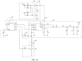
- FIG. 9 illustrates an exemplary circuit configuration of the micro-energy acquisition device according to one embodiment of the present application, for the convenience of description, a part related to the embodiments of the present application is only shown, the part related to the embodiments of the present application is described in detail below:
- the first unidirectional conduction component 02 includes a first diode D1.
- the rectifier circuit 06 includes a second diode D2, a third diode D3, a fourth diode D4, a fifth diode D5, and a first capacitance C1.
- a positive electrode of the third diode D3 and a negative electrode of the second diode D2 are served as a first original micro-energy alternating current VAA input of the rectifier circuit 06
- a negative electrode of the fifth diode D5 and a negative electrode of the fourth diode D4 are served as a second original micro-energy alternating current VAA input of the rectifier circuit 06
- a negative electrode of the third diode D3 and a negative electrode of the fifth diode D5 constitute a micro-energy voltage VCC output of the rectifier circuit 06
- a positive electrode of the second diode D2 and a positive electrode of the fourth diode D4 are commonly connected with the power ground.
- the second energy storage element 08 includes the first capacitance C1.
- the radio frequency circuit 01 includes a radio frequency circuit chip U1, a crystal oscillator Y1, an antenna ANT, a first inductance L1, a second inductance L2, a third inductance L3, a fourth inductance L4, a second capacitance C2, a third capacitance C3, a fourth capacitance C4, a fifth capacitance C5, and a sixth capacitance C6.
- a crystal oscillator terminal XTAL of the radio frequency circuit chip U1 is connected with a first end of the crystal oscillator Y1; a ground terminal GND of the radio frequency circuit chip U1 is a ground terminal voltage output of the radio frequency circuit 01; a data terminal DATA of the radio frequency circuit chip U1 is a data signal input of the radio frequency circuit 01; a power terminal VDD of the radio frequency circuit chip 01, a first end of the third capacitance C3, a first end of the sixth capacitance C6, and a first end of the first inductance L1 constitute a micro-energy voltage VCC input of the radio frequency circuit 01; a radio frequency terminal RFO of the radio frequency circuit chip is connected with a second end of the first inductance L1 and a first end of the second capacitance C2; a second end of the second capacitance C2 is connected with a first end of the second inductance L2, a second end of the second inductance L2 is connected with a first end of the fourth capacitance C4
- the first input/output port PC0 of the microprocessor U 10 is a first voltage input of the microprocessor U 10; the second input/output port PC1 of the microprocessor U10 is a data signal output of the microprocessor U 10, and the third input/output port PC2 of the microprocessor U10 is a control signal output of the microprocessor U10.
- the second unidirectional conduction component 04 includes a sixth diode D6.
- the first energy storage element 05 includes a seventh capacitance C7.
- the circuit configuration shown in FIG. 9 and FIG. 2 is further described below with reference to the working principle of the micro-energy acquisition device:
- the original micro-energy alternating current VAA is rectified to generate the original micro-energy voltage through the second diode D2, the third diode D3, the fourth diode D4 and the fifth diode D5, and the first capacitance C1 stores the electric energy according to the original micro-energy voltage and outputs the micro-energy voltage VCC;
- the micro-energy voltage VCC is input into the power terminal VDD of the radio frequency circuit chip U1, the radio frequency circuit chip U1 generates the ground voltage according to the micro-energy voltage VCC and outputs the ground voltage through the ground terminal GND of the radio frequency circuit chip U1;
- the first diode D1 makes the ground voltage to flow unidirectionally and generates the first voltage;
- the microprocessor U10 generates the supply voltage according to the first voltage and is operated according to the supply voltage; where the microprocessor U10 includes the first input/output port which is provided with the
- the microprocessor U10 generates the control signal according to the supply voltage, and the control signal is output through the third input/output port of the microprocessor U10.
- the first transistor Q1 makes the first voltage to be conductive with the power ground according to the control signal, so that the voltage of the ground terminal GND of the radio frequency circuit chip U1 is stabilized at the low level; furthermore, the microprocessor U10 generates the data signal according to the supply voltage, and outputs the data signal through the second input/output port; the data signal is received at the data terminal DATA of the radio frequency circuit chip U1, and the radio frequency circuit 01 generates the wireless communication signal according to the data signal and transmits the wireless communication signal over the wireless link.
- a micro-energy acquisition method is further provided in the present invention. Based on the micro-energy acquisition device, the micro-energy acquisition method includes the following steps 301-304.
- the microprocessor is powered up.
- a wake-up pulse is sent to the radio frequency circuit 01, and the control signal is output through the third input/output port of the microprocessor U10.
- the wake-up pulse is sent through the second input/output port of the microprocessor U10 to the radio frequency circuit chip U1 to wake up the radio frequency circuit chip U1, and the control signal is output through the third input/output port of the microprocessor U10 to enable the first voltage to be conductive with the power ground, so that the ground terminal of the radio frequency circuit 01 is kept at a stable low level, and the stability and the reliability of operation of the radio frequency circuit 01 are improved accordingly.
- the radio frequency circuit 01 transmits a data packet according to the wake-up pulse.
- step 304 There are two conditions in step 304. In the first condition, the microprocessor U10 sends the data packet to the radio frequency circuit 01, and the radio frequency circuit 01 forwards the data packet according to the wake-up pulse. In the second condition, the radio frequency circuit 01 sends the data packet directly according to the wake-up pulse.
- the micro-energy acquisition device in the embodiments of the present application includes the radio frequency circuit, the first unidirectional conduction component, and the microprocessor; the radio frequency circuit generates the ground voltage according to the micro-energy voltage and output the ground voltage through the ground terminal; the first unidirectional conduction component makes the ground voltage to flow unidirectionally to generate the first voltage; the microprocessor U10 generates the supply voltage according to the first voltage and is operated according to the supply voltage; where the microprocessor U10 includes the first input/output port, the pull-up switch transistor M1 is provided in the first input/output port, the capacitance between the gate electrode and the source electrode of the pull-up switch transistor M1 is charged according to the first voltage and the charging voltage is generated, the pull-up switch transistor M1 is turned on according to the charging voltage, so that the drain electrode of the pull-up switch transistor M1 is powered up, the supply voltage is generated, and the microprocessor U10 is operated according to the supply voltage; the first input/output port of the microprocessor U10 is connected with the
Landscapes
- Engineering & Computer Science (AREA)
- Computer Networks & Wireless Communication (AREA)
- Power Engineering (AREA)
- Signal Processing (AREA)
- Transceivers (AREA)
- Transmitters (AREA)
- Near-Field Transmission Systems (AREA)
- Power Sources (AREA)
- Arrangements For Transmission Of Measured Signals (AREA)
Claims (11)
- Mikroenergieerfassungsvorrichtung, umfassend:eine Hochfrequenzschaltung (01), die dazu ausgebildet ist, eine Erdungsspannung entsprechend einer Mikroenergiespannung zu erzeugen und die Erdungsspannung über einen Erdungsanschluss auszugeben;eine erste unidirektionale Leitungskomponente (02), die mit der Hochfrequenzschaltung verbunden und dazu ausgebildet ist, die Erdungsspannung unidirektional fließen zu lassen, um eine erste Spannung zu erzeugen; undeinen Mikroprozessor (U10), der mit der ersten unidirektionalen Leitungskomponente verbunden ist und dazu ausgebildet ist, eine Versorgungsspannung entsprechend der ersten Spannung zu erzeugen, und der entsprechend der Versorgungsspannung betrieben wird;dadurch gekennzeichnet, dass der Mikroprozessor einen ersten Eingangs-/Ausgangsport umfasst und der erste Eingangs-/Ausgangsport mit einem Pullup-Schalttransistor (M1) ausgestattet ist, wobei eine Kapazität (Cgs) zwischen einer Gate-Elektrode und einer Source-Elektrode des Pullup-Schalttransistors entsprechend der ersten Spannung geladen wird, und eine Ladespannung erzeugt wird, und der Pullup-Schalttransistor entsprechend der Ladespannung eingeschaltet wird, damit eine Drain-Elektrode des Pullup-Schalttransistors mit Strom versorgt werden kann, um die Versorgungsspannung zu erzeugen, und der Mikroprozessor entsprechend der Versorgungsspannung betrieben wird;wobei der erste Eingangs-/Ausgangsport des Mikroprozessors mit der ersten unidirektionalen Leitungskomponente verbunden ist;wobei der Mikroprozessor ferner dazu ausgebildet ist, ein Steuersignal entsprechend der Versorgungsspannung zu erzeugen;wobei die Mikroenergieerfassungsvorrichtung ferner umfasst:einen Schaltkreis (03), der mit dem Hochfrequenzkreis und der ersten unidirektionalen Leitungskomponente verbunden ist und dazu ausgebildet ist, die erste Spannung entsprechend dem Steuersignal mit einer Leistungsmasse zu verbinden;wobei der Mikroprozessor ferner einen dritten Eingangs-/Ausgangsport umfasst, und der Mikroprozessor ferner dazu ausgebildet ist, das Steuersignal über den dritten Eingangs-/Ausgangsport auszugeben;wobei die Mikroenergieerfassungsvorrichtung ferner umfasst:ein erstes Energiespeicherelement (05), das mit einem Stromanschluss des Mikroprozessors verbunden ist und dazu ausgebildet ist, elektrische Energie entsprechend der Versorgungsspannung zu speichern und eine zweite Spannung bereitzustellen;und wobei der Mikroprozessor ferner dazu ausgebildet ist, entsprechend der zweiten Spannung betrieben zu werden.
- Mikroenergieerfassungsvorrichtung nach Anspruch 1, wobei der Mikroprozessor ferner einen zweiten Eingangs-/Ausgangsport umfasst, der mit der Hochfrequenzschaltung verbunden ist;wobei der Mikroprozessor ferner dazu ausgebildet ist, ein Datensignal entsprechend der Versorgungsspannung zu erzeugen und das Datensignal über den zweiten Eingangs-/Ausgangsport auszugeben;wobei die Hochfrequenzschaltung ferner dazu ausgebildet ist, ein drahtloses Kommunikationssignal entsprechend dem Datensignal zu erzeugen und das drahtlose Kommunikationssignal über eine drahtlose Verbindung zu übertragen.
- Mikroenergieerfassungsvorrichtung nach Anspruch 1, wobei der Schaltkreis eine erste Triode und einen ersten Widerstand umfasst;
wobei eine Basiselektrode der ersten Triode mit einem ersten Ende des ersten Widerstands verbunden ist, ein zweites Ende des ersten Widerstands ein Steuersignaleingang des Schaltkreises ist, eine Kollektorelektrode der ersten Triode ein erster Spannungseingang des Schalterkreises ist, und eine Emitterelektrode der ersten Triode mit der Leistungsmasse verbunden ist. - Mikroenergieerfassungsvorrichtung nach Anspruch 1, ferner umfassend:eine zweite unidirektionale Leitungskomponente, die mit der Hochfrequenzschaltung und der ersten unidirektionalen Leitungskomponente verbunden ist und dazu ausgebildet ist, die erste Spannung unidirektional fließen zu lassen;wobei der Schaltkreis speziell dazu ausgebildet ist, die erste Spannung, die entsprechend dem Steuersignal unidirektional mit der Leistungsmasse fließt, zu leiten.
- Mikroenergieerfassungsvorrichtung nach Anspruch 1, wobei der dritte Eingangs-/Ausgangsport des Mikroprozessors mit der Hochfrequenzschaltung und der ersten unidirektionalen Leitungskomponente verbunden ist; wobei der dritte Eingangs-/Ausgangsport des Mikroprozessors ein Pulldown-Port mit niedrigem Innenwiderstand ist;wobei der Mikroprozessor ferner dazu ausgebildet ist, das Steuersignal entsprechend der Versorgungsspannung zu erzeugen;und das Steuersignal über den dritten Eingabe-/ Ausgangsport des Mikroprozessors übertragen wird.
- Mikroenergieerfassungsvorrichtung nach Anspruch 1, wobei die erste unidirektionale Leitungskomponente eine erste Diode umfasst.
- Mikroenergieerfassungsvorrichtung nach Anspruch 1, ferner umfassend:eine Anzeigekomponente, die mit dem Mikroprozessor verbunden ist und dazu ausgebildet ist, eine Anzeige entsprechend der Mikroenergiespannung und einem Anzeigesignal vorzunehmen;wobei der Mikroprozessor ferner einen vierten Eingangs-/Ausgangsport umfasst und ferner dazu ausgebildet ist, das Anzeigesignal über den vierten Eingangs-/Ausgangsport auszugeben, nachdem er ein Datensignal über einen zweiten Eingangs-/Ausgangsport ausgegeben hat.
- Mikroenergieerfassungsvorrichtung nach Anspruch 1, ferner umfassend:eine Gleichrichterschaltung, die mit der Hochfrequenzschaltung verbunden ist und dazu ausgebildet ist, eine ursprüngliche Mikroenergiespannung entsprechend einem ursprünglichen Mikroenergie-Wechselstrom zu erzeugen; undein zweites Energiespeicherelement, das mit der Hochfrequenzschaltung und der Gleichrichterschaltung verbunden ist und dazu ausgebildet ist, elektrische Energie entsprechend der ursprünglichen Mikroenergiespannung zu speichern und die Mikroenergiespannung auszugeben.
- Mikroenergieerfassungsvorrichtung nach Anspruch 8, wobei die Gleichrichterschaltung eine zweite Diode, eine dritte Diode, eine vierte Diode und eine fünfte Diode umfasst;
wobei eine positive Elektrode der dritten Diode und eine negative Elektrode der zweiten Diode als erster ursprünglicher Mikroenergie-Wechselstromeingang der Gleichrichterschaltung dienen, eine positive Elektrode der fünften Diode und eine negative Elektrode der vierten Diode als ein zweiter ursprünglicher Mikroenergie-Wechselstromeingang der Gleichrichterschaltung dienen, eine negative Elektrode der dritten Diode und eine negative Elektrode der fünften Diode einen ursprünglichen Mikroenergie-Spannungsausgang der Gleichrichterschaltung bilden, und eine positive Elektrode der zweiten Diode und eine positive Elektrode der vierten Diode gemeinsam mit der Leistungsmasse verbunden sind. - Mikroenergieerfassungsvorrichtung nach Anspruch 1, wobei die Hochfrequenzschaltung einen Hochfrequenzschaltungschip, einen Quarzoszillator, eine Antenne, eine erste Induktivität, eine zweite Induktivität, eine dritte Induktivität, eine vierte Induktivität und eine zweite Kapazität, eine dritte Kapazität, eine vierte Kapazität, eine fünfte Kapazität und eine sechste Kapazität umfasst;
wobei ein Quarzoszillatoranschluss des Hochfrequenzschaltungschips mit einem ersten Ende des Quarzoszillators verbunden ist; ein Erdungsanschluss des Hochfrequenzschaltungschips ein Erdungsanschluss-Spannungsausgang der Hochfrequenzschaltung ist; ein Datenanschluss des Hochfrequenzschaltungschips ein Datensignaleingang der Hochfrequenzschaltung ist; ein Stromanschluss des Hochfrequenzschaltungschips, ein erstes Ende der dritten Kapazität, ein erstes Ende der sechsten Kapazität und ein erstes Ende der ersten Induktivität einen Mikroenergiespannungseingang der Hochfrequenzschaltung bilden; ein Hochfrequenzanschluss des Hochfrequenzschaltungschips mit einem zweiten Ende der ersten Induktivität und einem ersten Ende der zweiten Kapazität verbunden ist, ein zweites Ende der zweiten Kapazität mit einem ersten Ende der zweiten Induktivität verbunden ist, ein zweites Ende der zweiten Induktivität mit einem ersten Ende der vierten Kapazität und einem ersten Ende der dritten Induktivität verbunden ist, ein zweites Ende der dritten Induktivität mit einem ersten Ende der fünften Kapazität, einem ersten Ende der vierten Induktivität, und der Antenne verbunden ist; ein Erdungsanschluss des Hochfrequenzschaltungschips, ein zweites Ende des Quarzoszillators, ein zweites Ende der vierten Induktivität, ein zweites Ende der dritten Kapazität, ein zweites Ende der vierten Kapazität, ein zweites Ende der fünften Kapazität, und ein zweites Ende der sechsten Kapazität gemeinsam mit einer Signalmasse verbunden sind. - Mikroenergieerfassungsverfahren, basierend auf der Mikroenergieerfassungsvorrichtung nach einem der Ansprüche 1 bis 10, dadurch gekennzeichnet, dass das Mikroenergieerfassungsverfahren umfasst:Einschalten und Betreiben des Mikroprozessors der Mikroenergieerfassungsvorrichtung;Senden, wenn der Mikroprozessor bestimmt, dass die Mikroenergiespannung einen Maximalwert hat, eines Weckimpulses an die Hochfrequenzschaltung, um die Hochfrequenzschaltung aufzuwecken, und Ausgeben des Steuersignals über einen dritten Eingangs-/Ausgangsport des Mikroprozessors, durch den Mikroprozessor;Senden, durch die Hochfrequenzschaltung, eines Datenpakets entsprechend dem Weckimpuls.
Applications Claiming Priority (1)
| Application Number | Priority Date | Filing Date | Title |
|---|---|---|---|
| PCT/CN2019/123361 WO2021109081A1 (zh) | 2019-12-05 | 2019-12-05 | 一种微能量采集装置及方法 |
Publications (4)
| Publication Number | Publication Date |
|---|---|
| EP4072028A1 EP4072028A1 (de) | 2022-10-12 |
| EP4072028A4 EP4072028A4 (de) | 2023-04-05 |
| EP4072028B1 true EP4072028B1 (de) | 2024-07-24 |
| EP4072028C0 EP4072028C0 (de) | 2024-07-24 |
Family
ID=71979899
Family Applications (1)
| Application Number | Title | Priority Date | Filing Date |
|---|---|---|---|
| EP19955011.2A Active EP4072028B1 (de) | 2019-12-05 | 2019-12-05 | Mikroenergiegewinnungsvorrichtung und verfahren |
Country Status (7)
| Country | Link |
|---|---|
| US (1) | US11750038B2 (de) |
| EP (1) | EP4072028B1 (de) |
| CN (1) | CN111542985B (de) |
| AU (1) | AU2019477256B2 (de) |
| CA (1) | CA3159884C (de) |
| ES (1) | ES2987319T3 (de) |
| WO (1) | WO2021109081A1 (de) |
Family Cites Families (15)
| Publication number | Priority date | Publication date | Assignee | Title |
|---|---|---|---|---|
| US8664931B2 (en) * | 2011-06-13 | 2014-03-04 | Perpetua Power Source Technologies, Inc. | Self-optimizing energy harvester using generator having a variable source voltage |
| TW201328153A (zh) * | 2011-12-16 | 2013-07-01 | Ind Tech Res Inst | 微功率整流器及其方法 |
| CN102651198B (zh) | 2012-03-19 | 2015-04-01 | 京东方科技集团股份有限公司 | Amoled驱动电路、方法和amoled显示装置 |
| US9929698B2 (en) * | 2013-03-15 | 2018-03-27 | Qualcomm Incorporated | Radio frequency integrated circuit (RFIC) charged-device model (CDM) protection |
| CN103400558B (zh) * | 2013-07-31 | 2015-09-09 | 京东方科技集团股份有限公司 | 移位寄存器单元及其驱动方法、栅极驱动电路及显示装置 |
| CN103580290B (zh) * | 2013-10-24 | 2015-08-05 | 深圳市迈安杰科技有限公司 | 微能量采集控制电路 |
| CN104155892B (zh) * | 2014-07-11 | 2017-03-01 | 深圳市浩博高科技有限公司 | 利用单片机io口微弱能量收集技术的电路和方法 |
| CN204013475U (zh) * | 2014-07-29 | 2014-12-10 | 佛山市顺德区美的电热电器制造有限公司 | 电平转换电路和具有其的电器设备 |
| CN204441965U (zh) * | 2015-03-25 | 2015-07-01 | 佛山市顺德区美的电热电器制造有限公司 | 微能量管理系统 |
| CN106611924B (zh) * | 2015-10-21 | 2019-08-27 | 天地融科技股份有限公司 | 一种通信设备、转接装置及通信系统 |
| AU2016433257A1 (en) | 2016-12-20 | 2019-04-11 | Shenzhen Cooperation Technology Co., Ltd. | Micro-energy collection method and device, and micro-energy supply device |
| CN109039325A (zh) * | 2017-06-12 | 2018-12-18 | 鸿富锦精密工业(武汉)有限公司 | 信号转换电路 |
| US10749218B2 (en) * | 2017-11-10 | 2020-08-18 | Qualcomm Incorporated | Circuitry for charging a multi-stack battery pack |
| CN207573330U (zh) * | 2017-12-25 | 2018-07-03 | 前海联大(深圳)技术有限公司 | 基于二极管的小压差电平转换电路 |
| EP3683942A1 (de) * | 2019-01-17 | 2020-07-22 | Solaredge Technologies Ltd. | Treiberschaltung |
-
2019
- 2019-12-05 CA CA3159884A patent/CA3159884C/en active Active
- 2019-12-05 ES ES19955011T patent/ES2987319T3/es active Active
- 2019-12-05 AU AU2019477256A patent/AU2019477256B2/en active Active
- 2019-12-05 CN CN201980002843.6A patent/CN111542985B/zh active Active
- 2019-12-05 WO PCT/CN2019/123361 patent/WO2021109081A1/zh not_active Ceased
- 2019-12-05 EP EP19955011.2A patent/EP4072028B1/de active Active
-
2022
- 2022-05-31 US US17/828,779 patent/US11750038B2/en active Active
Also Published As
| Publication number | Publication date |
|---|---|
| CN111542985A (zh) | 2020-08-14 |
| EP4072028A1 (de) | 2022-10-12 |
| CA3159884A1 (en) | 2021-06-10 |
| EP4072028A4 (de) | 2023-04-05 |
| AU2019477256A1 (en) | 2022-06-16 |
| US20220294268A1 (en) | 2022-09-15 |
| ES2987319T3 (es) | 2024-11-14 |
| AU2019477256B2 (en) | 2023-08-17 |
| US11750038B2 (en) | 2023-09-05 |
| EP4072028C0 (de) | 2024-07-24 |
| CN111542985B (zh) | 2023-09-26 |
| CA3159884C (en) | 2025-02-04 |
| WO2021109081A1 (zh) | 2021-06-10 |
Similar Documents
| Publication | Publication Date | Title |
|---|---|---|
| CN103378660B (zh) | 用于隔离式测量系统的系统及其控制方法 | |
| US9531280B2 (en) | Isolation device and system | |
| CN111726011B (zh) | 一种包含集成式隔离dc-dc的数字隔离器电路及包括该电路的数字隔离器 | |
| EP4072028B1 (de) | Mikroenergiegewinnungsvorrichtung und verfahren | |
| CN2884287Y (zh) | 一种电流源或电压源的启动电路 | |
| US10419041B2 (en) | Power-good detector for ultra-wide band transmitter with emphasis on low power consumption | |
| JP2021101546A (ja) | 通信方法 | |
| CN219761063U (zh) | 一种高速近红外转rs485通信系统 | |
| KR101971701B1 (ko) | Fpga를 사용한 고속 스위칭 구동장치 | |
| JP7287413B2 (ja) | 状態検出装置 | |
| US8247995B2 (en) | Control system for multiple light sources | |
| JP2008017459A (ja) | 無線送信機 | |
| CN210867680U (zh) | 一种微能量采集装置 | |
| CN114069375A (zh) | 可寻址激光驱动电路和可寻址激光仪 | |
| CN211018822U (zh) | 一种微能量采集装置 | |
| CN212231446U (zh) | 一种微能量串联电路 | |
| CN207164229U (zh) | 一种射频线圈 | |
| CN220022407U (zh) | 掉电保护电路及电子设备 | |
| CN207069898U (zh) | 一种抖频控制电路 | |
| CN205453081U (zh) | 一种带自恢复功能的电流过载保护电路 | |
| JP4675422B2 (ja) | 無線送信機 | |
| CN216819833U (zh) | 通讯电路及电子装置 | |
| CN220173220U (zh) | 上下电控制电路及电子设备 | |
| US11275418B1 (en) | Wireless sensing system with backup power | |
| CN216700024U (zh) | 一种用于车辆的通信系统及终端 |
Legal Events
| Date | Code | Title | Description |
|---|---|---|---|
| STAA | Information on the status of an ep patent application or granted ep patent |
Free format text: STATUS: THE INTERNATIONAL PUBLICATION HAS BEEN MADE |
|
| PUAI | Public reference made under article 153(3) epc to a published international application that has entered the european phase |
Free format text: ORIGINAL CODE: 0009012 |
|
| STAA | Information on the status of an ep patent application or granted ep patent |
Free format text: STATUS: REQUEST FOR EXAMINATION WAS MADE |
|
| 17P | Request for examination filed |
Effective date: 20220523 |
|
| AK | Designated contracting states |
Kind code of ref document: A1 Designated state(s): AL AT BE BG CH CY CZ DE DK EE ES FI FR GB GR HR HU IE IS IT LI LT LU LV MC MK MT NL NO PL PT RO RS SE SI SK SM TR |
|
| DAV | Request for validation of the european patent (deleted) | ||
| DAX | Request for extension of the european patent (deleted) | ||
| A4 | Supplementary search report drawn up and despatched |
Effective date: 20230309 |
|
| RIC1 | Information provided on ipc code assigned before grant |
Ipc: H02J 50/20 20160101ALI20230302BHEP Ipc: H04B 1/40 20060101AFI20230302BHEP |
|
| STAA | Information on the status of an ep patent application or granted ep patent |
Free format text: STATUS: EXAMINATION IS IN PROGRESS |
|
| 17Q | First examination report despatched |
Effective date: 20231020 |
|
| GRAP | Despatch of communication of intention to grant a patent |
Free format text: ORIGINAL CODE: EPIDOSNIGR1 |
|
| STAA | Information on the status of an ep patent application or granted ep patent |
Free format text: STATUS: GRANT OF PATENT IS INTENDED |
|
| INTG | Intention to grant announced |
Effective date: 20240312 |
|
| GRAS | Grant fee paid |
Free format text: ORIGINAL CODE: EPIDOSNIGR3 |
|
| GRAA | (expected) grant |
Free format text: ORIGINAL CODE: 0009210 |
|
| STAA | Information on the status of an ep patent application or granted ep patent |
Free format text: STATUS: THE PATENT HAS BEEN GRANTED |
|
| AK | Designated contracting states |
Kind code of ref document: B1 Designated state(s): AL AT BE BG CH CY CZ DE DK EE ES FI FR GB GR HR HU IE IS IT LI LT LU LV MC MK MT NL NO PL PT RO RS SE SI SK SM TR |
|
| REG | Reference to a national code |
Ref country code: GB Ref legal event code: FG4D |
|
| REG | Reference to a national code |
Ref country code: CH Ref legal event code: EP |
|
| REG | Reference to a national code |
Ref country code: IE Ref legal event code: FG4D Ref country code: DE Ref legal event code: R096 Ref document number: 602019055957 Country of ref document: DE |
|
| U01 | Request for unitary effect filed |
Effective date: 20240822 |
|
| U07 | Unitary effect registered |
Designated state(s): AT BE BG DE DK EE FI FR IT LT LU LV MT NL PT RO SE SI Effective date: 20240924 |
|
| REG | Reference to a national code |
Ref country code: ES Ref legal event code: FG2A Ref document number: 2987319 Country of ref document: ES Kind code of ref document: T3 Effective date: 20241114 |
|
| U20 | Renewal fee for the european patent with unitary effect paid |
Year of fee payment: 6 Effective date: 20241205 |
|
| PG25 | Lapsed in a contracting state [announced via postgrant information from national office to epo] |
Ref country code: NO Free format text: LAPSE BECAUSE OF FAILURE TO SUBMIT A TRANSLATION OF THE DESCRIPTION OR TO PAY THE FEE WITHIN THE PRESCRIBED TIME-LIMIT Effective date: 20241024 |
|
| PG25 | Lapsed in a contracting state [announced via postgrant information from national office to epo] |
Ref country code: PL Free format text: LAPSE BECAUSE OF FAILURE TO SUBMIT A TRANSLATION OF THE DESCRIPTION OR TO PAY THE FEE WITHIN THE PRESCRIBED TIME-LIMIT Effective date: 20240724 Ref country code: GR Free format text: LAPSE BECAUSE OF FAILURE TO SUBMIT A TRANSLATION OF THE DESCRIPTION OR TO PAY THE FEE WITHIN THE PRESCRIBED TIME-LIMIT Effective date: 20241025 |
|
| PGFP | Annual fee paid to national office [announced via postgrant information from national office to epo] |
Ref country code: GB Payment date: 20241206 Year of fee payment: 6 |
|
| PG25 | Lapsed in a contracting state [announced via postgrant information from national office to epo] |
Ref country code: IS Free format text: LAPSE BECAUSE OF FAILURE TO SUBMIT A TRANSLATION OF THE DESCRIPTION OR TO PAY THE FEE WITHIN THE PRESCRIBED TIME-LIMIT Effective date: 20241124 |
|
| PG25 | Lapsed in a contracting state [announced via postgrant information from national office to epo] |
Ref country code: HR Free format text: LAPSE BECAUSE OF FAILURE TO SUBMIT A TRANSLATION OF THE DESCRIPTION OR TO PAY THE FEE WITHIN THE PRESCRIBED TIME-LIMIT Effective date: 20240724 |
|
| PG25 | Lapsed in a contracting state [announced via postgrant information from national office to epo] |
Ref country code: RS Free format text: LAPSE BECAUSE OF FAILURE TO SUBMIT A TRANSLATION OF THE DESCRIPTION OR TO PAY THE FEE WITHIN THE PRESCRIBED TIME-LIMIT Effective date: 20241024 |
|
| PG25 | Lapsed in a contracting state [announced via postgrant information from national office to epo] |
Ref country code: RS Free format text: LAPSE BECAUSE OF FAILURE TO SUBMIT A TRANSLATION OF THE DESCRIPTION OR TO PAY THE FEE WITHIN THE PRESCRIBED TIME-LIMIT Effective date: 20241024 Ref country code: PL Free format text: LAPSE BECAUSE OF FAILURE TO SUBMIT A TRANSLATION OF THE DESCRIPTION OR TO PAY THE FEE WITHIN THE PRESCRIBED TIME-LIMIT Effective date: 20240724 Ref country code: NO Free format text: LAPSE BECAUSE OF FAILURE TO SUBMIT A TRANSLATION OF THE DESCRIPTION OR TO PAY THE FEE WITHIN THE PRESCRIBED TIME-LIMIT Effective date: 20241024 Ref country code: IS Free format text: LAPSE BECAUSE OF FAILURE TO SUBMIT A TRANSLATION OF THE DESCRIPTION OR TO PAY THE FEE WITHIN THE PRESCRIBED TIME-LIMIT Effective date: 20241124 Ref country code: HR Free format text: LAPSE BECAUSE OF FAILURE TO SUBMIT A TRANSLATION OF THE DESCRIPTION OR TO PAY THE FEE WITHIN THE PRESCRIBED TIME-LIMIT Effective date: 20240724 Ref country code: GR Free format text: LAPSE BECAUSE OF FAILURE TO SUBMIT A TRANSLATION OF THE DESCRIPTION OR TO PAY THE FEE WITHIN THE PRESCRIBED TIME-LIMIT Effective date: 20241025 |
|
| PG25 | Lapsed in a contracting state [announced via postgrant information from national office to epo] |
Ref country code: SM Free format text: LAPSE BECAUSE OF FAILURE TO SUBMIT A TRANSLATION OF THE DESCRIPTION OR TO PAY THE FEE WITHIN THE PRESCRIBED TIME-LIMIT Effective date: 20240724 |
|
| PGFP | Annual fee paid to national office [announced via postgrant information from national office to epo] |
Ref country code: ES Payment date: 20250117 Year of fee payment: 6 |
|
| PGFP | Annual fee paid to national office [announced via postgrant information from national office to epo] |
Ref country code: CH Payment date: 20250101 Year of fee payment: 6 |
|
| PG25 | Lapsed in a contracting state [announced via postgrant information from national office to epo] |
Ref country code: CZ Free format text: LAPSE BECAUSE OF FAILURE TO SUBMIT A TRANSLATION OF THE DESCRIPTION OR TO PAY THE FEE WITHIN THE PRESCRIBED TIME-LIMIT Effective date: 20240724 |
|
| PG25 | Lapsed in a contracting state [announced via postgrant information from national office to epo] |
Ref country code: SK Free format text: LAPSE BECAUSE OF FAILURE TO SUBMIT A TRANSLATION OF THE DESCRIPTION OR TO PAY THE FEE WITHIN THE PRESCRIBED TIME-LIMIT Effective date: 20240724 |
|
| PLBE | No opposition filed within time limit |
Free format text: ORIGINAL CODE: 0009261 |
|
| STAA | Information on the status of an ep patent application or granted ep patent |
Free format text: STATUS: NO OPPOSITION FILED WITHIN TIME LIMIT |
|
| 26N | No opposition filed |
Effective date: 20250425 |
|
| PG25 | Lapsed in a contracting state [announced via postgrant information from national office to epo] |
Ref country code: MC Free format text: LAPSE BECAUSE OF FAILURE TO SUBMIT A TRANSLATION OF THE DESCRIPTION OR TO PAY THE FEE WITHIN THE PRESCRIBED TIME-LIMIT Effective date: 20240724 |
|
| PG25 | Lapsed in a contracting state [announced via postgrant information from national office to epo] |
Ref country code: IE Free format text: LAPSE BECAUSE OF NON-PAYMENT OF DUE FEES Effective date: 20241205 |