EP4071792A1 - Three-dimensional pad structure and interconnection structure for electronic devices - Google Patents
Three-dimensional pad structure and interconnection structure for electronic devices Download PDFInfo
- Publication number
- EP4071792A1 EP4071792A1 EP22164134.3A EP22164134A EP4071792A1 EP 4071792 A1 EP4071792 A1 EP 4071792A1 EP 22164134 A EP22164134 A EP 22164134A EP 4071792 A1 EP4071792 A1 EP 4071792A1
- Authority
- EP
- European Patent Office
- Prior art keywords
- pad
- conductive
- top surface
- dimensional
- structure according
- Prior art date
- Legal status (The legal status is an assumption and is not a legal conclusion. Google has not performed a legal analysis and makes no representation as to the accuracy of the status listed.)
- Withdrawn
Links
Images


Classifications
-
- H—ELECTRICITY
- H10—SEMICONDUCTOR DEVICES; ELECTRIC SOLID-STATE DEVICES NOT OTHERWISE PROVIDED FOR
- H10W—GENERIC PACKAGES, INTERCONNECTIONS, CONNECTORS OR OTHER CONSTRUCTIONAL DETAILS OF DEVICES COVERED BY CLASS H10
- H10W70/00—Package substrates; Interposers; Redistribution layers [RDL]
- H10W70/60—Insulating or insulated package substrates; Interposers; Redistribution layers
- H10W70/62—Insulating or insulated package substrates; Interposers; Redistribution layers characterised by their interconnections
- H10W70/65—Shapes or dispositions of interconnections
-
- H—ELECTRICITY
- H10—SEMICONDUCTOR DEVICES; ELECTRIC SOLID-STATE DEVICES NOT OTHERWISE PROVIDED FOR
- H10W—GENERIC PACKAGES, INTERCONNECTIONS, CONNECTORS OR OTHER CONSTRUCTIONAL DETAILS OF DEVICES COVERED BY CLASS H10
- H10W72/00—Interconnections or connectors in packages
- H10W72/20—Bump connectors, e.g. solder bumps or copper pillars; Dummy bumps; Thermal bumps
-
- H—ELECTRICITY
- H10—SEMICONDUCTOR DEVICES; ELECTRIC SOLID-STATE DEVICES NOT OTHERWISE PROVIDED FOR
- H10W—GENERIC PACKAGES, INTERCONNECTIONS, CONNECTORS OR OTHER CONSTRUCTIONAL DETAILS OF DEVICES COVERED BY CLASS H10
- H10W72/00—Interconnections or connectors in packages
- H10W72/90—Bond pads, in general
-
- H—ELECTRICITY
- H10—SEMICONDUCTOR DEVICES; ELECTRIC SOLID-STATE DEVICES NOT OTHERWISE PROVIDED FOR
- H10W—GENERIC PACKAGES, INTERCONNECTIONS, CONNECTORS OR OTHER CONSTRUCTIONAL DETAILS OF DEVICES COVERED BY CLASS H10
- H10W90/00—Package configurations
- H10W90/701—Package configurations characterised by the relative positions of pads or connectors relative to package parts
-
- H—ELECTRICITY
- H10—SEMICONDUCTOR DEVICES; ELECTRIC SOLID-STATE DEVICES NOT OTHERWISE PROVIDED FOR
- H10W—GENERIC PACKAGES, INTERCONNECTIONS, CONNECTORS OR OTHER CONSTRUCTIONAL DETAILS OF DEVICES COVERED BY CLASS H10
- H10W70/00—Package substrates; Interposers; Redistribution layers [RDL]
- H10W70/01—Manufacture or treatment
- H10W70/05—Manufacture or treatment of insulating or insulated package substrates, or of interposers, or of redistribution layers
- H10W70/093—Connecting or disconnecting other interconnections thereto or therefrom, e.g. connecting bond wires or bumps
-
- H—ELECTRICITY
- H10—SEMICONDUCTOR DEVICES; ELECTRIC SOLID-STATE DEVICES NOT OTHERWISE PROVIDED FOR
- H10W—GENERIC PACKAGES, INTERCONNECTIONS, CONNECTORS OR OTHER CONSTRUCTIONAL DETAILS OF DEVICES COVERED BY CLASS H10
- H10W72/00—Interconnections or connectors in packages
- H10W72/01—Manufacture or treatment
- H10W72/012—Manufacture or treatment of bump connectors, dummy bumps or thermal bumps
- H10W72/01251—Changing the shapes of bumps
- H10W72/01257—Changing the shapes of bumps by reflowing
-
- H—ELECTRICITY
- H10—SEMICONDUCTOR DEVICES; ELECTRIC SOLID-STATE DEVICES NOT OTHERWISE PROVIDED FOR
- H10W—GENERIC PACKAGES, INTERCONNECTIONS, CONNECTORS OR OTHER CONSTRUCTIONAL DETAILS OF DEVICES COVERED BY CLASS H10
- H10W72/00—Interconnections or connectors in packages
- H10W72/20—Bump connectors, e.g. solder bumps or copper pillars; Dummy bumps; Thermal bumps
- H10W72/221—Structures or relative sizes
-
- H—ELECTRICITY
- H10—SEMICONDUCTOR DEVICES; ELECTRIC SOLID-STATE DEVICES NOT OTHERWISE PROVIDED FOR
- H10W—GENERIC PACKAGES, INTERCONNECTIONS, CONNECTORS OR OTHER CONSTRUCTIONAL DETAILS OF DEVICES COVERED BY CLASS H10
- H10W72/00—Interconnections or connectors in packages
- H10W72/20—Bump connectors, e.g. solder bumps or copper pillars; Dummy bumps; Thermal bumps
- H10W72/231—Shapes
- H10W72/234—Cross-sectional shape, i.e. in side view
-
- H—ELECTRICITY
- H10—SEMICONDUCTOR DEVICES; ELECTRIC SOLID-STATE DEVICES NOT OTHERWISE PROVIDED FOR
- H10W—GENERIC PACKAGES, INTERCONNECTIONS, CONNECTORS OR OTHER CONSTRUCTIONAL DETAILS OF DEVICES COVERED BY CLASS H10
- H10W72/00—Interconnections or connectors in packages
- H10W72/20—Bump connectors, e.g. solder bumps or copper pillars; Dummy bumps; Thermal bumps
- H10W72/241—Dispositions, e.g. layouts
- H10W72/242—Dispositions, e.g. layouts relative to the surface, e.g. recessed, protruding
-
- H—ELECTRICITY
- H10—SEMICONDUCTOR DEVICES; ELECTRIC SOLID-STATE DEVICES NOT OTHERWISE PROVIDED FOR
- H10W—GENERIC PACKAGES, INTERCONNECTIONS, CONNECTORS OR OTHER CONSTRUCTIONAL DETAILS OF DEVICES COVERED BY CLASS H10
- H10W72/00—Interconnections or connectors in packages
- H10W72/20—Bump connectors, e.g. solder bumps or copper pillars; Dummy bumps; Thermal bumps
- H10W72/241—Dispositions, e.g. layouts
- H10W72/244—Dispositions, e.g. layouts relative to underlying supporting features, e.g. bond pads, RDLs or vias
-
- H—ELECTRICITY
- H10—SEMICONDUCTOR DEVICES; ELECTRIC SOLID-STATE DEVICES NOT OTHERWISE PROVIDED FOR
- H10W—GENERIC PACKAGES, INTERCONNECTIONS, CONNECTORS OR OTHER CONSTRUCTIONAL DETAILS OF DEVICES COVERED BY CLASS H10
- H10W72/00—Interconnections or connectors in packages
- H10W72/20—Bump connectors, e.g. solder bumps or copper pillars; Dummy bumps; Thermal bumps
- H10W72/241—Dispositions, e.g. layouts
- H10W72/245—Dispositions, e.g. layouts of outermost layers of multilayered bumps, e.g. bump coating being only on a part of a bump core
-
- H—ELECTRICITY
- H10—SEMICONDUCTOR DEVICES; ELECTRIC SOLID-STATE DEVICES NOT OTHERWISE PROVIDED FOR
- H10W—GENERIC PACKAGES, INTERCONNECTIONS, CONNECTORS OR OTHER CONSTRUCTIONAL DETAILS OF DEVICES COVERED BY CLASS H10
- H10W72/00—Interconnections or connectors in packages
- H10W72/20—Bump connectors, e.g. solder bumps or copper pillars; Dummy bumps; Thermal bumps
- H10W72/251—Materials
- H10W72/252—Materials comprising solid metals or solid metalloids, e.g. PbSn, Ag or Cu
-
- H—ELECTRICITY
- H10—SEMICONDUCTOR DEVICES; ELECTRIC SOLID-STATE DEVICES NOT OTHERWISE PROVIDED FOR
- H10W—GENERIC PACKAGES, INTERCONNECTIONS, CONNECTORS OR OTHER CONSTRUCTIONAL DETAILS OF DEVICES COVERED BY CLASS H10
- H10W72/00—Interconnections or connectors in packages
- H10W72/90—Bond pads, in general
- H10W72/931—Shapes of bond pads
- H10W72/934—Cross-sectional shape, i.e. in side view
-
- H—ELECTRICITY
- H10—SEMICONDUCTOR DEVICES; ELECTRIC SOLID-STATE DEVICES NOT OTHERWISE PROVIDED FOR
- H10W—GENERIC PACKAGES, INTERCONNECTIONS, CONNECTORS OR OTHER CONSTRUCTIONAL DETAILS OF DEVICES COVERED BY CLASS H10
- H10W74/00—Encapsulations, e.g. protective coatings
- H10W74/10—Encapsulations, e.g. protective coatings characterised by their shape or disposition
- H10W74/111—Encapsulations, e.g. protective coatings characterised by their shape or disposition the semiconductor body being completely enclosed
- H10W74/114—Encapsulations, e.g. protective coatings characterised by their shape or disposition the semiconductor body being completely enclosed by a substrate and the encapsulations
- H10W74/117—Encapsulations, e.g. protective coatings characterised by their shape or disposition the semiconductor body being completely enclosed by a substrate and the encapsulations the substrate having spherical bumps for external connection
-
- H—ELECTRICITY
- H10—SEMICONDUCTOR DEVICES; ELECTRIC SOLID-STATE DEVICES NOT OTHERWISE PROVIDED FOR
- H10W—GENERIC PACKAGES, INTERCONNECTIONS, CONNECTORS OR OTHER CONSTRUCTIONAL DETAILS OF DEVICES COVERED BY CLASS H10
- H10W90/00—Package configurations
- H10W90/701—Package configurations characterised by the relative positions of pads or connectors relative to package parts
- H10W90/721—Package configurations characterised by the relative positions of pads or connectors relative to package parts of bump connectors
- H10W90/724—Package configurations characterised by the relative positions of pads or connectors relative to package parts of bump connectors between a chip and a stacked insulating package substrate, interposer or RDL
Definitions
- the present disclosure relates generally to an improved conductive ball pad and an interconnection structure for electronic components or devices.
- Ball grid array (BGA) packages are rapidly gaining acceptance in the electronics industry as a low-cost, higher yielding alternative to fine pitch leaded packages.
- Conductive solder joints are formed to mechanically and electrically interconnect the pads on the component/device with the corresponding pads on the substrate. Whether structural or electronic, all solder joints must provide the necessary level of reliability for the application.
- the inter-metallic compound (IMC) layer is the key to form the good soldering but it is also the weakest layer in the whole soldering structure.
- the IMC layer with poor mechanical strength is damaged easily during undergoing process mechanical stress, even though process strain level is within design specification.
- One object of the present invention is to provide a three-dimensional conductive ball pad, an improved interconnection structure, and semiconductor package using the same, in order to solve the above-mentioned prior art problems or shortcomings.
- Three-dimensional pad structures according to the invention are defined in the independent claims. The dependent claims define preferred embodiments thereof.
- One aspect of the disclosure provides a three-dimensional pad structure including a substrate; a pad disposed on the substrate, wherein a perimeter of the pad is covered with a solder mask; and at least one conductive pillar protruding from a top surface of the pad.
- the substrate is a package substrate having a component side and a board side, wherein the pad is disposed on the board side of the package substrate.
- the pad is a copper pad.
- the at least one conductive pillar is a copper pillar.
- a height of the conductive pillar above the top surface of the pad approximately equals to a height of the solder mask above the top surface of the pad.
- the three-dimensional pad structure further comprises a surface solderable coating or an organic solderability preservative (OSP) on the top surface of the pad.
- OSP organic solderability preservative
- a top surface of the conductive pillar is flush with a top surface of the solder mask.
- an undercut is provided on a sidewall of the conductive pillar, thereby constituting a curved sidewall profile.
- the conductive pillar comprises a neck portion that is thinner than its head and base.
- the neck portion has a smooth, curved surface.
- a width of the head of the conductive pillar is about 50 micrometers.
- the three-dimensional pad structure further comprises an annular recess on the pad and around the conductive pillar.
- an interconnection structure including a substrate; a pad disposed on the substrate, wherein a perimeter of the pad is covered with a solder mask; at least one conductive pillar protruding from a top surface of the pad; and a conductive ball disposed on the pad and surrounds the conductive pillar, wherein the at least one conductive pillar and the conductive ball interlock, and wherein the conductive ball is anchored to the pad.
- conductive ball completely surrounds the conductive pillar.
- the substrate is a package substrate having a component side and a board side, wherein the pad is disposed on the board side of the package substrate.
- the pad is a copper pad.
- the at least one conductive pillar is a copper pillar.
- the interconnection structure further comprises a surface solderable coating or an organic solderability preservative (OSP) on the top surface of the pad.
- OSP organic solderability preservative
- an undercut is provided on a sidewall of the conductive pillar, thereby constituting a curved sidewall profile.
- the conductive pillar comprises a neck portion that is thinner than its head and base.
- the neck portion has a smooth, curved surface.
- a width of the head of the conductive pillar is about 50 micrometers.
- the interconnection structure further comprises an annular recess on the pad and around the conductive pillar.
- the pad is a corner pad.
- Still another aspect of the disclosure provides a three-dimensional pad structure including a substrate; a pad disposed on the substrate, wherein a perimeter of the pad is covered with a solder mask; and recessed regions provided on a top surface of the pad; and at least one protruding feature between the recessed regions.
- the recessed regions are isolated from one another by the protruding feature.
- the recessed regions communicate with one another to form a network or interlacing pattern.
- the protruding feature between the recessed regions has a top surface that is flush with the top surface of the pad.
- the substrate is a package substrate having a component side and a board side, wherein the pad is disposed on the board side of the package substrate.
- the pad is a copper pad.
- the interconnection structure according to the present invention comprises in particular one or both of the three-dimensional pad structures according to the present invention.
- BGA ball grid array
- the substrate is generally made of bismaleimide triazine or polyimide.
- the chip is mounted to the top of the substrate, and conductive balls constructed on the bottom of the substrate make connections to the circuit board. This design allows for shorter circuit interconnect lengths, which improve electrical performance, as well as a smaller package size.
- the integrated circuit (IC) component, solder joints and printed circuit board (PCB) form a three-layer construction.
- BLR board level reliability
- the present disclosure pertains to a novel three-dimensional (3D) conductive ball pad for mechanical and electrical interconnection between opposing electrodes of electronic components/devices, functional modules, and substrates, and an interconnection structure formed with conductive joint and the 3D conductive ball pad.
- 3D three-dimensional
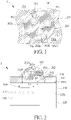
- FIG. 1 is a perspective top view diagram showing a germane portion of an exemplary semiconductor package 1 in accordance with one embodiment of the invention.
- FIG. 2 is a schematic, cross-sectional taken along line I-I' in FIG. 1 .
- the semiconductor package 1 comprises a package substrate 100 having a component side (or chip side) 100a and a board side (or PCB side) 100b.
- the package substrate 100 may be cored substrate with a core layer or a coreless substrate.
- a semiconductor die (or die) 110 may be disposed on the component side 100a of the package substrate 100.
- the semiconductor die 110 is physically and electrically connected to the package substrate 100 through a plurality of connecting elements 111 such as copper pillar, micro-bumps or solder bumps, but not limited thereto.
- the semiconductor die 110 may be over-molded by an encapsulant 120 such as a molding compound comprising epoxy resins.
- the encapsulant 120 is in direct contact with the package substrate 100.
- the semiconductor package 1 may comprise multiple chips or dies in some embodiments. For the sake of simplicity, only a portion of the semiconductor die 110 is shown in the figures.
- the conductive ball pad 102 On the board side 100b of the package substrate 100, at least one conductive ball pad 102 is disposed.
- the conductive ball pad 102 may be located at a corner of the semiconductor package 1. That is, the conductive ball pad 102 may be a corner ball pad disposed adjacent to a vertex of the rectangular shaped semiconductor package 1 when viewed from the bottom of the package 1.
- the conductive ball pad 102 may be a copper pad.
- a surface solderable coating such as a nickel and/or gold coating or an organic solderability preservative (OSP) may be formed on the top surface of the conductive ball pad 102.
- OSP organic solderability preservative
- the conductive ball pad 102 may be electrically connected to a corresponding connecting element 111 through an interconnection structure 104 in the package substrate 100.
- the interconnection structure 104 may comprise copper traces and plated through vias, but not limited thereto.
- the board side 100b of the package substrate 100 and a perimeter of the conductive ball pad 102 may be covered with a solder mask 130.
- the opening 130p of the solder mask 130 partially reveals a central top surface of the conductive ball pad 102.
- the conductive ball pad 102 comprises at least one conductive pillar 202 such as a copper pillar protruding from the top surface of the conductive ball pad 102.
- the height h1 of the conductive pillar 202 above the top surface of the conductive ball pad 102 approximately equals to the height h2 of the solder mask 130 above the top surface of the conductive ball pad 102.
- a top surface 202a of the conductive pillar 202 may be flush with a top surface 130a of the solder mask 130.
- multiple conductive pillars for example, 2 ⁇ 3 pillars (only three exemplary copper pillars are shown in FIG. 1 ), may be disposed on the conductive ball pad 102.
- an extra plating process and a wet etching process are performed.
- an undercut 202s is provided on the sidewall of the conductive pillar 202, thereby forming a curved sidewall profile.
- the undercut 202s may be formed by performing a wet etching process that has faster lateral etching rate, which provides a neck portion 202n that is thinner than its head 202h and base 202b.
- the neck portion 202n may have a smooth, curved surface.
- the base 202b of the conductive pillar 202 may have a width w1 that is greater than a width w2 of the head 202h of the conductive pillar 202.
- the width (or diameter) w2 of the head 202b of the conductive pillar 202 may be about 50 micrometers, but not limited thereto.
- an annular recess 120r may be formed on the conductive ball pad 102 and around the conductive pillar 202.
- a conductive ball 140 such as a solder ball may be disposed on the conductive ball pad 102 and completely surrounds the conductive pillar 202.
- the conductive ball 140, the conductive pillar 202 and the conductive ball pad 102 may be subjected to a reflow process and an inter-metallic compound (IMC) layer (not explicitly shown) may be formed at an interface between the conductive pillar 202 and the conductive ball 140.
- IMC inter-metallic compound
- the conductive pillar 202 and the conductive ball 140 interlock, and the conductive ball 140 is anchored to the conductive ball pad 102.
- the experimental results show that the 3D conductive ball pad 102 with the conductive pillar 202 increases the strength of the solder joint by at least 20%. The conductive ball pad with such conductive pillar 202 can significantly improve the board level reliability.
- only the conductive ball pad at the corner of the semiconductor package 1 has such conductive pillar 202.
- each of the conductive ball pads of the semiconductor package 1 may have such conductive pillar 202.
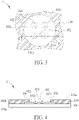
- FIG. 3 demonstrates a schematic top view of a conductive ball pad of an exemplary semiconductor package 2 in accordance with another embodiment of the invention, wherein like layers, regions or elements are designated by like numeral numbers or labels.
- FIG. 4 is a schematic, cross-sectional view taken along line I-I' in FIG. 3 , wherein the detailed structure below the package substrate is omitted in FIG. 4 for the sake of brevity.
- FIG. 5 shows the conductive ball pad of the semiconductor package in FIG. 4 after a conductive ball is mounted on the conductive ball pad.
- FIG. 6 and FIG. 7 show various recessed patterns on the conductive ball pad according to some embodiments.
- recessed regions 102s are provided on the top surface of the conductive ball pad 102.
- the recessed regions 102s are formed by selectively etching predetermined patterns into the top surface 102a of the conductive ball pad 102 using lithographic process and wet or dry etching methods known in the art, thereby forming a protruding feature 302 therebetween.
- each of the recessed regions 102s may have a cross pattern when viewed from the above.
- the recessed regions 102s are isolated from one another by the protruding feature 302.
- the recessed regions 102s may communicate with one another to form a network or interlacing pattern.
- the aerial patterns of the recessed regions 102s are for illustration purposes only. Other patterns such as circular patterns as depicted in FIG. 6 and grid type pattern as depicted in FIG. 7 are also applicable.
- the protruding feature 302 between the recessed regions 102s may have a top surface 302a that is flush with the top surface 102a of the conductive ball pad 102.
- a conductive ball 140 is disposed on the conductive ball pad 102 and completely surrounds the protruding feature 302.
- the recessed regions 102s are filled with the conductive ball 140.
- the conductive ball 140, the protruding feature 302 and the conductive ball pad 102 may be subjected to a reflow process and an inter-metallic compound (IMC) layer (not explicitly shown) may be formed at an interface between the protruding feature 302 and the conductive ball 140.
- IMC inter-metallic compound
- the protruding feature 302 and the conductive ball 140 interlock and the conductive ball 140 is anchored to the conductive ball pad 102.
- FIG. 8 is a perspective top view diagram showing a germane portion of an exemplary semiconductor package 3 in accordance with another embodiment of the invention.
- FIG. 9 is a schematic, cross-sectional taken along line I-I' in FIG. 8 .
- the semiconductor package 3 comprises a package substrate 100 having a component side (or chip side) 100a and a board side (or PCB side) 100b.
- the package substrate 100 may be cored substrate with a core layer or a coreless substrate.
- a semiconductor die (or die) 110 may be disposed on the component side 100a of the package substrate 100.
- the semiconductor die 110 is physically and electrically connected to the package substrate 100 through a plurality of connecting elements 111 such as copper pillar, micro-bumps or solder bumps, but not limited thereto.
- the semiconductor die 110 may be over-molded by an encapsulant 120 such as a molding compound comprising epoxy resins.
- the encapsulant 120 is in direct contact with the package substrate 100.
- the semiconductor package 3 may comprise multiple chips or dies in some embodiments. For the sake of simplicity, only a portion of the semiconductor die 110 is shown in the figures.
- the conductive ball pad 102 On the board side 100b of the package substrate 100, at least one conductive ball pad 102 is disposed.
- the conductive ball pad 102 may be located at a corner of the semiconductor package 3. That is, the conductive ball pad 102 may be a corner ball pad disposed adjacent to a vertex of the rectangular shaped semiconductor package 3 when viewed from the bottom of the package 3.
- the conductive ball pad 102 may be a copper pad.
- a surface solderable coating such as a nickel and/or gold coating or an organic solderability preservative (OSP) may be formed on the top surface of the conductive ball pad 102.
- OSP organic solderability preservative
- the conductive ball pad 102 may be electrically connected to a corresponding connecting element 111 through an interconnection structure 104 in the package substrate 100.
- the interconnection structure 104 may comprise copper traces and plated through vias, but not limited thereto.
- the board side 100b of the package substrate 100 and a perimeter of the conductive ball pad 102 may be covered with a solder mask 130.
- the opening 130p of the solder mask 130 partially reveals a central top surface of the conductive ball pad 102.
- the conductive ball pad 102 comprises at least one conductive pillar 202 such as a copper pillar protruding from the top surface of the conductive ball pad 102.
- the height h1 of the conductive pillar 202 above the top surface of the conductive ball pad 102 approximately equals to the height h2 of the solder mask 130 above the top surface of the conductive ball pad 102.
- a top surface 202a of the conductive pillar 202 may be flush with a top surface 130a of the solder mask 130.
- multiple conductive pillars for example, 2 ⁇ 3 pillars (only three exemplary copper pillars are shown in FIG. 8 ), may be disposed on the conductive ball pad 102.
- an extra plating process and a wet etching process are performed.
- an undercut 202s is provided on the sidewall of the conductive pillar 202, thereby forming a curved sidewall profile.
- the undercut 202s may be formed by performing a wet etching process that has faster lateral etching rate, which provides a neck portion 202n that is thinner than its head 202h and base 202b.
- the neck portion 202n may have a smooth, curved surface.
- the base 202b of the conductive pillar 202 may have a width w1 that is greater than a width w2 of the head 202h of the conductive pillar 202.
- the width (or diameter) w2 of the head 202b of the conductive pillar 202 may be about 50 micrometers, but not limited thereto.
- an annular recess 120r may be formed on the conductive ball pad 102 and around the conductive pillar 202.
- a conductive ball 140 such as a solder ball may be disposed on the conductive ball pad 102 and completely surrounds the conductive pillar 202.
- the conductive ball 140, the conductive pillar 202 and the conductive ball pad 102 may be subjected to a reflow process and an inter-metallic compound (IMC) layer (not explicitly shown) may be formed at an interface between the conductive pillar 202 and the conductive ball 140.
- IMC inter-metallic compound
- the conductive pillar 202 and the conductive ball 140 interlock, and the conductive ball 140 is anchored to the conductive ball pad 102.
- recessed regions 102r are provided on the top surface of the conductive ball pad 102 and around the conductive pillar 202.
- the recessed regions 102r are formed by selectively etching predetermined patterns into the top surface 102a of the conductive ball pad 102 using lithographic process and wet or dry etching methods known in the art.
Landscapes
- Electric Connection Of Electric Components To Printed Circuits (AREA)
- Internal Circuitry In Semiconductor Integrated Circuit Devices (AREA)
- Physics & Mathematics (AREA)
- Geometry (AREA)
- Wire Bonding (AREA)
Abstract
A three-dimensional pad structure includes a substrate (100); a pad (102) disposed on the substrate (100), wherein a perimeter of the pad (102) is covered with a solder mask (130); and at least one conductive pillar (202) protruding from a top surface of the pad (102).
Description
- This application claims priorities from
U.S. provisional application No. 63/171,637 filed on April 7, 2021 - The present disclosure relates generally to an improved conductive ball pad and an interconnection structure for electronic components or devices.
- Ball grid array (BGA) packages are rapidly gaining acceptance in the electronics industry as a low-cost, higher yielding alternative to fine pitch leaded packages. Conductive solder joints are formed to mechanically and electrically interconnect the pads on the component/device with the corresponding pads on the substrate. Whether structural or electronic, all solder joints must provide the necessary level of reliability for the application.
- As known in the art, the inter-metallic compound (IMC) layer is the key to form the good soldering but it is also the weakest layer in the whole soldering structure. The IMC layer with poor mechanical strength is damaged easily during undergoing process mechanical stress, even though process strain level is within design specification.
- It is desired to provide an improved interconnection structure that is capable of solving the crack phenomenon on current printed circuit board assembly (PCBA) without changing any BGA produced process.
- One object of the present invention is to provide a three-dimensional conductive ball pad, an improved interconnection structure, and semiconductor package using the same, in order to solve the above-mentioned prior art problems or shortcomings. Three-dimensional pad structures according to the invention are defined in the independent claims. The dependent claims define preferred embodiments thereof.
- One aspect of the disclosure provides a three-dimensional pad structure including a substrate; a pad disposed on the substrate, wherein a perimeter of the pad is covered with a solder mask; and at least one conductive pillar protruding from a top surface of the pad.
- Preferably, the substrate is a package substrate having a component side and a board side, wherein the pad is disposed on the board side of the package substrate.
- Preferably, the pad is a copper pad.
- Preferably, the at least one conductive pillar is a copper pillar.
- Preferably, a height of the conductive pillar above the top surface of the pad approximately equals to a height of the solder mask above the top surface of the pad.
- Preferably, the three-dimensional pad structure further comprises a surface solderable coating or an organic solderability preservative (OSP) on the top surface of the pad.
- Preferably, a top surface of the conductive pillar is flush with a top surface of the solder mask.
- Preferably, an undercut is provided on a sidewall of the conductive pillar, thereby constituting a curved sidewall profile.
- Preferably, the conductive pillar comprises a neck portion that is thinner than its head and base.
- Preferably, the neck portion has a smooth, curved surface.
- Preferably, a width of the head of the conductive pillar is about 50 micrometers.
- Preferably, the three-dimensional pad structure further comprises an annular recess on the pad and around the conductive pillar.
- Another aspect of the disclosure provides an interconnection structure including a substrate; a pad disposed on the substrate, wherein a perimeter of the pad is covered with a solder mask; at least one conductive pillar protruding from a top surface of the pad; and a conductive ball disposed on the pad and surrounds the conductive pillar, wherein the at least one conductive pillar and the conductive ball interlock, and wherein the conductive ball is anchored to the pad.
- Preferably, conductive ball completely surrounds the conductive pillar.
- Preferably, the substrate is a package substrate having a component side and a board side, wherein the pad is disposed on the board side of the package substrate.
- Preferably, the pad is a copper pad.
- Preferably, the at least one conductive pillar is a copper pillar.
- Preferably, the interconnection structure further comprises a surface solderable coating or an organic solderability preservative (OSP) on the top surface of the pad.
- Preferably, an undercut is provided on a sidewall of the conductive pillar, thereby constituting a curved sidewall profile.
- Preferably, the conductive pillar comprises a neck portion that is thinner than its head and base.
- Preferably, the neck portion has a smooth, curved surface.
- Preferably, a width of the head of the conductive pillar is about 50 micrometers.
- Preferably, the interconnection structure further comprises an annular recess on the pad and around the conductive pillar.
- Preferably, the pad is a corner pad.
- Still another aspect of the disclosure provides a three-dimensional pad structure including a substrate; a pad disposed on the substrate, wherein a perimeter of the pad is covered with a solder mask; and recessed regions provided on a top surface of the pad; and at least one protruding feature between the recessed regions.
- Preferably, the recessed regions are isolated from one another by the protruding feature.
- Preferably, the recessed regions communicate with one another to form a network or interlacing pattern.
- Preferably, the protruding feature between the recessed regions has a top surface that is flush with the top surface of the pad.
- Preferably, the substrate is a package substrate having a component side and a board side, wherein the pad is disposed on the board side of the package substrate.
- Preferably, the pad is a copper pad.
- The interconnection structure according to the present invention comprises in particular one or both of the three-dimensional pad structures according to the present invention. These and other objectives of the present invention will no doubt become obvious to those of ordinary skill in the art after reading the following detailed description of the preferred embodiment that is illustrated in the various figures and drawings.
- The accompanying drawings are included to provide a further understanding of the invention and are incorporated in and constitute a part of this specification. The drawings illustrate embodiments of the invention and, together with the description, serve to explain the principles of the invention. In the drawings:
-
FIG. 1 is a perspective top view diagram showing a germane portion of an exemplary semiconductor package in accordance with one embodiment of the invention; -
FIG. 2 is a schematic, cross-sectional taken along line I-I' inFIG. 1 ; -
FIG. 3 demonstrates a schematic, top view of a conductive ball pad of an exemplary semiconductor package in accordance with another embodiment of the invention; -
FIG. 4 is a schematic, cross-sectional view taken along line I-I' inFIG. 3 ; -
FIG. 5 shows the conductive ball pad of the semiconductor package inFIG. 4 after a conductive ball is mounted on the conductive ball pad; -
FIG. 6 andFIG. 7 show various recessed patterns on the conductive ball pad according to some embodiments; and -
FIG. 8 is a perspective top view diagram showing a germane portion of an exemplary semiconductor package in accordance with another embodiment of the invention; and -
FIG. 9 is a schematic, cross-sectional taken along line I-I' inFIG. 8 . - In the following detailed description of embodiments of the invention, reference is made to the accompanying drawings, which form a part hereof, and in which is shown by way of illustration specific preferred embodiments in which the disclosure may be practiced.
- These embodiments are described in sufficient detail to enable those skilled in the art to practice them, and it is to be understood that other embodiments may be utilized and that mechanical, chemical, electrical, and procedural changes may be made without departing from the scope of the present disclosure. The following detailed description is, therefore, not to be taken in a limiting sense, and the scope of embodiments of the present invention is defined only by the appended claims.
- It will be understood that when an element or layer is referred to as being "on", "connected to" or "coupled to" another element or layer, it can be directly on, connected or coupled to the other element or layer or intervening elements or layers may be present. In contrast, when an element is referred to as being "directly on," "directly connected to" or "directly coupled to" another element or layer, there are no intervening elements or layers present. Like numbers refer to like elements throughout. As used herein, the term "and/or" includes any and all combinations of one or more of the associated listed items.
- In ball grid array (BGA) packages, instead of a lead frame, an organic substrate is typically used. The substrate is generally made of bismaleimide triazine or polyimide. The chip is mounted to the top of the substrate, and conductive balls constructed on the bottom of the substrate make connections to the circuit board. This design allows for shorter circuit interconnect lengths, which improve electrical performance, as well as a smaller package size. In the BGA packaging, the integrated circuit (IC) component, solder joints and printed circuit board (PCB) form a three-layer construction.
- Drop induced interconnect failure is a major reliability concern for portable electronic applications. Failure typically occurs at package/solder interface at corner BGA balls, which results in lower I/O density because corner BGA balls are not I/O balls in consideration of board level reliability (BLR) concern. BLR has been the one of the critical issue for using BGA packages in automotive. The required specification of BLR is listed in various standards (AEC-Q100, Q104, etc.) and it is varied by automotive application customers.
- The present disclosure pertains to a novel three-dimensional (3D) conductive ball pad for mechanical and electrical interconnection between opposing electrodes of electronic components/devices, functional modules, and substrates, and an interconnection structure formed with conductive joint and the 3D conductive ball pad.
- Please refer to
FIG. 1 and FIG. 2. FIG. 1 is a perspective top view diagram showing a germane portion of anexemplary semiconductor package 1 in accordance with one embodiment of the invention.FIG. 2 is a schematic, cross-sectional taken along line I-I' inFIG. 1 . As shown inFIG. 1 and FIG. 2 , thesemiconductor package 1 comprises apackage substrate 100 having a component side (or chip side) 100a and a board side (or PCB side) 100b. Thepackage substrate 100 may be cored substrate with a core layer or a coreless substrate. According to an embodiment, a semiconductor die (or die) 110 may be disposed on thecomponent side 100a of thepackage substrate 100. The semiconductor die 110 is physically and electrically connected to thepackage substrate 100 through a plurality of connectingelements 111 such as copper pillar, micro-bumps or solder bumps, but not limited thereto. - According to an embodiment, the semiconductor die 110 may be over-molded by an
encapsulant 120 such as a molding compound comprising epoxy resins. Theencapsulant 120 is in direct contact with thepackage substrate 100. It is understood that thesemiconductor package 1 may comprise multiple chips or dies in some embodiments. For the sake of simplicity, only a portion of the semiconductor die 110 is shown in the figures. - On the
board side 100b of thepackage substrate 100, at least oneconductive ball pad 102 is disposed. According to an embodiment, for example, theconductive ball pad 102 may be located at a corner of thesemiconductor package 1. That is, theconductive ball pad 102 may be a corner ball pad disposed adjacent to a vertex of the rectangular shapedsemiconductor package 1 when viewed from the bottom of thepackage 1. According to an embodiment, for example, theconductive ball pad 102 may be a copper pad. Depending upon design requirements, a surface solderable coating such as a nickel and/or gold coating or an organic solderability preservative (OSP) may be formed on the top surface of theconductive ball pad 102. According to an embodiment, theconductive ball pad 102 may be electrically connected to a corresponding connectingelement 111 through aninterconnection structure 104 in thepackage substrate 100. For example, theinterconnection structure 104 may comprise copper traces and plated through vias, but not limited thereto. - According to an embodiment, the
board side 100b of thepackage substrate 100 and a perimeter of theconductive ball pad 102 may be covered with asolder mask 130. Theopening 130p of thesolder mask 130 partially reveals a central top surface of theconductive ball pad 102. According to an embodiment, theconductive ball pad 102 comprises at least oneconductive pillar 202 such as a copper pillar protruding from the top surface of theconductive ball pad 102. For example, the height h1 of theconductive pillar 202 above the top surface of theconductive ball pad 102 approximately equals to the height h2 of thesolder mask 130 above the top surface of theconductive ball pad 102. According to an embodiment, atop surface 202a of theconductive pillar 202 may be flush with atop surface 130a of thesolder mask 130. In some embodiment, multiple conductive pillars, for example, 2~3 pillars (only three exemplary copper pillars are shown inFIG. 1 ), may be disposed on theconductive ball pad 102. According to an embodiment, to form theconductive pillar 202, an extra plating process and a wet etching process are performed. - According to an embodiment, as cane be seen in
FIG. 2 , an undercut 202s is provided on the sidewall of theconductive pillar 202, thereby forming a curved sidewall profile. The undercut 202s may be formed by performing a wet etching process that has faster lateral etching rate, which provides aneck portion 202n that is thinner than itshead 202h andbase 202b. According to an embodiment, theneck portion 202n may have a smooth, curved surface. According to an embodiment, thebase 202b of theconductive pillar 202 may have a width w1 that is greater than a width w2 of thehead 202h of theconductive pillar 202. For example, the width (or diameter) w2 of thehead 202b of theconductive pillar 202 may be about 50 micrometers, but not limited thereto. After the wet etching process is completed, an annular recess 120r may be formed on theconductive ball pad 102 and around theconductive pillar 202. - According to an embodiment, a
conductive ball 140 such as a solder ball may be disposed on theconductive ball pad 102 and completely surrounds theconductive pillar 202. According to an embodiment, theconductive ball 140, theconductive pillar 202 and theconductive ball pad 102 may be subjected to a reflow process and an inter-metallic compound (IMC) layer (not explicitly shown) may be formed at an interface between theconductive pillar 202 and theconductive ball 140. According to an embodiment, theconductive pillar 202 and theconductive ball 140 interlock, and theconductive ball 140 is anchored to theconductive ball pad 102. The experimental results show that the 3Dconductive ball pad 102 with theconductive pillar 202 increases the strength of the solder joint by at least 20%. The conductive ball pad with suchconductive pillar 202 can significantly improve the board level reliability. - According to an embodiment, only the conductive ball pad at the corner of the
semiconductor package 1 has suchconductive pillar 202. Preferably, each of the conductive ball pads of thesemiconductor package 1 may have suchconductive pillar 202. - Please refer to
FIG. 3 to FIG. 7 .FIG. 3 demonstrates a schematic top view of a conductive ball pad of anexemplary semiconductor package 2 in accordance with another embodiment of the invention, wherein like layers, regions or elements are designated by like numeral numbers or labels.FIG. 4 is a schematic, cross-sectional view taken along line I-I' inFIG. 3 , wherein the detailed structure below the package substrate is omitted inFIG. 4 for the sake of brevity.FIG. 5 shows the conductive ball pad of the semiconductor package inFIG. 4 after a conductive ball is mounted on the conductive ball pad.FIG. 6 andFIG. 7 show various recessed patterns on the conductive ball pad according to some embodiments. - As shown in
FIG. 3 and FIG. 4 , recessedregions 102s are provided on the top surface of theconductive ball pad 102. The recessedregions 102s are formed by selectively etching predetermined patterns into thetop surface 102a of theconductive ball pad 102 using lithographic process and wet or dry etching methods known in the art, thereby forming aprotruding feature 302 therebetween. For example, each of the recessedregions 102s may have a cross pattern when viewed from the above. According to an embodiment, the recessedregions 102s are isolated from one another by theprotruding feature 302. In some embodiments, the recessedregions 102s may communicate with one another to form a network or interlacing pattern. - It is understood that the aerial patterns of the recessed
regions 102s are for illustration purposes only. Other patterns such as circular patterns as depicted inFIG. 6 and grid type pattern as depicted inFIG. 7 are also applicable. Theprotruding feature 302 between the recessedregions 102s may have atop surface 302a that is flush with thetop surface 102a of theconductive ball pad 102. - According to an embodiment, as shown in
FIG. 6 , likewise, aconductive ball 140 is disposed on theconductive ball pad 102 and completely surrounds theprotruding feature 302. The recessedregions 102s are filled with theconductive ball 140. According to an embodiment, theconductive ball 140, the protrudingfeature 302 and theconductive ball pad 102 may be subjected to a reflow process and an inter-metallic compound (IMC) layer (not explicitly shown) may be formed at an interface between theprotruding feature 302 and theconductive ball 140. According to an embodiment, the protrudingfeature 302 and theconductive ball 140 interlock and theconductive ball 140 is anchored to theconductive ball pad 102. - Please refer to
FIG. 8 andFIG. 9 .FIG. 8 is a perspective top view diagram showing a germane portion of anexemplary semiconductor package 3 in accordance with another embodiment of the invention.FIG. 9 is a schematic, cross-sectional taken along line I-I' inFIG. 8 . As shown inFIG. 8 andFIG. 9 , likewise, thesemiconductor package 3 comprises apackage substrate 100 having a component side (or chip side) 100a and a board side (or PCB side) 100b. Thepackage substrate 100 may be cored substrate with a core layer or a coreless substrate. According to an embodiment, a semiconductor die (or die) 110 may be disposed on thecomponent side 100a of thepackage substrate 100. The semiconductor die 110 is physically and electrically connected to thepackage substrate 100 through a plurality of connectingelements 111 such as copper pillar, micro-bumps or solder bumps, but not limited thereto. - According to an embodiment, the semiconductor die 110 may be over-molded by an
encapsulant 120 such as a molding compound comprising epoxy resins. Theencapsulant 120 is in direct contact with thepackage substrate 100. It is understood that thesemiconductor package 3 may comprise multiple chips or dies in some embodiments. For the sake of simplicity, only a portion of the semiconductor die 110 is shown in the figures. - On the
board side 100b of thepackage substrate 100, at least oneconductive ball pad 102 is disposed. According to an embodiment, for example, theconductive ball pad 102 may be located at a corner of thesemiconductor package 3. That is, theconductive ball pad 102 may be a corner ball pad disposed adjacent to a vertex of the rectangular shapedsemiconductor package 3 when viewed from the bottom of thepackage 3. According to an embodiment, for example, theconductive ball pad 102 may be a copper pad. Depending upon design requirements, a surface solderable coating such as a nickel and/or gold coating or an organic solderability preservative (OSP) may be formed on the top surface of theconductive ball pad 102. According to an embodiment, theconductive ball pad 102 may be electrically connected to a corresponding connectingelement 111 through aninterconnection structure 104 in thepackage substrate 100. For example, theinterconnection structure 104 may comprise copper traces and plated through vias, but not limited thereto. - According to an embodiment, the
board side 100b of thepackage substrate 100 and a perimeter of theconductive ball pad 102 may be covered with asolder mask 130. Theopening 130p of thesolder mask 130 partially reveals a central top surface of theconductive ball pad 102. According to an embodiment, theconductive ball pad 102 comprises at least oneconductive pillar 202 such as a copper pillar protruding from the top surface of theconductive ball pad 102. For example, the height h1 of theconductive pillar 202 above the top surface of theconductive ball pad 102 approximately equals to the height h2 of thesolder mask 130 above the top surface of theconductive ball pad 102. According to an embodiment, atop surface 202a of theconductive pillar 202 may be flush with atop surface 130a of thesolder mask 130. In some embodiment, multiple conductive pillars, for example, 2~3 pillars (only three exemplary copper pillars are shown inFIG. 8 ), may be disposed on theconductive ball pad 102. According to an embodiment, to form theconductive pillar 202, an extra plating process and a wet etching process are performed. - According to an embodiment, as cane be seen in
FIG. 9 , an undercut 202s is provided on the sidewall of theconductive pillar 202, thereby forming a curved sidewall profile. The undercut 202s may be formed by performing a wet etching process that has faster lateral etching rate, which provides aneck portion 202n that is thinner than itshead 202h andbase 202b. According to an embodiment, theneck portion 202n may have a smooth, curved surface. According to an embodiment, thebase 202b of theconductive pillar 202 may have a width w1 that is greater than a width w2 of thehead 202h of theconductive pillar 202. For example, the width (or diameter) w2 of thehead 202b of theconductive pillar 202 may be about 50 micrometers, but not limited thereto. After the wet etching process is completed, an annular recess 120r may be formed on theconductive ball pad 102 and around theconductive pillar 202. - According to an embodiment, a
conductive ball 140 such as a solder ball may be disposed on theconductive ball pad 102 and completely surrounds theconductive pillar 202. According to an embodiment, theconductive ball 140, theconductive pillar 202 and theconductive ball pad 102 may be subjected to a reflow process and an inter-metallic compound (IMC) layer (not explicitly shown) may be formed at an interface between theconductive pillar 202 and theconductive ball 140. According to an embodiment, theconductive pillar 202 and theconductive ball 140 interlock, and theconductive ball 140 is anchored to theconductive ball pad 102. - According to an embodiment, recessed
regions 102r are provided on the top surface of theconductive ball pad 102 and around theconductive pillar 202. The recessedregions 102r are formed by selectively etching predetermined patterns into thetop surface 102a of theconductive ball pad 102 using lithographic process and wet or dry etching methods known in the art. - Those skilled in the art will readily observe that numerous modifications and alterations of the device and method may be made while retaining the teachings of the invention. Accordingly, the above disclosure should be construed as limited only by the metes and bounds of the appended claims.
Claims (15)
- A three-dimensional pad structure, comprising:a substrate (100);a pad (102) disposed on the substrate (100), wherein a perimeter of the pad (102) is covered with a solder mask (130); andat least one conductive pillar (202) protruding from a top surface of the pad (102).
- The three-dimensional pad structure according to claim 1, wherein each of the at least one conductive pillar (202) is a copper pillar.
- The three-dimensional pad structure according to claim 1 or 2, wherein a height (h1) of each of the at least one conductive pillar (202) above the top surface of the pad (102) approximately equals to a height (h2) of the solder mask (130) above the top surface of the pad (102).
- The three-dimensional pad structure according to any one of claims 1 to 3, further comprising:
a surface solderable coating or an organic solderability preservative, also referred to as OSP, on the top surface of the pad (102). - The three-dimensional pad structure according to any one of claims 1 to 4, wherein a top surface (202a) of each of the at least one conductive pillar (202) is flush with a top surface (130a) of the solder mask (130).
- The three-dimensional pad structure according to any one of claims 1 to 5, wherein an undercut (202s) is provided on a sidewall of each of the at least one conductive pillar (202), thereby constituting a curved sidewall profile.
- The three-dimensional pad structure according to any one of claims 1 to 6, wherein each of the at least one conductive pillar (202) comprises a neck portion (202n) that is thinner than its head (202h) and base (202b).
- The three-dimensional pad structure according to claim 7, wherein the neck portion (202n) has a smooth, curved surface; and/or
wherein a width (w2) of the head (202h) of each of the at least one conductive pillar (202) is about 50 micrometers. - The three-dimensional pad structure according to any one of claims 1 to 8, further comprising:
an annular recess (120r) on the pad (102) and around the at least one conductive pillar (202). - A three-dimensional pad structure, comprising:a substrate (100);a pad (102) disposed on the substrate (100), wherein a perimeter of the pad (102) is covered with a solder mask (130); andrecessed regions (102s) provided on a top surface of the pad (102); andat least one protruding feature (302) between the recessed regions (102s).
- The three-dimensional pad structure according to claim 10, wherein the recessed regions (102s) are isolated from one another by the at least one protruding feature (302); and/or
wherein the recessed regions (102s) communicate with one another to form a network or interlacing pattern. - The three-dimensional pad structure according to claim 10 or 11, wherein each of the at least one protruding feature (302) between the recessed regions (102s) has a top surface (302a) that is flush with the top surface (102a) of the pad (102).
- The three-dimensional pad structure according to any one of claims 1 to 12, wherein the substrate (100) is a package substrate having a component side (100a) and a board side (100b),wherein the pad (102) is disposed on the board side (100b) of the package substrate (100); and/orwherein the pad (102) is a copper pad; and/orwherein the pad (102) is a corner pad.
- An interconnection structure, comprising:a three-dimensional pad structure according to any one of the preceding claims; anda conductive ball (140) disposed on the pad (102) and surrounding the at least one conductive pillar (202) or the at least one protruding feature (302), wherein each of the at least one conductive pillar (202) or the at least one protruding feature (302) and the conductive ball (140) interlock, and wherein the conductive ball (140) is anchored to the pad (102).
- The interconnection structure according to claim 14, wherein conductive ball (140) completely surrounds the at least one conductive pillar (202) or the at least one protruding feature (302).
Applications Claiming Priority (2)
| Application Number | Priority Date | Filing Date | Title |
|---|---|---|---|
| US202163171637P | 2021-04-07 | 2021-04-07 | |
| US17/691,056 US12230562B2 (en) | 2021-04-07 | 2022-03-09 | Three-dimensional pad structure and interconnection structure for electronic devices |
Publications (1)
| Publication Number | Publication Date |
|---|---|
| EP4071792A1 true EP4071792A1 (en) | 2022-10-12 |
Family
ID=81386720
Family Applications (1)
| Application Number | Title | Priority Date | Filing Date |
|---|---|---|---|
| EP22164134.3A Withdrawn EP4071792A1 (en) | 2021-04-07 | 2022-03-24 | Three-dimensional pad structure and interconnection structure for electronic devices |
Country Status (4)
| Country | Link |
|---|---|
| US (1) | US12230562B2 (en) |
| EP (1) | EP4071792A1 (en) |
| CN (1) | CN115206915A (en) |
| TW (1) | TWI815356B (en) |
Families Citing this family (1)
| Publication number | Priority date | Publication date | Assignee | Title |
|---|---|---|---|---|
| US12230562B2 (en) * | 2021-04-07 | 2025-02-18 | Mediatek Inc. | Three-dimensional pad structure and interconnection structure for electronic devices |
Citations (8)
| Publication number | Priority date | Publication date | Assignee | Title |
|---|---|---|---|---|
| JP2000164617A (en) * | 1998-11-25 | 2000-06-16 | Sanyo Electric Co Ltd | Chip size package and manufacturing method thereof |
| US20100044884A1 (en) * | 2008-08-19 | 2010-02-25 | Ati Technologies Ulc | Integrated circuit package employing predetermined three-dimensional solder pad surface and method for making same |
| US7700475B1 (en) * | 2006-10-05 | 2010-04-20 | Marvell International Ltd. | Pillar structure on bump pad |
| US20120306104A1 (en) * | 2011-05-31 | 2012-12-06 | Stats Chippac, Ltd. | Semiconductor Device and Method of Forming Interconnect Structure With Conductive Pads Having Expanded Interconnect Surface Area for Enhanced Interconnection Properties |
| JP2014192177A (en) * | 2013-03-26 | 2014-10-06 | Ngk Spark Plug Co Ltd | Wiring board |
| WO2014199890A1 (en) * | 2013-06-14 | 2014-12-18 | 三菱製紙株式会社 | Method for manufacturing wiring board |
| US20150333022A1 (en) * | 2014-05-16 | 2015-11-19 | Sven Albers | Contact pads for integrated circuit packages |
| US20200118955A1 (en) * | 2018-10-11 | 2020-04-16 | Intel Corporation | Pad design for thermal fatigue resistance and interconnect joint reliability |
Family Cites Families (59)
| Publication number | Priority date | Publication date | Assignee | Title |
|---|---|---|---|---|
| US5788143A (en) * | 1992-04-08 | 1998-08-04 | International Business Machines Corporation | Solder particle deposition |
| JPH08115989A (en) * | 1994-08-24 | 1996-05-07 | Fujitsu Ltd | Semiconductor device and manufacturing method thereof |
| JPH10294418A (en) * | 1997-04-21 | 1998-11-04 | Oki Electric Ind Co Ltd | Semiconductor device |
| US5869889A (en) * | 1997-04-21 | 1999-02-09 | Lsi Logic Corporation | Thin power tape ball grid array package |
| JP3068534B2 (en) * | 1997-10-14 | 2000-07-24 | 九州日本電気株式会社 | Semiconductor device |
| US6214716B1 (en) * | 1998-09-30 | 2001-04-10 | Micron Technology, Inc. | Semiconductor substrate-based BGA interconnection and methods of farication same |
| JP3416545B2 (en) * | 1998-12-10 | 2003-06-16 | 三洋電機株式会社 | Chip size package and manufacturing method thereof |
| JP2001223293A (en) * | 2000-02-09 | 2001-08-17 | Nec Corp | Semiconductor device and manufacturing method thereof |
| US6403460B1 (en) * | 2000-08-22 | 2002-06-11 | Charles W. C. Lin | Method of making a semiconductor chip assembly |
| US6511865B1 (en) * | 2000-09-20 | 2003-01-28 | Charles W. C. Lin | Method for forming a ball bond connection joint on a conductive trace and conductive pad in a semiconductor chip assembly |
| US6350632B1 (en) * | 2000-09-20 | 2002-02-26 | Charles W. C. Lin | Semiconductor chip assembly with ball bond connection joint |
| US7129113B1 (en) * | 2000-10-13 | 2006-10-31 | Bridge Semiconductor Corporation | Method of making a three-dimensional stacked semiconductor package with a metal pillar in an encapsulant aperture |
| US7319265B1 (en) * | 2000-10-13 | 2008-01-15 | Bridge Semiconductor Corporation | Semiconductor chip assembly with precision-formed metal pillar |
| US7414319B2 (en) * | 2000-10-13 | 2008-08-19 | Bridge Semiconductor Corporation | Semiconductor chip assembly with metal containment wall and solder terminal |
| US7262082B1 (en) * | 2000-10-13 | 2007-08-28 | Bridge Semiconductor Corporation | Method of making a three-dimensional stacked semiconductor package with a metal pillar and a conductive interconnect in an encapsulant aperture |
| US6576539B1 (en) * | 2000-10-13 | 2003-06-10 | Charles W.C. Lin | Semiconductor chip assembly with interlocked conductive trace |
| US7075186B1 (en) * | 2000-10-13 | 2006-07-11 | Bridge Semiconductor Corporation | Semiconductor chip assembly with interlocked contact terminal |
| US7242099B2 (en) * | 2001-03-05 | 2007-07-10 | Megica Corporation | Chip package with multiple chips connected by bumps |
| US7902679B2 (en) * | 2001-03-05 | 2011-03-08 | Megica Corporation | Structure and manufacturing method of a chip scale package with low fabrication cost, fine pitch and high reliability solder bump |
| TWI313507B (en) * | 2002-10-25 | 2009-08-11 | Megica Corporatio | Method for assembling chips |
| US6818545B2 (en) * | 2001-03-05 | 2004-11-16 | Megic Corporation | Low fabrication cost, fine pitch and high reliability solder bump |
| US7241640B1 (en) * | 2005-02-08 | 2007-07-10 | Xilinx, Inc. | Solder ball assembly for a semiconductor device and method of fabricating same |
| US7939934B2 (en) * | 2005-03-16 | 2011-05-10 | Tessera, Inc. | Microelectronic packages and methods therefor |
| DE102005014665A1 (en) * | 2005-03-29 | 2006-11-02 | Infineon Technologies Ag | Substrate for producing a solder joint with a second substrate |
| KR100664500B1 (en) * | 2005-08-09 | 2007-01-04 | 삼성전자주식회사 | Printed circuit board having a metal land having a protrusion and a manufacturing method thereof |
| US7361531B2 (en) * | 2005-11-01 | 2008-04-22 | Allegro Microsystems, Inc. | Methods and apparatus for Flip-Chip-On-Lead semiconductor package |
| US7919868B2 (en) * | 2007-08-15 | 2011-04-05 | Qimonda Ag | Carrier substrate and integrated circuit |
| US20090174069A1 (en) * | 2008-01-04 | 2009-07-09 | National Semiconductor Corporation | I/o pad structure for enhancing solder joint reliability in integrated circuit devices |
| US20090243100A1 (en) * | 2008-03-27 | 2009-10-01 | Jotaro Akiyama | Methods to Form a Three-Dimensionally Curved Pad in a Substrate and Integrated Circuits Incorporating such a Substrate |
| US9093767B2 (en) * | 2009-06-02 | 2015-07-28 | Hsio Technologies, Llc | High performance surface mount electrical interconnect |
| US8115310B2 (en) * | 2009-06-11 | 2012-02-14 | Texas Instruments Incorporated | Copper pillar bonding for fine pitch flip chip devices |
| US8315063B2 (en) * | 2009-08-26 | 2012-11-20 | Kinsus Interconnect Technology Corp. | Solder pad structure with high bondability to solder ball |
| US20110227216A1 (en) * | 2010-03-16 | 2011-09-22 | Taiwan Semiconductor Manufacturing Company, Ltd. | Under-Bump Metallization Structure for Semiconductor Devices |
| US10159154B2 (en) * | 2010-06-03 | 2018-12-18 | Hsio Technologies, Llc | Fusion bonded liquid crystal polymer circuit structure |
| US8884432B2 (en) * | 2011-06-08 | 2014-11-11 | Tessera, Inc. | Substrate and assembly thereof with dielectric removal for increased post height |
| KR101847162B1 (en) * | 2011-09-27 | 2018-05-29 | 삼성전기주식회사 | Semiconductor package and method for manufacturing the same |
| US9165875B2 (en) * | 2012-04-25 | 2015-10-20 | Taiwan Semiconductor Manufacturing Company, Ltd. | Low profile interposer with stud structure |
| JP2013236039A (en) * | 2012-05-11 | 2013-11-21 | Renesas Electronics Corp | Semiconductor device |
| US9761520B2 (en) * | 2012-07-10 | 2017-09-12 | Hsio Technologies, Llc | Method of making an electrical connector having electrodeposited terminals |
| US8659153B2 (en) * | 2012-07-16 | 2014-02-25 | Micron Technology, Inc. | Pillar on pad interconnect structures, semiconductor dice and die assemblies including such interconnect structures, and related methods |
| US10667410B2 (en) * | 2013-07-11 | 2020-05-26 | Hsio Technologies, Llc | Method of making a fusion bonded circuit structure |
| US9355979B2 (en) * | 2013-08-16 | 2016-05-31 | Taiwan Semiconductor Manufacturing Company, Ltd. | Alignment structures and methods of forming same |
| US9165877B2 (en) * | 2013-10-04 | 2015-10-20 | Mediatek Inc. | Fan-out semiconductor package with copper pillar bumps |
| KR102134019B1 (en) * | 2013-11-25 | 2020-07-14 | 에스케이하이닉스 주식회사 | Substrate and semiconductor package having ball land, and the methods of fabricating the same |
| US20150340308A1 (en) * | 2014-05-21 | 2015-11-26 | Broadcom Corporation | Reconstituted interposer semiconductor package |
| US20160079205A1 (en) * | 2014-09-15 | 2016-03-17 | Mediatek Inc. | Semiconductor package assembly |
| MY192389A (en) * | 2016-07-01 | 2022-08-18 | Intel Corp | Systems, methods, and apparatuses for implementing a pad on solder mask (posm) semiconductor substrate package |
| US9984960B2 (en) * | 2016-07-21 | 2018-05-29 | Taiwan Semiconductor Manufacturing Co., Ltd. | Integrated fan-out package and method of fabricating the same |
| US20180053665A1 (en) * | 2016-08-19 | 2018-02-22 | Mediatek Inc. | Pre-bumped redistribution layer structure and semiconductor package incorporating such pre-bumped redistribution layer structure |
| US10756040B2 (en) * | 2017-02-13 | 2020-08-25 | Mediatek Inc. | Semiconductor package with rigid under bump metallurgy (UBM) stack |
| US10269672B2 (en) * | 2017-08-24 | 2019-04-23 | Advanced Semiconductor Engineering, Inc. | Semiconductor package device and method of manufacturing the same |
| US10276479B1 (en) * | 2017-10-11 | 2019-04-30 | Micron Technology, Inc. | Methods of processing semiconductor devices |
| US10716213B2 (en) * | 2018-07-28 | 2020-07-14 | Hewlett Packard Enterprise Development Lp | Direct connection of high speed signals on PCB chip |
| US10825773B2 (en) * | 2018-09-27 | 2020-11-03 | Taiwan Semiconductor Manufacturing Co., Ltd. | Package structure with reinforcement structures in a redistribution circuit structure and method of manufacturing the same |
| US11063019B2 (en) * | 2019-07-17 | 2021-07-13 | Taiwan Semiconductor Manufacturing Company, Ltd. | Package structure, chip structure and method of fabricating the same |
| US11233024B2 (en) * | 2019-12-23 | 2022-01-25 | Micron Technology, Inc. | Methods for forming substrate terminal pads, related terminal pads and substrates and assemblies incorporating such terminal pads |
| CN111199889B (en) * | 2020-01-10 | 2021-07-16 | 宝德照明集团有限公司 | A kind of semiconductor packaging structure and preparation method thereof |
| US20220165694A1 (en) * | 2020-11-26 | 2022-05-26 | Mediatek Inc. | Semiconductor structure |
| US12230562B2 (en) * | 2021-04-07 | 2025-02-18 | Mediatek Inc. | Three-dimensional pad structure and interconnection structure for electronic devices |
-
2022
- 2022-03-09 US US17/691,056 patent/US12230562B2/en active Active
- 2022-03-17 TW TW111109768A patent/TWI815356B/en active
- 2022-03-22 CN CN202210289173.4A patent/CN115206915A/en active Pending
- 2022-03-24 EP EP22164134.3A patent/EP4071792A1/en not_active Withdrawn
Patent Citations (8)
| Publication number | Priority date | Publication date | Assignee | Title |
|---|---|---|---|---|
| JP2000164617A (en) * | 1998-11-25 | 2000-06-16 | Sanyo Electric Co Ltd | Chip size package and manufacturing method thereof |
| US7700475B1 (en) * | 2006-10-05 | 2010-04-20 | Marvell International Ltd. | Pillar structure on bump pad |
| US20100044884A1 (en) * | 2008-08-19 | 2010-02-25 | Ati Technologies Ulc | Integrated circuit package employing predetermined three-dimensional solder pad surface and method for making same |
| US20120306104A1 (en) * | 2011-05-31 | 2012-12-06 | Stats Chippac, Ltd. | Semiconductor Device and Method of Forming Interconnect Structure With Conductive Pads Having Expanded Interconnect Surface Area for Enhanced Interconnection Properties |
| JP2014192177A (en) * | 2013-03-26 | 2014-10-06 | Ngk Spark Plug Co Ltd | Wiring board |
| WO2014199890A1 (en) * | 2013-06-14 | 2014-12-18 | 三菱製紙株式会社 | Method for manufacturing wiring board |
| US20150333022A1 (en) * | 2014-05-16 | 2015-11-19 | Sven Albers | Contact pads for integrated circuit packages |
| US20200118955A1 (en) * | 2018-10-11 | 2020-04-16 | Intel Corporation | Pad design for thermal fatigue resistance and interconnect joint reliability |
Also Published As
| Publication number | Publication date |
|---|---|
| US20220328394A1 (en) | 2022-10-13 |
| CN115206915A (en) | 2022-10-18 |
| TW202240818A (en) | 2022-10-16 |
| TWI815356B (en) | 2023-09-11 |
| US12230562B2 (en) | 2025-02-18 |
Similar Documents
| Publication | Publication Date | Title |
|---|---|---|
| CN102487021B (en) | Form semiconductor device and the method for the pad layout being used for flipped semiconductor die | |
| KR100851072B1 (en) | Electronic package and manufacturing method thereof | |
| US10177090B2 (en) | Package-on-package semiconductor assembly having bottom device confined by dielectric recess | |
| US8642393B1 (en) | Package on package devices and methods of forming same | |
| EP2798675B1 (en) | Method for a substrate core layer | |
| US20150156880A1 (en) | Printed wiring board and method for manufacturing printed wiring board | |
| US20150289380A1 (en) | Wiring board and method of fabricating the same | |
| US20090014852A1 (en) | Flip-Chip Packaging with Stud Bumps | |
| US20110031606A1 (en) | Packaging substrate having embedded semiconductor chip | |
| US11978695B2 (en) | Semiconductor package and method of fabricating the same | |
| TWI508249B (en) | Package, semiconductor package structure and manufacturing method thereof | |
| US8008765B2 (en) | Semiconductor package having adhesive layer and method of manufacturing the same | |
| US20020061665A1 (en) | Method and apparatus for vertically stacking and interconnecting ball grid array (BGA) electronic circuit devices | |
| US8872329B1 (en) | Extended landing pad substrate package structure and method | |
| US20090039509A1 (en) | Semiconductor device and method of manufacturing the same | |
| US20240105569A1 (en) | Integrated package and method for making the same | |
| US12230562B2 (en) | Three-dimensional pad structure and interconnection structure for electronic devices | |
| US10219380B2 (en) | Electronic device module and manufacturing method thereof | |
| US20160104652A1 (en) | Package structure and method of fabricating the same | |
| US20090236724A1 (en) | Ic package with wirebond and flipchip interconnects on the same die with through wafer via | |
| CN101677069A (en) | Method for manufacturing and assembling semiconductor chip with consumable metal-based core carrier | |
| US7160798B2 (en) | Method of making reinforced semiconductor package | |
| KR101103767B1 (en) | Printed circuit board and manufacturing method thereof | |
| US20260060133A1 (en) | Semiconductor package and method of fabricating the same | |
| KR101516045B1 (en) | Printed circuit board and method of manufacturing the same |
Legal Events
| Date | Code | Title | Description |
|---|---|---|---|
| PUAI | Public reference made under article 153(3) epc to a published international application that has entered the european phase |
Free format text: ORIGINAL CODE: 0009012 |
|
| STAA | Information on the status of an ep patent application or granted ep patent |
Free format text: STATUS: THE APPLICATION HAS BEEN PUBLISHED |
|
| AK | Designated contracting states |
Kind code of ref document: A1 Designated state(s): AL AT BE BG CH CY CZ DE DK EE ES FI FR GB GR HR HU IE IS IT LI LT LU LV MC MK MT NL NO PL PT RO RS SE SI SK SM TR |
|
| STAA | Information on the status of an ep patent application or granted ep patent |
Free format text: STATUS: THE APPLICATION IS DEEMED TO BE WITHDRAWN |
|
| 18D | Application deemed to be withdrawn |
Effective date: 20230413 |