EP4071257A1 - Layered bonding material, semiconductor package, and power module - Google Patents
Layered bonding material, semiconductor package, and power module Download PDFInfo
- Publication number
- EP4071257A1 EP4071257A1 EP21776955.3A EP21776955A EP4071257A1 EP 4071257 A1 EP4071257 A1 EP 4071257A1 EP 21776955 A EP21776955 A EP 21776955A EP 4071257 A1 EP4071257 A1 EP 4071257A1
- Authority
- EP
- European Patent Office
- Prior art keywords
- base material
- lead
- layered
- free solder
- substrate
- Prior art date
- Legal status (The legal status is an assumption and is not a legal conclusion. Google has not performed a legal analysis and makes no representation as to the accuracy of the status listed.)
- Pending
Links
Images


Classifications
-
- B—PERFORMING OPERATIONS; TRANSPORTING
- B23—MACHINE TOOLS; METAL-WORKING NOT OTHERWISE PROVIDED FOR
- B23K—SOLDERING OR UNSOLDERING; WELDING; CLADDING OR PLATING BY SOLDERING OR WELDING; CUTTING BY APPLYING HEAT LOCALLY, e.g. FLAME CUTTING; WORKING BY LASER BEAM
- B23K35/00—Rods, electrodes, materials, or media, for use in soldering, welding, or cutting
- B23K35/22—Rods, electrodes, materials, or media, for use in soldering, welding, or cutting characterised by the composition or nature of the material
- B23K35/24—Selection of soldering or welding materials proper
- B23K35/26—Selection of soldering or welding materials proper with the principal constituent melting at less than 400°C
-
- C—CHEMISTRY; METALLURGY
- C22—METALLURGY; FERROUS OR NON-FERROUS ALLOYS; TREATMENT OF ALLOYS OR NON-FERROUS METALS
- C22C—ALLOYS
- C22C9/00—Alloys based on copper
-
- B—PERFORMING OPERATIONS; TRANSPORTING
- B23—MACHINE TOOLS; METAL-WORKING NOT OTHERWISE PROVIDED FOR
- B23K—SOLDERING OR UNSOLDERING; WELDING; CLADDING OR PLATING BY SOLDERING OR WELDING; CUTTING BY APPLYING HEAT LOCALLY, e.g. FLAME CUTTING; WORKING BY LASER BEAM
- B23K35/00—Rods, electrodes, materials, or media, for use in soldering, welding, or cutting
- B23K35/02—Rods, electrodes, materials, or media, for use in soldering, welding, or cutting characterised by mechanical features, e.g. shape
- B23K35/0222—Rods, electrodes, materials, or media, for use in soldering, welding, or cutting characterised by mechanical features, e.g. shape for use in soldering or brazing
- B23K35/0233—Sheets or foils
- B23K35/0238—Sheets or foils layered
-
- B—PERFORMING OPERATIONS; TRANSPORTING
- B23—MACHINE TOOLS; METAL-WORKING NOT OTHERWISE PROVIDED FOR
- B23K—SOLDERING OR UNSOLDERING; WELDING; CLADDING OR PLATING BY SOLDERING OR WELDING; CUTTING BY APPLYING HEAT LOCALLY, e.g. FLAME CUTTING; WORKING BY LASER BEAM
- B23K35/00—Rods, electrodes, materials, or media, for use in soldering, welding, or cutting
- B23K35/22—Rods, electrodes, materials, or media, for use in soldering, welding, or cutting characterised by the composition or nature of the material
- B23K35/24—Selection of soldering or welding materials proper
- B23K35/26—Selection of soldering or welding materials proper with the principal constituent melting at less than 400°C
- B23K35/262—Sn as the principal constituent
-
- B—PERFORMING OPERATIONS; TRANSPORTING
- B23—MACHINE TOOLS; METAL-WORKING NOT OTHERWISE PROVIDED FOR
- B23K—SOLDERING OR UNSOLDERING; WELDING; CLADDING OR PLATING BY SOLDERING OR WELDING; CUTTING BY APPLYING HEAT LOCALLY, e.g. FLAME CUTTING; WORKING BY LASER BEAM
- B23K35/00—Rods, electrodes, materials, or media, for use in soldering, welding, or cutting
- B23K35/22—Rods, electrodes, materials, or media, for use in soldering, welding, or cutting characterised by the composition or nature of the material
- B23K35/24—Selection of soldering or welding materials proper
- B23K35/30—Selection of soldering or welding materials proper with the principal constituent melting at less than 1550°C
- B23K35/302—Cu as the principal constituent
-
- B—PERFORMING OPERATIONS; TRANSPORTING
- B32—LAYERED PRODUCTS
- B32B—LAYERED PRODUCTS, i.e. PRODUCTS BUILT-UP OF STRATA OF FLAT OR NON-FLAT, e.g. CELLULAR OR HONEYCOMB, FORM
- B32B15/00—Layered products comprising a layer of metal
- B32B15/01—Layered products comprising a layer of metal all layers being exclusively metallic
-
- C—CHEMISTRY; METALLURGY
- C22—METALLURGY; FERROUS OR NON-FERROUS ALLOYS; TREATMENT OF ALLOYS OR NON-FERROUS METALS
- C22C—ALLOYS
- C22C27/00—Alloys based on rhenium or a refractory metal not mentioned in groups C22C14/00 or C22C16/00
- C22C27/04—Alloys based on tungsten or molybdenum
-
- H—ELECTRICITY
- H10—SEMICONDUCTOR DEVICES; ELECTRIC SOLID-STATE DEVICES NOT OTHERWISE PROVIDED FOR
- H10W—GENERIC PACKAGES, INTERCONNECTIONS, CONNECTORS OR OTHER CONSTRUCTIONAL DETAILS OF DEVICES COVERED BY CLASS H10
- H10W40/00—Arrangements for thermal protection or thermal control
- H10W40/10—Arrangements for heating
-
- H—ELECTRICITY
- H10—SEMICONDUCTOR DEVICES; ELECTRIC SOLID-STATE DEVICES NOT OTHERWISE PROVIDED FOR
- H10W—GENERIC PACKAGES, INTERCONNECTIONS, CONNECTORS OR OTHER CONSTRUCTIONAL DETAILS OF DEVICES COVERED BY CLASS H10
- H10W40/00—Arrangements for thermal protection or thermal control
- H10W40/20—Arrangements for cooling
- H10W40/22—Arrangements for cooling characterised by their shape, e.g. having conical or cylindrical projections
- H10W40/226—Arrangements for cooling characterised by their shape, e.g. having conical or cylindrical projections characterised by projecting parts, e.g. fins to increase surface area
-
- H—ELECTRICITY
- H10—SEMICONDUCTOR DEVICES; ELECTRIC SOLID-STATE DEVICES NOT OTHERWISE PROVIDED FOR
- H10W—GENERIC PACKAGES, INTERCONNECTIONS, CONNECTORS OR OTHER CONSTRUCTIONAL DETAILS OF DEVICES COVERED BY CLASS H10
- H10W70/00—Package substrates; Interposers; Redistribution layers [RDL]
- H10W70/60—Insulating or insulated package substrates; Interposers; Redistribution layers
-
- H—ELECTRICITY
- H10—SEMICONDUCTOR DEVICES; ELECTRIC SOLID-STATE DEVICES NOT OTHERWISE PROVIDED FOR
- H10W—GENERIC PACKAGES, INTERCONNECTIONS, CONNECTORS OR OTHER CONSTRUCTIONAL DETAILS OF DEVICES COVERED BY CLASS H10
- H10W72/00—Interconnections or connectors in packages
- H10W72/30—Die-attach connectors
-
- H—ELECTRICITY
- H10—SEMICONDUCTOR DEVICES; ELECTRIC SOLID-STATE DEVICES NOT OTHERWISE PROVIDED FOR
- H10W—GENERIC PACKAGES, INTERCONNECTIONS, CONNECTORS OR OTHER CONSTRUCTIONAL DETAILS OF DEVICES COVERED BY CLASS H10
- H10W72/00—Interconnections or connectors in packages
- H10W72/30—Die-attach connectors
- H10W72/321—Structures or relative sizes of die-attach connectors
- H10W72/322—Multilayered die-attach connectors, e.g. a coating on a top surface of a core
- H10W72/323—Multilayered die-attach connectors, e.g. a coating on a top surface of a core characterised by the structures of the outermost layers, e.g. multilayered coatings
-
- H—ELECTRICITY
- H10—SEMICONDUCTOR DEVICES; ELECTRIC SOLID-STATE DEVICES NOT OTHERWISE PROVIDED FOR
- H10W—GENERIC PACKAGES, INTERCONNECTIONS, CONNECTORS OR OTHER CONSTRUCTIONAL DETAILS OF DEVICES COVERED BY CLASS H10
- H10W72/00—Interconnections or connectors in packages
- H10W72/30—Die-attach connectors
- H10W72/341—Dispositions of die-attach connectors, e.g. layouts
- H10W72/345—Dispositions of die-attach connectors, e.g. layouts of outermost layers of multilayered die-attach connectors, e.g. coating being only on a part of a core
-
- B—PERFORMING OPERATIONS; TRANSPORTING
- B23—MACHINE TOOLS; METAL-WORKING NOT OTHERWISE PROVIDED FOR
- B23K—SOLDERING OR UNSOLDERING; WELDING; CLADDING OR PLATING BY SOLDERING OR WELDING; CUTTING BY APPLYING HEAT LOCALLY, e.g. FLAME CUTTING; WORKING BY LASER BEAM
- B23K2101/00—Articles made by soldering, welding or cutting
- B23K2101/36—Electric or electronic devices
- B23K2101/40—Semiconductor devices
-
- B—PERFORMING OPERATIONS; TRANSPORTING
- B23—MACHINE TOOLS; METAL-WORKING NOT OTHERWISE PROVIDED FOR
- B23K—SOLDERING OR UNSOLDERING; WELDING; CLADDING OR PLATING BY SOLDERING OR WELDING; CUTTING BY APPLYING HEAT LOCALLY, e.g. FLAME CUTTING; WORKING BY LASER BEAM
- B23K2103/00—Materials to be soldered, welded or cut
- B23K2103/08—Non-ferrous metals or alloys
- B23K2103/12—Copper or alloys thereof
-
- B—PERFORMING OPERATIONS; TRANSPORTING
- B32—LAYERED PRODUCTS
- B32B—LAYERED PRODUCTS, i.e. PRODUCTS BUILT-UP OF STRATA OF FLAT OR NON-FLAT, e.g. CELLULAR OR HONEYCOMB, FORM
- B32B2307/00—Properties of the layers or laminate
- B32B2307/70—Other properties
- B32B2307/732—Dimensional properties
-
- H—ELECTRICITY
- H10—SEMICONDUCTOR DEVICES; ELECTRIC SOLID-STATE DEVICES NOT OTHERWISE PROVIDED FOR
- H10W—GENERIC PACKAGES, INTERCONNECTIONS, CONNECTORS OR OTHER CONSTRUCTIONAL DETAILS OF DEVICES COVERED BY CLASS H10
- H10W40/00—Arrangements for thermal protection or thermal control
- H10W40/20—Arrangements for cooling
- H10W40/25—Arrangements for cooling characterised by their materials
- H10W40/255—Arrangements for cooling characterised by their materials having a laminate or multilayered structure, e.g. direct bond copper [DBC] ceramic substrates
-
- H—ELECTRICITY
- H10—SEMICONDUCTOR DEVICES; ELECTRIC SOLID-STATE DEVICES NOT OTHERWISE PROVIDED FOR
- H10W—GENERIC PACKAGES, INTERCONNECTIONS, CONNECTORS OR OTHER CONSTRUCTIONAL DETAILS OF DEVICES COVERED BY CLASS H10
- H10W72/00—Interconnections or connectors in packages
- H10W72/01—Manufacture or treatment
- H10W72/013—Manufacture or treatment of die-attach connectors
- H10W72/01315—Forming coatings
-
- H—ELECTRICITY
- H10—SEMICONDUCTOR DEVICES; ELECTRIC SOLID-STATE DEVICES NOT OTHERWISE PROVIDED FOR
- H10W—GENERIC PACKAGES, INTERCONNECTIONS, CONNECTORS OR OTHER CONSTRUCTIONAL DETAILS OF DEVICES COVERED BY CLASS H10
- H10W72/00—Interconnections or connectors in packages
- H10W72/30—Die-attach connectors
- H10W72/321—Structures or relative sizes of die-attach connectors
- H10W72/322—Multilayered die-attach connectors, e.g. a coating on a top surface of a core
-
- H—ELECTRICITY
- H10—SEMICONDUCTOR DEVICES; ELECTRIC SOLID-STATE DEVICES NOT OTHERWISE PROVIDED FOR
- H10W—GENERIC PACKAGES, INTERCONNECTIONS, CONNECTORS OR OTHER CONSTRUCTIONAL DETAILS OF DEVICES COVERED BY CLASS H10
- H10W72/00—Interconnections or connectors in packages
- H10W72/30—Die-attach connectors
- H10W72/351—Materials of die-attach connectors
- H10W72/352—Materials of die-attach connectors comprising metals or metalloids, e.g. solders
-
- H—ELECTRICITY
- H10—SEMICONDUCTOR DEVICES; ELECTRIC SOLID-STATE DEVICES NOT OTHERWISE PROVIDED FOR
- H10W—GENERIC PACKAGES, INTERCONNECTIONS, CONNECTORS OR OTHER CONSTRUCTIONAL DETAILS OF DEVICES COVERED BY CLASS H10
- H10W90/00—Package configurations
- H10W90/701—Package configurations characterised by the relative positions of pads or connectors relative to package parts
- H10W90/731—Package configurations characterised by the relative positions of pads or connectors relative to package parts of die-attach connectors
- H10W90/734—Package configurations characterised by the relative positions of pads or connectors relative to package parts of die-attach connectors between a chip and a stacked insulating package substrate, interposer or RDL
Definitions
- the present disclosure relates to a layered bonding material, a semiconductor package, and a power module.
- SiC, GaAs, GaN, and the like are used in addition to Si, which has been used as a material of semiconductor devices.
- Semiconductor devices made of these materials have excellent characteristics including a rise in an operating temperature and expanded bandgaps.
- the semiconductor devices are applied to power semiconductor devices such as a power transistor.
- the power semiconductor devices are capable of performing a high-temperature operation.
- the temperature of a solder joint in a bonding section sometimes reaches high temperature equal to or higher than 200°C.
- CTEs Coefficients of Thermal Expansion
- Japanese Patent Laid-Open No. 2009-269075 describes a manufacturing method for a layered solder material including soft Pb or Pb-based alloy as a stress relaxation layer.
- the stress relaxation layer contains Pb
- the manufacturing method does not conform to environmental regulations such as a RoHS (Restriction of Hazardous Substances).
- Japanese Patent Laid-Open No. 2015-23183 describes a power module including a semiconductor device, a first metal layer formed with one surface bonded to the semiconductor device, an organic insulating film that is in contact with the semiconductor device and formed in an outer circumference peripheral section of the other surface of the first metal layer, a second metal layer that is in contact with the organic insulating film and is formed to be bonded to the center of the other surface of the first metal layer, and a bonding material formed to be bonded to the other surface of the first metal layer via the second metal layer.
- Japanese Patent Laid-Open No. 2009-147111 describes a bonding material obtained by stacking surface layers on upper and lower surfaces of a plate-like center layer, the center layer having a melting point higher than a melting point of the surface layers.
- the center layer a single phase of bismuth or an alloy with silver, copper, antimony, indium, tin, nickel, germanium, tellurium, or phosphorus containing bismuth as a main component is described.
- a coefficient of linear expansion of a base material is 5.5 to 15.5 ppm/K and a first surface and a second surface of the base material are coated with lead-free solder.
- the present inventors came to know that a distortion that occurs in the bonding section due to a CTE difference between a semiconductor device and a substrate can be relaxed by using a material having a coefficient of thermal expansion within a predetermined range as a core material while adopting lead-free solder as solder of the bonding section.
- the present inventors came to know that an excessive temperature rise of the bonding section can be suppressed and, as a result, the life of a product can be greatly extended compared with the related art by using, in particular, a Cu-W-based material or a Cu-Mo-based material (or a layered material or a composite material thereof) as the core material while adopting the lead-free solder as the solder of the bonding section.
- a Cu-W-based material or a Cu-Mo-based material or a layered material or a composite material thereof
- a coefficient of linear expansion of a base material is 5.5 to 15.5 ppm/K, and a first surface and a second surface of the base material are coated with lead-free solder.
- the coefficient of linear expansion of the base material is present in the middle between a coefficient of linear expansion of a semiconductor device and a coefficient of linear expansion of a material of a substrate and a heat radiating section and is balanced. Therefore, it is considered possible to relax a distortion that occurs in the bonding section due to a CTE difference between the semiconductor device and the substrate, in particular, under a high-temperature environment.
- a layered bonding material according to a second aspect of the embodiment is the layered bonding material according to the first aspect, wherein the coefficient of linear expansion of the base material is 5.9 to 14.4 ppm/K.
- a layered bonding material according to a third aspect of the embodiment is the layered bonding material according to the first or second aspect, wherein the coefficient of linear expansion of the base material is 7.0 to 11.6 ppm/K.
- a layered bonding material is the layered bonding material according to any one of the first to third aspects, wherein the base material is made of any one of a Cu-W-based material, a Cu-Mo-based material, a layered material of the Cu-W-based material and the Cu-Mo-based material, a composite material obtained by stacking a Cu-based material on both of a first surface and a second surface of the Cu-W-based material, a composite material obtained by stacking the Cu-based material on both of a first surface and a second surface of the Cu-Mo-based material, and a composite material obtained by stacking the Cu-based material on both of a first surface and a second surface of the layered material of the Cu-W-based material and the Cu-Mo-based material.
- the base material has high thermal conductivity, it is possible to prevent an excessive temperature rise in the bonding section, a thermal distortion itself that occurs in the bonding section is reduced, and, as a result, this more advantageously acts on the extension of the life of a product.
- a layered bonding material according to a fifth aspect of the embodiment is the layered bonding material according to any one of the first to fourth aspects, wherein a Cu content of the base material is 60% or lower.
- the coefficient of linear expansion of the base material is lower, it is possible to further relax a distortion that occurs in the bonding section due to the CTE difference, in particular, under a high-temperature environment.
- a layered bonding material according to a sixth aspect of the embodiment is the layered bonding material according to any one of the first to fifth aspects, wherein a Cu content of the base material is 15% or higher.
- a layered bonding material according to a seventh aspect of the embodiment is the layered bonding material according to any one of the first to sixth aspects, wherein an interface between at least one of the first surface and the second surface of the base material and the lead-free solder is undercoated with Ni and Sn in order from the base material side.
- a layered bonding material according to an eighth aspect of the embodiment is the layered bonding material according to any one of the first to seventh aspects, wherein at least one of a thickness of the lead-free solder with which the first surface is coated and a thickness of the lead-free solder with which the second surface is coated is 20 to 100 ⁇ m.
- a layered bonding material according to a ninth aspect of the embodiment is the layered bonding material according to any one of the first to eighth aspects, wherein at least one of a ratio of thicknesses of the base material and the lead-free solder with which the first surface is coated and a ratio of thicknesses of the base material and the lead-free solder with which the second surface is coated is 2:1 to 10:1.
- a layered bonding material according to a tenth aspect of the embodiment is the layered bonding material according to any one of the first to ninth aspects, wherein a melting point of the lead-free solder is 210°C or higher.
- the melting point of the lead-free solder may be 230°C or higher.
- the lead-free solder included in the layered bonding material can be prevented from melting to cause a breakdown.
- a semiconductor package includes: a substrate; a semiconductor device disposed on the substrate; and a layered bonding material disposed between the substrate and the semiconductor device and bonding the substrate and the semiconductor device, wherein, in the layered bonding material, a coefficient of linear expansion of a base material is 5.5 to 15.5 ppm/K, and a first surface and a second surface of the base material are coated with lead-free solder.
- the present inventors actually performed verification with a cooling and heating cycle test, it was found that, according to such an aspect, it is possible to relax a distortion that occurs in a bonding section, in particular, under a high-temperature environment and achieve high reliability.
- the coefficient of linear expansion of the base material included in the layered bonding material is present in the middle between a coefficient of linear expansion of a material of the semiconductor device and a coefficient of linear expansion of the substrate and is balanced. Therefore, it is considered possible to relax a distortion that occurs in the bonding section due to a CTE difference between the semiconductor device and the substrate, in particular, under a high-temperature environment.
- a semiconductor package includes: a substrate; a semiconductor device disposed on the substrate; a first layered bonding material disposed between the substrate and the semiconductor device and bonding the substrate and the semiconductor device; a heat radiating section disposed on an opposite side of the semiconductor device on the substrate; and a second layered bonding material disposed between the substrate and the heat radiating section and bonding the substrate and the heat radiating section, wherein, in at least one of the first layered bonding material and the second layered bonding material, a coefficient of linear expansion of a base material is 5.5 to 15.5 ppm/K, and a first surface and a second surface of the base material are coated with lead-free solder.
- the present inventors actually performed verification with a cooling and heating cycle test, it was found that, according to such an aspect, it is possible to relax a distortion that occurs in a bonding section, in particular, under a high-temperature environment and achieve high reliability.
- the coefficient of linear expansion of the base material included in the layered bonding material is present in the middle between a coefficient of linear expansion of the semiconductor device and a coefficient of linear expansion of a material of the substrate and the heat radiating section and is balanced. Therefore, it is considered possible to relax a distortion that occurs in the bonding section due to a CTE difference between the semiconductor device and the substrate, in particular, under a high-temperature environment.
- a semiconductor package according to a thirteenth aspect of the embodiment is the semiconductor package according to the eleventh or twelfth aspect, wherein the coefficient of linear expansion of the base material is 5.9 to 14.4 ppm/K.
- a semiconductor package according to a fourteenth aspect of the embodiment is the semiconductor package according to any one of the eleventh to thirteenth aspects, wherein the coefficient of linear expansion of the base material is 7.0 to 11.6 ppm/K.
- a semiconductor package according to a fifteenth aspect of the embodiment is the semiconductor package according to any one of the eleventh to fourteenth aspects, wherein the base material is made of any one of a Cu-W-based material, a Cu-Mo-based material, a layered material of the Cu-W-based material and the Cu-Mo-based material, a composite material obtained by stacking a Cu-based material on both of a first surface and a second surface of the Cu-W-based material, a composite material obtained by stacking the Cu-based material on both of a first surface and a second surface of the Cu-Mo-based material, and a composite material obtained by stacking the Cu-based material on both of a first surface and a second surface of the layered material of the Cu-W-based material and the Cu-Mo-based material.
- the base material has high thermal conductivity, it is possible to prevent an excessive temperature rise in the bonding section, a thermal distortion itself that occurs in the bonding section is reduced, and, as a result, this more advantageously acts on the extension of the life of a product.
- a semiconductor package according to a sixteenth aspect of the embodiment is the semiconductor package according to any one of the eleventh to fifteenth aspects, wherein a Cu content of the base material is 60% or lower.
- the coefficient of linear expansion of the base material included in the layered bonding material is lower, it is possible to further relax a distortion that occurs in the bonding section due to the CTE difference, in particular, under a high-temperature environment.
- a semiconductor package according to a seventeenth aspect of the embodiment is the semiconductor package according to any one of the eleventh to sixteenth aspects, wherein a Cu content of the base material is 15% or higher.
- the thermal conductivity of the base material included in the layered bonding material is further improved, a thermal distortion itself that occurs in the bonding section can be further reduced.
- a semiconductor package according to an eighteenth aspect of the embodiment is the semiconductor package according to any one of the eleventh to seventeenth aspects, wherein an interface between at least one of the first surface and the second surface of the base material and the lead-free solder is undercoated with Ni and Sn in order from the base material side.
- a semiconductor package according to a nineteenth aspect of the embodiment is the semiconductor package according to any one of the eleventh to eighteenth aspects, wherein at least one of a thickness of the lead-free solder with which the first surface is coated and a thickness of the lead-free solder with which the second surface is coated is 20 to 100 ⁇ m.
- a semiconductor package according to a twentieth aspect of the embodiment is the semiconductor package according to any one of the eleventh to nineteenth aspects, wherein at least one of a ratio of thicknesses of the base material and the lead-free solder with which the first surface is coated and a ratio of thicknesses of the base material and the lead-free solder with which the second surface is coated is 2:1 to 10:1.
- a semiconductor package according to a twenty-first aspect of the embodiment is the semiconductor package according to any one of the eleventh to twentieth aspects, wherein a melting point of the lead-free solder is 210°C or higher.
- the melting point of the lead-free solder may be 230°C or higher.
- the lead-free solder included in the layered bonding material can be prevented from melting to cause a breakdown.
- a power module includes: a substrate; a power semiconductor device disposed on the substrate; and a layered bonding material disposed between the substrate and the power semiconductor device and bonding the substrate and the power semiconductor device, wherein, in the layered bonding material, a coefficient of linear expansion of a base material is 5.5 to 15.5 ppm/K or less, and a first surface and a second surface of the base material are coated with lead-free solder.
- the present inventors actually performed verification with a cooling and heating cycle test, it was found that, according to such an aspect, it is possible to relax a distortion that occurs in a bonding section, in particular, under a high-temperature environment and achieve high reliability.
- the coefficient of linear expansion of the base material included in the layered bonding material is present in the middle between a coefficient of linear expansion of the semiconductor device and a coefficient of linear expansion of the substrate and is balanced. Therefore, it is considered possible to relax a distortion that occurs in the bonding section due to a CTE difference between the semiconductor device and the substrate, in particular, under a high-temperature environment.
- a power module includes: a substrate; a power semiconductor device disposed on the substrate; a first layered bonding material disposed between the substrate and the power semiconductor device and bonding the substrate and the power semiconductor device; a heat radiating section disposed on an opposite side of the power semiconductor device on the substrate; and a second layered bonding material disposed between the substrate and the heat radiating section and bonding the substrate and the heat radiating section, wherein, in at least one of the first layered bonding material and the second layered bonding material, a coefficient of linear expansion of a base material is 5.5 to 15.5 ppm/K or less, and a first surface and a second surface of the base material are coated with lead-free solder.
- the present inventors actually performed verification with a cooling and heating cycle test, it was found that, according to such an aspect, it is possible to relax a distortion that occurs in a bonding section, in particular, under a high-temperature environment and achieve high reliability.
- the coefficient of linear expansion of the base material included in the layered bonding material is present in the middle between a coefficient of linear expansion of the semiconductor device and a coefficient of linear expansion of a material of the substrate and the heat radiating section and is balanced. Therefore, it is considered possible to relax a distortion that occurs in the bonding section due to a CTE difference between the semiconductor device and the substrate, in particular, under a high-temperature environment.
- a power module according to a twenty-fourth aspect of the embodiment is the power module according to the twenty-second or twenty-third aspect, wherein the coefficient of linear expansion of the base material is 5.9 to 14.4 ppm/K.
- a power module according to a twenty-fifth aspect of the embodiment is the power module according to any one of the twenty-second to twenty-fourth aspects, wherein the coefficient of linear expansion of the base material is 7.0 to 11.6 ppm/K.
- a power module is the power module according to any one of the twenty-second to twenty-fifth aspects, wherein the base material is made of any one of a Cu-W-based material, a Cu-Mo-based material, a layered material of the Cu-W-based material and the Cu-Mo-based material, a composite material obtained by stacking a Cu-based material on both of a first surface and a second surface of the Cu-W-based material, a composite material obtained by stacking the Cu-based material on both of a first surface and a second surface of the Cu-Mo-based material, and a composite material obtained by stacking the Cu-based material on both of a first surface and a second surface of the layered material of the Cu-W-based material and the Cu-Mo-based material.
- the base material has high thermal conductivity, it is possible to prevent an excessive temperature rise in the bonding section, a thermal distortion itself that occurs in the bonding section is reduced, and, as a result, this more advantageously acts on the extension of the life of a product.
- a power module according to a twenty-seventh aspect of the embodiment is the power module according to any one of the twenty-second to twenty-sixth aspects, wherein a Cu content of the base material is 60% or lower.
- the coefficient of linear expansion of the base material included in the layered bonding material is lower, it is possible to further relax a distortion that occurs in the bonding section due to the CTE difference, in particular, under a high-temperature environment.
- a power module according to a twenty-eighth aspect of the embodiment is the power module according to any one of the twenty-second to twenty-seventh aspects, wherein a Cu content of the base material is 15% or higher.
- the thermal conductivity of the base material included in the layered bonding material is further improved, a thermal distortion itself that occurs in the bonding section can be further reduced.
- a power module according to a twenty-ninth aspect of the embodiment is the power module according to any one of the twenty-second to twenty-eighth aspects, wherein an interface between at least one of the first surface and the second surface of the base material and the lead-free solder is undercoated with Ni and Sn in order from the base material side.
- a power module according to a thirtieth aspect of the embodiment is the power module according to any one of the twenty-second to twenty-ninth aspects, wherein at least one of a thickness of the lead-free solder with which the first surface is coated and a thickness of the lead-free solder with which the second surface is coated is 20 to 100 ⁇ m.
- a power module according to a thirty-first aspect of the embodiment is the power module according to any one of the twenty-second to thirtieth aspects, wherein at least one of a ratio of thicknesses of the base material and the lead-free solder with which the first surface is coated and a ratio of thicknesses of the base material and the lead-free solder with which the second surface is coated is 2:1 to 10:1.
- a power module according to a thirty-second aspect of the embodiment is the power module according to any one of the twenty-second to thirty-first aspects, wherein a melting point of the lead-free solder is 210°C or higher.
- the melting point of the lead-free solder may be 230°C or higher.
- the lead-free solder included in the layered bonding material can be prevented from melting to cause a breakdown.
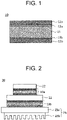
- Figure 1 is a longitudinal sectional view showing a schematic configuration of a layered bonding material 10 according to the embodiment.
- the layered bonding material 10 includes a base material 11 and pieces of lead-free solder 12a and 12b with which a first surface and a second surface of the base material 11 are coated.
- the base material 11 is made of a material having a coefficient of linear expansion of 5.5 to 15.5 ppm/K.
- the base material 11 more preferably has a coefficient of linear expansion of 5.9 to 14.4 ppm/K and particularly preferably has a coefficient of linear expansion of 7.0 to 11.6 ppm/K.
- a Cu-W-based material or a Cu-Mo-based material is used as the base material 11.
- a layered material of the Cu-W-based material and the Cu-Mo-based material may be used as the base material 11.
- any one of a composite material obtained by stacking a Cu-based material on both of a first surface and a second surface of the Cu-W-based material, a composite material obtained by stacking the Cu-based material on both of a first surface and a second surface of the Cu-Mo-based material, and a composite material obtained by stacking the Cu-based material on both of a first surface and a second surface of the layered material of the Cu-W-based material and the Cu-Mo-based material may be used.
- a ratio of thicknesses of the Cu-Mo-based material, the Cu-W-based material, or the layered material of the Cu-W-based material and the Cu-Mo-based material located in the center and the Cu-based material stacked on one surface thereof may be, for example, 4:1 to 1:2.
- the Cu-W-based material means a material having the largest contents of Cu and W in a mass ratio among elements constituting the material. A total of the contents of Cu and W is preferably 50% or higher in a mass ratio with respect to the entire material.
- the Cu-W-based material may include elements other than Cu and W as impurities.
- the Cu-Mo-based material means a material having the largest contents of Cu and Mo in a mass ratio among elements constituting the material. A total of the contents of Cu and Mo is preferably 50% or higher in a mass ratio with respect to the entire material.
- the Cu-Mo-based material may include elements other than Cu and Mo as impurities.
- the Cu content of the base material 11 is preferably 60% or lower in a mass ratio.
- the Cu content of the base material 11 is preferably 15% or higher in a mass ratio.
- a first surface (in an illustrated example, the upper surface) and a second surface (in the illustrated example, the lower surface) of the base material 11 are coated with the pieces of lead-free solder 12a and 12b, respectively.
- the material of the pieces of lead-free solder 12a and 12b is not particularly limited.
- an SnAgCu-based alloy or the like may be used.
- the SnAgCu-based alloy means an alloy having the largest contents of Sn, Ag, and Cu in a mass ratio among elements constituting the alloy. A total of contents of Sn, Ag, and Cu is preferably 50% or higher in a mass ratio with respect to the entire alloy.
- the SnAgCu-based alloy may include elements other than Sn, Ag, and Cu as impurities.
- SAC305 Sn3.0Ag0.5Cu
- SAC305 Sn3.0Ag0.5Cu
- the lead-free solder 12a with which the first surface is coated and the lead-free solder 12b with which the second surface is coated may have the same composition or may have compositions different from each other.
- a melting point of the pieces of lead-free solder 12a and 12b is preferably 210°C or higher and may be 230°C or higher, may be 240°C or higher, or may be 250°C or higher.
- At least one of the thickness of the lead-free solder 12a with which the first surface is coated and the thickness of the lead-free solder 12b with which the second surface is coated is preferably 20 to 100 ⁇ m. Both of the thickness of the lead-free solder 12a with which the first surface is coated and the thickness of the lead-free solder 12b with which the second surface is coated may be 20 to 100 ⁇ m.
- At least one of a ratio of the thicknesses of the base material 11 and the lead-free solder 12a with which the first surface is coated and a ratio of the thicknesses of the base material 11 and the lead-free solder 12b with which the second surface is coated is preferably 2:1 to 10:1. Both of the ratio of the thicknesses of the base material 11 and the lead-free solder 12a with which the first surface is coated and the ratio of the thicknesses of the base material 11 and the lead-free solder 12b with which the second surface is coated may be 2:1 to 10:1.
- the coating of the pieces of lead-free solder 12a and 12b is performed by an existing method such as plating.
- the thicknesses of the coating may be adjusted by cladding.
- an interface between at least one of the first surface and the second surface of the base material 11 and the lead-free solder 12a or 12b is preferably undercoated (for example, plating) with Ni and Sn in order from the base material 11 side. Since an interface between the base material 11 and Sn is undercoated with Ni, diffusion of Sn to the base material 11 side can be suppressed. Since Sn is undercoated on Ni, it is easy to perform the coating of the pieces of lead-free solder 12a and 12b. Therefore, adhesion of the base material 11 and the pieces of lead-free solder 12a and 12b is improved. Interfaces between both of the first surface and the second surface of the base material 11 and the pieces of lead-free solder 12a and 12b may be undercoated (for example, plating) with Ni and Sn in order from the base material 11 side.
- a first undercoat layer 13a by the undercoat treatment is formed between the first surface of the base material 11 and the lead-free solder 12a.
- a second undercoat layer 13b by the undercoat treatment is formed between the second surface of the base material 11 and the lead-free solder 12b.
- a semiconductor package 20 according to the embodiment is explained with reference to Figure 2 .
- a semiconductor device 22 included in the semiconductor package 20 is a power semiconductor device
- such a semiconductor package 20 is sometimes referred to as power module.
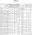
- Figure 2 is a longitudinal sectional view showing a schematic configuration of the semiconductor package 20 according to the embodiment.
- the semiconductor package 20 includes a substrate 21, a semiconductor device 22 disposed on the substrate 21, and a first layered bonding material 10a that bonds the substrate 21 and the semiconductor device 22.
- the configuration of the first layered bonding material 10a is the same as the configuration of the layered bonding material 10 according to the embodiment explained above. Explanation of the configuration of the first layered bonding material 10a is omitted.
- a type of the substrate 21 is not particularly limited.
- a DBC (Direct Bonded Copper) substrate or a DBA (Direct Bonded Aluminum) substrate is used.
- the semiconductor device 22 is disposed on the substrate 21 via the first layered bonding material 10a.
- the substrate 21 and the semiconductor device 22 are bonded by the first layered bonding material 10a.
- a type of the semiconductor device 22 is not particularly limited.
- a power semiconductor device such as a power transistor or a power diode is used.
- the temperature of the first layered bonding material 10a reaches high temperature equal to or higher than 200°C because of a rise in an operating temperature of the semiconductor device 22, if a melting point of the pieces of lead-free solder 12a and 12b is 210°C or higher in the first layered bonding material 10a, the pieces of lead-free solder 12a and 12b can be prevented from melting to cause a breakdown.
- the semiconductor package 20 further includes a heat radiating section 23 disposed on the substrate 21 and a second layered bonding material 10b that bonds the substrate 21 and the heat radiating section 23.
- the configuration of the second layered bonding material 10b is the same as the configuration of the layered bonding material 10 according to the embodiment explained above. Explanation of the configuration of the second layered bonding material 10b is omitted.
- the heat radiating section 23 is disposed on the opposite side of the semiconductor device 22 on the substrate 21 via the second layered bonding material 10b.
- the substrate 21 and the heat radiating section 23 are bonded by the second layered bonding material 10b.
- the heat radiating section 23 includes a heat radiating plate 23a and a heat radiating fin 23b closely attached and fixed to one surface (in the illustrated example, the lower surface) of the heat radiating plate 23a.
- the other surface (in the illustrated example, the upper surface) of the heat radiating plate 23a is closely attached and fixed to the second layered bonding material 10b.
- a material having high thermal conductivity is used. For example, CuMo or CuW is used.
- a coefficient of linear expansion of the base material 11 included in the first layered bonding material 10a and the second layered bonding material 10b is present in the middle between a coefficient of linear expansion of the semiconductor device 22 and a coefficient of linear expansion of the material of the substrate 21 and the heat radiating section 23 and is balanced.
- the base material 11 included in the first layered bonding material 10a and the second layered bonding material 10b is made of any one of a Cu-W-based material, a Cu-Mo-based material, a layered material of the Cu-W-based material and the Cu-Mo-based material, a composite material obtained by stacking a Cu-based material on both of a first surface and a second surface of the Cu-W-based material, a composite material obtained by stacking the Cu-based material on both of a first surface and a second surface of the Cu-Mo-based material, and a composite material obtained by stacking the Cu-based material on both of a first surface and a second surface of the layered material of the Cu-W-based material and the Cu-Mo-based material.
- the base material 11 has high thermal conductivity, it is possible to prevent an excessive temperature rise in the bonding section, a thermal distortion itself that occurs in the bonding section is reduced, and, as a result, this more advantageously acts on the extension of the life of a product of the semiconductor package 20.
- a Cu content of the base material 11 included in the first layered bonding material 10a and the second layered bonding material 10b is 60% or lower. Therefore, the coefficient of linear expansion of the base material 11 is lower. It is possible to further relax a distortion that occurs in the bonding section due to the CTE difference, in particular, under a high-temperature environment.
- a Cu content of the base material 11 included in the first layered bonding material 10a and the second layered bonding material 10b is 15% or higher. Therefore, the thermal conductivity of the base material 11 is improved and a thermal distortion itself that occurs in the bonding section can be further reduced.
- the interface between at least one of the first surface and the second surface of the base material 11 and the lead-free solder 12a or 12b is undercoated with Ni and Sn in order from the base material 11 side. Therefore, it is possible to improve adhesion of the base material 11 and the pieces of lead-free solder 12a and 12b.
- the melting point of the pieces of lead-free solder 12a and 12b is 210°C or higher. Therefore, even when the temperature of the first layered bonding material 10a and the second layered bonding material 10b reaches high temperature equal to or higher than 200°C because of a rise in an operating temperature of the semiconductor device 22, the pieces of lead-free solder 12a and 12b included in the first layered bonding material 10a and the second layered bonding material 10b can be prevented from melting to cause a breakdown.
- the present inventors prepared bonding materials (6.5 mm square) of examples 1 to 20 and comparative examples 1 to 7 and created samples obtained by bonding a substrate (20 mm square; a Cu block having a thickness of 2 mm) and a semiconductor device (5.5 mm square; an Si chip having a thickness of 0.4 mm) using the bonding materials. Subsequently, the present inventors carried out a cooling and heating cycle test for the samples using a cold impact device TSA-71L-A (manufactured by Espec Corporation) under a test condition of -40°C to +150°C (exposure times of 0.5 h).
- TSA-71L-A manufactured by Espec Corporation
- the present inventors performed SAT observation for the samples at points in time before the cooling and heating cycle test, after 250 cycles, after 500 cycles, and after 1000 cycles from each of an Si chip side and a Cu base side using an ultrasonic video device FineSAT FAS200II (manufactured by Hitachi Kenki Fine Tech Co., Ltd.), calculated a defect part area ratio of a bonding section from an SAT observation image, and evaluated a change ratio of the defect part area ratio (a defect part change ratio).
- the defect part change ratio was calculated by the following Expression (1) .
- Defect part change ratio (%) ⁇ (defect part area ratio after 1000 cycles - defect part area ratio before the cooling and heating cycle test) / defect part area ratio after 1000 cycles ⁇ ⁇ 100 Expression (1)
- a row of the "defect part change ratio" in Figure 3 and Figure 4 indicates a test result.
- the defect part change ratio of " ⁇ " indicates that the defect part change ratio on the Si chip side is lower than 50% and the defect part change ratio on the Cu base side is lower than 99.5%.
- the defect part change ratio of " ⁇ ” indicates that the defect part change ratio on the Si chip side is lower than 50% but the defect part change ratio on the Cu base side is 99.5% or higher.
- the defect part change ratio of " ⁇ ” indicates that the defect part change ratio on the Si chip side is 50% or higher.
- Figure 5 is a bar graph showing the defect part change ratios of the examples 1 and 2 and the comparative examples 1 and 2 in comparison.
- Figure 6 is a bar graph showing the defect part change ratios of the examples 3 and 4 and the comparative example 3 in comparison.
- Figure 7 is a bar graph showing the defect part change ratios of the examples 5 and 6 and the comparative examples 4 to 5 in comparison.
- a coefficient of linear expansion of a base material is 5.9 to 14.4 ppm/K.
- the base material is absent, in the comparative examples 2, 3, and 5, the coefficient of linear expansion of the base material is as high as 17.1 ppm/K, and, in the comparative examples 6 and 7, the coefficient of linear expansion of the base material is as low as 4.6 to 5.2 ppm/K.
- the defect part change ratio on the Si chip side after 1000 cycles is lower than 50%. It can be considered that it is possible to relax, in particular, a distortion that occurs in the bonding section on the Si chip side and achieve high reliability.
- the defect part change ratio on the Cu base side was lower than 99.5% and a relaxing effect for a distortion that occurred in the bonding section on the Cu base side was higher.
- the coefficient of linear expansion of the base material is 7.0 to 11.6 ppm/K in the examples 1 to 6, 9 to 10, and 12 to 18, the coefficient of linear expansion of the base material is 5.9 to 6.8 ppm/K in the examples 7 to 8 and 11 and the coefficient of linear expansion of the base material is 13.8 to 14.4 ppm/K in the examples 19 and 20.
- the coefficient of linear expansion of the base material is considered to be more preferably 7.0 to 11.6 ppm/K.
Landscapes
- Engineering & Computer Science (AREA)
- Mechanical Engineering (AREA)
- Chemical & Material Sciences (AREA)
- Materials Engineering (AREA)
- Metallurgy (AREA)
- Organic Chemistry (AREA)
- Cooling Or The Like Of Semiconductors Or Solid State Devices (AREA)
- Die Bonding (AREA)
- Structures Or Materials For Encapsulating Or Coating Semiconductor Devices Or Solid State Devices (AREA)
Abstract
Description
- The present disclosure relates to a layered bonding material, a semiconductor package, and a power module.
- Recently, required characteristics of semiconductor devices have become higher. SiC, GaAs, GaN, and the like are used in addition to Si, which has been used as a material of semiconductor devices. Semiconductor devices made of these materials have excellent characteristics including a rise in an operating temperature and expanded bandgaps. The semiconductor devices are applied to power semiconductor devices such as a power transistor.
- The power semiconductor devices are capable of performing a high-temperature operation. The temperature of a solder joint in a bonding section sometimes reaches high temperature equal to or higher than 200°C. Under such a high-temperature environment, there is a problem in that a distortion due to a difference between CTEs (Coefficients of Thermal Expansion) of a semiconductor device and a substrate occurs in a bonding section between the semiconductor device and the substrate, a crack occurs from the distortion, and, as a result, the life of the power semiconductor product is reduced.
-
Japanese Patent Laid-Open No. 2009-269075 -
Japanese Patent Laid-Open No. 2015-23183 -
Japanese Patent Laid-Open No. 2009-147111 - It is desired to provide a layered bonding material, a semiconductor package, and a power module that can relax a distortion that occurs in a bonding section, in particular, under a high-temperature environment.
- In a layered bonding material according to an embodiment, a coefficient of linear expansion of a base material is 5.5 to 15.5 ppm/K and a first surface and a second surface of the base material are coated with lead-free solder.
-
- [
Figure 1] Figure 1 is a longitudinal sectional view showing a schematic configuration of a layered bonding material according to an embodiment. - [
Figure 2] Figure 2 is a longitudinal sectional view showing a schematic configuration of a semiconductor package according to the embodiment. - [
Figure 3] Figure 3 is a table showing the configuration of a bonding member used in a cooling and heating cycle test. - [
Figure 4] Figure 4 is a table showing the configuration of the bonding member used in the cooling and heating cycle test. - [
Figure 5] Figure 5 is a bar graph showing defect part change ratios of examples 1 and 2 and comparative examples 1 and 2 in comparison. - [
Figure 6] Figure 6 is a bar graph showing defect part change ratios of examples 3 and 4 and a comparative example 3 in comparison. - [
Figure 7] Figure 7 is a bar graph showing defect part change ratios of examples 5 and 6 and comparative examples 4 and 5 in comparison. - As a result of, while conforming to environmental regulations such as the RoHS, repeating intensive studies in order to find a technique that can relax a distortion that occurs in a bonding section, the present inventors came to know that a distortion that occurs in the bonding section due to a CTE difference between a semiconductor device and a substrate can be relaxed by using a material having a coefficient of thermal expansion within a predetermined range as a core material while adopting lead-free solder as solder of the bonding section. Further, the present inventors came to know that an excessive temperature rise of the bonding section can be suppressed and, as a result, the life of a product can be greatly extended compared with the related art by using, in particular, a Cu-W-based material or a Cu-Mo-based material (or a layered material or a composite material thereof) as the core material while adopting the lead-free solder as the solder of the bonding section. An embodiment explained below has been devised based on such knowledge.
- In a layered bonding material according to a first aspect of the embodiment, a coefficient of linear expansion of a base material is 5.5 to 15.5 ppm/K, and a first surface and a second surface of the base material are coated with lead-free solder.
- When the present inventors actually performed verification with a cooling and heating cycle test, it was found that, according to such an aspect, it is possible to relax a distortion that occurs in a bonding section, in particular, under a high-temperature environment and achieve high reliability. According to the idea of the present inventors, the coefficient of linear expansion of the base material is present in the middle between a coefficient of linear expansion of a semiconductor device and a coefficient of linear expansion of a material of a substrate and a heat radiating section and is balanced. Therefore, it is considered possible to relax a distortion that occurs in the bonding section due to a CTE difference between the semiconductor device and the substrate, in particular, under a high-temperature environment.
- A layered bonding material according to a second aspect of the embodiment is the layered bonding material according to the first aspect, wherein the coefficient of linear expansion of the base material is 5.9 to 14.4 ppm/K.
- When the present inventors actually performed verification with the cooling and heating cycle test, it was found that, according to such an aspect, it is possible to relax a distortion that occurs in a bonding section on the semiconductor device side, in particular, under a high-temperature environment and achieve high reliability.
- A layered bonding material according to a third aspect of the embodiment is the layered bonding material according to the first or second aspect, wherein the coefficient of linear expansion of the base material is 7.0 to 11.6 ppm/K.
- When the present inventors actually performed verification with the cooling and heating cycle test, it was found that, according to such an aspect, an effect of relaxing a distortion that occurs in a bonding section on the substrate side is higher and it is possible to achieve higher reliability.
- A layered bonding material according to a fourth aspect of the embodiment is the layered bonding material according to any one of the first to third aspects, wherein the base material is made of any one of a Cu-W-based material, a Cu-Mo-based material, a layered material of the Cu-W-based material and the Cu-Mo-based material, a composite material obtained by stacking a Cu-based material on both of a first surface and a second surface of the Cu-W-based material, a composite material obtained by stacking the Cu-based material on both of a first surface and a second surface of the Cu-Mo-based material, and a composite material obtained by stacking the Cu-based material on both of a first surface and a second surface of the layered material of the Cu-W-based material and the Cu-Mo-based material.
- According to such an aspect, since the base material has high thermal conductivity, it is possible to prevent an excessive temperature rise in the bonding section, a thermal distortion itself that occurs in the bonding section is reduced, and, as a result, this more advantageously acts on the extension of the life of a product.
- A layered bonding material according to a fifth aspect of the embodiment is the layered bonding material according to any one of the first to fourth aspects, wherein a Cu content of the base material is 60% or lower.
- According to such an aspect, since the coefficient of linear expansion of the base material is lower, it is possible to further relax a distortion that occurs in the bonding section due to the CTE difference, in particular, under a high-temperature environment.
- A layered bonding material according to a sixth aspect of the embodiment is the layered bonding material according to any one of the first to fifth aspects, wherein a Cu content of the base material is 15% or higher.
- According to such an aspect, since the thermal conductivity of the base material is further improved, a thermal distortion itself that occurs in the bonding section can be further reduced.
- A layered bonding material according to a seventh aspect of the embodiment is the layered bonding material according to any one of the first to sixth aspects, wherein an interface between at least one of the first surface and the second surface of the base material and the lead-free solder is undercoated with Ni and Sn in order from the base material side.
- According to such an aspect, it is possible to improve adhesion of the base material and the lead-free solder.
- A layered bonding material according to an eighth aspect of the embodiment is the layered bonding material according to any one of the first to seventh aspects, wherein at least one of a thickness of the lead-free solder with which the first surface is coated and a thickness of the lead-free solder with which the second surface is coated is 20 to 100 µm.
- A layered bonding material according to a ninth aspect of the embodiment is the layered bonding material according to any one of the first to eighth aspects, wherein at least one of a ratio of thicknesses of the base material and the lead-free solder with which the first surface is coated and a ratio of thicknesses of the base material and the lead-free solder with which the second surface is coated is 2:1 to 10:1.
- A layered bonding material according to a tenth aspect of the embodiment is the layered bonding material according to any one of the first to ninth aspects, wherein a melting point of the lead-free solder is 210°C or higher. The melting point of the lead-free solder may be 230°C or higher.
- According to such an aspect, even when the temperature of the layered bonding material reaches high temperature equal to or higher than 200°C because of a rise in an operating temperature of the semiconductor device, the lead-free solder included in the layered bonding material can be prevented from melting to cause a breakdown.
- A semiconductor package according to an eleventh aspect of the embodiment includes: a substrate; a semiconductor device disposed on the substrate; and a layered bonding material disposed between the substrate and the semiconductor device and bonding the substrate and the semiconductor device, wherein, in the layered bonding material, a coefficient of linear expansion of a base material is 5.5 to 15.5 ppm/K, and a first surface and a second surface of the base material are coated with lead-free solder.
- When the present inventors actually performed verification with a cooling and heating cycle test, it was found that, according to such an aspect, it is possible to relax a distortion that occurs in a bonding section, in particular, under a high-temperature environment and achieve high reliability. According to the idea of the present inventors, the coefficient of linear expansion of the base material included in the layered bonding material is present in the middle between a coefficient of linear expansion of a material of the semiconductor device and a coefficient of linear expansion of the substrate and is balanced. Therefore, it is considered possible to relax a distortion that occurs in the bonding section due to a CTE difference between the semiconductor device and the substrate, in particular, under a high-temperature environment.
- A semiconductor package according to a twelfth aspect of the embodiment includes: a substrate; a semiconductor device disposed on the substrate; a first layered bonding material disposed between the substrate and the semiconductor device and bonding the substrate and the semiconductor device; a heat radiating section disposed on an opposite side of the semiconductor device on the substrate; and a second layered bonding material disposed between the substrate and the heat radiating section and bonding the substrate and the heat radiating section, wherein, in at least one of the first layered bonding material and the second layered bonding material, a coefficient of linear expansion of a base material is 5.5 to 15.5 ppm/K, and a first surface and a second surface of the base material are coated with lead-free solder.
- When the present inventors actually performed verification with a cooling and heating cycle test, it was found that, according to such an aspect, it is possible to relax a distortion that occurs in a bonding section, in particular, under a high-temperature environment and achieve high reliability. According to the idea of the present inventors, the coefficient of linear expansion of the base material included in the layered bonding material is present in the middle between a coefficient of linear expansion of the semiconductor device and a coefficient of linear expansion of a material of the substrate and the heat radiating section and is balanced. Therefore, it is considered possible to relax a distortion that occurs in the bonding section due to a CTE difference between the semiconductor device and the substrate, in particular, under a high-temperature environment.
- A semiconductor package according to a thirteenth aspect of the embodiment is the semiconductor package according to the eleventh or twelfth aspect, wherein the coefficient of linear expansion of the base material is 5.9 to 14.4 ppm/K.
- When the present inventors actually performed verification with a cooling and heating cycle test, it was found that, according to such an aspect, it is possible to relax a distortion that occurs in the bonding section on the semiconductor device side, in particular, under a high-temperature environment and achieve high reliability.
- A semiconductor package according to a fourteenth aspect of the embodiment is the semiconductor package according to any one of the eleventh to thirteenth aspects, wherein the coefficient of linear expansion of the base material is 7.0 to 11.6 ppm/K.
- When the present inventors actually performed verification with the cooling and heating cycle test, it was found that, according to such an aspect, an effect of relaxing a distortion that occurs in a bonding section on the substrate side is higher and it is possible to achieve higher reliability.
- A semiconductor package according to a fifteenth aspect of the embodiment is the semiconductor package according to any one of the eleventh to fourteenth aspects, wherein the base material is made of any one of a Cu-W-based material, a Cu-Mo-based material, a layered material of the Cu-W-based material and the Cu-Mo-based material, a composite material obtained by stacking a Cu-based material on both of a first surface and a second surface of the Cu-W-based material, a composite material obtained by stacking the Cu-based material on both of a first surface and a second surface of the Cu-Mo-based material, and a composite material obtained by stacking the Cu-based material on both of a first surface and a second surface of the layered material of the Cu-W-based material and the Cu-Mo-based material.
- According to such an aspect, since the base material has high thermal conductivity, it is possible to prevent an excessive temperature rise in the bonding section, a thermal distortion itself that occurs in the bonding section is reduced, and, as a result, this more advantageously acts on the extension of the life of a product.
- A semiconductor package according to a sixteenth aspect of the embodiment is the semiconductor package according to any one of the eleventh to fifteenth aspects, wherein a Cu content of the base material is 60% or lower.
- According to such an aspect, since the coefficient of linear expansion of the base material included in the layered bonding material is lower, it is possible to further relax a distortion that occurs in the bonding section due to the CTE difference, in particular, under a high-temperature environment.
- A semiconductor package according to a seventeenth aspect of the embodiment is the semiconductor package according to any one of the eleventh to sixteenth aspects, wherein a Cu content of the base material is 15% or higher.
- According to such an aspect, since the thermal conductivity of the base material included in the layered bonding material is further improved, a thermal distortion itself that occurs in the bonding section can be further reduced.
- A semiconductor package according to an eighteenth aspect of the embodiment is the semiconductor package according to any one of the eleventh to seventeenth aspects, wherein an interface between at least one of the first surface and the second surface of the base material and the lead-free solder is undercoated with Ni and Sn in order from the base material side.
- According to such an aspect, it is possible to improve adhesion of the base material included in the layered bonding material and the lead-free solder.
- A semiconductor package according to a nineteenth aspect of the embodiment is the semiconductor package according to any one of the eleventh to eighteenth aspects, wherein at least one of a thickness of the lead-free solder with which the first surface is coated and a thickness of the lead-free solder with which the second surface is coated is 20 to 100 µm.
- A semiconductor package according to a twentieth aspect of the embodiment is the semiconductor package according to any one of the eleventh to nineteenth aspects, wherein at least one of a ratio of thicknesses of the base material and the lead-free solder with which the first surface is coated and a ratio of thicknesses of the base material and the lead-free solder with which the second surface is coated is 2:1 to 10:1.
- A semiconductor package according to a twenty-first aspect of the embodiment is the semiconductor package according to any one of the eleventh to twentieth aspects, wherein a melting point of the lead-free solder is 210°C or higher. The melting point of the lead-free solder may be 230°C or higher.
- According to such an aspect, even when the temperature of the layered bonding material reaches high temperature equal to or higher than 200°C because of a rise in an operating temperature of the semiconductor device, the lead-free solder included in the layered bonding material can be prevented from melting to cause a breakdown.
- A power module according to a twenty-second aspect of the embodiment includes: a substrate; a power semiconductor device disposed on the substrate; and a layered bonding material disposed between the substrate and the power semiconductor device and bonding the substrate and the power semiconductor device, wherein, in the layered bonding material, a coefficient of linear expansion of a base material is 5.5 to 15.5 ppm/K or less, and a first surface and a second surface of the base material are coated with lead-free solder.
- When the present inventors actually performed verification with a cooling and heating cycle test, it was found that, according to such an aspect, it is possible to relax a distortion that occurs in a bonding section, in particular, under a high-temperature environment and achieve high reliability. According to the idea of the present inventors, the coefficient of linear expansion of the base material included in the layered bonding material is present in the middle between a coefficient of linear expansion of the semiconductor device and a coefficient of linear expansion of the substrate and is balanced. Therefore, it is considered possible to relax a distortion that occurs in the bonding section due to a CTE difference between the semiconductor device and the substrate, in particular, under a high-temperature environment.
- A power module according to a twenty-third aspect of the embodiment includes: a substrate; a power semiconductor device disposed on the substrate; a first layered bonding material disposed between the substrate and the power semiconductor device and bonding the substrate and the power semiconductor device; a heat radiating section disposed on an opposite side of the power semiconductor device on the substrate; and a second layered bonding material disposed between the substrate and the heat radiating section and bonding the substrate and the heat radiating section, wherein, in at least one of the first layered bonding material and the second layered bonding material, a coefficient of linear expansion of a base material is 5.5 to 15.5 ppm/K or less, and a first surface and a second surface of the base material are coated with lead-free solder.
- When the present inventors actually performed verification with a cooling and heating cycle test, it was found that, according to such an aspect, it is possible to relax a distortion that occurs in a bonding section, in particular, under a high-temperature environment and achieve high reliability. According to the idea of the present inventors, the coefficient of linear expansion of the base material included in the layered bonding material is present in the middle between a coefficient of linear expansion of the semiconductor device and a coefficient of linear expansion of a material of the substrate and the heat radiating section and is balanced. Therefore, it is considered possible to relax a distortion that occurs in the bonding section due to a CTE difference between the semiconductor device and the substrate, in particular, under a high-temperature environment.
- A power module according to a twenty-fourth aspect of the embodiment is the power module according to the twenty-second or twenty-third aspect, wherein the coefficient of linear expansion of the base material is 5.9 to 14.4 ppm/K.
- When the present inventors actually performed verification with a cooling and heating cycle test, it was found that, according to such an aspect, it is possible to relax a distortion that occurs in a bonding section on the semiconductor device side, in particular, under a high-temperature environment and achieve high reliability.
- A power module according to a twenty-fifth aspect of the embodiment is the power module according to any one of the twenty-second to twenty-fourth aspects, wherein the coefficient of linear expansion of the base material is 7.0 to 11.6 ppm/K.
- When the present inventors actually performed verification with the cooling and heating cycle test, it was found that, according to such an aspect, an effect of relaxing a distortion that occurs in a bonding section on the substrate side is higher and it is possible to achieve higher reliability.
- A power module according to a twenty-sixth aspect of the embodiment is the power module according to any one of the twenty-second to twenty-fifth aspects, wherein the base material is made of any one of a Cu-W-based material, a Cu-Mo-based material, a layered material of the Cu-W-based material and the Cu-Mo-based material, a composite material obtained by stacking a Cu-based material on both of a first surface and a second surface of the Cu-W-based material, a composite material obtained by stacking the Cu-based material on both of a first surface and a second surface of the Cu-Mo-based material, and a composite material obtained by stacking the Cu-based material on both of a first surface and a second surface of the layered material of the Cu-W-based material and the Cu-Mo-based material.
- According to such an aspect, since the base material has high thermal conductivity, it is possible to prevent an excessive temperature rise in the bonding section, a thermal distortion itself that occurs in the bonding section is reduced, and, as a result, this more advantageously acts on the extension of the life of a product.
- A power module according to a twenty-seventh aspect of the embodiment is the power module according to any one of the twenty-second to twenty-sixth aspects, wherein a Cu content of the base material is 60% or lower.
- According to such an aspect, since the coefficient of linear expansion of the base material included in the layered bonding material is lower, it is possible to further relax a distortion that occurs in the bonding section due to the CTE difference, in particular, under a high-temperature environment.
- A power module according to a twenty-eighth aspect of the embodiment is the power module according to any one of the twenty-second to twenty-seventh aspects, wherein a Cu content of the base material is 15% or higher.
- According to such an aspect, since the thermal conductivity of the base material included in the layered bonding material is further improved, a thermal distortion itself that occurs in the bonding section can be further reduced.
- A power module according to a twenty-ninth aspect of the embodiment is the power module according to any one of the twenty-second to twenty-eighth aspects, wherein an interface between at least one of the first surface and the second surface of the base material and the lead-free solder is undercoated with Ni and Sn in order from the base material side.
- According to such an aspect, it is possible to improve adhesion of the base material included in the layered bonding material and the lead-free solder.
- A power module according to a thirtieth aspect of the embodiment is the power module according to any one of the twenty-second to twenty-ninth aspects, wherein at least one of a thickness of the lead-free solder with which the first surface is coated and a thickness of the lead-free solder with which the second surface is coated is 20 to 100 µm.
- A power module according to a thirty-first aspect of the embodiment is the power module according to any one of the twenty-second to thirtieth aspects, wherein at least one of a ratio of thicknesses of the base material and the lead-free solder with which the first surface is coated and a ratio of thicknesses of the base material and the lead-free solder with which the second surface is coated is 2:1 to 10:1.
- A power module according to a thirty-second aspect of the embodiment is the power module according to any one of the twenty-second to thirty-first aspects, wherein a melting point of the lead-free solder is 210°C or higher. The melting point of the lead-free solder may be 230°C or higher.
- According to such an aspect, even when the temperature of the layered bonding material reaches high temperature equal to or higher than 200°C because of a rise in an operating temperature of the power semiconductor device, the lead-free solder included in the layered bonding material can be prevented from melting to cause a breakdown.
- A specific example of the embodiment is explained in detail below with reference to the accompanying drawings. Note that, in the following explanation and the drawings referred to in the following explanation, the same reference numerals and signs are used for portions that can be configured the same. Redundant explanation of the portions is omitted.
-
Figure 1 is a longitudinal sectional view showing a schematic configuration of a layeredbonding material 10 according to the embodiment. - As shown in
Figure 1 , the layeredbonding material 10 includes abase material 11 and pieces of lead-free solder 12a and 12b with which a first surface and a second surface of thebase material 11 are coated. - Of the layered
bonding material 10, thebase material 11 is made of a material having a coefficient of linear expansion of 5.5 to 15.5 ppm/K. Thebase material 11 more preferably has a coefficient of linear expansion of 5.9 to 14.4 ppm/K and particularly preferably has a coefficient of linear expansion of 7.0 to 11.6 ppm/K. Specifically, for example, a Cu-W-based material or a Cu-Mo-based material is used as thebase material 11. A layered material of the Cu-W-based material and the Cu-Mo-based material may be used as thebase material 11. As thebase material 11, any one of a composite material obtained by stacking a Cu-based material on both of a first surface and a second surface of the Cu-W-based material, a composite material obtained by stacking the Cu-based material on both of a first surface and a second surface of the Cu-Mo-based material, and a composite material obtained by stacking the Cu-based material on both of a first surface and a second surface of the layered material of the Cu-W-based material and the Cu-Mo-based material may be used. When thebase material 11 is made of the composite material, a ratio of thicknesses of the Cu-Mo-based material, the Cu-W-based material, or the layered material of the Cu-W-based material and the Cu-Mo-based material located in the center and the Cu-based material stacked on one surface thereof may be, for example, 4:1 to 1:2. - Note that, in this specification, the Cu-W-based material means a material having the largest contents of Cu and W in a mass ratio among elements constituting the material. A total of the contents of Cu and W is preferably 50% or higher in a mass ratio with respect to the entire material. The Cu-W-based material may include elements other than Cu and W as impurities. The Cu-Mo-based material means a material having the largest contents of Cu and Mo in a mass ratio among elements constituting the material. A total of the contents of Cu and Mo is preferably 50% or higher in a mass ratio with respect to the entire material. The Cu-Mo-based material may include elements other than Cu and Mo as impurities.
- Since a coefficient of thermal expansion increases when the Cu content of the
base material 11 increases, the Cu content of thebase material 11 is preferably 60% or lower in a mass ratio. - Since thermal conductivity is improved when the Cu content of the
base material 11 increases, the Cu content of thebase material 11 is preferably 15% or higher in a mass ratio. - As shown in
Figure 1 , a first surface (in an illustrated example, the upper surface) and a second surface (in the illustrated example, the lower surface) of thebase material 11 are coated with the pieces of lead-free solder 12a and 12b, respectively. - The material of the pieces of lead-
free solder 12a and 12b is not particularly limited. For example, an SnAgCu-based alloy or the like may be used. Note that the SnAgCu-based alloy means an alloy having the largest contents of Sn, Ag, and Cu in a mass ratio among elements constituting the alloy. A total of contents of Sn, Ag, and Cu is preferably 50% or higher in a mass ratio with respect to the entire alloy. The SnAgCu-based alloy may include elements other than Sn, Ag, and Cu as impurities. Specifically, for example, SAC305 (Sn3.0Ag0.5Cu) may be used as the pieces of lead-free solder 12a and 12b. - The lead-
free solder 12a with which the first surface is coated and the lead-free solder 12b with which the second surface is coated may have the same composition or may have compositions different from each other. - A melting point of the pieces of lead-
free solder 12a and 12b is preferably 210°C or higher and may be 230°C or higher, may be 240°C or higher, or may be 250°C or higher. - At least one of the thickness of the lead-
free solder 12a with which the first surface is coated and the thickness of the lead-free solder 12b with which the second surface is coated is preferably 20 to 100 µm. Both of the thickness of the lead-free solder 12a with which the first surface is coated and the thickness of the lead-free solder 12b with which the second surface is coated may be 20 to 100 µm. - At least one of a ratio of the thicknesses of the
base material 11 and the lead-free solder 12a with which the first surface is coated and a ratio of the thicknesses of thebase material 11 and the lead-free solder 12b with which the second surface is coated is preferably 2:1 to 10:1. Both of the ratio of the thicknesses of thebase material 11 and the lead-free solder 12a with which the first surface is coated and the ratio of the thicknesses of thebase material 11 and the lead-free solder 12b with which the second surface is coated may be 2:1 to 10:1. - The coating of the pieces of lead-
free solder 12a and 12b is performed by an existing method such as plating. The thicknesses of the coating may be adjusted by cladding. - As shown in
Figure 1 , an interface between at least one of the first surface and the second surface of thebase material 11 and the lead-free solder 12a or 12b is preferably undercoated (for example, plating) with Ni and Sn in order from thebase material 11 side. Since an interface between thebase material 11 and Sn is undercoated with Ni, diffusion of Sn to thebase material 11 side can be suppressed. Since Sn is undercoated on Ni, it is easy to perform the coating of the pieces of lead-free solder 12a and 12b. Therefore, adhesion of thebase material 11 and the pieces of lead-free solder 12a and 12b is improved. Interfaces between both of the first surface and the second surface of thebase material 11 and the pieces of lead-free solder 12a and 12b may be undercoated (for example, plating) with Ni and Sn in order from thebase material 11 side. - In the illustrated example, a
first undercoat layer 13a by the undercoat treatment is formed between the first surface of thebase material 11 and the lead-free solder 12a. Asecond undercoat layer 13b by the undercoat treatment is formed between the second surface of thebase material 11 and the lead-free solder 12b. - Subsequently, a
semiconductor package 20 according to the embodiment is explained with reference toFigure 2 . Note that, in this specification, when asemiconductor device 22 included in thesemiconductor package 20 is a power semiconductor device, such a semiconductor package 20 (that is, the power semiconductor package) is sometimes referred to as power module. -
Figure 2 is a longitudinal sectional view showing a schematic configuration of thesemiconductor package 20 according to the embodiment. - As shown in
Figure 2 , thesemiconductor package 20 includes asubstrate 21, asemiconductor device 22 disposed on thesubstrate 21, and a firstlayered bonding material 10a that bonds thesubstrate 21 and thesemiconductor device 22. - The configuration of the first
layered bonding material 10a is the same as the configuration of the layeredbonding material 10 according to the embodiment explained above. Explanation of the configuration of the firstlayered bonding material 10a is omitted. - A type of the
substrate 21 is not particularly limited. For example, a DBC (Direct Bonded Copper) substrate or a DBA (Direct Bonded Aluminum) substrate is used. - As shown in
Figure 2 , thesemiconductor device 22 is disposed on thesubstrate 21 via the firstlayered bonding material 10a. Thesubstrate 21 and thesemiconductor device 22 are bonded by the firstlayered bonding material 10a. - A type of the
semiconductor device 22 is not particularly limited. For example, a power semiconductor device such as a power transistor or a power diode is used. In this case, even if the temperature of the firstlayered bonding material 10a reaches high temperature equal to or higher than 200°C because of a rise in an operating temperature of thesemiconductor device 22, if a melting point of the pieces of lead-free solder 12a and 12b is 210°C or higher in the firstlayered bonding material 10a, the pieces of lead-free solder 12a and 12b can be prevented from melting to cause a breakdown. - In this embodiment, as shown in
Figure 2 , thesemiconductor package 20 further includes aheat radiating section 23 disposed on thesubstrate 21 and a secondlayered bonding material 10b that bonds thesubstrate 21 and theheat radiating section 23. - The configuration of the second
layered bonding material 10b is the same as the configuration of the layeredbonding material 10 according to the embodiment explained above. Explanation of the configuration of the secondlayered bonding material 10b is omitted. - As shown in
Figure 2 , theheat radiating section 23 is disposed on the opposite side of thesemiconductor device 22 on thesubstrate 21 via the secondlayered bonding material 10b. Thesubstrate 21 and theheat radiating section 23 are bonded by the secondlayered bonding material 10b. - In an example shown in
Figure 2 , theheat radiating section 23 includes aheat radiating plate 23a and a heat radiating fin 23b closely attached and fixed to one surface (in the illustrated example, the lower surface) of theheat radiating plate 23a. The other surface (in the illustrated example, the upper surface) of theheat radiating plate 23a is closely attached and fixed to the secondlayered bonding material 10b. As the material of theheat radiating section 23, a material having high thermal conductivity is used. For example, CuMo or CuW is used. - When the present inventors actually performed verification with a cooling and heating cycle test explained below, it was found that, according to this embodiment explained above, it is possible to relax a distortion that occurs in a bonding section, in particular, under a high-temperature environment and achieve high reliability. According to the idea of the present inventors, a coefficient of linear expansion of the
base material 11 included in the firstlayered bonding material 10a and the secondlayered bonding material 10b is present in the middle between a coefficient of linear expansion of thesemiconductor device 22 and a coefficient of linear expansion of the material of thesubstrate 21 and theheat radiating section 23 and is balanced. Therefore, it is considered possible to relax a distortion that occurs in a bonding section between thesemiconductor device 22 and thesubstrate 21 and a bonding section between thesubstrate 21 and theheat radiating section 23 because of a CTE difference between thesemiconductor device 22 and thesubstrate 21 and theheat radiating section 23, in particular, under a high-temperature environment. - According to this embodiment, the
base material 11 included in the firstlayered bonding material 10a and the secondlayered bonding material 10b is made of any one of a Cu-W-based material, a Cu-Mo-based material, a layered material of the Cu-W-based material and the Cu-Mo-based material, a composite material obtained by stacking a Cu-based material on both of a first surface and a second surface of the Cu-W-based material, a composite material obtained by stacking the Cu-based material on both of a first surface and a second surface of the Cu-Mo-based material, and a composite material obtained by stacking the Cu-based material on both of a first surface and a second surface of the layered material of the Cu-W-based material and the Cu-Mo-based material. Since thebase material 11 has high thermal conductivity, it is possible to prevent an excessive temperature rise in the bonding section, a thermal distortion itself that occurs in the bonding section is reduced, and, as a result, this more advantageously acts on the extension of the life of a product of thesemiconductor package 20. - According to this embodiment, a Cu content of the
base material 11 included in the firstlayered bonding material 10a and the secondlayered bonding material 10b is 60% or lower. Therefore, the coefficient of linear expansion of thebase material 11 is lower. It is possible to further relax a distortion that occurs in the bonding section due to the CTE difference, in particular, under a high-temperature environment. - According to this embodiment, a Cu content of the
base material 11 included in the firstlayered bonding material 10a and the secondlayered bonding material 10b is 15% or higher. Therefore, the thermal conductivity of thebase material 11 is improved and a thermal distortion itself that occurs in the bonding section can be further reduced. - According to this embodiment, in the first
layered bonding material 10a and the secondlayered bonding material 10b, the interface between at least one of the first surface and the second surface of thebase material 11 and the lead-free solder 12a or 12b is undercoated with Ni and Sn in order from thebase material 11 side. Therefore, it is possible to improve adhesion of thebase material 11 and the pieces of lead-free solder 12a and 12b. - According to this embodiment, in the first
layered bonding material 10a and the secondlayered bonding material 10b, the melting point of the pieces of lead-free solder 12a and 12b is 210°C or higher. Therefore, even when the temperature of the firstlayered bonding material 10a and the secondlayered bonding material 10b reaches high temperature equal to or higher than 200°C because of a rise in an operating temperature of thesemiconductor device 22, the pieces of lead-free solder 12a and 12b included in the firstlayered bonding material 10a and the secondlayered bonding material 10b can be prevented from melting to cause a breakdown. - Specific examples according to this embodiment are explained.
- As shown in
Figure 3 andFigure 4 , the present inventors prepared bonding materials (6.5 mm square) of examples 1 to 20 and comparative examples 1 to 7 and created samples obtained by bonding a substrate (20 mm square; a Cu block having a thickness of 2 mm) and a semiconductor device (5.5 mm square; an Si chip having a thickness of 0.4 mm) using the bonding materials. Subsequently, the present inventors carried out a cooling and heating cycle test for the samples using a cold impact device TSA-71L-A (manufactured by Espec Corporation) under a test condition of -40°C to +150°C (exposure times of 0.5 h). The present inventors performed SAT observation for the samples at points in time before the cooling and heating cycle test, after 250 cycles, after 500 cycles, and after 1000 cycles from each of an Si chip side and a Cu base side using an ultrasonic video device FineSAT FAS200II (manufactured by Hitachi Kenki Fine Tech Co., Ltd.), calculated a defect part area ratio of a bonding section from an SAT observation image, and evaluated a change ratio of the defect part area ratio (a defect part change ratio). The defect part change ratio was calculated by the following Expression (1) . - Defect part change ratio (%) = {(defect part area ratio after 1000 cycles - defect part area ratio before the cooling and heating cycle test) / defect part area ratio after 1000 cycles} × 100 Expression (1)
- A row of the "defect part change ratio" in
Figure 3 andFigure 4 indicates a test result. InFigure 3 andFigure 4 , the defect part change ratio of "⊙" indicates that the defect part change ratio on the Si chip side is lower than 50% and the defect part change ratio on the Cu base side is lower than 99.5%. The defect part change ratio of "∘" indicates that the defect part change ratio on the Si chip side is lower than 50% but the defect part change ratio on the Cu base side is 99.5% or higher. The defect part change ratio of "×" indicates that the defect part change ratio on the Si chip side is 50% or higher. -
Figure 5 is a bar graph showing the defect part change ratios of the examples 1 and 2 and the comparative examples 1 and 2 in comparison.Figure 6 is a bar graph showing the defect part change ratios of the examples 3 and 4 and the comparative example 3 in comparison.Figure 7 is a bar graph showing the defect part change ratios of the examples 5 and 6 and the comparative examples 4 to 5 in comparison. - As shown in
Figure 3 to Figure 7 , in all of the examples 1 to 20, it was confirmed that the defect part change ratio on the Si chip side after 1000 cycles was lower than 50%, a distortion that occurred in a bonding section on the Si chip side, in particular, under a high-temperature environment was successfully relaxed, and reliability was high. On the other hand, as shown inFigure 4 , in the comparative examples 1 to 7, it was confirmed that the defect part change ratio on the Si chip side after 1000 cycles was 50% or higher (in the comparative examples 1 to 5, 80% or higher), a distortion that occurred in the bonding section on the Si chip side, in particular, under a high-temperature environment was not successfully relaxed, and reliability was low. In the examples 1 to 20, a coefficient of linear expansion of a base material is 5.9 to 14.4 ppm/K. On the other hand, in the comparative examples 1 and 4, the base material is absent, in the comparative examples 2, 3, and 5, the coefficient of linear expansion of the base material is as high as 17.1 ppm/K, and, in the comparative examples 6 and 7, the coefficient of linear expansion of the base material is as low as 4.6 to 5.2 ppm/K. Therefore, in a layered bonding material in which a first surface and a second surface of a base material are coated with lead-free solder, if a coefficient of linear expansion of the base material is 5.5 (the middle of 5.9 and 4.6) to 15.5 (the middle of 14.4 and 17.1) ppm/K, more preferably, 5.9 to 14.4 ppm/K, the defect part change ratio on the Si chip side after 1000 cycles is lower than 50%. It can be considered that it is possible to relax, in particular, a distortion that occurs in the bonding section on the Si chip side and achieve high reliability. - As shown in
Figure 3 andFigure 4 , in the examples 1 to 6, 9 to 10, and 12 to 18, it was confirmed that the defect part change ratio on the Cu base side was lower than 99.5% and a relaxing effect for a distortion that occurred in the bonding section on the Cu base side was higher. Whereas the coefficient of linear expansion of the base material is 7.0 to 11.6 ppm/K in the examples 1 to 6, 9 to 10, and 12 to 18, the coefficient of linear expansion of the base material is 5.9 to 6.8 ppm/K in the examples 7 to 8 and 11 and the coefficient of linear expansion of the base material is 13.8 to 14.4 ppm/K in the examples 19 and 20. Accordingly, in the layered bonding material in which the first surface and the second surface of the base material are coated with the lead-free solder, in order to have a higher relaxing effect for a distortion that occurs in the bonding section and achieve higher reliability, the coefficient of linear expansion of the base material is considered to be more preferably 7.0 to 11.6 ppm/K. - The embodiment and the modifications are explained above by illustration. However, the scope of the present technique is not limited to the embodiment and the modifications and can be changed and modified according to a purpose within the scope described in claims. The embodiment and the modifications can be combined as appropriate in a range in which processing contents do not contradict.
Claims (35)
- A layered bonding material, wherein a coefficient of linear expansion of a base material is 5.5 to 15.5 ppm/K, and a first surface and a second surface of the base material are coated with lead-free solder.
- The layered bonding material according to claim 1,
wherein the coefficient of linear expansion of the base material is 5.9 to 14.4 ppm/K. - The layered bonding material according to claim 1 or 2, wherein the coefficient of linear expansion of the base material is 7.0 to 11.6 ppm/K.
- The layered bonding material according to claim 1, wherein the base material is made of any one of a Cu-W-based material, a Cu-Mo-based material, a layered material of the Cu-W-based material and the Cu-Mo-based material, a composite material obtained by stacking a Cu-based material on both of a first surface and a second surface of the Cu-W-based material, a composite material obtained by stacking the Cu-based material on both of a first surface and a second surface of the Cu-Mo-based material, and a composite material obtained by stacking the Cu-based material on both of a first surface and a second surface of the layered material of the Cu-W-based material and the Cu-Mo-based material.
- The layered bonding material according to any one of claims 1 to 4, wherein a Cu content of the base material is 60% or lower.
- The layered bonding material according to any one of claims 1 to 5, wherein a Cu content of the base material is 15% or higher.
- The layered bonding material according to any one of claims 1 to 6, wherein an interface between at least one of the first surface and the second surface of the base material and the lead-free solder is undercoated with Ni and Sn in order from the base material side.
- The layered bonding material according to any one of claims 1 to 7, wherein at least one of a thickness of the lead-free solder with which the first surface is coated and a thickness of the lead-free solder with which the second surface is coated is 20 to 100 µm.
- The layered bonding material according to any one of claims 1 to 8, wherein at least one of a ratio of thicknesses of the base material and the lead-free solder with which the first surface is coated and a ratio of thicknesses of the base material and the lead-free solder with which the second surface is coated is 2:1 to 10:1.
- The layered bonding material according to any one of claims 1 to 9, wherein a melting point of the lead-free solder is 210°C or higher.
- The layered bonding material according to claim 10, wherein the melting point of the lead-free solder is 230°C or higher.
- A semiconductor package comprising:a substrate;a semiconductor device disposed on the substrate; anda layered bonding material disposed between the substrate and the semiconductor device and bonding the substrate and the semiconductor device, whereinin the layered bonding material, a coefficient of linear expansion of a base material is 5.5 to 15.5 ppm/K, and a first surface and a second surface of the base material are coated with lead-free solder.
- A semiconductor package comprising:a substrate;a semiconductor device disposed on the substrate;a first layered bonding material disposed between the substrate and the semiconductor device and bonding the substrate and the semiconductor device;a heat radiating section disposed on an opposite side of the semiconductor device on the substrate; anda second layered bonding material disposed between the substrate and the heat radiating section and bonding the substrate and the heat radiating section, whereinin at least one of the first layered bonding material and the second layered bonding material, a coefficient of linear expansion of a base material is 5.5 to 15.5 ppm/K, and a first surface and a second surface of the base material are coated with lead-free solder.
- The semiconductor package according to claim 12 or 13, wherein the coefficient of linear expansion of the base material is 5.9 to 14.4 ppm/K.
- The semiconductor package according to any one of claims 12 to 14, wherein the coefficient of linear expansion of the base material is 7.0 to 11.6 ppm/K.
- The semiconductor package according to any one of claims 12 to 15, wherein the base material is made of any one of a Cu-W-based material, a Cu-Mo-based material, a layered material of the Cu-W-based material and the Cu-Mo-based material, a composite material obtained by stacking a Cu-based material on both of a first surface and a second surface of the Cu-W-based material, a composite material obtained by stacking the Cu-based material on both of a first surface and a second surface of the Cu-Mo-based material, and a composite material obtained by stacking the Cu-based material on both of a first surface and a second surface of the layered material of the Cu-W-based material and the Cu-Mo-based material.
- The semiconductor package according to any one of claims 12 to 16, wherein a Cu content of the base material is 60% or lower.
- The semiconductor package according to any one of claims 12 to 17, wherein a Cu content of the base material is 15% or higher.
- The semiconductor package according to any one of claims 12 to 18, wherein an interface between at least one of the first surface and the second surface of the base material and the lead-free solder is undercoated with Ni and Sn in order from the base material side.
- The semiconductor package according to any one of claims 12 to 19, wherein at least one of a thickness of the lead-free solder with which the first surface is coated and a thickness of the lead-free solder with which the second surface is coated is 20 to 100 µm.
- The semiconductor package according to any one of claims 12 to 20, wherein at least one of a ratio of thicknesses of the base material and the lead-free solder with which the first surface is coated and a ratio of thicknesses of the base material and the lead-free solder with which the second surface is coated is 2:1 to 10:1.
- The semiconductor package according to any one of claims 12 to 21, wherein a melting point of the lead-free solder is 210°C or higher.
- The semiconductor package according to claim 22, wherein the melting point of the lead-free solder is 230°C or higher.
- A power module comprising:a substrate;a power semiconductor device disposed on the substrate; anda layered bonding material disposed between the substrate and the power semiconductor device and bonding the substrate and the power semiconductor device, whereinin the layered bonding material, a coefficient of linear expansion of a base material is 5.5 to 15.5 ppm/K, and a first surface and a second surface of the base material are coated with lead-free solder.
- A power module comprising:a substrate;a power semiconductor device disposed on the substrate;a first layered bonding material disposed between the substrate and the power semiconductor device and bonding the substrate and the power semiconductor device;a heat radiating section disposed on an opposite side of the power semiconductor device on the substrate; anda second layered bonding material disposed between the substrate and the heat radiating section and bonding the substrate and the heat radiating section, whereinin at least one of the first layered bonding material and the second layered bonding material, a coefficient of linear expansion of a base material is 5.5 to 15.5 ppm/K, and a first surface and a second surface of the base material are coated with lead-free solder.
- The power module according to claim 24 or 25, wherein the coefficient of linear expansion of the base material is 5.9 to 14.4 ppm/K.
- The power module according to any one of claims 24 to 26, wherein the coefficient of linear expansion of the base material is 7.0 to 11.6 ppm/K.
- The power module according to any one of claims 24 to 27, wherein the base material is made of any one of a Cu-W-based material, a Cu-Mo-based material, a layered material of the Cu-W-based material and the Cu-Mo-based material, a composite material obtained by stacking a Cu-based material on both of a first surface and a second surface of the Cu-W-based material, a composite material obtained by stacking the Cu-based material on both of a first surface and a second surface of the Cu-Mo-based material, and a composite material obtained by stacking the Cu-based material on both of a first surface and a second surface of the layered material of the Cu-W-based material and the Cu-Mo-based material.
- The power module according to any one of claims 24 to 28, wherein a Cu content of the base material is 60% or lower.
- The power module according to any one of claims 24 to 29, wherein a Cu content of the base material is 15% or higher.
- The power module according to any one of claims 24 to 30, wherein an interface between at least one of the first surface and the second surface of the base material and the lead-free solder is undercoated with Ni and Sn in order from the base material side.
- The power module according to any one of claims 24 to 31, wherein at least one of a thickness of the lead-free solder with which the first surface is coated and a thickness of the lead-free solder with which the second surface is coated is 20 to 100 µm.
- The power module according to any one of claims 24 to 32, wherein at least one of a ratio of thicknesses of the base material and the lead-free solder with which the first surface is coated and a ratio of thicknesses of the base material and the lead-free solder with which the second surface is coated is 2:1 to 10:1.
- The power module according to any one of claims 24 to 33, wherein a melting point of the lead-free solder is 210°C or higher.
- The power module according to claim 34, wherein the melting point of the lead-free solder is 230°C or higher.
Applications Claiming Priority (2)
| Application Number | Priority Date | Filing Date | Title |
|---|---|---|---|
| JP2020050674A JP6871524B1 (en) | 2020-03-23 | 2020-03-23 | Laminated bonding materials, semiconductor packages and power modules |
| PCT/JP2021/011341 WO2021193420A1 (en) | 2020-03-23 | 2021-03-19 | Layered bonding material, semiconductor package, and power module |
Publications (2)
| Publication Number | Publication Date |
|---|---|
| EP4071257A1 true EP4071257A1 (en) | 2022-10-12 |
| EP4071257A4 EP4071257A4 (en) | 2023-11-29 |
Family
ID=75801915
Family Applications (1)
| Application Number | Title | Priority Date | Filing Date |
|---|---|---|---|
| EP21776955.3A Pending EP4071257A4 (en) | 2020-03-23 | 2021-03-19 | LAYERED BONDING MATERIAL, SEMICONDUCTOR PACKAGE AND POWER MODULE |
Country Status (9)
| Country | Link |
|---|---|
| US (1) | US11712760B2 (en) |
| EP (1) | EP4071257A4 (en) |
| JP (2) | JP6871524B1 (en) |
| KR (1) | KR102454265B1 (en) |
| CN (1) | CN115362272A (en) |
| MX (1) | MX2022011311A (en) |
| MY (1) | MY199357A (en) |
| TW (1) | TWI807282B (en) |
| WO (1) | WO2021193420A1 (en) |
Families Citing this family (3)
| Publication number | Priority date | Publication date | Assignee | Title |
|---|---|---|---|---|
| TWI868436B (en) * | 2021-04-21 | 2025-01-01 | 美商阿爾發金屬化工公司 | Engineered materials for electronics assembly, uses and manufacturing methods thereof |
| EP4411792A4 (en) * | 2021-09-30 | 2025-10-01 | Tamura Seisakusho Kk | BINDING MATERIAL AND SEMICONDUCTOR HOUSING |
| US20250379173A1 (en) * | 2022-06-22 | 2025-12-11 | Senju Metal Industry Co., Ltd. | Layered bonding material, semiconductor package, and power module |
Family Cites Families (17)
| Publication number | Priority date | Publication date | Assignee | Title |
|---|---|---|---|---|
| US4211827A (en) | 1979-03-15 | 1980-07-08 | Swiss Aluminium Ltd. | Al-Si-Sn Alloy clad composite |
| JPH03218031A (en) * | 1990-01-23 | 1991-09-25 | Hitachi Ltd | Semiconductor integrated circuit device and preform bonding material used in the same |
| JP4159897B2 (en) | 2003-02-26 | 2008-10-01 | 東洋鋼鈑株式会社 | Surface-treated Al plate excellent in solderability, heat sink using the same, and method for producing surface-treated Al plate excellent in solderability |
| KR100897134B1 (en) * | 2005-05-23 | 2009-05-14 | 가부시키가이샤 네오맥스 마테리아르 | Cu-Mo SUBSTRATE AND METHOD FOR PRODUCING SAME |
| JP2009147111A (en) * | 2007-12-14 | 2009-07-02 | Fuji Electric Device Technology Co Ltd | Bonding material, manufacturing method thereof, and semiconductor device |
| JP4382154B2 (en) * | 2008-02-06 | 2009-12-09 | 株式会社アライドマテリアル | Heat spreader and manufacturing method thereof |
| JP2009269075A (en) | 2008-05-09 | 2009-11-19 | Sumitomo Metal Mining Co Ltd | Method and apparatus for manufacturing stacked solder material having stress relaxation layer |
| DE112009002570B4 (en) * | 2008-10-24 | 2024-05-23 | Mitsubishi Electric Corporation | Solder alloy and semiconductor component |
| JP5439950B2 (en) * | 2009-05-22 | 2014-03-12 | 千住金属工業株式会社 | Solder-coated component, its manufacturing method and its mounting method |
| JP5700504B2 (en) * | 2010-08-05 | 2015-04-15 | 株式会社デンソー | Semiconductor device bonding materials |
| DE102011083926A1 (en) | 2011-09-30 | 2013-04-04 | Robert Bosch Gmbh | Layer composite of a carrier film and a layer arrangement comprising a sinterable layer of at least one metal powder and a solder layer |
| CN105190855B (en) * | 2013-03-13 | 2017-09-19 | 丰田自动车株式会社 | Semiconductor device |
| JP6102598B2 (en) | 2013-07-19 | 2017-03-29 | 三菱電機株式会社 | Power module |
| DE112015003845T5 (en) * | 2014-08-22 | 2017-05-18 | Kabushiki Kaisha Toyota Jidoshokki | Bond construction, bond material and bond process |
| US10442724B2 (en) | 2015-09-25 | 2019-10-15 | Hitachi Ltd. | Joining material and joined body using same |
| EP3208841B1 (en) * | 2016-02-19 | 2020-12-09 | Heraeus Deutschland GmbH & Co. KG | Method for producing a heat spreading plate, heat spreading plate, method of manufacturing a semiconductor module and semiconductor module |
| US12363826B2 (en) | 2018-07-18 | 2025-07-15 | Resonac Corporation | Copper-clad laminate, printed wiring board, semiconductor package and method for producing copper-clad laminate |
-
2020
- 2020-03-23 JP JP2020050674A patent/JP6871524B1/en active Active
-
2021
- 2021-03-19 WO PCT/JP2021/011341 patent/WO2021193420A1/en not_active Ceased
- 2021-03-19 MY MYPI2022004254A patent/MY199357A/en unknown
- 2021-03-19 MX MX2022011311A patent/MX2022011311A/en unknown
- 2021-03-19 CN CN202180021864.XA patent/CN115362272A/en active Pending
- 2021-03-19 KR KR1020227028542A patent/KR102454265B1/en active Active
- 2021-03-19 EP EP21776955.3A patent/EP4071257A4/en active Pending
- 2021-03-19 US US17/793,866 patent/US11712760B2/en active Active
- 2021-03-23 TW TW110110359A patent/TWI807282B/en active
- 2021-04-12 JP JP2021067352A patent/JP2021150652A/en active Pending
Also Published As
| Publication number | Publication date |
|---|---|
| WO2021193420A1 (en) | 2021-09-30 |
| MY199357A (en) | 2023-10-24 |
| EP4071257A4 (en) | 2023-11-29 |
| JP2021150559A (en) | 2021-09-27 |
| US20230039027A1 (en) | 2023-02-09 |
| JP6871524B1 (en) | 2021-05-12 |
| TWI807282B (en) | 2023-07-01 |
| US11712760B2 (en) | 2023-08-01 |
| MX2022011311A (en) | 2023-08-01 |
| CN115362272A (en) | 2022-11-18 |
| KR20220123723A (en) | 2022-09-08 |
| KR102454265B1 (en) | 2022-10-14 |
| JP2021150652A (en) | 2021-09-27 |
| TW202200365A (en) | 2022-01-01 |
Similar Documents
| Publication | Publication Date | Title |
|---|---|---|
| US7528489B2 (en) | Semiconductor apparatus and manufacturing method | |
| JP6111764B2 (en) | Power module substrate manufacturing method | |
| US7327029B2 (en) | Integrated circuit device incorporating metallurigical bond to enhance thermal conduction to a heat sink | |
| US20160013073A1 (en) | Method for manufacturing bonded body and method for manufacturing power-module substrate | |
| US11712760B2 (en) | Layered bonding material, semiconductor package, and power module | |
| EP1760783B1 (en) | Semiconductor device | |
| JP5523680B2 (en) | Bonded body, semiconductor device, and manufacturing method of bonded body | |
| JP2009147111A (en) | Bonding material, manufacturing method thereof, and semiconductor device | |
| JP5723225B2 (en) | Bonding structure | |
| JP2005032834A (en) | Bonding method of semiconductor chip and substrate | |
| EP4325568B1 (en) | Layered bonding material, semiconductor package, and power module | |
| JP4917375B2 (en) | Power semiconductor module manufacturing method | |
| HK40076707A (en) | Layered bonding material, semiconductor package, and power module | |
| JP7310482B2 (en) | Bonding structure and liquid phase diffusion bonding method | |
| HK40118104A (en) | Laminated bonding material, semiconductor package, and power module | |
| WO2023248642A1 (en) | Laminated bonding material, semiconductor package, and power module | |
| TWI917619B (en) | Multilayer bonding materials, semiconductor packaging and power modules | |
| HK40102128A (en) | Layered bonding material, semiconductor package, and power module |
Legal Events
| Date | Code | Title | Description |
|---|---|---|---|
| STAA | Information on the status of an ep patent application or granted ep patent |
Free format text: STATUS: THE INTERNATIONAL PUBLICATION HAS BEEN MADE |
|
| PUAI | Public reference made under article 153(3) epc to a published international application that has entered the european phase |
Free format text: ORIGINAL CODE: 0009012 |
|
| STAA | Information on the status of an ep patent application or granted ep patent |
Free format text: STATUS: REQUEST FOR EXAMINATION WAS MADE |
|
| 17P | Request for examination filed |
Effective date: 20220707 |
|
| AK | Designated contracting states |
Kind code of ref document: A1 Designated state(s): AL AT BE BG CH CY CZ DE DK EE ES FI FR GB GR HR HU IE IS IT LI LT LU LV MC MK MT NL NO PL PT RO RS SE SI SK SM TR |
|
| DAV | Request for validation of the european patent (deleted) | ||
| DAX | Request for extension of the european patent (deleted) | ||
| A4 | Supplementary search report drawn up and despatched |
Effective date: 20231030 |
|
| RIC1 | Information provided on ipc code assigned before grant |
Ipc: H01L 23/373 20060101ALN20231024BHEP Ipc: B23K 101/40 20060101ALN20231024BHEP Ipc: B23K 103/12 20060101ALN20231024BHEP Ipc: B23K 35/02 20060101ALI20231024BHEP Ipc: B23K 35/30 20060101ALI20231024BHEP Ipc: B32B 15/01 20060101ALI20231024BHEP Ipc: H01L 23/00 20060101ALI20231024BHEP Ipc: H01L 21/52 20060101ALI20231024BHEP Ipc: B23K 35/26 20060101ALI20231024BHEP Ipc: B23K 35/14 20060101ALI20231024BHEP Ipc: H01L 23/12 20060101ALI20231024BHEP Ipc: C22C 27/04 20060101ALI20231024BHEP Ipc: C22C 13/00 20060101ALI20231024BHEP Ipc: C22C 9/00 20060101AFI20231024BHEP |