EP4068912A1 - Plasma resistant member, plasma treatment device component, and plasma treatment device - Google Patents
Plasma resistant member, plasma treatment device component, and plasma treatment device Download PDFInfo
- Publication number
- EP4068912A1 EP4068912A1 EP20893806.8A EP20893806A EP4068912A1 EP 4068912 A1 EP4068912 A1 EP 4068912A1 EP 20893806 A EP20893806 A EP 20893806A EP 4068912 A1 EP4068912 A1 EP 4068912A1
- Authority
- EP
- European Patent Office
- Prior art keywords
- plasma
- resistant member
- treatment device
- plane
- single crystal
- Prior art date
- Legal status (The legal status is an assumption and is not a legal conclusion. Google has not performed a legal analysis and makes no representation as to the accuracy of the status listed.)
- Pending
Links
Images




Classifications
-
- C—CHEMISTRY; METALLURGY
- C30—CRYSTAL GROWTH
- C30B—SINGLE-CRYSTAL GROWTH; UNIDIRECTIONAL SOLIDIFICATION OF EUTECTIC MATERIAL OR UNIDIRECTIONAL DEMIXING OF EUTECTOID MATERIAL; REFINING BY ZONE-MELTING OF MATERIAL; PRODUCTION OF A HOMOGENEOUS POLYCRYSTALLINE MATERIAL WITH DEFINED STRUCTURE; SINGLE CRYSTALS OR HOMOGENEOUS POLYCRYSTALLINE MATERIAL WITH DEFINED STRUCTURE; AFTER-TREATMENT OF SINGLE CRYSTALS OR A HOMOGENEOUS POLYCRYSTALLINE MATERIAL WITH DEFINED STRUCTURE; APPARATUS THEREFOR
- C30B29/00—Single crystals or homogeneous polycrystalline material with defined structure characterised by the material or by their shape
- C30B29/10—Inorganic compounds or compositions
- C30B29/16—Oxides
- C30B29/22—Complex oxides
- C30B29/28—Complex oxides with formula A3Me5O12 wherein A is a rare earth metal and Me is Fe, Ga, Sc, Cr, Co or Al, e.g. garnets
-
- H—ELECTRICITY
- H01—ELECTRIC ELEMENTS
- H01J—ELECTRIC DISCHARGE TUBES OR DISCHARGE LAMPS
- H01J37/00—Discharge tubes with provision for introducing objects or material to be exposed to the discharge, e.g. for the purpose of examination or processing thereof
- H01J37/32—Gas-filled discharge tubes
- H01J37/32431—Constructional details of the reactor
- H01J37/32458—Vessel
- H01J37/32477—Vessel characterised by the means for protecting vessels or internal parts, e.g. coatings
- H01J37/32495—Means for protecting the vessel against plasma
-
- C—CHEMISTRY; METALLURGY
- C04—CEMENTS; CONCRETE; ARTIFICIAL STONE; CERAMICS; REFRACTORIES
- C04B—LIME, MAGNESIA; SLAG; CEMENTS; COMPOSITIONS THEREOF, e.g. MORTARS, CONCRETE OR LIKE BUILDING MATERIALS; ARTIFICIAL STONE; CERAMICS; REFRACTORIES; TREATMENT OF NATURAL STONE
- C04B35/00—Shaped ceramic products characterised by their composition; Ceramics compositions; Processing powders of inorganic compounds preparatory to the manufacturing of ceramic products
- C04B35/01—Shaped ceramic products characterised by their composition; Ceramics compositions; Processing powders of inorganic compounds preparatory to the manufacturing of ceramic products based on oxide ceramics
- C04B35/44—Shaped ceramic products characterised by their composition; Ceramics compositions; Processing powders of inorganic compounds preparatory to the manufacturing of ceramic products based on oxide ceramics based on aluminates
-
- C—CHEMISTRY; METALLURGY
- C23—COATING METALLIC MATERIAL; COATING MATERIAL WITH METALLIC MATERIAL; CHEMICAL SURFACE TREATMENT; DIFFUSION TREATMENT OF METALLIC MATERIAL; COATING BY VACUUM EVAPORATION, BY SPUTTERING, BY ION IMPLANTATION OR BY CHEMICAL VAPOUR DEPOSITION, IN GENERAL; INHIBITING CORROSION OF METALLIC MATERIAL OR INCRUSTATION IN GENERAL
- C23C—COATING METALLIC MATERIAL; COATING MATERIAL WITH METALLIC MATERIAL; SURFACE TREATMENT OF METALLIC MATERIAL BY DIFFUSION INTO THE SURFACE, BY CHEMICAL CONVERSION OR SUBSTITUTION; COATING BY VACUUM EVAPORATION, BY SPUTTERING, BY ION IMPLANTATION OR BY CHEMICAL VAPOUR DEPOSITION, IN GENERAL
- C23C16/00—Chemical coating by decomposition of gaseous compounds, without leaving reaction products of surface material in the coating, i.e. chemical vapour deposition [CVD] processes
- C23C16/44—Chemical coating by decomposition of gaseous compounds, without leaving reaction products of surface material in the coating, i.e. chemical vapour deposition [CVD] processes characterised by the method of coating
- C23C16/4401—Means for minimising impurities, e.g. dust, moisture or residual gas, in the reaction chamber
-
- C—CHEMISTRY; METALLURGY
- C23—COATING METALLIC MATERIAL; COATING MATERIAL WITH METALLIC MATERIAL; CHEMICAL SURFACE TREATMENT; DIFFUSION TREATMENT OF METALLIC MATERIAL; COATING BY VACUUM EVAPORATION, BY SPUTTERING, BY ION IMPLANTATION OR BY CHEMICAL VAPOUR DEPOSITION, IN GENERAL; INHIBITING CORROSION OF METALLIC MATERIAL OR INCRUSTATION IN GENERAL
- C23C—COATING METALLIC MATERIAL; COATING MATERIAL WITH METALLIC MATERIAL; SURFACE TREATMENT OF METALLIC MATERIAL BY DIFFUSION INTO THE SURFACE, BY CHEMICAL CONVERSION OR SUBSTITUTION; COATING BY VACUUM EVAPORATION, BY SPUTTERING, BY ION IMPLANTATION OR BY CHEMICAL VAPOUR DEPOSITION, IN GENERAL
- C23C16/00—Chemical coating by decomposition of gaseous compounds, without leaving reaction products of surface material in the coating, i.e. chemical vapour deposition [CVD] processes
- C23C16/44—Chemical coating by decomposition of gaseous compounds, without leaving reaction products of surface material in the coating, i.e. chemical vapour deposition [CVD] processes characterised by the method of coating
- C23C16/455—Chemical coating by decomposition of gaseous compounds, without leaving reaction products of surface material in the coating, i.e. chemical vapour deposition [CVD] processes characterised by the method of coating characterised by the method used for introducing gases into reaction chamber or for modifying gas flows in reaction chamber
- C23C16/45563—Gas nozzles
-
- C—CHEMISTRY; METALLURGY
- C30—CRYSTAL GROWTH
- C30B—SINGLE-CRYSTAL GROWTH; UNIDIRECTIONAL SOLIDIFICATION OF EUTECTIC MATERIAL OR UNIDIRECTIONAL DEMIXING OF EUTECTOID MATERIAL; REFINING BY ZONE-MELTING OF MATERIAL; PRODUCTION OF A HOMOGENEOUS POLYCRYSTALLINE MATERIAL WITH DEFINED STRUCTURE; SINGLE CRYSTALS OR HOMOGENEOUS POLYCRYSTALLINE MATERIAL WITH DEFINED STRUCTURE; AFTER-TREATMENT OF SINGLE CRYSTALS OR A HOMOGENEOUS POLYCRYSTALLINE MATERIAL WITH DEFINED STRUCTURE; APPARATUS THEREFOR
- C30B15/00—Single-crystal growth by pulling from a melt, e.g. Czochralski method
- C30B15/34—Edge-defined film-fed crystal-growth using dies or slits
-
- H—ELECTRICITY
- H01—ELECTRIC ELEMENTS
- H01J—ELECTRIC DISCHARGE TUBES OR DISCHARGE LAMPS
- H01J37/00—Discharge tubes with provision for introducing objects or material to be exposed to the discharge, e.g. for the purpose of examination or processing thereof
- H01J37/32—Gas-filled discharge tubes
- H01J37/32431—Constructional details of the reactor
- H01J37/3244—Gas supply means
-
- H—ELECTRICITY
- H01—ELECTRIC ELEMENTS
- H01J—ELECTRIC DISCHARGE TUBES OR DISCHARGE LAMPS
- H01J37/00—Discharge tubes with provision for introducing objects or material to be exposed to the discharge, e.g. for the purpose of examination or processing thereof
- H01J37/32—Gas-filled discharge tubes
- H01J37/32431—Constructional details of the reactor
- H01J37/32458—Vessel
- H01J37/32467—Material
-
- H—ELECTRICITY
- H01—ELECTRIC ELEMENTS
- H01J—ELECTRIC DISCHARGE TUBES OR DISCHARGE LAMPS
- H01J2237/00—Discharge tubes exposing object to beam, e.g. for analysis treatment, etching, imaging
- H01J2237/32—Processing objects by plasma generation
- H01J2237/33—Processing objects by plasma generation characterised by the type of processing
- H01J2237/332—Coating
-
- H—ELECTRICITY
- H01—ELECTRIC ELEMENTS
- H01J—ELECTRIC DISCHARGE TUBES OR DISCHARGE LAMPS
- H01J2237/00—Discharge tubes exposing object to beam, e.g. for analysis treatment, etching, imaging
- H01J2237/32—Processing objects by plasma generation
- H01J2237/33—Processing objects by plasma generation characterised by the type of processing
- H01J2237/334—Etching
Definitions
- the present disclosure relates to a plasma resistant member, a plasma treatment device component, and a plasma treatment device, which are used in an environment exposed to plasma.
- a device for forming a thin film on a target by using plasma or a device for performing an etching process on the target is used in a semiconductor manufacturing process or the like.
- the plasma film forming device forms a thin film on the target by turning raw material gas into plasma and causing a chemical reaction.
- the plasma etching device etches the target by turning etching gas into plasma, chemically reacting the surface of the target with the plasma, and vaporizing the surface.
- plasma treatment device components such as gas nozzles, windows, and substrate mounting components are used in reaction chambers of these plasma treatment devices.
- materials for these plasma treatment device components ceramic sintered bodies such as yttrium, yttrium•aluminum•garnet (YAG), and alumina are used (PTL 1).
- the present disclosure relates to a plasma resistant member in which a surface exposed to plasma is formed from a single crystal yttrium•aluminum•garnet (YAG) having a ⁇ 100 ⁇ plane, and a plasma treatment device component and a plasma treatment device using the plasma resistant member.
- YAG yttrium•aluminum•garnet
- the present disclosure relates to a plasma resistant member in which there are a plurality of surfaces exposed to plasma, at least a surface required to have the highest plasma resistance is formed from a single crystal YAG having a ⁇ 100 ⁇ plane, and a plasma treatment device component and a plasma treatment device using the plasma resistant member.
- the present disclosure provides a plasma resistant member, a plasma treatment device component, and a plasma treatment device, which have excellent plasma resistance and less generation of particles.
- the plasma resistant member is a component that has corrosion resistance (hard to be etched) against plasma such as halogen-based gas.
- the plasma resistant member is used for gas supply components such as injectors, gas nozzles, and shower heads; internal monitoring components such as windows; substrate holding components such as electrostatic chucks and carrier plates, protective components such as protective tubes for thermocouples, and the like in a plasma treatment device such as a plasma film forming device or a plasma etching device.
- gas supply components such as injectors, gas nozzles, and shower heads
- internal monitoring components such as windows
- substrate holding components such as electrostatic chucks and carrier plates
- protective components such as protective tubes for thermocouples, and the like in a plasma treatment device such as a plasma film forming device or a plasma etching device.
- FIG. 1 is a schematic cross-sectional view of a plasma treatment device using a plasma resistant member of the present disclosure.
- a plasma treatment device 1 is a device that forms a thin film on a target 5 such as a semiconductor wafer or a glass substrate or performs an etching process, thereby modifying the surface of the target 5.
- the plasma treatment device 1 includes a reaction chamber 2 for processing the target 5. Inside the reaction chamber 2, a gas nozzle 4 for supplying gas into the reaction chamber 2; and a holding unit 6 provided with an internal electrode 7, such as an electrostatic chuck, are provided. Outside the reaction chamber 2, a gas supply pipe 3 for supplying raw material gas to the gas nozzle 4; a coil 9 and a power supply 10 for supplying electric power for generating plasma; and a bias power supply 8 connected to the internal electrode 7 are provided. Furthermore, the reaction chamber 2 includes a window 12 for observing the inside thereof.
- the target 5 is placed on the holding unit 6, the gas is supplied into the reaction chamber 2 via the gas nozzle 4 and is turned into plasma by electric discharge by the electric power supplied from the coil 9 and the power supply 10, and the target 5 is processed.
- etching gas such as halogen-based gas such as SF 6 , CF 4 , CHF 3 , ClF 3 , NF 3 , C 3 F 8 , C 4 F 8 , HF, Cl 2 , HCl, BCl 3 , or CCl 4 is supplied.
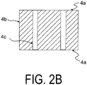
- FIGS. 2A and 2B are schematic views of a gas nozzle using the plasma resistant member of the present disclosure.
- FIG. 2A is a perspective view and FIG. 2B is a cross-sectional view taken along the line A1-A1 in FIG. 2A .
- the gas nozzle 4 is formed in, for example, a columnar shape such as a cylinder or a prism, and a plurality of (four in the example illustrated in FIG. 2A ) supply holes 11 for guiding gas are provided along an axial center of the gas nozzle 4.
- An end surface 4a, an outer peripheral surface 4b, and an inner peripheral surface 4c of the gas nozzle 4 are exposed to plasma.
- FIG. 3 is a schematic view of a window using the plasma resistant member of the present disclosure.
- the window 12 has a first surface 12a and a second surface facing each other, and the first surface 12a is exposed to plasma.
- a single crystal yttrium•aluminum•garnet has a cubic system crystal structure and has a crystal orientation such as a ⁇ 100 ⁇ plane and a ⁇ 111 ⁇ plane.
- the YAG is a material having high plasma resistance, but particularly, the present inventor has found that the ⁇ 100 ⁇ plane has excellent plasma resistance by the following experiments.
- a reactive ion etching device (RIE device) was used to irradiate a sample with CF 4 plasma, and etch depths (etching rates) were compared. It was found that etching depths of alumina ceramics, (100) single crystal YAG, (111) single crystal YAG, and yttrium ceramic are 0.61 ⁇ m, 0.16 ⁇ m, 0.20 ⁇ m, and 0.13 ⁇ m, respectively, the plasma resistance of the single crystal YAG is higher than that of the alumina ceramic and comparable to that of the yttrium ceramic, and particularly, the single crystal YAG having a ⁇ 100 ⁇ plane has excellent plasma resistance.
- RIE device reactive ion etching device
- the plasma resistant member of the present disclosure can have both high strength and corrosion resistance.
- a surface exposed to plasma is formed from a single crystal YAG having a ⁇ 100 ⁇ plane.
- At least the first surface 12a exposed to plasma is formed from a single crystal YAG having a ⁇ 100 ⁇ plane.
- a surface required to have the highest plasma corrosion resistance among the surfaces exposed to plasma is formed from a single crystal YAG having a ⁇ 100 ⁇ plane.
- the end surface 4a of the gas nozzle 4 is used as a ⁇ 100 ⁇ plane.
- the inner circumferential surface 4c may also be used as a ⁇ 100 ⁇ plane.
- the outer peripheral surface 4b may also be used as a ⁇ 100 ⁇ plane.
- a surface exposed to plasma is formed from a single crystal YAG.
- corrosion resistance is improved by reducing the porosity and surface roughness of a member.
- a single crystal has high corrosion resistance because it has smaller and fewer pores (or no pores) as compared to ceramics (polycrystals).
- crystal grain boundaries have poor crystallinity and are easily etched as compared to the inside of crystal grains, but since the single crystal has no crystal grain boundaries, the corrosion resistance is high.
- there are no crystal grain boundaries and small (few) pores surface roughness is easily reduced.
- there are no crystal grain boundaries and small pores, and few (or no) pores particles are less likely to be generated.
- the single crystal YAG is a plasma resistant member having excellent corrosion resistance and less generation of particles.
- the crystal surface of the YAG used for the plasma resistant member of the present disclosure may have an offset angle of ⁇ 10° or less, particularly preferably ⁇ 5° or less from a ⁇ 100 ⁇ plane.
- the offset angle is 10° or less, plasma resistance comparable to that of the ⁇ 100 ⁇ plane can be expected.
- the end surface 4a which has an axial direction of ⁇ 100> and is most exposed to plasma, is a ⁇ 100 ⁇ plane, and as in the example of FIG. 2A or the example of FIG.
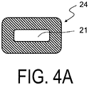
- the shape of a cross-section of at least one of an inner peripheral surface (for example, an inner peripheral surface of the supply hole 11 of the gas nozzle 4 or an inner peripheral surface 21 of a gas nozzle 24) or an outer peripheral surface of the member may be rectangular, particularly preferably square, the cross-section being perpendicular to an axis.
- each inner peripheral surface or each outer peripheral surface is an equivalent surface and corrosion resistance and various physical properties of each surface are equal, it is suitable as a corrosion resistant member. For example, deformation due to anisotropy of a thermal expansion rate is less likely to occur.
- the end surface 4a which has an axial direction of ⁇ 100> and is most exposed to plasma, is a ⁇ 100 ⁇ plane, and as illustrated in FIG. 4B , when the shape (outer shape, inner shape, and arrangement of a through-hole 31) of a cross-section of a member (gas nozzle 34) has four-fold symmetry, the cross-section being perpendicular to an axis, since various physical properties in the cross-section are relatively isotropic, it is suitable as a corrosion resistant member.
- the plasma treatment device component and the plasma treatment device of the present disclosure use the plasma resistant member having the above configuration.
- the ingot of the single crystal YAG can be produced by using a Czochralski (CZ) method, for example.
- a raw material which is obtained by mixing high-purity (for example, 4N or more) yttria powder and alumina powder, or a polycrystalline YAG, which is obtained by calcining the raw material, is filled in a crucible made of high melting point metal such as iridium, and is heated and melted, and a seed crystal is immersed in a melt and then is pulled up at a predetermined pulling speed and rotation speed, so that a single crystal having a cylindrical straight body can be grown.
- a high-purity (for example, 4N or more) single crystal having a desired crystal orientation can be produced.
- a rod-shaped, tubular, or plate-shaped single crystal YAG can be produced by using an edge-defined film-fed growth (EFG) method, for example.
- a raw material which is obtained by mixing high-purity (for example, 4N or more) yttria powder and alumina powder, or a polycrystalline YAG, which is obtained by calcining the raw material, is filled in a crucible provided with a mold having a slit and made of high melting point metal such as iridium, and is heated and melted, and a seed crystal is immersed in a melt supplied to an upper surface of the mold via the slit and then is pulled up at a predetermined pulling speed, so that the rod-shaped, tubular, or plate-shaped single crystal can be grown.
- a high-purity (for example, 4N or more) single crystal having a desired crystal orientation can be produced.
- the grown ingot is cut to a desired length (thickness) by using various cutting machines such as a wire saw and an outer peripheral blade cutting machine and is processed into a desired shape and surface roughness by using various machining devices such as a machining center and a polishing device, so that a product such as a gas nozzle can be produced.
- various cutting machines such as a wire saw and an outer peripheral blade cutting machine
- machining devices such as a machining center and a polishing device
Landscapes
- Chemical & Material Sciences (AREA)
- Engineering & Computer Science (AREA)
- Materials Engineering (AREA)
- Organic Chemistry (AREA)
- Metallurgy (AREA)
- Analytical Chemistry (AREA)
- Physics & Mathematics (AREA)
- Plasma & Fusion (AREA)
- Ceramic Engineering (AREA)
- Crystallography & Structural Chemistry (AREA)
- General Chemical & Material Sciences (AREA)
- Chemical Kinetics & Catalysis (AREA)
- Mechanical Engineering (AREA)
- Manufacturing & Machinery (AREA)
- Structural Engineering (AREA)
- Inorganic Chemistry (AREA)
- Drying Of Semiconductors (AREA)
- Plasma Technology (AREA)
Abstract
Description
- The present disclosure relates to a plasma resistant member, a plasma treatment device component, and a plasma treatment device, which are used in an environment exposed to plasma.
- In the related art, a device for forming a thin film on a target by using plasma or a device for performing an etching process on the target is used in a semiconductor manufacturing process or the like. The plasma film forming device forms a thin film on the target by turning raw material gas into plasma and causing a chemical reaction. The plasma etching device etches the target by turning etching gas into plasma, chemically reacting the surface of the target with the plasma, and vaporizing the surface.
- Various plasma treatment device components such as gas nozzles, windows, and substrate mounting components are used in reaction chambers of these plasma treatment devices. As materials for these plasma treatment device components, ceramic sintered bodies such as yttrium, yttrium•aluminum•garnet (YAG), and alumina are used (PTL 1).
- When the surface of the plasma treatment device component reacts with highly reactive gas or plasma, particles may be generated from the surface. When the particles adhere to the target, since they may cause defects, the plasma treatment device component is required to have plasma resistance. Yttrium and YAG are known to have higher plasma resistance than alumina (
Patent Documents 1 and 2). - In order to reduce defects caused by particles, a plasma resistant member having further excellent plasma resistance is required.
-
- Patent Document 1:
WO 2014/119177 - Patent Document 2:
JP 10-45461 A - The present disclosure relates to a plasma resistant member in which a surface exposed to plasma is formed from a single crystal yttrium•aluminum•garnet (YAG) having a {100} plane, and a plasma treatment device component and a plasma treatment device using the plasma resistant member.
- The present disclosure relates to a plasma resistant member in which there are a plurality of surfaces exposed to plasma, at least a surface required to have the highest plasma resistance is formed from a single crystal YAG having a {100} plane, and a plasma treatment device component and a plasma treatment device using the plasma resistant member.
-
-
FIG. 1 is a schematic view of a plasma treatment device of the present disclosure. -
FIG. 2A is a schematic perspective view of a gas nozzle using a plasma resistant member of the present disclosure. -
FIG. 2B is a cross-sectional view taken along a line A1-A1 inFIG. 2A . -
FIG. 3 is a schematic view of a window using a plasma resistant member of the present disclosure. -
FIG. 4A is another example of a gas nozzle using a plasma resistant member of the present disclosure. -
FIG. 4B is another example of a gas nozzle using a plasma resistant member of the present disclosure. - Hereinafter, an embodiment of the present disclosure will be described with reference to the drawings. The present disclosure provides a plasma resistant member, a plasma treatment device component, and a plasma treatment device, which have excellent plasma resistance and less generation of particles.
- In the present specification, the plasma resistant member is a component that has corrosion resistance (hard to be etched) against plasma such as halogen-based gas.
- The plasma resistant member is used for gas supply components such as injectors, gas nozzles, and shower heads; internal monitoring components such as windows; substrate holding components such as electrostatic chucks and carrier plates, protective components such as protective tubes for thermocouples, and the like in a plasma treatment device such as a plasma film forming device or a plasma etching device.
-
FIG. 1 is a schematic cross-sectional view of a plasma treatment device using a plasma resistant member of the present disclosure. Aplasma treatment device 1 is a device that forms a thin film on atarget 5 such as a semiconductor wafer or a glass substrate or performs an etching process, thereby modifying the surface of thetarget 5. - The
plasma treatment device 1 includes areaction chamber 2 for processing thetarget 5. Inside thereaction chamber 2, agas nozzle 4 for supplying gas into thereaction chamber 2; and aholding unit 6 provided with aninternal electrode 7, such as an electrostatic chuck, are provided. Outside thereaction chamber 2, agas supply pipe 3 for supplying raw material gas to thegas nozzle 4; acoil 9 and apower supply 10 for supplying electric power for generating plasma; and abias power supply 8 connected to theinternal electrode 7 are provided. Furthermore, thereaction chamber 2 includes awindow 12 for observing the inside thereof. - The
target 5 is placed on theholding unit 6, the gas is supplied into thereaction chamber 2 via thegas nozzle 4 and is turned into plasma by electric discharge by the electric power supplied from thecoil 9 and thepower supply 10, and thetarget 5 is processed. - For example, when a thin film made of silicon dioxide (SiO2) is formed on the
substrate 5, raw material gas such as silane (SiH4) and oxygen (O2) is supplied, and when thesubstrate 5 is etched, etching gas such as halogen-based gas such as SF6, CF4, CHF3, ClF3, NF3, C3F8, C4F8, HF, Cl2, HCl, BCl3, or CCl4 is supplied. -
FIGS. 2A and2B are schematic views of a gas nozzle using the plasma resistant member of the present disclosure.FIG. 2A is a perspective view andFIG. 2B is a cross-sectional view taken along the line A1-A1 inFIG. 2A . Thegas nozzle 4 is formed in, for example, a columnar shape such as a cylinder or a prism, and a plurality of (four in the example illustrated inFIG. 2A )supply holes 11 for guiding gas are provided along an axial center of thegas nozzle 4. Anend surface 4a, an outerperipheral surface 4b, and an innerperipheral surface 4c of thegas nozzle 4 are exposed to plasma. -
FIG. 3 is a schematic view of a window using the plasma resistant member of the present disclosure. Thewindow 12 has afirst surface 12a and a second surface facing each other, and thefirst surface 12a is exposed to plasma. - A single crystal yttrium•aluminum•garnet (YAG) has a cubic system crystal structure and has a crystal orientation such as a {100} plane and a {111} plane. The YAG is a material having high plasma resistance, but particularly, the present inventor has found that the {100} plane has excellent plasma resistance by the following experiments.
- In order to evaluate the plasma resistance of various members, a reactive ion etching device (RIE device) was used to irradiate a sample with CF4 plasma, and etch depths (etching rates) were compared. It was found that etching depths of alumina ceramics, (100) single crystal YAG, (111) single crystal YAG, and yttrium ceramic are 0.61 µm, 0.16 µm, 0.20 µm, and 0.13 µm, respectively, the plasma resistance of the single crystal YAG is higher than that of the alumina ceramic and comparable to that of the yttrium ceramic, and particularly, the single crystal YAG having a {100} plane has excellent plasma resistance.
- Furthermore, since the single crystal YAG has higher strength than the yttrium ceramic, the plasma resistant member of the present disclosure can have both high strength and corrosion resistance.
- In the plasma resistant member of the present disclosure, a surface exposed to plasma is formed from a single crystal YAG having a {100} plane.
- When the plasma resistant member of the present disclosure is used for the
window 12, at least thefirst surface 12a exposed to plasma is formed from a single crystal YAG having a {100} plane. - Furthermore, in a component such as the
gas nozzle 4 having a plurality of surfaces exposed to plasma (theend surface 4a, the outerperipheral surface 4b, and the innerperipheral surface 4c in the gas nozzle 4), at least a surface required to have the highest plasma corrosion resistance among the surfaces exposed to plasma is formed from a single crystal YAG having a {100} plane. For example, in the example illustrated inFIGS. 2A and2B , theend surface 4a of thegas nozzle 4 is used as a {100} plane. Moreover, as illustrated inFIG 2A , when the cross-sectional shape of thesupply hole 11 is rectangular, the innercircumferential surface 4c may also be used as a {100} plane. Furthermore, when the outer cross-sectional shape of thegas nozzle 4 is rectangular, the outerperipheral surface 4b may also be used as a {100} plane. - In the plasma resistant member of the present disclosure, a surface exposed to plasma is formed from a single crystal YAG. As disclosed in the citation list, corrosion resistance is improved by reducing the porosity and surface roughness of a member. A single crystal has high corrosion resistance because it has smaller and fewer pores (or no pores) as compared to ceramics (polycrystals). Furthermore, in polycrystals, crystal grain boundaries have poor crystallinity and are easily etched as compared to the inside of crystal grains, but since the single crystal has no crystal grain boundaries, the corrosion resistance is high. Furthermore, since there are no crystal grain boundaries and small (few) pores, surface roughness is easily reduced. Furthermore, since there are no crystal grain boundaries and small pores, and few (or no) pores, particles are less likely to be generated. For the above reason, the single crystal YAG is a plasma resistant member having excellent corrosion resistance and less generation of particles.
- The crystal surface of the YAG used for the plasma resistant member of the present disclosure may have an offset angle of ±10° or less, particularly preferably ±5° or less from a {100} plane. When the offset angle is 10° or less, plasma resistance comparable to that of the {100} plane can be expected.
- Since the crystal structure of the YAG is a cubic system, the {100} plane has four-fold symmetry, and an equivalent plane appears when rotated by 90° about an axis perpendicular to the plane. Consequently, in a columnar or tubular member such as a gas nozzle, the
end surface 4a, which has an axial direction of <100> and is most exposed to plasma, is a {100} plane, and as in the example ofFIG. 2A or the example ofFIG. 4A , the shape of a cross-section of at least one of an inner peripheral surface (for example, an inner peripheral surface of thesupply hole 11 of thegas nozzle 4 or an innerperipheral surface 21 of a gas nozzle 24) or an outer peripheral surface of the member may be rectangular, particularly preferably square, the cross-section being perpendicular to an axis. With such a configuration, since each inner peripheral surface or each outer peripheral surface is an equivalent surface and corrosion resistance and various physical properties of each surface are equal, it is suitable as a corrosion resistant member. For example, deformation due to anisotropy of a thermal expansion rate is less likely to occur. - For the same reason, the
end surface 4a, which has an axial direction of <100> and is most exposed to plasma, is a {100} plane, and as illustrated inFIG. 4B , when the shape (outer shape, inner shape, and arrangement of a through-hole 31) of a cross-section of a member (gas nozzle 34) has four-fold symmetry, the cross-section being perpendicular to an axis, since various physical properties in the cross-section are relatively isotropic, it is suitable as a corrosion resistant member. - The plasma treatment device component and the plasma treatment device of the present disclosure use the plasma resistant member having the above configuration.
- The ingot of the single crystal YAG can be produced by using a Czochralski (CZ) method, for example. A raw material, which is obtained by mixing high-purity (for example, 4N or more) yttria powder and alumina powder, or a polycrystalline YAG, which is obtained by calcining the raw material, is filled in a crucible made of high melting point metal such as iridium, and is heated and melted, and a seed crystal is immersed in a melt and then is pulled up at a predetermined pulling speed and rotation speed, so that a single crystal having a cylindrical straight body can be grown. By appropriately selecting the crystal orientation of the seed crystal, a high-purity (for example, 4N or more) single crystal having a desired crystal orientation can be produced.
- A rod-shaped, tubular, or plate-shaped single crystal YAG can be produced by using an edge-defined film-fed growth (EFG) method, for example. A raw material, which is obtained by mixing high-purity (for example, 4N or more) yttria powder and alumina powder, or a polycrystalline YAG, which is obtained by calcining the raw material, is filled in a crucible provided with a mold having a slit and made of high melting point metal such as iridium, and is heated and melted, and a seed crystal is immersed in a melt supplied to an upper surface of the mold via the slit and then is pulled up at a predetermined pulling speed, so that the rod-shaped, tubular, or plate-shaped single crystal can be grown. By appropriately selecting the crystal orientation of the seed crystal, a high-purity (for example, 4N or more) single crystal having a desired crystal orientation can be produced.
- The grown ingot is cut to a desired length (thickness) by using various cutting machines such as a wire saw and an outer peripheral blade cutting machine and is processed into a desired shape and surface roughness by using various machining devices such as a machining center and a polishing device, so that a product such as a gas nozzle can be produced.
-
- 1 Plasma treatment device
- 2 Reaction chamber
- 3 Gas lead-in pipe
- 4 Gas nozzle
- 4a End surface
- 4b Outer peripheral surface
- 4c Inner peripheral surface
- 5 Target
- 6 Holding unit
- 7 Internal electrode
- 8 Bias power supply
- 9 Coil
- 10 Power supply
- 11 Supply hole
- 12 Window
- 12a First surface
Claims (8)
- A plasma resistant member comprising:a surface exposed to plasma,the surface being formed from a single crystal YAG having a {100} plane.
- A plasma resistant member comprising:a plurality of surfaces exposed to plasma,at least a surface required to have highest plasma resistance being formed from a single crystal YAG having a {100} plane.
- The plasma resistant member according to claim 1 or 2, whereinthe plasma resistant member is a plasma resistant member having a plate shape, anda principal plane is formed from a single crystal YAG having a {100} plane.
- The plasma resistant member according to claim 1 or 2, whereinthe plasma resistant member is a plasma resistant member having a columnar shape or a tubular shape, andat least one of an end surface, an outer peripheral surface, and an inner peripheral surface is formed from a single crystal YAG having a {100} plane.
- The plasma resistant member according to claim 4, whereinan axial direction is a <100> direction, anda shape of a cross-section of at least one of the inner peripheral surface or the outer peripheral surface is rectangular, the cross-section being perpendicular to an axis.
- The plasma resistant member according to claim 4, whereinan axial direction is a <100> direction, anda shape of a cross-section perpendicular to an axis has four-fold symmetry.
- A plasma treatment device component comprising:
the plasma resistant member according to any one of claims 1 to 6. - A plasma treatment device comprising:
the plasma resistant member according to any one of claims 1 to 6.
Applications Claiming Priority (2)
| Application Number | Priority Date | Filing Date | Title |
|---|---|---|---|
| JP2019214389 | 2019-11-27 | ||
| PCT/JP2020/043670 WO2021106871A1 (en) | 2019-11-27 | 2020-11-24 | Plasma resistant member, plasma treatment device component, and plasma treatment device |
Publications (2)
| Publication Number | Publication Date |
|---|---|
| EP4068912A1 true EP4068912A1 (en) | 2022-10-05 |
| EP4068912A4 EP4068912A4 (en) | 2023-11-22 |
Family
ID=76130469
Family Applications (1)
| Application Number | Title | Priority Date | Filing Date |
|---|---|---|---|
| EP20893806.8A Pending EP4068912A4 (en) | 2019-11-27 | 2020-11-24 | Plasma resistant member, plasma treatment device component, and plasma treatment device |
Country Status (6)
| Country | Link |
|---|---|
| US (1) | US12406831B2 (en) |
| EP (1) | EP4068912A4 (en) |
| JP (1) | JP7329619B2 (en) |
| CN (1) | CN114762090B (en) |
| TW (1) | TWI759981B (en) |
| WO (1) | WO2021106871A1 (en) |
Family Cites Families (16)
| Publication number | Priority date | Publication date | Assignee | Title |
|---|---|---|---|---|
| DE3905966A1 (en) * | 1989-02-25 | 1990-08-30 | Jenoptik Jena Gmbh | Process for growing homogeneous laser garnet crystals in accordance with the Czochralski method |
| US5851284A (en) * | 1995-11-21 | 1998-12-22 | Nippon Telegraph And Telephone Corporation | Process for producing garnet single crystal |
| JP3426845B2 (en) * | 1996-04-26 | 2003-07-14 | 京セラ株式会社 | Electrostatic chuck |
| JP3619330B2 (en) | 1996-07-31 | 2005-02-09 | 京セラ株式会社 | Components for plasma process equipment |
| JPH10236871A (en) * | 1997-02-26 | 1998-09-08 | Kyocera Corp | Plasma resistant material |
| JP4970712B2 (en) * | 2003-06-19 | 2012-07-11 | 日本碍子株式会社 | Aluminum nitride sintered body, aluminum nitride production method, and aluminum nitride evaluation method |
| US8357262B2 (en) * | 2005-08-31 | 2013-01-22 | Kyocera Corporation | Corrosion-resistant member, treatment apparatus and sample treatment method using the member, and method for manufacture of corrosion-resistant member |
| JP4996868B2 (en) * | 2006-03-20 | 2012-08-08 | 東京エレクトロン株式会社 | Plasma processing apparatus and plasma processing method |
| JP5235909B2 (en) * | 2008-02-07 | 2013-07-10 | 京セラ株式会社 | Zirconia sintered body and method for producing the same |
| JP2010070854A (en) * | 2008-08-20 | 2010-04-02 | Kyocera Corp | Corrosion resistant member and semiconductor fabrication apparatus using the same |
| JP2011071323A (en) * | 2009-09-25 | 2011-04-07 | Koito Mfg Co Ltd | Semiconductor element, and method of manufacturing the same |
| US20120103519A1 (en) * | 2010-10-25 | 2012-05-03 | Greene, Tweed Of Delaware, Inc. | Plasma Etch Resistant, Highly Oriented Yttria Films, Coated Substrates and Related Methods |
| US9790596B1 (en) | 2013-01-30 | 2017-10-17 | Kyocera Corporation | Gas nozzle and plasma device employing same |
| JP5768159B2 (en) * | 2014-03-14 | 2015-08-26 | 株式会社小糸製作所 | Manufacturing method of semiconductor device |
| CN104229857B (en) * | 2014-08-14 | 2016-10-12 | 中国科学院上海硅酸盐研究所 | A kind of preparation method of the YAG crystallite of morphology controllable |
| CN109923092B (en) * | 2016-12-20 | 2022-04-01 | 三井金属矿业株式会社 | Rare earth oxyfluoride sintered compact and method for producing same |
-
2020
- 2020-11-24 CN CN202080082042.8A patent/CN114762090B/en active Active
- 2020-11-24 WO PCT/JP2020/043670 patent/WO2021106871A1/en not_active Ceased
- 2020-11-24 US US17/778,717 patent/US12406831B2/en active Active
- 2020-11-24 EP EP20893806.8A patent/EP4068912A4/en active Pending
- 2020-11-24 JP JP2021561420A patent/JP7329619B2/en active Active
- 2020-11-27 TW TW109141738A patent/TWI759981B/en active
Also Published As
| Publication number | Publication date |
|---|---|
| JPWO2021106871A1 (en) | 2021-06-03 |
| US20230019508A1 (en) | 2023-01-19 |
| EP4068912A4 (en) | 2023-11-22 |
| US12406831B2 (en) | 2025-09-02 |
| JP7329619B2 (en) | 2023-08-18 |
| CN114762090A (en) | 2022-07-15 |
| CN114762090B (en) | 2025-11-04 |
| WO2021106871A1 (en) | 2021-06-03 |
| TWI759981B (en) | 2022-04-01 |
| TW202125630A (en) | 2021-07-01 |
Similar Documents
| Publication | Publication Date | Title |
|---|---|---|
| CN101903558B (en) | Corrosion-resistant, yttrium-containing metal plasma chamber components with oxide coating | |
| US6861122B2 (en) | Ceramic member with fine protrusions on surface and method of producing the same | |
| KR101273209B1 (en) | Free-standing silicon carbide articles formed by chemical vapor deposition and methods for their manufacture | |
| JP7112491B2 (en) | Ceramic sintered bodies and members for plasma processing equipment | |
| TWI769013B (en) | Ceramic sintered body comprising magnesium aluminate spinel | |
| JP7644812B2 (en) | Composite substrate, method for producing the composite substrate, and method for producing the gallium oxide crystal film | |
| US20070084398A1 (en) | Monocrystalline diamond layer and method for the production thereof | |
| JP2000191370A (en) | Member for treatment chamber | |
| US12406831B2 (en) | Plasma resistant member, plasma treatment device component, and plasma treatment device | |
| JP7223669B2 (en) | Corrosion-resistant materials, parts for semiconductor manufacturing equipment, and semiconductor manufacturing equipment | |
| WO2012165334A1 (en) | CaF2 POLYCRYSTALLINE BODY, FOCUS RING, PLASMA TREATMENT APPARATUS, AND METHOD FOR PRODUCING CaF2 POLYCRYSTALLINE BODY | |
| CN103668460A (en) | Group 13 nitride crystal, said crystal substrate, and said crystal preparation method | |
| TWI897894B (en) | Single crystal metal oxide plasma chamber component and the method of forming the same | |
| WO2021020502A1 (en) | Gas nozzle and plasma processing device using same | |
| JP7470222B2 (en) | Gas nozzle manufacturing method | |
| JP7329610B2 (en) | Member for plasma processing apparatus, manufacturing method thereof, and plasma processing apparatus | |
| WO2026029848A1 (en) | Apparatus and method for growth of gallium oxide crystal with an offcut | |
| WO2025250905A1 (en) | Apparatus and method for growth of gallium oxide crystal with an offcut | |
| JP3195093B2 (en) | Method of forming diamond film |
Legal Events
| Date | Code | Title | Description |
|---|---|---|---|
| STAA | Information on the status of an ep patent application or granted ep patent |
Free format text: STATUS: THE INTERNATIONAL PUBLICATION HAS BEEN MADE |
|
| PUAI | Public reference made under article 153(3) epc to a published international application that has entered the european phase |
Free format text: ORIGINAL CODE: 0009012 |
|
| STAA | Information on the status of an ep patent application or granted ep patent |
Free format text: STATUS: REQUEST FOR EXAMINATION WAS MADE |
|
| 17P | Request for examination filed |
Effective date: 20220520 |
|
| AK | Designated contracting states |
Kind code of ref document: A1 Designated state(s): AL AT BE BG CH CY CZ DE DK EE ES FI FR GB GR HR HU IE IS IT LI LT LU LV MC MK MT NL NO PL PT RO RS SE SI SK SM TR |
|
| DAV | Request for validation of the european patent (deleted) | ||
| DAX | Request for extension of the european patent (deleted) | ||
| P01 | Opt-out of the competence of the unified patent court (upc) registered |
Effective date: 20230505 |
|
| REG | Reference to a national code |
Ref country code: DE Ref legal event code: R079 Free format text: PREVIOUS MAIN CLASS: H05H0001460000 Ipc: C23C0016440000 |
|
| A4 | Supplementary search report drawn up and despatched |
Effective date: 20231019 |
|
| RIC1 | Information provided on ipc code assigned before grant |
Ipc: C30B 29/28 20060101ALI20231013BHEP Ipc: C30B 15/34 20060101ALI20231013BHEP Ipc: C23C 16/455 20060101ALI20231013BHEP Ipc: C23C 16/44 20060101AFI20231013BHEP |