EP4068635B1 - Dualmodus-durchschnittsleistungsverfolgungssteuergerät - Google Patents
Dualmodus-durchschnittsleistungsverfolgungssteuergerät Download PDFInfo
- Publication number
- EP4068635B1 EP4068635B1 EP22157582.2A EP22157582A EP4068635B1 EP 4068635 B1 EP4068635 B1 EP 4068635B1 EP 22157582 A EP22157582 A EP 22157582A EP 4068635 B1 EP4068635 B1 EP 4068635B1
- Authority
- EP
- European Patent Office
- Prior art keywords
- circuit
- mode
- signal
- apt
- loop filter
- Prior art date
- Legal status (The legal status is an assumption and is not a legal conclusion. Google has not performed a legal analysis and makes no representation as to the accuracy of the status listed.)
- Active
Links
Images




Classifications
-
- H—ELECTRICITY
- H03—ELECTRONIC CIRCUITRY
- H03F—AMPLIFIERS
- H03F1/00—Details of amplifiers with only discharge tubes, only semiconductor devices or only unspecified devices as amplifying elements
- H03F1/02—Modifications of amplifiers to raise the efficiency, e.g. gliding Class A stages, use of an auxiliary oscillation
- H03F1/0205—Modifications of amplifiers to raise the efficiency, e.g. gliding Class A stages, use of an auxiliary oscillation in transistor amplifiers
- H03F1/0211—Modifications of amplifiers to raise the efficiency, e.g. gliding Class A stages, use of an auxiliary oscillation in transistor amplifiers with control of the supply voltage or current
- H03F1/0216—Continuous control
- H03F1/0233—Continuous control by using a signal derived from the output signal, e.g. bootstrapping the voltage supply
-
- H—ELECTRICITY
- H04—ELECTRIC COMMUNICATION TECHNIQUE
- H04B—TRANSMISSION
- H04B1/00—Details of transmission systems, not covered by a single one of groups H04B3/00 - H04B13/00; Details of transmission systems not characterised by the medium used for transmission
- H04B1/02—Transmitters
- H04B1/04—Circuits
-
- G—PHYSICS
- G05—CONTROLLING; REGULATING
- G05F—SYSTEMS FOR REGULATING ELECTRIC OR MAGNETIC VARIABLES
- G05F1/00—Automatic systems in which deviations of an electric quantity from one or more predetermined values are detected at the output of the system and fed back to a device within the system to restore the detected quantity to its predetermined value or values, i.e. retroactive systems
- G05F1/66—Regulating electric power
-
- H—ELECTRICITY
- H03—ELECTRONIC CIRCUITRY
- H03F—AMPLIFIERS
- H03F1/00—Details of amplifiers with only discharge tubes, only semiconductor devices or only unspecified devices as amplifying elements
- H03F1/02—Modifications of amplifiers to raise the efficiency, e.g. gliding Class A stages, use of an auxiliary oscillation
- H03F1/0205—Modifications of amplifiers to raise the efficiency, e.g. gliding Class A stages, use of an auxiliary oscillation in transistor amplifiers
- H03F1/0211—Modifications of amplifiers to raise the efficiency, e.g. gliding Class A stages, use of an auxiliary oscillation in transistor amplifiers with control of the supply voltage or current
- H03F1/0216—Continuous control
- H03F1/0222—Continuous control by using a signal derived from the input signal
- H03F1/0227—Continuous control by using a signal derived from the input signal using supply converters
-
- H—ELECTRICITY
- H03—ELECTRONIC CIRCUITRY
- H03F—AMPLIFIERS
- H03F1/00—Details of amplifiers with only discharge tubes, only semiconductor devices or only unspecified devices as amplifying elements
- H03F1/02—Modifications of amplifiers to raise the efficiency, e.g. gliding Class A stages, use of an auxiliary oscillation
- H03F1/0205—Modifications of amplifiers to raise the efficiency, e.g. gliding Class A stages, use of an auxiliary oscillation in transistor amplifiers
- H03F1/0211—Modifications of amplifiers to raise the efficiency, e.g. gliding Class A stages, use of an auxiliary oscillation in transistor amplifiers with control of the supply voltage or current
- H03F1/0216—Continuous control
- H03F1/0222—Continuous control by using a signal derived from the input signal
-
- H—ELECTRICITY
- H03—ELECTRONIC CIRCUITRY
- H03F—AMPLIFIERS
- H03F3/00—Amplifiers with only discharge tubes or only semiconductor devices as amplifying elements
- H03F3/20—Power amplifiers, e.g. Class B amplifiers, Class C amplifiers
- H03F3/21—Power amplifiers, e.g. Class B amplifiers, Class C amplifiers with semiconductor devices only
-
- H—ELECTRICITY
- H03—ELECTRONIC CIRCUITRY
- H03F—AMPLIFIERS
- H03F3/00—Amplifiers with only discharge tubes or only semiconductor devices as amplifying elements
- H03F3/20—Power amplifiers, e.g. Class B amplifiers, Class C amplifiers
- H03F3/21—Power amplifiers, e.g. Class B amplifiers, Class C amplifiers with semiconductor devices only
- H03F3/217—Class D power amplifiers; Switching amplifiers
- H03F3/2175—Class D power amplifiers; Switching amplifiers using analogue-digital or digital-analogue conversion
-
- H—ELECTRICITY
- H03—ELECTRONIC CIRCUITRY
- H03M—CODING; DECODING; CODE CONVERSION IN GENERAL
- H03M1/00—Analogue/digital conversion; Digital/analogue conversion
- H03M1/66—Digital/analogue converters
-
- H—ELECTRICITY
- H03—ELECTRONIC CIRCUITRY
- H03F—AMPLIFIERS
- H03F2200/00—Indexing scheme relating to amplifiers
- H03F2200/102—A non-specified detector of a signal envelope being used in an amplifying circuit
-
- H—ELECTRICITY
- H03—ELECTRONIC CIRCUITRY
- H03F—AMPLIFIERS
- H03F2200/00—Indexing scheme relating to amplifiers
- H03F2200/105—A non-specified detector of the power of a signal being used in an amplifying circuit
-
- H—ELECTRICITY
- H03—ELECTRONIC CIRCUITRY
- H03F—AMPLIFIERS
- H03F2200/00—Indexing scheme relating to amplifiers
- H03F2200/165—A filter circuit coupled to the input of an amplifier
-
- H—ELECTRICITY
- H03—ELECTRONIC CIRCUITRY
- H03F—AMPLIFIERS
- H03F2200/00—Indexing scheme relating to amplifiers
- H03F2200/451—Indexing scheme relating to amplifiers the amplifier being a radio frequency amplifier
-
- H—ELECTRICITY
- H03—ELECTRONIC CIRCUITRY
- H03F—AMPLIFIERS
- H03F3/00—Amplifiers with only discharge tubes or only semiconductor devices as amplifying elements
- H03F3/189—High-frequency amplifiers, e.g. radio frequency amplifiers
-
- H—ELECTRICITY
- H04—ELECTRIC COMMUNICATION TECHNIQUE
- H04B—TRANSMISSION
- H04B1/00—Details of transmission systems, not covered by a single one of groups H04B3/00 - H04B13/00; Details of transmission systems not characterised by the medium used for transmission
- H04B1/02—Transmitters
- H04B1/04—Circuits
- H04B2001/0408—Circuits with power amplifiers
- H04B2001/045—Circuits with power amplifiers with means for improving efficiency
Definitions
- the technology of the disclosure relates generally to average power tracking (APT) in wireless communication devices.
- APT average power tracking
- Mobile communication devices have become increasingly common in current society. The prevalence of these mobile communication devices is driven in part by the many functions that are now enabled on such devices. Increased processing capabilities in such devices means that mobile communication devices have evolved from being pure communication tools into sophisticated mobile multimedia centers that enable enhanced user experiences.
- 5G-NR fifth-generation new-radio
- Wi-Fi Wi-Fi
- LTE long-term evolution
- 5G-NR fifth-generation new-radio
- 5G-NR implements a rigorous power control scheme with frequent changes to transmission power levels.
- the frequent changes in transmission power levels in turn necessitate the ability to change the output of power amplifier arrays quickly, which is typically done through some form of envelope tracking (ET) or average power tracking (APT).
- ET and APT approaches frequent power level changes necessitate frequently changing control signals sent to the power amplifier arrays.
- the envelope tracking system discloses envelope tracking as a means of solving inefficiencies in wideband power amplifiers in the context of wireless telecom and other base station transmitters.
- US 2016/094192 A1 discloses a variable load power amplifier that improves the performance of a power amplifier that provides both envelope tracking and average power tracking.
- US 10 622 898 B1 discloses techniques for regulating voltage supplied to a power amplifier.
- a dual-mode average power tracking (APT) controller In a first mode, the APT controller operates to move the control voltage quickly without concern for ripple or ringing. When this coarse adjustment takes the control voltage to within a desired margin of a target, the controller may switch to a second mode, where the APT controller more slowly approaches the target, but has reduced ringing or ripples. The mode is changed by changing resistance and capacitance values in a loop filter within the APT circuit.
- a pulse shaper circuit may inject a pulse to force the control voltage to change more rapidly. By switching modes in this fashion, the control voltage may quickly reach a desired target, and then remain in the second mode during a transmission time slot such that the control voltage is clean throughout.
- an APT circuit comprises a digital-to-analog converter (DAC).
- the DAC comprises a change signal output configured to provide a change signal indicative of a needed change in a voltage control signal (Vcc) and a target control voltage signal output.
- the APT circuit also comprises a transition management circuit coupled to the change signal output and configured to receive the change signal and comprising a mode output configured to provide a mode signal based on the change signal.
- the APT circuit also comprises a loop filter coupled to the target control voltage signal output and the mode output. A change in the mode signal causes the loop filter to switch between a first mode and a second mode and the loop filter is configured to provide a signal.
- the APT circuit also comprises output circuitry configured to provide the Vcc based on the signal from the loop filter.
- a dual-mode average power tracking (APT) controller In a first mode, the APT controller operates to move the control voltage quickly without concern for ripple or ringing. When this coarse adjustment takes the control voltage to within a desired margin of a target, the controller may switch to a second mode, where the APT controller more slowly approaches the target, but has reduced ringing or ripples. The mode is changed by changing resistance and capacitance values in a loop filter within the APT circuit.
- a pulse shaper circuit may inject a pulse to force the control voltage to change more rapidly. By switching modes in this fashion, the control voltage may quickly reach a desired target, and then remain in the second mode during a transmission time slot such that the control voltage is clean throughout.
- FIG. 1 illustrates a block diagram of a conventional APT circuit 10.
- the APT circuit 10 includes a digital-to-analog converter (DAC) 12.
- the DAC 12 includes an input 14 (input 14 may be a pin or a node as is well understood) that receives a digital signal 16 from an envelope tracking (ET) circuit (not shown).
- the DAC 12 converts the digital signal 16 to an analog target control voltage signal 18.
- An adder 20 adds the target control voltage signal 18 to an inverted (negative) feedback signal 22.
- the adder 20 is coupled to a loop filter 24.
- the loop filter 24 may also include a controller (not shown) and/or an error amplifier (also not shown).
- a signal 26 from the adder 20 is filtered by the loop filter 24 to produce a signal 28.
- the signal 28 is provided to a switch control circuit 30, which turns on and off switches in a switch array circuit 32 based on the signal 28.
- the switch control circuit 30 represents a function that sequences the closing of the various power switches in the switch array circuit 32 to control the output of the switch array circuit 32.
- the switch control circuit 30 may be a pulse width modulation (PWM) modulator.
- PWM pulse width modulation
- the output of the switch array circuit 32 is filtered by an inductor 34 and a capacitor 36 to provide a voltage control signal 38 (also referred to as Vcc), which is used to control power amplifiers in a transmitter (not shown).
- the voltage control signal 38 is also provided to a feedback circuit 40, which provides the feedback signal 22 to the adder 20.
- New cellular standards like 5G changed the RF output power control scheme such that power changes are frequent, especially compared to previous cellular standards.
- 5G-NR may have a power change occurring within 8.3 microseconds ( ⁇ s) with a 120 kilohertz (kHz) sub-carrier spacing (SCS). Consequently, the power amplifier voltage must settle extremely fast when there is a power level change.
- ⁇ s 8.3 microseconds
- kHz sub-carrier spacing
- APT where Vcc is only supposed to change when power is requested to change, such fast transitions are a challenge while having stable Vcc during unchanging slots.
- the limit on how fast Vcc can change is the capacitance of the capacitor 36 along with a rate of charging for the capacitor (i.e., how quickly can current be "poured into” the capacitor 36).
- the charging rate is a function of the inductor 34, with the rate increasing as the inductance of the inductor 34 decreases. Further, the more voltage across the inductor 34, the faster the current change rate.
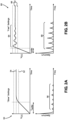
- Using traditional systems may result in a slow settle as seen in Figure 2A where graph 50 shows Vcc requiring time Tsettle to get to a lower threshold 52 and even more time to get to the final target level 54.
- the slow approach to the final target level 54 results in relatively low ringing in the frequency domain as evidenced by spurs 56.
- Exemplary aspects of the present disclosure adopt a two-mode approach, where a first fast mode, but likely ringing- or ripple-inducing, circuit is used to make a coarse adjustment that quickly changes Vcc to a value within a predefined threshold of a target Vcc value, and a second slow mode is used to provide a clean non-ringing, but comparatively slow, fine adjustment to Vcc that changes Vcc to the final target Vcc value and holds Vcc at this final target cleanly for the desired duration (e.g., in the "slot").
- the loop filter circuit is changed.
- the resistance(s) and/or capacitance(s) within the loop filter are changed.
- a pulse shaper circuit may be used to inject a hard pulse form to assist in changing the input to the switch control circuit to the desired target value.
- Figure 3 illustrates an APT circuit 80 that includes a DAC 82.
- the DAC 82 includes an input 84 (which may be a pin or a node as is well understood) that receives a digital signal 86 from an ET circuit (not shown).
- the DAC 82 converts the digital signal 86 to an analog target control voltage signal 88 at a target control voltage signal output 89 (which may also be a pin or a node).
- An adder 90 (equivalently an adder circuit) adds the target control voltage signal 88 to an inverted (negative) feedback signal 92.
- the adder 90 is coupled to a loop filter 94, and thus, the loop filter 94 is coupled to the target control voltage signal output 89 indirectly.
- the loop filter 94 may also include a controller (not shown) and/or an error amplifier (also not shown).
- a signal 96 from the adder 90 is filtered by the loop filter 94 to produce a signal 98.
- the signal 98 is provided to a switch control circuit 100, which turns on and off switches in a switch array circuit 102 based on the signal 98.
- the switch control circuit 100 represents a function that sequences the closing of the various power switches in the switch array circuit 102 to control the output of the switch array circuit 102.
- the switch control circuit 100 may be a PWM modulator.
- the output of the switch array circuit 102 is filtered by an inductor 104 and a capacitor 106 to provide a voltage control signal 108 (also referred to as Vcc) at an output 109 (which may also be a pin or a node).
- the voltage control signal 108 is used to control power amplifiers in a transmitter (not shown).
- the voltage control signal 108 is also provided to a feedback circuit 110, which provides the feedback signal 92 to the adder 90.
- the switch control circuit 100, the switch array circuit 102, and the filter formed by the inductor 104 and the capacitor 106 may be considered output circuitry that is configured to provide the voltage control signal 108 based on the signal 98 at the output 109.
- the constituent elements of the output circuitry may vary without departing from the scope of the present disclosure.
- the DAC 82 also includes a change signal output 112 (which may also be a pin or node) that provides a signal 114 indicative of a change in state of the DAC 82.
- the signal 114 is generated each time there is a change in the state of the DAC 82.
- the signal 114 may be generated only when the change in state exceeds a predefined threshold.
- the signal 114 may include information not merely relating to the existence of a change in state, but also a magnitude and direction of the change.
- the change in state of the DAC 82 is indicative of a needed change in the voltage control signal 108, and thus, small changes needed to the voltage control signal 108 may not need to implement the fast mode of the present disclosure.
- a transition management circuit 116 is coupled to the change signal output 112 to receive the signal 114.
- the transition management circuit 116 is configured to provide a mode signal 118 to the loop filter 94.
- the loop filter 94 may change between a first mode (i.e., a fast mode) and a second mode (i.e., a slow mode).
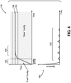
- Figure 4 illustrates the difference in modes. Specifically, graph 130 shows Vcc rapidly climbing in the first mode 132 until a threshold 134 is reached, at which time the mode signal 118 causes the loop filter 94 to change the second mode 136 which allows Vcc to settle slowly to the target value 138, effectively without ripple and as evidenced by the spectrum graph 140, with little or no problematic ringing 142.
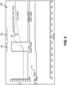
- Exemplary test results comparing the dual-mode approach of the present disclosure to conventional systems are shown in graph 150 of Figure 5 , where the first mode 132 lasts from approximately 65.25 ⁇ s to 66 ⁇ s (or about 0.75 ⁇ s) after which the second mode 136 begins.
- Vcc 152 reaches a zone close to the target Vcc value much faster than the Vcc baseline 154 of the conventional approach.
- the signal 114 from the DAC 82 is also included to show the transition relative to the change in the DAC 82.
- Figure 6 provides an alternate aspect where a pulse shaper circuit 160 is added to the APT circuit 80'.
- the pulse shaper circuit 160 is coupled to an adder 162 (equivalently an adder circuit or second adder circuit) positioned between the loop filter 94 and the switch control circuit 100.
- the pulse shaper circuit 160 may inject voltage spurs or other pulse signals 164 (positive or negative) through the adder 162 to facilitate more rapid changes in Vcc.
- the pulse shaper circuit 160 is controlled by the transition management circuit 116 and may have a programmable duration period. That is, the height and/or length of the pulse to be injected may be varied.
- the programmable duration period may be a function of a battery voltage and/or a voltage step change. For example, if there is a relatively small voltage step change of one volt (1 V), a smaller (magnitude and/or duration) pulse may be applied than if there were a relatively larger step change of three volts (3 V).
- loop filter 94 may take any number of forms including, for example, type I, II, or III loop filters, most such filters include one or more resistors and one or more capacitors. Exemplary aspects of the present disclosure change these resistances and capacitances to change between the first mode and the second mode.
- variable resistors are used as illustrated in Figure 7A .
- switches are used to switch between resistors and/or capacitors having different values as illustrated in Figure 7B .
- Figure 7A illustrates a loop filter 94A, with variable capacitors 180(1)-180(N) and variable resistors 182(2)-182(N).
- the mode signal 118 causes the values of the variable elements to be changed.
- Figure 7B illustrates a loop filter 94B with switches 190(1)-190(N) that may be used to switch between different capacitances and resistances. Note that as illustrated, switches 190(N) allow for just the resistances to be switched, while leaving the capacitance associated therewith unchanged. Other switching arrangements are possible. As with the loop filter 94A, the mode signal 118 causes the switches 190(1)-190(N) to open and close so as to switch between the first mode and the second mode.
Landscapes
- Engineering & Computer Science (AREA)
- Power Engineering (AREA)
- Theoretical Computer Science (AREA)
- Computer Networks & Wireless Communication (AREA)
- General Physics & Mathematics (AREA)
- Radar, Positioning & Navigation (AREA)
- Automation & Control Theory (AREA)
- Electromagnetism (AREA)
- Physics & Mathematics (AREA)
- Signal Processing (AREA)
- Amplifiers (AREA)
- Filters And Equalizers (AREA)
- Transmitters (AREA)
- Analogue/Digital Conversion (AREA)
- Networks Using Active Elements (AREA)
- Electronic Switches (AREA)
Claims (15)
- Durchschnittsleistungsverfolgungsschaltung, APT-Schaltung, (80; 80'), die Folgendes umfasst:
einen Digital/Analog-Umsetzer, DAC (82), der Folgendes umfasst:einen Änderungssignalausgang (112), der konfiguriert ist, ein Änderungssignal (114) zu liefern, das eine benötigte Änderung eines Spannungssteuersignals, Vcc, (108) angibt; undeinen Zielsteuerspannungssignalausgang (89);eine Übergangsmanagementschaltung (116), die an den Änderungssignalausgang gekoppelt ist und konfiguriert ist, das Änderungssignal (114) zu empfangen, und einen Modusausgang umfasst, der konfiguriert ist, ein Modussignal (118) auf der Grundlage des Änderungssignals (114) zu liefern;ein Schleifenfilter (94), das an den Zielsteuerspannungssignalausgang und den Modusausgang gekoppelt ist, wobei eine Änderung des Modussignals verursacht, dass das Schleifenfilter zwischen einem ersten Modus und einem zweiten Modus umschaltet, und das Schleifenfilter konfiguriert ist, ein Signal zu liefern; undeine Ausgangsschaltungsanordnung (100, 102), die konfiguriert ist, das Vcc auf der Grundlage des Signals vom Schleifenfilter zu liefern. - APT-Schaltung nach Anspruch 1, wobei die Ausgangsschaltungsanordnung Folgendes umfasst:eine Schaltersteuerschaltung (100), die an das Schleifenfilter und die Übergangsmanagementschaltung gekoppelt ist, wobei die Schaltersteuerschaltung konfiguriert ist, das Signal vom Schleifenfilter zu empfangen; undeine Schalteranordnungsschaltung (102), die mehrere Leistungsschalter umfasst, die an die Schaltersteuerschaltung gekoppelt sind, wobei die Schaltersteuerschaltung konfiguriert ist, auf der Grundlage des Signals zu steuern, welche der mehreren Leistungsschalter offen sind und welche geschlossen sind.
- APT-Schaltung nach Anspruch 1, die ferner Folgendes umfasst:eine Addiererschaltung (90), die zwischen dem DAC und dem Schleifenfilter positioniert ist; undeine Rückkopplungsschaltung (110), die an die Addiererschaltung gekoppelt ist.
- APT-Schaltung nach Anspruch 1, die ferner eine Pulsformerschaltung (160) umfasst, die an die Übergangsmanagementschaltung und den Zielsteuerspannungssignalausgang gekoppelt ist.
- APT-Schaltung nach Anspruch 4, die ferner eine zweite Addiererschaltung (162) umfasst, die an das Schleifenfilter und die Pulsformerschaltung gekoppelt ist, wobei die Pulsformerschaltung konfiguriert ist, ein Pulssignal (164) zu liefern, das durch die zweite Addiererschaltung zum Signal vom Schleifenfilter addiert wird.
- APT-Schaltung nach Anspruch 1, wobei der erste Modus einen schnellen Modus umfasst und der zweite Modus einen langsamen Modus umfasst und der schnelle Modus das Signal schneller ändert als der langsame Modus.
- APT-Schaltung nach Anspruch 1, wobei das Schleifenfilter konfiguriert ist, zu arbeiten, wie folgt: mit einem ersten Widerstand im ersten Modus und einem zweiten Widerstand im zweiten Modus, wobei der erste Widerstand nicht gleich dem zweiten Widerstand ist; oder mit einer ersten Kapazität im ersten Modus und einer zweiten Kapazität im zweiten Modus, wobei die erste Kapazität nicht gleich der zweiten Kapazität ist.
- APT-Schaltung nach Anspruch 1, wobei das Schleifenfilter Folgendes umfasst: mindestens einen veränderbaren Widerstand oder mindestens einen veränderbaren Kondensator.
- APT-Schaltung nach Anspruch 1, wobei das Schleifenfilter Folgendes umfasst: mindestens zwei Widerstände und einen Schalter, der konfiguriert ist, einen oder den weiteren der mindestens zwei Widerstände auf der Grundlage des Signals zu verbinden; oder mindestens zwei Kondensatoren und einen Schalter, der konfiguriert ist, einen oder den weiteren der mindestens zwei Kondensatoren auf der Grundlage des Signals zu verbinden.
- APT nach Anspruch 1, wobei die Übergangsmanagementschaltung konfiguriert ist, nach etwa einer Mikrosekunde im ersten Modus Modi mit dem Modussignal vom ersten Modus zum zweiten Modus zu ändern.
- APT nach Anspruch 1, wobei die Übergangsmanagementschaltung konfiguriert ist, vor etwa vier Mikrosekunden im ersten Modus Modi mit dem Modussignal vom ersten Modus zum zweiten Modus zu ändern.
- APT nach Anspruch 1, wobei der DAC ferner einen Eingang umfasst, der konfiguriert ist, ein digitales Zielspannungssignal zu empfangen, und der DAC konfiguriert ist, ein Änderungssignal am Änderungssignalausgang zu liefern, wenn das digitale Zielspannungssignal sich ändert.
- APT nach Anspruch 1, wobei der DAC ferner einen Eingang umfasst, der konfiguriert ist, ein digitales Zielspannungssignal zu empfangen, und der DAC konfiguriert ist, ein Änderungssignal am Änderungssignalausgang zu liefern, wenn das digitale Zielspannungssignal sich um mehr als einen vordefinierten Schwellenwert ändert.
- APT-Schaltung nach Anspruch 4, wobei die Pulsformerschaltung konfiguriert ist, einen Zeitraum programmierbarer Dauer aufzuweisen.
- APT-Schaltung nach Anspruch 14, wobei der Zeitraum programmierbarer Dauer eine Funktion von Folgendem ist: einer Batteriespannung oder einer Spannungsstufenänderung.
Applications Claiming Priority (1)
| Application Number | Priority Date | Filing Date | Title |
|---|---|---|---|
| US17/215,132 US11545937B2 (en) | 2021-03-29 | 2021-03-29 | Dual-mode average power tracking (APT) controller |
Publications (2)
| Publication Number | Publication Date |
|---|---|
| EP4068635A1 EP4068635A1 (de) | 2022-10-05 |
| EP4068635B1 true EP4068635B1 (de) | 2024-10-02 |
Family
ID=80736089
Family Applications (1)
| Application Number | Title | Priority Date | Filing Date |
|---|---|---|---|
| EP22157582.2A Active EP4068635B1 (de) | 2021-03-29 | 2022-02-18 | Dualmodus-durchschnittsleistungsverfolgungssteuergerät |
Country Status (5)
| Country | Link |
|---|---|
| US (1) | US11545937B2 (de) |
| EP (1) | EP4068635B1 (de) |
| JP (1) | JP2022153283A (de) |
| KR (1) | KR20220135165A (de) |
| CN (1) | CN115145350A (de) |
Families Citing this family (1)
| Publication number | Priority date | Publication date | Assignee | Title |
|---|---|---|---|---|
| CN118554905B (zh) * | 2024-07-24 | 2024-11-08 | 深圳飞骧科技股份有限公司 | 功率放大器及射频芯片 |
Family Cites Families (6)
| Publication number | Priority date | Publication date | Assignee | Title |
|---|---|---|---|---|
| US9294041B2 (en) * | 2011-10-26 | 2016-03-22 | Rf Micro Devices, Inc. | Average frequency control of switcher for envelope tracking |
| US8952753B2 (en) * | 2012-02-17 | 2015-02-10 | Quantance, Inc. | Dynamic power supply employing a linear driver and a switching regulator |
| US9203346B2 (en) * | 2014-02-24 | 2015-12-01 | Futurewei Technologies, Inc. | Load current sensor for envelope tracking modulator |
| US9991856B2 (en) | 2014-09-25 | 2018-06-05 | Skyworks Solutions, Inc. | Variable load power amplifier supporting dual-mode envelope tracking and average power tracking performance |
| JP7329747B2 (ja) * | 2018-04-27 | 2023-08-21 | パナソニックIpマネジメント株式会社 | インターホン玄関装置、インターホンシステム、制御方法、通信装置、処理方法、及びプログラム |
| US10622898B1 (en) | 2018-12-28 | 2020-04-14 | Intel Corporation | Voltage regulator control systems and methods |
-
2021
- 2021-03-29 US US17/215,132 patent/US11545937B2/en active Active
-
2022
- 2022-02-18 EP EP22157582.2A patent/EP4068635B1/de active Active
- 2022-02-25 JP JP2022028202A patent/JP2022153283A/ja active Pending
- 2022-03-01 CN CN202210196530.2A patent/CN115145350A/zh active Pending
- 2022-03-03 KR KR1020220027241A patent/KR20220135165A/ko active Pending
Also Published As
| Publication number | Publication date |
|---|---|
| US11545937B2 (en) | 2023-01-03 |
| JP2022153283A (ja) | 2022-10-12 |
| EP4068635A1 (de) | 2022-10-05 |
| KR20220135165A (ko) | 2022-10-06 |
| CN115145350A (zh) | 2022-10-04 |
| US20220311387A1 (en) | 2022-09-29 |
Similar Documents
| Publication | Publication Date | Title |
|---|---|---|
| KR101958176B1 (ko) | 다중모드 동작 dc―dc 변환기 | |
| US8310216B2 (en) | Synchronous rectifier control for synchronous boost converter | |
| US9069365B2 (en) | DC-DC converter enabling rapid output voltage changes | |
| CN115865591A (zh) | 分布式电源管理电路 | |
| US20060192536A1 (en) | DC-DC converter for power level tracking power amplifiers | |
| EP3319216A1 (de) | Schaltkondensatorgleichstromleistungswandler | |
| US11218116B2 (en) | Fast ramping power amplifier boost converter | |
| EP2041865A1 (de) | Steuerung des schaltnetzteils eines leistungsverstärkers | |
| US8294443B2 (en) | Overshoot/undershoot elimination for a PWM converter which requires voltage slewing | |
| KR20070094980A (ko) | 엔벨로프 제거 및 복원 송신기 구조와 함께 사용하기 위한가변 대역폭 엔벨로프 변조기 및 엔벨로프 제거 및 복원송신기용 방법 | |
| EP4167477A1 (de) | Mehrspannungsgeneratorschaltung | |
| KR101443408B1 (ko) | Mems 캐패시터 회로 및 방법 | |
| EP4068635A1 (de) | Dualmodus-durchschnittsleistungsverfolgungssteuergerät | |
| WO2014137709A2 (en) | Transfer function generation based on pulse-width modulation information | |
| US20240429818A1 (en) | Differential hybrid supply generator and supply modulator | |
| EP2043265A1 (de) | Integrierter Schaltungsoszillator mit verbesserter Frequenzstabilität | |
| US7342384B2 (en) | Switching regulator | |
| US20070052489A1 (en) | Phase locked loop system having locking and tracking modes of operation | |
| KR102946799B1 (ko) | Dc-dc 변환기 회로 | |
| CN101719724B (zh) | 多电平输出电源转换器的电位切换装置 | |
| CN107425822B (zh) | 一种滤波电路及方法 | |
| CN116743096A (zh) | D类功放缓启动方法及模块 | |
| HK40082306A (en) | Distributed power management circuit | |
| HK40083163A (en) | Multi-voltage generation circuit |
Legal Events
| Date | Code | Title | Description |
|---|---|---|---|
| PUAI | Public reference made under article 153(3) epc to a published international application that has entered the european phase |
Free format text: ORIGINAL CODE: 0009012 |
|
| STAA | Information on the status of an ep patent application or granted ep patent |
Free format text: STATUS: THE APPLICATION HAS BEEN PUBLISHED |
|
| AK | Designated contracting states |
Kind code of ref document: A1 Designated state(s): AL AT BE BG CH CY CZ DE DK EE ES FI FR GB GR HR HU IE IS IT LI LT LU LV MC MK MT NL NO PL PT RO RS SE SI SK SM TR |
|
| STAA | Information on the status of an ep patent application or granted ep patent |
Free format text: STATUS: REQUEST FOR EXAMINATION WAS MADE |
|
| 17P | Request for examination filed |
Effective date: 20230320 |
|
| RBV | Designated contracting states (corrected) |
Designated state(s): AL AT BE BG CH CY CZ DE DK EE ES FI FR GB GR HR HU IE IS IT LI LT LU LV MC MK MT NL NO PL PT RO RS SE SI SK SM TR |
|
| P01 | Opt-out of the competence of the unified patent court (upc) registered |
Effective date: 20230515 |
|
| GRAP | Despatch of communication of intention to grant a patent |
Free format text: ORIGINAL CODE: EPIDOSNIGR1 |
|
| STAA | Information on the status of an ep patent application or granted ep patent |
Free format text: STATUS: GRANT OF PATENT IS INTENDED |
|
| RIC1 | Information provided on ipc code assigned before grant |
Ipc: H03F 3/217 20060101ALI20240326BHEP Ipc: H03F 1/02 20060101ALI20240326BHEP Ipc: H04B 1/04 20060101AFI20240326BHEP |
|
| INTG | Intention to grant announced |
Effective date: 20240424 |
|
| GRAS | Grant fee paid |
Free format text: ORIGINAL CODE: EPIDOSNIGR3 |
|
| GRAA | (expected) grant |
Free format text: ORIGINAL CODE: 0009210 |
|
| STAA | Information on the status of an ep patent application or granted ep patent |
Free format text: STATUS: THE PATENT HAS BEEN GRANTED |
|
| AK | Designated contracting states |
Kind code of ref document: B1 Designated state(s): AL AT BE BG CH CY CZ DE DK EE ES FI FR GB GR HR HU IE IS IT LI LT LU LV MC MK MT NL NO PL PT RO RS SE SI SK SM TR |
|
| REG | Reference to a national code |
Ref country code: GB Ref legal event code: FG4D |
|
| REG | Reference to a national code |
Ref country code: CH Ref legal event code: EP |
|
| REG | Reference to a national code |
Ref country code: IE Ref legal event code: FG4D |
|
| REG | Reference to a national code |
Ref country code: DE Ref legal event code: R096 Ref document number: 602022006443 Country of ref document: DE |
|
| REG | Reference to a national code |
Ref country code: LT Ref legal event code: MG9D |
|
| REG | Reference to a national code |
Ref country code: NL Ref legal event code: MP Effective date: 20241002 |
|
| REG | Reference to a national code |
Ref country code: AT Ref legal event code: MK05 Ref document number: 1729192 Country of ref document: AT Kind code of ref document: T Effective date: 20241002 |
|
| PG25 | Lapsed in a contracting state [announced via postgrant information from national office to epo] |
Ref country code: NL Free format text: LAPSE BECAUSE OF FAILURE TO SUBMIT A TRANSLATION OF THE DESCRIPTION OR TO PAY THE FEE WITHIN THE PRESCRIBED TIME-LIMIT Effective date: 20241002 |
|
| PG25 | Lapsed in a contracting state [announced via postgrant information from national office to epo] |
Ref country code: NL Free format text: LAPSE BECAUSE OF FAILURE TO SUBMIT A TRANSLATION OF THE DESCRIPTION OR TO PAY THE FEE WITHIN THE PRESCRIBED TIME-LIMIT Effective date: 20241002 |
|
| PG25 | Lapsed in a contracting state [announced via postgrant information from national office to epo] |
Ref country code: PT Free format text: LAPSE BECAUSE OF FAILURE TO SUBMIT A TRANSLATION OF THE DESCRIPTION OR TO PAY THE FEE WITHIN THE PRESCRIBED TIME-LIMIT Effective date: 20250203 Ref country code: HR Free format text: LAPSE BECAUSE OF FAILURE TO SUBMIT A TRANSLATION OF THE DESCRIPTION OR TO PAY THE FEE WITHIN THE PRESCRIBED TIME-LIMIT Effective date: 20241002 Ref country code: IS Free format text: LAPSE BECAUSE OF FAILURE TO SUBMIT A TRANSLATION OF THE DESCRIPTION OR TO PAY THE FEE WITHIN THE PRESCRIBED TIME-LIMIT Effective date: 20250202 |
|
| PG25 | Lapsed in a contracting state [announced via postgrant information from national office to epo] |
Ref country code: FI Free format text: LAPSE BECAUSE OF FAILURE TO SUBMIT A TRANSLATION OF THE DESCRIPTION OR TO PAY THE FEE WITHIN THE PRESCRIBED TIME-LIMIT Effective date: 20241002 |
|
| PG25 | Lapsed in a contracting state [announced via postgrant information from national office to epo] |
Ref country code: BG Free format text: LAPSE BECAUSE OF FAILURE TO SUBMIT A TRANSLATION OF THE DESCRIPTION OR TO PAY THE FEE WITHIN THE PRESCRIBED TIME-LIMIT Effective date: 20241002 |
|
| PG25 | Lapsed in a contracting state [announced via postgrant information from national office to epo] |
Ref country code: ES Free format text: LAPSE BECAUSE OF FAILURE TO SUBMIT A TRANSLATION OF THE DESCRIPTION OR TO PAY THE FEE WITHIN THE PRESCRIBED TIME-LIMIT Effective date: 20241002 |
|
| PG25 | Lapsed in a contracting state [announced via postgrant information from national office to epo] |
Ref country code: NO Free format text: LAPSE BECAUSE OF FAILURE TO SUBMIT A TRANSLATION OF THE DESCRIPTION OR TO PAY THE FEE WITHIN THE PRESCRIBED TIME-LIMIT Effective date: 20250102 |
|
| PG25 | Lapsed in a contracting state [announced via postgrant information from national office to epo] |
Ref country code: AT Free format text: LAPSE BECAUSE OF FAILURE TO SUBMIT A TRANSLATION OF THE DESCRIPTION OR TO PAY THE FEE WITHIN THE PRESCRIBED TIME-LIMIT Effective date: 20241002 Ref country code: LV Free format text: LAPSE BECAUSE OF FAILURE TO SUBMIT A TRANSLATION OF THE DESCRIPTION OR TO PAY THE FEE WITHIN THE PRESCRIBED TIME-LIMIT Effective date: 20241002 Ref country code: GR Free format text: LAPSE BECAUSE OF FAILURE TO SUBMIT A TRANSLATION OF THE DESCRIPTION OR TO PAY THE FEE WITHIN THE PRESCRIBED TIME-LIMIT Effective date: 20250103 |
|
| PG25 | Lapsed in a contracting state [announced via postgrant information from national office to epo] |
Ref country code: CZ Free format text: LAPSE BECAUSE OF FAILURE TO SUBMIT A TRANSLATION OF THE DESCRIPTION OR TO PAY THE FEE WITHIN THE PRESCRIBED TIME-LIMIT Effective date: 20241002 Ref country code: PL Free format text: LAPSE BECAUSE OF FAILURE TO SUBMIT A TRANSLATION OF THE DESCRIPTION OR TO PAY THE FEE WITHIN THE PRESCRIBED TIME-LIMIT Effective date: 20241002 |
|
| PG25 | Lapsed in a contracting state [announced via postgrant information from national office to epo] |
Ref country code: RS Free format text: LAPSE BECAUSE OF FAILURE TO SUBMIT A TRANSLATION OF THE DESCRIPTION OR TO PAY THE FEE WITHIN THE PRESCRIBED TIME-LIMIT Effective date: 20250102 |
|
| PG25 | Lapsed in a contracting state [announced via postgrant information from national office to epo] |
Ref country code: SM Free format text: LAPSE BECAUSE OF FAILURE TO SUBMIT A TRANSLATION OF THE DESCRIPTION OR TO PAY THE FEE WITHIN THE PRESCRIBED TIME-LIMIT Effective date: 20241002 |
|
| REG | Reference to a national code |
Ref country code: DE Ref legal event code: R097 Ref document number: 602022006443 Country of ref document: DE |
|
| PG25 | Lapsed in a contracting state [announced via postgrant information from national office to epo] |
Ref country code: DK Free format text: LAPSE BECAUSE OF FAILURE TO SUBMIT A TRANSLATION OF THE DESCRIPTION OR TO PAY THE FEE WITHIN THE PRESCRIBED TIME-LIMIT Effective date: 20241002 |
|
| PG25 | Lapsed in a contracting state [announced via postgrant information from national office to epo] |
Ref country code: EE Free format text: LAPSE BECAUSE OF FAILURE TO SUBMIT A TRANSLATION OF THE DESCRIPTION OR TO PAY THE FEE WITHIN THE PRESCRIBED TIME-LIMIT Effective date: 20241002 |
|
| PG25 | Lapsed in a contracting state [announced via postgrant information from national office to epo] |
Ref country code: RO Free format text: LAPSE BECAUSE OF FAILURE TO SUBMIT A TRANSLATION OF THE DESCRIPTION OR TO PAY THE FEE WITHIN THE PRESCRIBED TIME-LIMIT Effective date: 20241002 |
|
| PG25 | Lapsed in a contracting state [announced via postgrant information from national office to epo] |
Ref country code: SK Free format text: LAPSE BECAUSE OF FAILURE TO SUBMIT A TRANSLATION OF THE DESCRIPTION OR TO PAY THE FEE WITHIN THE PRESCRIBED TIME-LIMIT Effective date: 20241002 |
|
| PG25 | Lapsed in a contracting state [announced via postgrant information from national office to epo] |
Ref country code: IT Free format text: LAPSE BECAUSE OF FAILURE TO SUBMIT A TRANSLATION OF THE DESCRIPTION OR TO PAY THE FEE WITHIN THE PRESCRIBED TIME-LIMIT Effective date: 20241002 |
|
| PLBE | No opposition filed within time limit |
Free format text: ORIGINAL CODE: 0009261 |
|
| STAA | Information on the status of an ep patent application or granted ep patent |
Free format text: STATUS: NO OPPOSITION FILED WITHIN TIME LIMIT |
|
| PG25 | Lapsed in a contracting state [announced via postgrant information from national office to epo] |
Ref country code: SE Free format text: LAPSE BECAUSE OF FAILURE TO SUBMIT A TRANSLATION OF THE DESCRIPTION OR TO PAY THE FEE WITHIN THE PRESCRIBED TIME-LIMIT Effective date: 20241002 |
|
| 26N | No opposition filed |
Effective date: 20250703 |
|
| PG25 | Lapsed in a contracting state [announced via postgrant information from national office to epo] |
Ref country code: MC Free format text: LAPSE BECAUSE OF FAILURE TO SUBMIT A TRANSLATION OF THE DESCRIPTION OR TO PAY THE FEE WITHIN THE PRESCRIBED TIME-LIMIT Effective date: 20241002 |
|
| REG | Reference to a national code |
Ref country code: CH Ref legal event code: PL |
|
| PG25 | Lapsed in a contracting state [announced via postgrant information from national office to epo] |
Ref country code: LU Free format text: LAPSE BECAUSE OF NON-PAYMENT OF DUE FEES Effective date: 20250218 |
|
| PG25 | Lapsed in a contracting state [announced via postgrant information from national office to epo] |
Ref country code: CH Free format text: LAPSE BECAUSE OF NON-PAYMENT OF DUE FEES Effective date: 20250228 |
|
| REG | Reference to a national code |
Ref country code: BE Ref legal event code: MM Effective date: 20250228 |
|
| PG25 | Lapsed in a contracting state [announced via postgrant information from national office to epo] |
Ref country code: BE Free format text: LAPSE BECAUSE OF NON-PAYMENT OF DUE FEES Effective date: 20250228 |
|
| PG25 | Lapsed in a contracting state [announced via postgrant information from national office to epo] |
Ref country code: IE Free format text: LAPSE BECAUSE OF NON-PAYMENT OF DUE FEES Effective date: 20250218 |
|
| PGFP | Annual fee paid to national office [announced via postgrant information from national office to epo] |
Ref country code: GB Payment date: 20260121 Year of fee payment: 5 |
|
| PGFP | Annual fee paid to national office [announced via postgrant information from national office to epo] |
Ref country code: DE Payment date: 20260121 Year of fee payment: 5 |
|
| PGFP | Annual fee paid to national office [announced via postgrant information from national office to epo] |
Ref country code: FR Payment date: 20260121 Year of fee payment: 5 |