EP4068399A1 - Semiconductor element unit and method of manufacturing thereof, semiconductor element unit supply substrate, and semiconductor packaging circuit and method of manufacturing thereof - Google Patents
Semiconductor element unit and method of manufacturing thereof, semiconductor element unit supply substrate, and semiconductor packaging circuit and method of manufacturing thereof Download PDFInfo
- Publication number
- EP4068399A1 EP4068399A1 EP21214544.5A EP21214544A EP4068399A1 EP 4068399 A1 EP4068399 A1 EP 4068399A1 EP 21214544 A EP21214544 A EP 21214544A EP 4068399 A1 EP4068399 A1 EP 4068399A1
- Authority
- EP
- European Patent Office
- Prior art keywords
- semiconductor element
- electrode
- element unit
- substrate
- insulation part
- Prior art date
- Legal status (The legal status is an assumption and is not a legal conclusion. Google has not performed a legal analysis and makes no representation as to the accuracy of the status listed.)
- Granted
Links
Images








Classifications
-
- H—ELECTRICITY
- H10—SEMICONDUCTOR DEVICES; ELECTRIC SOLID-STATE DEVICES NOT OTHERWISE PROVIDED FOR
- H10D—INORGANIC ELECTRIC SEMICONDUCTOR DEVICES
- H10D64/00—Electrodes of devices having potential barriers
- H10D64/60—Electrodes characterised by their materials
- H10D64/62—Electrodes ohmically coupled to a semiconductor
-
- H—ELECTRICITY
- H10—SEMICONDUCTOR DEVICES; ELECTRIC SOLID-STATE DEVICES NOT OTHERWISE PROVIDED FOR
- H10H—INORGANIC LIGHT-EMITTING SEMICONDUCTOR DEVICES HAVING POTENTIAL BARRIERS
- H10H20/00—Individual inorganic light-emitting semiconductor devices having potential barriers, e.g. light-emitting diodes [LED]
- H10H20/80—Constructional details
- H10H20/85—Packages
- H10H20/857—Interconnections, e.g. lead-frames, bond wires or solder balls
-
- H—ELECTRICITY
- H05—ELECTRIC TECHNIQUES NOT OTHERWISE PROVIDED FOR
- H05K—PRINTED CIRCUITS; CASINGS OR CONSTRUCTIONAL DETAILS OF ELECTRIC APPARATUS; MANUFACTURE OF ASSEMBLAGES OF ELECTRICAL COMPONENTS
- H05K1/00—Printed circuits
- H05K1/18—Printed circuits structurally associated with non-printed electric components
- H05K1/181—Printed circuits structurally associated with non-printed electric components associated with surface mounted components
-
- H—ELECTRICITY
- H05—ELECTRIC TECHNIQUES NOT OTHERWISE PROVIDED FOR
- H05K—PRINTED CIRCUITS; CASINGS OR CONSTRUCTIONAL DETAILS OF ELECTRIC APPARATUS; MANUFACTURE OF ASSEMBLAGES OF ELECTRICAL COMPONENTS
- H05K3/00—Apparatus or processes for manufacturing printed circuits
- H05K3/30—Assembling printed circuits with electric components, e.g. with resistors
- H05K3/303—Assembling printed circuits with electric components, e.g. with resistors with surface mounted components
-
- H—ELECTRICITY
- H10—SEMICONDUCTOR DEVICES; ELECTRIC SOLID-STATE DEVICES NOT OTHERWISE PROVIDED FOR
- H10D—INORGANIC ELECTRIC SEMICONDUCTOR DEVICES
- H10D64/00—Electrodes of devices having potential barriers
- H10D64/01—Manufacture or treatment
-
- H—ELECTRICITY
- H10—SEMICONDUCTOR DEVICES; ELECTRIC SOLID-STATE DEVICES NOT OTHERWISE PROVIDED FOR
- H10H—INORGANIC LIGHT-EMITTING SEMICONDUCTOR DEVICES HAVING POTENTIAL BARRIERS
- H10H20/00—Individual inorganic light-emitting semiconductor devices having potential barriers, e.g. light-emitting diodes [LED]
- H10H20/01—Manufacture or treatment
- H10H20/036—Manufacture or treatment of packages
- H10H20/0364—Manufacture or treatment of packages of interconnections
-
- H—ELECTRICITY
- H10—SEMICONDUCTOR DEVICES; ELECTRIC SOLID-STATE DEVICES NOT OTHERWISE PROVIDED FOR
- H10H—INORGANIC LIGHT-EMITTING SEMICONDUCTOR DEVICES HAVING POTENTIAL BARRIERS
- H10H20/00—Individual inorganic light-emitting semiconductor devices having potential barriers, e.g. light-emitting diodes [LED]
- H10H20/80—Constructional details
- H10H20/85—Packages
- H10H20/852—Encapsulations
- H10H20/853—Encapsulations characterised by their shape
-
- H—ELECTRICITY
- H10—SEMICONDUCTOR DEVICES; ELECTRIC SOLID-STATE DEVICES NOT OTHERWISE PROVIDED FOR
- H10H—INORGANIC LIGHT-EMITTING SEMICONDUCTOR DEVICES HAVING POTENTIAL BARRIERS
- H10H20/00—Individual inorganic light-emitting semiconductor devices having potential barriers, e.g. light-emitting diodes [LED]
- H10H20/80—Constructional details
- H10H20/85—Packages
- H10H20/858—Means for heat extraction or cooling
- H10H20/8585—Means for heat extraction or cooling being an interconnection
-
- H—ELECTRICITY
- H10—SEMICONDUCTOR DEVICES; ELECTRIC SOLID-STATE DEVICES NOT OTHERWISE PROVIDED FOR
- H10W—GENERIC PACKAGES, INTERCONNECTIONS, CONNECTORS OR OTHER CONSTRUCTIONAL DETAILS OF DEVICES COVERED BY CLASS H10
- H10W90/00—Package configurations
-
- H—ELECTRICITY
- H10—SEMICONDUCTOR DEVICES; ELECTRIC SOLID-STATE DEVICES NOT OTHERWISE PROVIDED FOR
- H10H—INORGANIC LIGHT-EMITTING SEMICONDUCTOR DEVICES HAVING POTENTIAL BARRIERS
- H10H20/00—Individual inorganic light-emitting semiconductor devices having potential barriers, e.g. light-emitting diodes [LED]
- H10H20/80—Constructional details
- H10H20/85—Packages
- H10H20/8504—Chip-scale type packages
-
- H—ELECTRICITY
- H10—SEMICONDUCTOR DEVICES; ELECTRIC SOLID-STATE DEVICES NOT OTHERWISE PROVIDED FOR
- H10W—GENERIC PACKAGES, INTERCONNECTIONS, CONNECTORS OR OTHER CONSTRUCTIONAL DETAILS OF DEVICES COVERED BY CLASS H10
- H10W72/00—Interconnections or connectors in packages
- H10W72/01—Manufacture or treatment
- H10W72/013—Manufacture or treatment of die-attach connectors
-
- H—ELECTRICITY
- H10—SEMICONDUCTOR DEVICES; ELECTRIC SOLID-STATE DEVICES NOT OTHERWISE PROVIDED FOR
- H10W—GENERIC PACKAGES, INTERCONNECTIONS, CONNECTORS OR OTHER CONSTRUCTIONAL DETAILS OF DEVICES COVERED BY CLASS H10
- H10W72/00—Interconnections or connectors in packages
- H10W72/071—Connecting or disconnecting
- H10W72/073—Connecting or disconnecting of die-attach connectors
-
- H—ELECTRICITY
- H10—SEMICONDUCTOR DEVICES; ELECTRIC SOLID-STATE DEVICES NOT OTHERWISE PROVIDED FOR
- H10W—GENERIC PACKAGES, INTERCONNECTIONS, CONNECTORS OR OTHER CONSTRUCTIONAL DETAILS OF DEVICES COVERED BY CLASS H10
- H10W72/00—Interconnections or connectors in packages
- H10W72/30—Die-attach connectors
-
- H—ELECTRICITY
- H10—SEMICONDUCTOR DEVICES; ELECTRIC SOLID-STATE DEVICES NOT OTHERWISE PROVIDED FOR
- H10W—GENERIC PACKAGES, INTERCONNECTIONS, CONNECTORS OR OTHER CONSTRUCTIONAL DETAILS OF DEVICES COVERED BY CLASS H10
- H10W90/00—Package configurations
- H10W90/701—Package configurations characterised by the relative positions of pads or connectors relative to package parts
- H10W90/731—Package configurations characterised by the relative positions of pads or connectors relative to package parts of die-attach connectors
- H10W90/734—Package configurations characterised by the relative positions of pads or connectors relative to package parts of die-attach connectors between a chip and a stacked insulating package substrate, interposer or RDL
Definitions
- the present disclosure relates to a semiconductor element unit and a method of manufacturing thereof, a semiconductor element unit supply substrate, and a semiconductor packaging circuit and a method of manufacturing thereof.
- the semiconductor device there has been proposed a semiconductor device in which a cathode surface of the semiconductor element is pointed downward (towards the circuit board's side) and exposed and the cathode surface is stuck on a terminal part provided on a drive circuit board. See Japanese Patent Application Publication No. 2013-219374 (e.g., Fig. 3 ), for example.
- an anode surface and a drive circuit are electrically connected to each other by exposing the anode surface upward and forming wiring between the anode surface and the drive circuit, for example.
- the semiconductor element it can be considered to allow the electrical connection between the semiconductor element and the drive circuit board to be reliable and easy by providing an electrode on the cathode surface and placing the electrode in contact with the terminal part of the drive circuit board. Further, in this case, it can also be considered to excellently form electrical connection (so-called conduction) between the electrode and the terminal part by forming both of a contact surface of the electrode and a contact surface of the terminal part to be extremely smooth.
- the annealing process is executed in a state in which the electrode is in contact with the semiconductor element and the contact surface of the electrode is exposed, smoothness of the contact surface deteriorates significantly due to influence of heat, and thus there is a possibility that the contact with the terminal part of the drive circuit board deteriorates and securing excellent conduction becomes impossible. Further, suppose that the annealing process is executed for the semiconductor element, the electrode and the drive circuit board in a state in which the electrode is in contact with the semiconductor element and also in contact with the terminal part of the drive circuit board, there is a danger of damaging the drive circuit board due to high temperature even though the smoothness of the contact surface can be maintained.
- An object of the present disclosure is to provide a semiconductor element unit, a method of manufacturing a semiconductor element unit, a semiconductor element unit supply substrate, a semiconductor packaging circuit, and a method of manufacturing a semiconductor packaging circuit capable of realizing excellent electrical connection between a semiconductor and a circuit while realizing a small-sized configuration.
- a semiconductor element unit of the present disclosure includes: a semiconductor element; and a first electrode having a flat first electrode mounting surface whose surface roughness is less than or equal to 10 [nm] and forming eutectic bonding with the semiconductor element in a part different from the first electrode mounting surface.
- a method of manufacturing a semiconductor element unit of the present disclosure includes: forming a formation sacrificial layer on a formation substrate; forming a first electrode on the formation sacrificial layer; transferring a semiconductor element onto the first electrode; and causing eutectic bonding between the semiconductor element and the first electrode by an annealing process.
- a semiconductor element unit supply substrate of the present disclosure includes: the one or more semiconductor element units; and a substrate having a flat substrate surface, wherein the one or more semiconductor element units are stuck on the substrate in a state of being in contact with the substrate surface.
- a semiconductor packaging circuit of the present disclosure includes: the semiconductor element unit; a circuit board whose substrate surface is formed flat; a first circuit connection pad provided on the circuit board and whose first pad surface being exposed to the substrate surface is in contact with the first electrode mounting surface of the semiconductor element unit; a second circuit connection pad provided on the circuit board and having a second pad surface that is exposed to the substrate surface; an insulation part formed on a region extending from a part of the semiconductor element to a part of the second circuit connection pad via the circuit board; and a wiring part formed to be overlaid on the insulation part and electrically connecting a part of the semiconductor element not covered by the insulation part and the second circuit connection pad to each other.
- a method of manufacturing a semiconductor packaging circuit of the present disclosure includes: transferring the semiconductor element unit onto a substrate surface of a circuit board and placing the first electrode mounting surface in contact with a first pad surface as a surface of a first circuit connection pad provided on the circuit board and exposed to the substrate surface; forming a first insulation part on a region extending from a part of the semiconductor element to a part of the second circuit connection pad via the circuit board; and forming a wiring part that electrically connects a part of the semiconductor element not covered by the first insulation part and a part of the second circuit connection pad not covered by the first insulation part to each other so that the wiring part is overlaid on the first insulation part.
- a semiconductor element unit of the present disclosure includes: a semiconductor element; a first electrode having a flat first electrode mounting surface and forming eutectic bonding with the semiconductor element in a part different from the first electrode mounting surface; a second electrode provided at a position not contacting the semiconductor element or the first electrode and having a flat second electrode mounting surface; a first insulation part formed to straddle a part of the semiconductor element and a part of the second electrode; a wiring part formed to be overlaid on the first insulation part and electrically connecting a part of the semiconductor element not covered by the first insulation part and a part of the second electrode not covered by the first insulation part to each other; and a second insulation part covering the semiconductor element, the wiring part, the first insulation part and the second electrode, wherein the second electrode mounting surface is situated on a unit mounting surface that is a same plane as the first electrode mounting surface.
- a method of manufacturing a semiconductor element unit of the present disclosure includes: forming a formation sacrificial layer on a formation substrate; forming a first electrode on the formation sacrificial layer; forming a second electrode on the formation sacrificial layer; transferring a semiconductor element onto the first electrode; causing eutectic bonding between the semiconductor element and the first electrode by an annealing process; forming a first insulation part to straddle a part of the semiconductor element and a part of the second electrode; forming a wiring part that electrically connects a part of the semiconductor element not covered by the first insulation part and a part of the second electrode not covered by the first insulation part to each other so that the wiring part is overlaid on the first insulation part; and forming a second insulation part covering the semiconductor element, the wiring part, the first insulation part and the second electrode.
- a semiconductor element unit supply substrate of the present disclosure includes: the one or more semiconductor element units; and a substrate having a flat substrate surface, wherein the one or more semiconductor element units are stuck on the substrate in a state of being in contact with the substrate surface.
- a semiconductor packaging circuit of the present disclosure includes: the semiconductor element unit; a circuit board whose substrate surface is formed flat; a first circuit connection pad provided on the circuit board and whose first pad surface being exposed to the substrate surface is in contact with the first electrode mounting surface of the semiconductor element unit; and a second circuit connection pad provided on the circuit board and whose second pad surface being exposed to the substrate surface is in contact with the second electrode mounting surface of the semiconductor element unit.
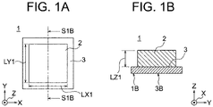
- Figs. 1A and 1B are a schematic plan view and a schematic cross-sectional view showing the configuration of a semiconductor element unit 1 according to a first embodiment.
- the semiconductor element unit 1 according to the first embodiment includes a semiconductor element 2 formed in a shape like a rectangular prism and a first electrode 3 formed in a shape like a thin plate.
- a direction heading from the left to the right in Fig. 1A will be represented as a +X direction
- a direction heading from the bottom to the top in Fig. 1A will be represented as a +Y direction
- a direction heading from the back to the front of the sheet of Fig. 1A will be represented as a +Z direction.
- Fig. 1B shows a cross section of the semiconductor element unit 1 of Fig. 1A sliced along the line S1B - S1B.
- the semiconductor element 2 is, for example, a light-emitting element including a cladding layer of the p-type or the n-type and an active layer.
- a surface facing the +Z direction i.e., upper surface in Fig. 1B
- a surface facing the -Z direction i.e., lower surface in Fig. 1B
- the shorter one of a length LX1 in the X direction and a length LY1 in the Y direction is less than or equal to 200 [ ⁇ m]
- a length (thickness) LZ1 in the Z direction is less than or equal to 20 [ ⁇ m], for example.
- the first electrode 3 is made of a metallic material having electrical conductivity such as Ti, Pt or Au, or alloy of such materials, for example.
- a first electrode mounting surface 3B as a surface facing the -Z direction is formed extremely flat and its surface roughness (roughness) is less than or equal to 10 [nm] .
- the first electrode 3 is formed in a shape like a flat rectangular prism, in which a length in the X direction and a length in the Y direction are both longer and a length in the Z direction is shorter compared to those of the semiconductor element 2.
- a surface of the semiconductor element 2 facing the -Z direction and a surface of the first electrode 3 facing the +Z direction are joined to each other and eutectic bonding is formed at their joining part.
- ohmic connection is realized between the semiconductor element 2 and the first electrode 3 by the eutectic bonding and specific resistance between them is less than or equal to 1.0 ⁇ 10 -2 [ ⁇ cm 2 ], for example.
- a surface of the semiconductor element unit 1 facing the -Z direction that is, the first electrode mounting surface 3B of the first electrode 3, will be referred to also as a unit mounting surface 1B.
- Figs. 2A to 2D are schematic cross-sectional views showing a manufacturing process (1) of the semiconductor element unit 1.
- Figs. 3A to 3E are schematic cross-sectional views showing a manufacturing process (2) of the semiconductor element unit 1.
- the +Z direction will be referred to also as an upward direction and the -Z direction will be referred to also as a downward direction in this description.
- the semiconductor element unit 1 is manufactured stepwise by prescribed manufacturing equipment 100 by successively executing former-stage steps for forming the semiconductor element 2 and latter-stage steps for combining the semiconductor element 2 and the first electrode 3 together.
- the manufacturing equipment 100 forms the semiconductor element 2 according to various manufacturing processes similar to those for manufacturing generic semiconductors. Specifically, as shown in Fig. 2A , the manufacturing equipment 100 executes a step of forming a growth sacrificial layer 32 on the upper side, namely, on the +Z direction side, of a prescribed growth substrate 31 and further forming a semiconductor functional layer 33 on the upper side of the growth sacrificial layer 32.
- the growth substrate 31 as the lowermost layer among these members is a silicon wafer, for example.
- An upper surface (surface facing the +Z direction) of the growth substrate 31 is formed extremely flat and its surface roughness is less than or equal to 10 [nm].
- the growth sacrificial layer 32 is a relatively thin layer made of Si (silicon), for example.
- Si silicon
- the semiconductor functional layer 33 is formed with the same material as the semiconductor element 2.
- the manufacturing equipment 100 executes a step of forming the semiconductor element 2 on the growth sacrificial layer 32 by removing unnecessary parts from the semiconductor functional layer 33.
- the manufacturing equipment 100 executes a step of sticking a stamp 101 on a surface of the semiconductor element 2 facing the +Z direction (upper surface) .
- the stamp 101 is a part of the manufacturing equipment 100 and is obtained by forming a material such as polydimethylsiloxane (PDMS) in a prescribed shape, for example.
- PDMS polydimethylsiloxane
- the manufacturing equipment 100 executes a step of removing the growth sacrificial layer 32 by means of an etching process using a solution of phosphoric acid or the like.
- the semiconductor element 2 reaches a state of having been stuck on the lower side of the stamp 101 and having been separated from the growth substrate 31.
- the manufacturing equipment 100 moves the stamp 101 to a prescribed storage area and thereby stores the semiconductor element 2 in the storage area together with the stamp 101.
- the manufacturing equipment 100 subsequently puts the semiconductor element 2 and the first electrode 3 in the combined state according to various manufacturing processes similar to those for manufacturing generic semiconductors. Specifically, first, as shown in Fig. 3A , the manufacturing equipment 100 executes a step of forming a formation sacrificial layer 42 on the upper side, i.e., on a surface facing the +Z direction, of a prescribed formation substrate 41.
- the formation substrate 41 is a silicon wafer, for example, similarly to the growth substrate 31 ( Figs. 2A to 2D ). Further, similarly to the case of the growth substrate 31, a surface of the formation substrate 41 facing the +Z direction (upper surface) is formed extremely flat and its surface roughness is less than or equal to 10 [nm] .
- the manufacturing equipment 100 may either use the previously used growth substrate 31 directly as the formation substrate 41 or use a formation substrate 41 different from the growth substrate 31.
- the formation sacrificial layer 42 is a relatively thin layer made of Al 2 O 3 (alumina), for example.
- a material that can be removed by wet etching performed in a subsequent step has been selected similarly to the case of the growth sacrificial layer 32.
- a surface of the formation sacrificial layer 42 facing the +Z direction is formed extremely flat and its surface roughness is less than or equal to 10 [nm].
- the manufacturing equipment 100 executes a step of forming the first electrode 3 like a thin film on the surface of the formation sacrificial layer 42 facing the +Z direction (upper surface).
- the first electrode 3 is formed with a metallic material such as Al or Ti, for example. Further, in the first electrode 3, the lengths in the X direction and the Y direction are both longer and the length in the Z direction (i.e., thickness) is shorter compared to those of the semiconductor element 2 manufactured in the former-stage steps.
- the first electrode mounting surface 3B as the surface of the first electrode 3 facing the -Z direction (lower surface) is formed extremely flat and its surface roughness is less than or equal to 10 [nm] due to influence of the surfaces of the formation substrate 41 and the formation sacrificial layer 42 facing the +Z direction (upper surfaces).
- the manufacturing equipment 100 executes a step of transferring the semiconductor element 2 manufactured in the former-stage steps onto the surface of the first electrode 3 facing the +Z direction (upper surface). Specifically, the manufacturing equipment 100 transfers the semiconductor element 2 onto the surface of the first electrode 3 facing the +Z direction (upper surface) by, for example, moving the stamp 101, on which the semiconductor element 2 has been stuck, from the prescribed storage area to a position in the +Z direction from (above) the first electrode 3 and moving the stamp 101 in the -Z direction (downward), that is, lowering the stamp 101. Thereafter, the manufacturing equipment 100 moves the stamp 101 alone in the +Z direction (upward), that is, elevates the stamp 101 alone, and thereby separates the stamp 101 from the semiconductor element 2, and then returns the stamp 101 to the storage area.
- the manufacturing equipment 100 moves the stamp 101 alone in the +Z direction (upward), that is, elevates the stamp 101 alone, and thereby separates the stamp 101 from the semiconductor element 2, and then returns the stamp 101 to the storage area.
- the manufacturing equipment 100 executes a step of an annealing process by placing the first electrode 3 and the semiconductor element 2, in the state in which the semiconductor element 2 is in contact with the surface of the first electrode 3 facing the +Z direction (upper surface) and the first electrode mounting surface 3B is in contact with the upper surface of the formation sacrificial layer 42, in an environment at approximately 600 [°C], for example.
- the semiconductor element 2 and the first electrode 3 form the eutectic bonding in the part where they are joined to each other, and consequently, the semiconductor element unit 1 is completed.
- the first electrode mounting surface 3B is in the state of being in contact with the upper surface of the formation sacrificial layer 42, and thus does not become rough even after the annealing process and maintains the extremely flat state.
- the formation substrate 41 and the formation sacrificial layer 42 in the state in which the completed semiconductor element unit 1 has been set on the formation sacrificial layer 42 will hereinafter be referred to as a supply substrate 40 or a semiconductor element unit supply substrate.
- the formation substrate 41 and the formation sacrificial layer 42 will also be referred to simply as a substrate, and the surface of the substrate, that is, the surface of the formation sacrificial layer 42 facing the +Z direction, will be referred to also as a substrate surface.
- the supply substrate 40 has a configuration with which the semiconductor element unit 1 can be conveyed stably in cases like when the manufacturer of the semiconductor element unit 1 and the other manufacturer that mounts the semiconductor element unit 1 on a prescribed circuit board are different from each other and the semiconductor element unit 1 has to be supplied from the manufacturer to the other manufacturer, for example.
- Figs. 4A and 4B are a schematic plan view and a schematic cross-sectional view showing the configuration of the supply substrate 40.
- Figs. 2A to 2D and Figs. 3A to 3E showed the state in which the manufacturing equipment 100 manufactures one semiconductor element unit 1, that is, the state in which one semiconductor element unit 1 is included in the supply substrate 40, for convenience of the explanation. However, as shown in Figs.
- the actual manufacturing equipment 100 is capable of manufacturing a plurality of semiconductor element units 1 in a lump in a state in which a plurality of semiconductor element units 1 are arranged in a grid on the formation substrate 41 and the formation sacrificial layer 42, that is, in a state in which a plurality of semiconductor element units 1 are included in one supply substrate 40.
- the semiconductor element units 1 are successively moved from the positions on the formation substrate 41 and the formation sacrificial layer 42 when manufacturing a semiconductor packaging circuit which will be described later. Specifically, first, as shown in Fig. 3D , the manufacturing equipment 100 executes a step of moving the stamp 101 and sticking the surface of the semiconductor element 2 of the semiconductor element unit 1 facing the +Z direction (upper surface) on the lower surface of the stamp 101.
- the manufacturing equipment 100 executes a step of removing the formation sacrificial layer 42 by means of an etching process using a solution of phosphoric acid or the like.
- the semiconductor element unit 1 reaches a state of having been stuck on the lower side of the stamp 101 and having been separated from the formation substrate 41.
- the manufacturing equipment 100 is capable of moving, i.e., supplying, the semiconductor element unit 1 to a desired position by moving the stamp 101.
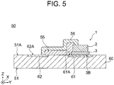
- Fig. 5 is a schematic cross-sectional view showing the configuration of the semiconductor packaging circuit 50 according to the first embodiment.
- the semiconductor packaging circuit 50 has a configuration in which the semiconductor element unit 1 is mounted on a circuit board 51 and is further provided with a first insulation part 55 and a wiring part 56.
- the circuit board 51 includes a base member part 60, a first circuit connection pad 61 and a second circuit connection pad 62, prescribed internal wiring members and drive circuit (not shown), and so forth.
- the base member part 60 is formed with the so-called glass epoxy resin, that is, formed by impregnating glass fiber with epoxy resin and thermally hardening the impregnated glass fiber, for example, and has sufficient strength, insulation performance, etc.
- the first circuit connection pad 61 is made of a material having electrical conductivity and exposes Al, for example, to its surface facing the +Z direction (hereinafter referred to as a "first pad surface 61A").
- the first circuit connection pad 61 exposes the first pad surface 61A to a surface of the circuit board 51 facing the +Z direction (hereinafter referred to as a "substrate surface 51A"), and is electrically connected to the prescribed wiring members (not shown) inside the circuit board 51.
- the lengths of the first circuit connection pad 61 in the X direction and the Y direction are respectively longer than the lengths of the first electrode 3 of the semiconductor element unit 1 ( Figs. 1A and 1B ) in the X direction and the Y direction.
- the second circuit connection pad 62 is configured similarly to the first circuit connection pad 61 and exposes its surface facing the +Z direction (hereinafter referred to as a "second pad surface 62A") to the substrate surface 51A.
- the substrate surface 51A is formed in an extremely flat planar shape. Namely, on the circuit board 51, the surface of the base member part 60, the first pad surface 61A and the second pad surface 62A are all extremely flat, are planes parallel to each other, and the distance between each other in regard to the Z direction (i.e., level difference) is also extremely small.
- the surface roughness of the substrate surface 51A namely, the surface roughness (roughness) at the base member part 60, the first pad surface 61A and the second pad surface 62A, is less than or equal to 10 [nm].
- the distances between the surface of the base member part 60 and the first pad surface 61A and between the surface of the base member part 60 and the second pad surface 62A in regard to the Z direction are less than or equal to 1/1000 in comparison with the shorter one of the length LX1 of the side in the X direction and the length LY1 of the side in the Y direction in the semiconductor element unit 1 ( Fig. 1A ).
- the semiconductor element unit 1 On the substrate surface 51A of the circuit board 51, the semiconductor element unit 1 has been set on the +Z direction side of the first pad surface 61A.
- the semiconductor element unit 1 is arranged to fit in the range of the first circuit connection pad 61 as viewed from a position on the +Z direction side of the semiconductor element unit 1, with the first electrode mounting surface 3B facing and in contact with the first pad surface 61A.
- the first insulation part 55 is a thin film formed with an organic material such as polyimide or an inorganic material such as a silicon nitride film, for example, and having insulation performance.
- the first insulation part 55 is provided so as to cover a range in regard to the Y direction from the vicinity of a - Y direction end of the surface of the semiconductor element 2 facing the +Z direction (i.e., upper surface) to the vicinity of a Y direction end of the second pad surface 62A.
- the wiring part 56 is formed with a material having electrical conductivity such as a metal like Au, Al, Cu, Ti or Pt or a compound like ITO (Indium Tin Oxide), for example.
- the wiring part 56 is provided to be overlaid on the +Z direction side (i.e., upper side) of the first insulation part 55, is in contact with the surface of the semiconductor element 2 facing the +Z direction (i.e., upper surface) and the second pad surface 62A, and electrically connects them to each other.
- the semiconductor packaging circuit 50 electrically connects a cathode on the -Z direction side (i.e., lower side) of the semiconductor element 2 of the semiconductor element unit 1 to the first circuit connection pad 61 while also electrically connecting an anode on the +Z direction side (i.e., upper side) of the semiconductor element 2 to the second circuit connection pad 62.
- the semiconductor packaging circuit 50 is capable of making the semiconductor element 2 as a light-emitting element emit light by applying and supplying prescribed voltage and prescribed current supplied from a non-illustrated drive circuit to the first circuit connection pad 61 and the second circuit connection pad 62.
- Figs. 6A to 6D are schematic cross-sectional views showing a manufacturing process of the semiconductor packaging circuit.
- Figs. 6A to 6D schematically show states in which the +Z direction is pointed in the upward direction similarly to Figs. 2A to 2D and Figs. 3A to 3E .
- the +Z direction will be referred to also as the upward direction and the -Z direction will be referred to also as the downward direction.
- the semiconductor packaging circuit 50 is manufactured stepwise by manufacturing equipment 100 according to various manufacturing processes similar to those for manufacturing generic semiconductors.
- the manufacturing equipment 100 that manufactures the semiconductor packaging circuit 50 may be either the same as or different from the manufacturing equipment 100 that manufactured the semiconductor element unit 1.
- the manufacturing equipment 100 manufactures the circuit board 51 to a state in which the first pad surface 61A and the second pad surface 62A are exposed to the surface of the base member part 60.
- the manufacturing equipment 100 is capable of manufacturing the circuit board 51 in a state in which the substrate surface 51A is extremely flat, that is, the base member part 60, the first pad surface 61A and the second pad surface 62A are all extremely flat and the level differences between each other are extremely small, by executing processing like chemical mechanical polishing, for example.
- the manufacturing equipment 100 executes a step of transferring the semiconductor element unit 1 onto the first circuit connection pad 61 of the circuit board 51. Specifically, the manufacturing equipment 100 moves the stamp 101 on which the semiconductor element unit 1 has been stuck ( Fig. 3E ) to a position in the +Z direction from (i.e., above) the first circuit connection pad 61 of the circuit board 51, and further moves the stamp 101 in the -Z direction (i.e., downward), that is, lowers the stamp 101. By this step, the semiconductor element unit 1 reaches a state in which the first electrode mounting surface 3B is facing and in contact with the first pad surface 61A.
- the manufacturing equipment 100 executes a step of forming the first insulation part 55 in a range on the circuit board 51 extending from a part of the surface of the semiconductor element 2 facing the +Z direction (upper surface) to a part of the second pad surface 62A.
- the manufacturing equipment 100 executes a step of forming the wiring part 56 on the circuit board 51 so as to overlay the wiring part 56 on the +Z direction side (upper side) of the first insulation part 55. Accordingly, the wiring part 56 electrically connects the semiconductor element 2 and the second circuit connection pad 62.
- the manufacturing equipment 100 is capable of manufacturing the semiconductor packaging circuit 50 ( Fig. 5 ) as described above.
- Fig. 7 is a schematic perspective view showing the configuration of an LED display device 70.
- a plurality of semiconductor element units 1 have been installed in the LED display device 70 shown in Fig. 7 .
- a plurality of semiconductor packaging circuits 50 have been installed in the LED display device 70.
- the LED display device 70 includes an LED display type display unit 71, a frame 72, a heat radiation member 73, a connection cable 74, a connection terminal unit 75, a display driver 76, and so forth.
- the LED display device 70 which is referred to also as a micro-LED display, is a display in which a set of LED elements of red, green and blue is provided corresponding to one pixel.
- the LED display type display unit 71 has a configuration in which a plurality of semiconductor element units 1 ( Fig. 1A ) are installed to be arranged like a grid in a display region that is set on a surface of a planar display circuit board 71D facing the +Z direction.
- the display circuit board 71D is, for example, a so-called glass epoxy substrate similar to the circuit board 51, and has a configuration like a plurality of circuit boards 51 arrayed in a grid.
- the frame 72 is formed in a shape like a rectangular frame with a prescribed steel material or the like, for example, and is attached to the LED display type display unit 71 to surround the outer periphery of the display region on the +Z direction side of the LED display type display unit 71.
- the heat radiation member 73 is formed in a shape like a flat rectangular prism as a whole with a metallic material having relatively high thermal conductivity like aluminum, for example.
- the heat radiation member 73 is set to be in contact with the LED display type display unit 71 on the -Z direction side of the LED display type display unit 71, that is, on a side opposite to the surface for displaying images and the like.
- the connection cable 74 is electrically connected to a prescribed control device (not shown) via the connection terminal unit 75 and thereby transmits and supplies an image signal, supplied from the control device, to the display driver 76.
- the display driver 76 as a drive circuit is electrically connected to the connection cable 74 and the LED display type display unit 71.
- the display driver 76 generates drive signals of red, green and blue based on the image signal supplied via the connection cable 74 and supplies drive currents based on these drive signals to the LED display type display unit 71. Consequently, the LED display device 70 is capable of displaying an image based on the image signal supplied from the control device (not shown) or the like in the display region of the LED display type display unit 71.
- the semiconductor element unit 1 according to the first embodiment is formed so that the surface of the semiconductor element 2 facing the -Z direction and the surface of the first electrode 3 facing the +Z direction are connected to each other by eutectic bonding and the first electrode mounting surface 3B as the surface of the first electrode 3 facing the -Z direction is maintained in the extremely flat state ( Figs. 1A and 2B ).
- the manufacturing equipment 100 manufacturing the semiconductor element unit 1 forms the first electrode 3 like a thin film on the +Z direction side (upper side) of the formation sacrificial layer 42 ( Fig. 3B ) in the state of having been formed on the formation substrate 41, transfers the semiconductor element 2 manufactured separately ( Figs. 2A to 2D ) onto the first electrode 3 ( Fig. 3C ), and executes the annealing process in this state.
- the manufacturing equipment 100 executes the annealing process while leaving the first electrode mounting surface 3B in the state of being in contact with the formation sacrificial layer 42, by which the first electrode 3 and the semiconductor element 2 can be connected to each other by eutectic bonding while maintaining the extremely flat state of the first electrode mounting surface 3B without roughening the first electrode mounting surface 3B.
- the substrate surface 51A of the circuit board 51 is formed extremely flat and the level differences relative to the first pad surface 61A and the second pad surface 62A are also held down to be extremely small ( Fig. 5 ).
- the manufacturing equipment 100 when manufacturing the semiconductor packaging circuit 50 by mounting the semiconductor element unit 1 on the circuit board 51, the manufacturing equipment 100 is capable of making intermolecular force act between the first electrode mounting surface 3B and the first pad surface 61A just by transferring the semiconductor element unit 1 so as to make the first electrode mounting surface 3B contact the first pad surface 61A.
- the first electrode 3 of the semiconductor element unit 1 can be physically and electrically connected to the first circuit connection pad 61 of the circuit board 51.
- the semiconductor element 2 can be electrically connected excellently to the drive circuit (not shown) of the circuit board 51 just by making the first electrode mounting surface 3B contact the first pad surface 61A of the circuit board 51.
- the semiconductor element unit 1 the semiconductor element 2 and the drive circuit can be electrically connected excellently to each other without the need of executing the annealing process after the mounting on the circuit board 51, and thus damage caused to the drive circuit due to heat of the annealing process can be avoided in principle.
- the semiconductor element 2 and the first electrode 3 are connected to each other by eutectic bonding and the first electrode mounting surface 3B is maintained in the extremely flat state by executing the annealing process in the state in which the overlaid first electrode 3 and semiconductor element 2 have been set on the formation sacrificial layer 42.
- the semiconductor element unit 1 when the semiconductor element unit 1 is mounted on the circuit board 51 whose substrate surface 51A has been formed extremely flat, it is possible to make intermolecular force act between the first electrode mounting surface 3B and the first pad surface 61A and thereby physically and electrically connect them with each other just by transferring the semiconductor element unit 1 so as to make the first electrode mounting surface 3B contact the first pad surface 61A, and it is unnecessary to execute the annealing process after the mounting.
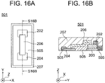
- Figs. 8A and 8B are a schematic plan view and a schematic cross-sectional view showing the configuration of a semiconductor element unit 201 according to a second embodiment.
- the semiconductor element unit 201 according to the second embodiment is formed with a semiconductor element 202, a first electrode 203, a second electrode 204, a first insulation part 205, a wiring part 206 and a second insulation part 207.
- the semiconductor element unit 201 has a configuration similar to a part of the semiconductor packaging circuit 50 in the first embodiment ( Fig. 5 ) that is provided on the circuit board 51.
- the semiconductor element 202 is configured similarly to the semiconductor element 2 according to the first embodiment. Namely, the semiconductor element 202 is in a shape like a rectangular prism and is formed as a light-emitting element, for example.
- the first electrode 203 is configured similarly to the first electrode 3 according to the first embodiment, formed in a shape like a flat rectangular prism as a whole, and made of a metallic material having electrical conductivity or alloy of such materials. Further, similarly to the first embodiment, the first electrode 203 is in contact with the -Z direction side of the semiconductor element 202 and eutectic bonding is formed at their joining part. Furthermore, similarly to the first electrode mounting surface 3B according to the first embodiment, a first electrode mounting surface 203B as a surface of the first electrode 203 facing the -Z direction is formed extremely flat and its surface roughness is less than or equal to 10 [nm].
- the second electrode 204 is formed in a shape like a flat rectangular prism as a whole and made of a metallic material having electrical conductivity such as Au, Al, Cu, Ti or Pt, or alloy of such materials, for example.
- a second electrode mounting surface 204B as a surface of the second electrode 204 facing the -Z direction is formed extremely flat and its surface roughness is less than or equal to 10 [nm].
- the first insulation part 205 is a thin film formed with an organic material such as polyimide or an inorganic material such as a silicon nitride film, for example, and having insulation performance.
- the first insulation part 205 is provided so as to cover a range in regard to the Y direction from the vicinity of a -Y direction end of a surface of the semiconductor element 202 facing the +Z direction (i.e., upper surface) to the vicinity of a Y direction end of a surface of the second electrode 204 facing the +Z direction (i.e., upper surface).
- the wiring part 206 is formed with a material having electrical conductivity such as a metal like Au, Al, Cu, Ti or Pt or a compound like ITO (Indium Tin Oxide), for example.
- This wiring member is provided to be overlaid on the +Z direction side (i.e., upper side) of the first insulation part 205, is in contact with the surface of the semiconductor element 202 facing the +Z direction (i.e., upper surface) and the surface of the second electrode 204 facing the +Z direction (i.e., upper surface), and electrically connects them to each other.
- the second insulation part 207 is a thin film formed with an organic material such as polyimide or an inorganic material such as a silicon nitride film, for example, and having insulation performance.
- the second insulation part 207 is provided in a wide range to cover the semiconductor element 202, the first electrode 203, the second electrode 204, the first insulation part 205 and the wiring part 206 from the +Z direction side and to surround them in regard to the X direction and the Y direction.
- the second insulation part 207 covers the semiconductor element 202, the first electrode 203, the second electrode 204, the first insulation part 205 and the wiring part 206 from any direction except for the -Z direction side (i.e., lower side).
- the surface of the second electrode 204 facing the -Z direction will be referred to as the second electrode mounting surface 204B
- a surface of the first insulation part 205 facing the -Z direction will be referred to as a first insulation part mounting surface 205B
- a surface of the semiconductor element unit 201 facing the -Z direction that is, the first electrode mounting surface 203B, the second electrode mounting surface 204B, the first insulation part mounting surface 205B and a surface of the second insulation part 207 facing the -Z direction put together, will be referred to also as a unit mounting surface 201B.
- the unit mounting surface 201B is formed extremely flat as a whole and its surface roughness is less than or equal to 10 [nm].
- the first insulation part 205 has a first insulation part mounting surface 205B situated on the unit mounting surface
- the second insulation part 207 has a second insulation part mounting surface 207B situated on the unit mounting surface.
- the size of the level difference (i.e., length in the Z direction) at each part where different materials adjoin each other on the unit mounting surface 201B, e.g., a part where the first electrode 203 adjoins the first insulation part 205, is at a value sufficiently smaller in comparison with each side forming the external form of the unit mounting surface 201B.
- the size of the level difference is less than or equal to 1/1000 of a length (LX in the example of Fig. 8A ) as the shorter one of the length LX of a side of the semiconductor element unit 201 in the X direction and the length LY of a side of the semiconductor element unit 201 in the Y direction.
- a size of a level difference of the unit mounting surface 201B at a part where different materials adjoin each other is less than or equal to 1/1000 of a length of a shortest side in an external form of a surface of the second insulation part 207 parallel to the unit mounting surface 201B.
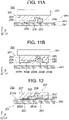
- Figs. 9A to 9D Figs. 10A to 10G and Figs. 11A and 11B are schematic cross-sectional views showing manufacturing processes (1) to (3) of the semiconductor element unit according to the second embodiment.
- Figs. 9A to 9D Figs. 10A to 10G and Figs. 11A and 11B are schematic side views or cross-sectional views showing states in which the +Z direction is pointed in the upward direction in the same way as in the first embodiment.
- the +Z direction will be referred to also as the upward direction and the -Z direction will be referred to also as the downward direction in this description.
- the semiconductor element unit 201 is manufactured stepwise by prescribed manufacturing equipment 100 by successively executing former-stage steps for forming the semiconductor element 202 and latter-stage steps for combining the semiconductor element 202 with the first electrode 203 and the like.
- the manufacturing equipment 100 forms the semiconductor element 202 according to various manufacturing processes similar to those for manufacturing generic semiconductors similarly to the first embodiment. Specifically, as shown in Fig. 9A corresponding to Fig. 2A , the manufacturing equipment 100 executes a step of forming a growth sacrificial layer 232 on the upper side, namely, on the +Z direction side, of a prescribed growth substrate 231 and further forming a semiconductor functional layer 233 on the upper side of the growth sacrificial layer 232.
- the growth substrate 231, the growth sacrificial layer 232 and the semiconductor functional layer 233 are respectively configured similarly to the growth substrate 31, the growth sacrificial layer 32 and the semiconductor functional layer 33 in the first embodiment.
- the manufacturing equipment 100 puts the semiconductor element 202 in a state of having been stuck on the lower side of the stamp 101 by successively executing steps of the removal of unnecessary parts, the etching process, etc.
- the manufacturing equipment 100 subsequently puts the semiconductor element 202 and the first electrode 203 and the like in the combined state according to various manufacturing processes similar to those for manufacturing generic semiconductors.
- the manufacturing equipment 100 executes a step of forming a formation sacrificial layer 242 on the upper side, i.e., the +Z direction side, of a prescribed formation substrate 241.
- the formation substrate 241 and the formation sacrificial layer 242 are configured similarly to the formation substrate 41 and the formation sacrificial layer 42 in the first embodiment. Namely, a surface of the formation sacrificial layer 242 facing the +Z direction (upper surface) is formed extremely flat and its surface roughness is less than or equal to 10 [nm].
- the manufacturing equipment 100 executes a step of forming the first electrode 203 like a thin film on the +Z direction side (upper side) of the formation sacrificial layer 242.
- the first electrode 203 is formed with a metallic material such as Ti or Pt, for example.
- the first electrode mounting surface 203B is formed extremely flat and its surface roughness is less than or equal to 10 [nm] due to the influence of the surfaces of the formation sacrificial layer 242 facing the +Z direction (upper surface).
- the manufacturing equipment 100 executes a step of forming the second electrode 204 like a thin film on the surfaces of the formation sacrificial layer 242 facing the +Z direction (upper surface).
- the second electrode 204 is formed with an alloy material such as AuGeNi, for example.
- the second electrode mounting surface 204B is formed extremely flat and its surface roughness is less than or equal to 10 [nm] due to the influence of the surfaces of the formation sacrificial layer 242 facing the +Z direction (upper surface).
- the manufacturing equipment 100 executes a step of transferring the semiconductor element 202 manufactured in the former-stage steps onto the surface of the first electrode 203 facing the +Z direction (upper surface). Specifically, the manufacturing equipment 100 transfers the semiconductor element 202 onto the +Z direction side (upper side) of the first electrode 203 by, for example, moving the stamp 101 ( Fig. 9D ), on which the semiconductor element 202 has been stuck, to a position on the +Z direction side (upper side) of the first electrode 203 and moving the stamp 101 towards the -Z direction side (lower side).
- the manufacturing equipment 100 executes a step of the annealing process by placing the first electrode 203 and the semiconductor element 202, in the state in which the semiconductor element 202 is in contact with the +Z direction side (upper side) of the first electrode 203 and the first electrode mounting surface 203B and the second electrode mounting surface 204B are in contact with the upper surface of the formation sacrificial layer 242, in an environment at approximately 600 [°C], for example.
- the semiconductor element 202 and the first electrode 203 form the eutectic bonding in the part where they are joined to each other.
- the first electrode mounting surface 203B and the second electrode mounting surface 204B are both in the state of being in contact with the upper surface of the formation sacrificial layer 242, and thus do not become rough even after the annealing process and maintain the extremely flat state.
- the manufacturing equipment 100 executes a step of forming the first insulation part 205 in a range on the formation sacrificial layer 242 extending from a part of the surface of the semiconductor element 202 facing the +Z direction (upper surface) to a part of the surface of the second electrode 204 facing the +Z direction (upper surface).
- the manufacturing equipment 100 executes a step of forming the wiring part 206 over the circuit board 51 so as to overlay the wiring part 206 on the +Z direction side (upper side) of the first insulation part 205. Accordingly, the wiring part 206 electrically connects the surface of the semiconductor element 202 facing the +Z direction (upper surface) and the surface of the second electrode 204 facing the +Z direction (upper surface).
- the manufacturing equipment 100 executes a step of forming the second insulation part 207 on the formation sacrificial layer 242 so as to overlay the second insulation part 207 on the +Z direction side (upper side) of the semiconductor element 202, the first insulation part 205, the wiring part 206, etc. Accordingly, the second insulation part 207 covers the +Z direction side, the +X direction side, the -X direction side, the +Y direction side and the -Y direction side of the structure formed with the semiconductor element 202, the first electrode 203, the second electrode 204, the first insulation part 205 and the wiring part 206.
- the second insulation part 207 covers all of top surfaces and side faces of the structure formed with the semiconductor element 202, the first electrode 203, the second electrode 204, the first insulation part 205 and the wiring part 206. Consequently, the manufacturing equipment 100 can complete the semiconductor element unit 201.
- the formation substrate 241 and the formation sacrificial layer 242 in the state in which the completed semiconductor element unit 201 has been set on the formation sacrificial layer 242 will be referred to as a supply substrate 240 or a semiconductor element unit supply substrate.
- the formation substrate 241 and the formation sacrificial layer 242 will also be referred to simply as a substrate, and the surface of the substrate, that is, the surface of the formation sacrificial layer 242 facing the +Z direction, will be referred to also as a substrate surface.
- the actual manufacturing equipment 100 is capable of manufacturing a plurality of semiconductor element units 201 in a lump in a state in which a plurality of semiconductor element units 201 are arranged on the formation substrate 241 and the formation sacrificial layer 242, that is, in a state in which a plurality of semiconductor element units 201 are included in one supply substrate 240.
- manufacturing equipment 100 executes a step of sticking the surface of the second insulation part 207 of the semiconductor element unit 201 facing the +Z direction (upper surface) on the lower surface of the stamp 101.
- the manufacturing equipment 100 that executes this step may be either the same as or different from the manufacturing equipment 100 that manufactured the semiconductor element unit 201.
- the manufacturing equipment 100 executes a step of removing the formation sacrificial layer 242 by means of an etching process using a solution of phosphoric acid or the like.
- the manufacturing equipment 100 puts the semiconductor element unit 201 in a state of having been stuck on the lower side of the stamp 101 and having been separated from the formation substrate 241.
- the manufacturing equipment 100 is capable of moving, i.e., supplying, the semiconductor element unit 201 to a desired position by moving the stamp 101.
- Fig. 12 is a schematic cross-sectional view showing the configuration of the semiconductor packaging circuit 250 according to the second embodiment.
- the semiconductor packaging circuit 250 has a configuration in which the semiconductor element unit 201 is mounted on a circuit board 251.
- the circuit board 251 is configured similarly to the circuit board 51 according to the first embodiment ( Fig. 5 ) and includes a base member part 260, a first circuit connection pad 261 and a second circuit connection pad 262 respectively corresponding to the base member part 60, the first circuit connection pad 61 and the second circuit connection pad 62.
- surfaces of the first circuit connection pad 261 and the second circuit connection pad 262 facing the +Z direction will be referred to as a first pad surface 261A and a second pad surface 262A, respectively.
- a substrate surface 251A as the surface facing the +Z direction is formed in an extremely flat planar shape similarly to the first embodiment. Namely, on the circuit board 251, the surface of the base member part 260, the first pad surface 261A and the second pad surface 262A are all extremely flat, are planes parallel to each other, and the distance between each other in regard to the Z direction (i.e., level difference) is also extremely small.
- the semiconductor packaging circuit 250 is manufactured by manufacturing equipment 100 according to various manufacturing processes similar to those for manufacturing generic semiconductors, for example.
- the manufacturing equipment 100 that manufactures the semiconductor packaging circuit 250 may be either the same as or different from the manufacturing equipment 100 that manufactured the semiconductor element unit 201.
- the manufacturing equipment 100 manufactures the circuit board 251 to a state in which the first pad surface 261A and the second pad surface 262A are exposed to the surface of the base member part 260.
- the manufacturing equipment 100 brings the circuit board 251 to a state in which the substrate surface 251A is extremely flat by executing processing like chemical mechanical polishing, for example, similarly to the first embodiment.
- the surface roughness of the substrate surface 251A namely, the surface roughness (roughness) at the base member part 260, the first pad surface 261A and the second pad surface 262A, is less than or equal to 10 [nm] similarly to the first embodiment.
- the distances in regard to the Z direction i.e., level difference heights
- this level difference height i.e., permissible level difference height
- this level difference height is less than or equal to 1/1000 in comparison with the shorter one of the length LX of the side in the X direction and the length LY of the side in the Y direction in the semiconductor element unit 201 ( Fig. 8A ).
- the manufacturing equipment 100 executes a step of transferring the semiconductor element unit 201 stuck on the stamp 101 onto the substrate surface 251A of the circuit board 251.
- the manufacturing equipment 100 moves the stamp 101, on which one semiconductor element unit 201 has been stuck, to a position on the +Z direction side of a part of the circuit board 251 on which no other semiconductor element unit 201 has been stuck yet. At that time, the manufacturing equipment 100 executes positioning of the stamp 101 in regard to the X direction and the Y direction so that the whole range of the first electrode 203 of the semiconductor element unit 201 faces the first pad surface 261A and the whole range of the second electrode 204 faces the second pad surface 262A.
- the manufacturing equipment 100 moves the stamp 101 in the -Z direction (i.e., downward) and thereby makes the unit mounting surface 201B of the semiconductor element unit 201 contact the substrate surface 251A of the circuit board 251.
- the semiconductor element unit 201 has its first electrode mounting surface 203B contact the first pad surface 261A, has its second electrode mounting surface 204B contact the second pad surface 262A, and has its first insulation part mounting surface 205B and second insulation part mounting surface 207B contact the surface of the base member part 260.
- the manufacturing equipment 100 makes the stamp 101 apply prescribed pressure in the -Z direction (i.e., downward direction) to (press against) the semiconductor element unit 201.
- the intermolecular force is made to act between the unit mounting surface 201B and the substrate surface 251A and the semiconductor element unit 201 is stuck on the circuit board 251 by the intermolecular force.
- the first electrode mounting surface 203B is electrically connected to the first pad surface 261A by the bonding by the intermolecular force.
- the second electrode mounting surface 204B is electrically connected to the second pad surface 262A by the bonding by the intermolecular force.
- the first electrode 203 and the second electrode 204 are electrically connected respectively to the first circuit connection pad 261 and the second circuit connection pad 262. Accordingly, in the semiconductor packaging circuit 250, it is possible to supply electric current from a drive circuit (not shown) of the circuit board 251 to the semiconductor element 202 of the semiconductor element unit 201 and thereby make the semiconductor element 202 emit light.
- the semiconductor element unit 201 is bonded to the circuit board 251 by the intermolecular force, applying force stronger than the intermolecular force can cancel the bonding and easily peel off the semiconductor element unit 201 from the circuit board 251.
- the manufacturing equipment 100 makes a non-illustrated peeling head approach the semiconductor packaging circuit 250 and discharge a prescribed solvent and thereby lowers the bonding force of the semiconductor element unit 201. Subsequently, the manufacturing equipment 100 can peel off and remove the semiconductor element unit 201 from the circuit board 251 by moving the stamp 101 to the semiconductor element unit 201, making the stamp 101 suck the semiconductor element unit 201, and moving the stamp 101. At that time, the circuit board 251 is hardly damaged, and when another semiconductor element unit 201 is subsequently transferred thereto, the circuit board 251 is capable of bonding to the semiconductor element unit 201 by the intermolecular force.
- the semiconductor packaging circuit 250 is manufactured as a part of the LED display device 70 ( Fig. 7 ), for example.
- the display circuit board 71D as a part of the LED display type display unit 71 has a configuration like a plurality of circuit boards 251 arrayed in a grid, for example.
- the first circuit connection pad 261 and the second circuit connection pad 262 have been provided in each part corresponding to each circuit board 251, and each mounting part as a part on which each semiconductor element unit 201 should be mounted has been set.
- the manufacturing equipment 100 When manufacturing the LED display device 70, the manufacturing equipment 100 successively mounts a plurality of semiconductor element units 201 on the aforementioned display circuit board 71D.
- one semiconductor element unit 201 corresponds to one pixel.
- some millions of semiconductor element units 201 are mounted on the display circuit board 71D depending on the resolution of the display circuit board 71D.
- the semiconductor element unit 201 has a possibility of occurrence of a defective product due to a problem in the manufacture or the like. Then, when a part of the semiconductor element units 201 mounted on the LED display device 70 are defective products, for example, the LED display device 70 is necessitated to have a failure such as some pixels incapable of displaying normally, is judged to be defective in a test before shipment or the like, and can be discarded without being shipped.
- the manufacturing equipment 100 can test whether each semiconductor element unit 201 mounted on the display circuit board 71D operates normally or not and replace the semiconductor element unit 201 with a new semiconductor element unit 201 when the semiconductor element unit 201 is defective.
- Fig. 13 is a flowchart showing a manufacturing process of the semiconductor packaging circuit 250.
- the manufacturing equipment 100 executes the manufacturing process RT1 shown in Fig. 13 when mounting a plurality of semiconductor element units 201 on the display circuit board 71D.
- the manufacturing equipment 100 shifts to the first step SP1, makes the stamp 101 ( Figs. 11A and 11B ) successively transfer the semiconductor element units 201 onto the mounting parts on the display circuit board 71D, and shifts to the next step SP2.
- This brings the display circuit board 71D to a state in which the semiconductor element units 201 are bonded to the mounting parts by the intermolecular force and the display circuit board 71D is connected to the semiconductor element units 201 also electrically.
- the manufacturing equipment 100 makes the semiconductor element units 201 at the mounting parts respectively emit light by supplying a prescribed signal to a drive circuit provided on the display circuit board 71D, and shifts to the next step SP3.
- the manufacturing equipment 100 makes a prescribed image capturing unit capture an image of light emission conditions of the semiconductor element units 201 at the mounting parts and generates a test image by performing prescribed image processing on the captured image, and shifts to the next step SP4.
- the manufacturing equipment 100 divides the display circuit board 71D into a plurality of regions and generates the test image in regard to each of the regions.
- the manufacturing equipment 100 judges based on the test image whether each mounting part is a normal part where the mounted semiconductor element unit 201 is emitting light normally or an abnormal part where the mounted semiconductor element unit 201 is not emitting light normally, and shifts to the next step SP5. In short, the manufacturing equipment 100 checks the light emission condition of each semiconductor element unit 201 mounted on the display circuit board 71D by using the test image.
- the manufacturing equipment 100 judges whether or not there is at least one abnormal part on the display circuit board 71D.
- an affirmative result is obtained in the judgment, it means that a normal LED display device 70 cannot be manufactured by using the display circuit board 71D since at least one of the plurality of semiconductor element units 201 mounted on the display circuit board 71D is not emitting light normally.
- the mounting part can be changed to a normal part if the semiconductor element unit 201 at the mounting part as the abnormal part is replaced and the semiconductor element unit 201 after the replacement emits light normally. Accordingly, the manufacturing equipment 100 shifts to the next step SP6.
- the manufacturing equipment 100 makes the non-illustrated peeling head discharge a prescribed solvent towards the abnormal part and thereby lowers the bonding force of the semiconductor element unit 201 at the abnormal part, removes the semiconductor element unit 201 from the abnormal part by using the stamp 101, and shifts to the next step SP7.
- the manufacturing equipment 100 removes all of the semiconductor element units 201 at the abnormal parts.
- the manufacturing equipment 100 makes the stamp 101 transfer a new semiconductor element unit 201 onto the abnormal part and thereby has the new semiconductor element unit 201 bonded to the display circuit board 71D by the intermolecular force. Thereafter, the manufacturing equipment 100 judges whether the mounting part that was abnormal has changed to operate normally or not by returning to the step SP2 and repeating the series of processes.
- step SP5 when a negative result is obtained in the step SP5, it means that the mounted semiconductor element units 201 are operating normally at all of the mounting parts on the display circuit board 71D, that is, the LED display type display unit 71 with all the pixels operating normally is completed. In this case, the manufacturing equipment 100 shifts to the next step SP8 and ends the manufacturing process RT1.
- the semiconductor element unit 201 is formed so that the surface of the semiconductor element 202 facing the -Z direction and the surface of the first electrode 203 facing the +Z direction are connected to each other by eutectic bonding, the semiconductor element 202 and the second electrode 204 are connected to each other by the wiring part 206, and the unit mounting surface 201B is extremely flat ( Fig. 8B ).
- the manufacturing equipment 100 manufacturing the semiconductor element unit 201 forms the first electrode 203 and the second electrode 204 like thin films on the +Z direction side (upper side) of the formation sacrificial layer 242 ( Figs. 10B and 10C ) in the state of having been formed on the formation substrate 241. Subsequently, the manufacturing equipment 100 transfers the semiconductor element 202 manufactured separately ( Figs. 9A to 9D ) onto the +Z direction side of the first electrode 203 ( Fig. 10D ) and executes the annealing process in this state.
- the manufacturing equipment 100 executes the annealing process while leaving the first electrode mounting surface 203B and the second electrode mounting surface 204B in the state of being in contact with the formation sacrificial layer 242, by which the first electrode 203 and the semiconductor element 202 can be connected to each other by eutectic bonding while maintaining the extremely flat state of the first electrode mounting surface 203B and the second electrode mounting surface 204B without roughening the first electrode mounting surface 203B and the second electrode mounting surface 204B.
- the manufacturing equipment 100 forms the first insulation part 205 and the second insulation part 207 on the formation sacrificial layer 242 ( Figs. 10E and 10G ). Therefore, the manufacturing equipment 100 can form the first insulation part mounting surface 205B and the second insulation part mounting surface 207B extremely flat, hold down the level differences relative to the first electrode mounting surface 203B and the second electrode mounting surface 204B to be extremely small, and finish the whole of the unit mounting surface 201B of the semiconductor element unit 201 extremely flat.
- the semiconductor element unit 201 manufactured as above is transferred onto the circuit board 251 ( Fig. 12 ) so that the unit mounting surface 201B is in contact with the substrate surface 251A of the circuit board 251, the intermolecular force acts between the unit mounting surface 201B and the substrate surface 251A and the semiconductor element unit 201 can be bonded to the circuit board 251 with sufficient strength.
- the semiconductor element unit 201 is capable of having the first electrode 203 and the second electrode 204 electrically connected respectively to the first circuit connection pad 261 and the second circuit connection pad 262.
- the semiconductor element units 201 can be physically joined and electrically connected to the display circuit board 71D, that is, mounted on the display circuit board 71D, just by transferring the semiconductor element units 201 onto the plurality of mounting parts provided on the display circuit board 71D.
- the manufacturing equipment 100 can check whether or not each of the mounted semiconductor element units 201 emits light normally or not by supplying current thereto, and when there is an abnormal part not emitting light normally, the manufacturing equipment 100 can easily peel off and replace the semiconductor element unit 201 practically without damaging the display circuit board 71D. Consequently, the manufacturing equipment 100 can remarkably increase the ratio of non-defective products, namely, the so-called manufacturing yield, in regard to the LED display type display unit 71 and the LED display device 70.
- the semiconductor element 202 and the first electrode 203 are connected to each other by eutectic bonding and the unit mounting surface 201B including the first electrode mounting surface 203B and the second electrode mounting surface 204B is formed to be in the extremely flat state. Accordingly, in the manufacture of the semiconductor packaging circuit 250, just by transferring the semiconductor element unit 201 onto the circuit board 251, the unit mounting surface 201B and the substrate surface 251A can be bonded to each other by the intermolecular force, the test of the light emission condition can be executed in this state, and the replacement work at the abnormal part can be executed with ease.
- Figs. 14A and 14B are a schematic plan view and a schematic cross-sectional view showing the configuration of a semiconductor element unit 301 according to a third embodiment.
- the description is given of the case where only the first electrode 3 is joined to the semiconductor element 2 of the semiconductor element unit 1 ( Figs. 1A and 1B ).
- a direct top electrode 311 may be provided on the surface of the semiconductor element 2 facing the +Z direction, that is, the upper surface different from a joint surface joined to the first electrode 3.
- the manufacturing equipment 100 transfers the semiconductor element 2 onto the upper side of the first electrode 3 as shown in Fig.
- the semiconductor element unit 301 is capable of forming the eutectic bonding between the semiconductor element 2 and the first electrode 3 and between the semiconductor element 2 and the direct top electrode 311 as well. Further, in this case, the light emitted by the light emission by the semiconductor element 2 can be efficiently transmitted in the +Z direction by forming the direct top electrode 311 with a material having high light permeability as a so-called transparent electrode, for example,
- the description of the semiconductor packaging circuit 50 ( Fig. 5 ) is given of the case where the first circuit connection pad 61 is formed to be larger (longer) than the first electrode 3 in regard to the X direction and the Y direction and the first electrode mounting surface 3B is mounted at a position to face the inside of the range of the first pad surface 61A.
- the substrate surface 51A is desired to be as flat as possible.
- the size of the level difference namely, the distance in regard to the Z direction, between the surface of the base member part 60 facing the +Z direction and the first pad surface 61A is desired to be less than or equal to 1/1000 of the lengths of the semiconductor element unit 301 in the X direction and the Y direction.
- the level differences among the first electrode 203, the second electrode 204, the first insulation part 205 and the second insulation part 207 are also desired to be less than or equal to 1/1000 of the lengths of the semiconductor element unit 201 in the X direction and the Y direction.
- the semiconductor element unit 1 stuck on the lower surface of the stamp 101 as shown in Fig. 3E as the supply substrate or to use the semiconductor element unit 1 transferred from the stamp 101 onto a prescribed substrate as the supply substrate.
- the semiconductor element units 201 may be used instead of the semiconductor element units 1.
- semiconductor element units 1 i.e., those including a mixture of a plurality of types of semiconductor elements 2 stuck on the lower surface of the stamp 101 as the supply substrate, or to use semiconductor element units 1 transferred onto a prescribed substrate as the supply substrate.
- semiconductor element units 1 i.e., those including a mixture of a plurality of types of semiconductor elements 2 stuck on the lower surface of the stamp 101 as the supply substrate, or to use semiconductor element units 1 transferred onto a prescribed substrate as the supply substrate.
- a plurality of semiconductor element units 201 transferred onto a prescribed substrate may be used as the supply substrate.
- an LED display type display unit 71 capable of performing color display can be implemented by, for example, mounting red semiconductor element units 1 employing semiconductor elements 2 emitting red light, green semiconductor element units 1 employing semiconductor elements 2 emitting green light, and blue semiconductor element units 1 employing semiconductor elements 2 emitting blue light on the display circuit board 71D so that red, green and blue semiconductor element units 1 are arranged repeatedly. The same applies to the second embodiment.
- an LED display type display unit 71 capable of performing color display can be implemented by mounting red semiconductor element units 201, green semiconductor element units 201 and blue semiconductor element units 201 on the display circuit board 71D so that red, green and blue semiconductor element units 201 are arranged regularly.
- Figs. 15A and 15B are a schematic plan view and a schematic cross-sectional view showing the configuration of a semiconductor element unit 401 according to a fourth embodiment.
- the description is given of the case where only the first electrode 203 is joined to the semiconductor element 202 of the semiconductor element unit 201 ( Figs. 8A and 8B ) .
- a direct top electrode 411 may be provided on the surface of the semiconductor element 202 facing the +Z direction, that is, the upper surface on the side opposite to the surface joined to the first electrode 203.
- the manufacturing equipment 100 transfers the semiconductor element 202 onto the upper side of the first electrode 203 as shown in Fig. 10D , thereafter forms the direct top electrode 411 on the surface of the semiconductor element 202 facing the +Z direction (i.e., the upper surface) by a method such as vapor deposition, and thereafter executes the annealing process, for example.
- the semiconductor element unit 401 is capable of forming the eutectic bonding between the semiconductor element 202 and the first electrode 203 and between the semiconductor element 202 and the direct top electrode 411 as well. Further, in this case, the light emitted by the light emission by the semiconductor element 202 can be efficiently transmitted in the +Z direction by forming the direct top electrode 411 with a material having high light permeability as a so-called transparent electrode, for example,
- Figs. 16A and 16B are a schematic plan view and a schematic cross-sectional view showing the configuration of a semiconductor element unit 501 according to a fifth embodiment.
- the description is given of the case where the first insulation part 205 of the semiconductor element unit 201 ( Figs. 8A and 8B ) is provided in a range in regard to the Y direction extending from a part of the surface of the semiconductor element 202 facing the +Z direction (upper surface) to a part of the surface of the second electrode 204 facing the +Z direction (upper surface).
- first insulation part 505 in a wider range in regard to the Y direction, such as a range extending from a position on the +Y direction side of the semiconductor element 202 to a position on the -Y direction side of the second electrode 204.
- the first insulation part 55 of the semiconductor packaging circuit 50 ( Fig. 5 ) in the first embodiment can also employ structure similar to the first insulation part 505 shown in Figs. 16A and 16B .
- Figs. 17A and 17B are a schematic plan view and a schematic cross-sectional view showing the configuration of a semiconductor element unit according to a sixth embodiment.
- the description is given of the case where the second insulation part 207 is provided to be overlaid directly on the +Z direction side (upper side) of the first insulation part 205 and the wiring part 206 in the semiconductor element unit 201 ( Figs. 8A and 8B ) .
- the manufacturing equipment 100 may provide the wiring part 206 so as to overlay it on the first insulation part 205 as shown in Fig. 10F , thereafter provide the fluorescent part 612 so as to overlay it on the wiring part 206, and thereafter provide the second insulation part 207 as shown in Fig. 17B , for example.
- the fluorescent part 612 covers at least the semiconductor element 202 even if parts of the first insulation part 205 and the wiring part 206 are exposed.
- the semiconductor element unit 601 is capable of converting the color of the emitted light to a different color by using the fluorescent part 612.
- the semiconductor packaging circuit 50 in the first embodiment can also be provided with the fluorescent part in a similar manner.
- Fig. 18 is a schematic plan view showing the configuration of a semiconductor element unit according to another embodiment.
- the semiconductor element unit 201 is provided with one semiconductor element 202, one first electrode 203, one second electrode 204, one first insulation part 205 and one wiring part 206.
- the semiconductor element unit may be configured to arrange three semiconductor element units 701R, 701G and 701B in the X direction.
- the semiconductor element unit 701 can be used as a display element for each pixel in a color display device by forming the semiconductor element 202R as a red light-emitting element, forming the semiconductor element 202G as a green light-emitting element and forming the semiconductor element 202B as a blue light-emitting element, for example.
- Fig. 19 is a schematic plan view showing the configuration of a semiconductor element unit according to another embodiment.
- a semiconductor element unit 801 shown in Fig. 19 instead of the first electrode 203 in each semiconductor element unit 801R, 801G, 801B for each color, a common first electrode 803 configured like those three first electrodes 203 connected together in the X direction may be provided.
- Fig. 20 is a schematic plan view showing the configuration of a semiconductor element unit according to another embodiment.
- a semiconductor element unit 901 shown in Fig. 20 instead of the second electrode 204 in each semiconductor element unit 901R, 901G, 901B for each color, a common second electrode 904 configured like those three second electrodes 204 connected together in the X direction may be provided.
- the manufacturing equipment 100 apply at least either prescribed pressure or prescribed heat to the display circuit board 71D on which each semiconductor element unit 201 has been bound to each mounting part by the intermolecular force.
- ohmic connection can be realized between the first electrode 203 and the first circuit connection pad 261 and between the second electrode 204 and the second circuit connection pad 262 by the eutectic bonding, and the electrical connection between the electrodes and the connection pads can be stabilized.
- the state in which the electrodes and the connection pads are joined to each other just by the intermolecular force can be regarded as a state of "provisional fixation” in which the electrodes and the connection pads are electrically connected to each other and fixed to each other by relatively weak force allowing for easy replacement, and the state in which the eutectic bonding has been formed can be regarded as a state of "full fixation” in which the electrodes and the connection pads are firmly fixed to each other by relatively strong force at a level of preventing easy peeling.
- the LED display device 70 ( Fig. 7 ) is formed by mounting the semiconductor element units 1, each including the semiconductor element 2 formed of a light-emitting element, on the display circuit board 71D formed of a glass epoxy substrate.
- the semiconductor element units 1 each including the semiconductor element 2 formed of a light-emitting element
- the display circuit board 71D formed of a glass epoxy substrate.
- an optical sensor array may be formed by forming the semiconductor element unit 1 by using a semiconductor element 2 formed of a light receiving element and mounting a plurality of the semiconductor element units 1 on a prescribed circuit board.
- an image sensor by forming the semiconductor element 2 as a p-n junction photodiode and mounting a plurality of semiconductor element units 1, each including the semiconductor element 2, in an array on a prescribed circuit board.
- various types of electronic devices can be formed by forming the semiconductor element unit 1 by using a semiconductor element 2 formed of an element having one of various functions and mounting a plurality of the semiconductor element units 1 on a prescribed circuit board. The same applies to the second embodiment.
- the present invention is not limited to the examples described above. Namely, the present invention is applicable also to modes obtained by arbitrarily combining parts or wholes of some of the above-described embodiments and modes obtained by extracting parts from the above-described embodiments.
- the semiconductor element unit e.g., 1
- the semiconductor element unit e.g., 2
- the first electrode e.g., 3
Landscapes
- Engineering & Computer Science (AREA)
- Microelectronics & Electronic Packaging (AREA)
- Manufacturing & Machinery (AREA)
- Wire Bonding (AREA)
- Led Device Packages (AREA)
- Led Devices (AREA)
- Light Receiving Elements (AREA)
Abstract
Description
- The present disclosure relates to a semiconductor element unit and a method of manufacturing thereof, a semiconductor element unit supply substrate, and a semiconductor packaging circuit and a method of manufacturing thereof.
- In recent years, as a semiconductor device with a semiconductor element mounted thereon, there has been proposed a semiconductor device of the so-called vertical structure type, designed to form electrical connection (i.e., establish conduction) between a lower surface of the semiconductor element and a circuit board, in order to downsize the semiconductor element and increase the degree of integration of the semiconductor elements.
- For example, as the semiconductor device, there has been proposed a semiconductor device in which a cathode surface of the semiconductor element is pointed downward (towards the circuit board's side) and exposed and the cathode surface is stuck on a terminal part provided on a drive circuit board. See
Japanese Patent Application Publication No. 2013-219374 Fig. 3 ), for example. In this semiconductor device, an anode surface and a drive circuit are electrically connected to each other by exposing the anode surface upward and forming wiring between the anode surface and the drive circuit, for example. - In regard to the above-described semiconductor element, it can be considered to allow the electrical connection between the semiconductor element and the drive circuit board to be reliable and easy by providing an electrode on the cathode surface and placing the electrode in contact with the terminal part of the drive circuit board. Further, in this case, it can also be considered to excellently form electrical connection (so-called conduction) between the electrode and the terminal part by forming both of a contact surface of the electrode and a contact surface of the terminal part to be extremely smooth.
- Incidentally, on a semiconductor element, it is difficult to excellently form the conduction between the semiconductor element and an electrode or the like just by placing the material forming the semiconductor element and the material forming the electrode or the like in contact with each other since ohmic contact is not formed between these two materials. Thus, when attaching an electrode to a semiconductor element, for example, it is possible to execute the so-called annealing process in which the electrode and the semiconductor element in contact with each other is placed in an environment at high temperature (e.g., approximately 600 [°C]). When the annealing process is executed appropriately, the semiconductor element forms eutectic bonding with the electrode and reaches a state of the so-called ohmic contact, and thus the degree of contact increases and the conduction to the electrode can be formed excellently.
- However, suppose that the annealing process is executed in a state in which the electrode is in contact with the semiconductor element and the contact surface of the electrode is exposed, smoothness of the contact surface deteriorates significantly due to influence of heat, and thus there is a possibility that the contact with the terminal part of the drive circuit board deteriorates and securing excellent conduction becomes impossible. Further, suppose that the annealing process is executed for the semiconductor element, the electrode and the drive circuit board in a state in which the electrode is in contact with the semiconductor element and also in contact with the terminal part of the drive circuit board, there is a danger of damaging the drive circuit board due to high temperature even though the smoothness of the contact surface can be maintained.
- To sum up, there is a problem in that it is not easy to make the semiconductor element be in ohmic contact with the electrode while also making the contact surface of the electrode be flat.
- An object of the present disclosure is to provide a semiconductor element unit, a method of manufacturing a semiconductor element unit, a semiconductor element unit supply substrate, a semiconductor packaging circuit, and a method of manufacturing a semiconductor packaging circuit capable of realizing excellent electrical connection between a semiconductor and a circuit while realizing a small-sized configuration.
- A semiconductor element unit of the present disclosure includes: a semiconductor element; and a first electrode having a flat first electrode mounting surface whose surface roughness is less than or equal to 10 [nm] and forming eutectic bonding with the semiconductor element in a part different from the first electrode mounting surface.
- A method of manufacturing a semiconductor element unit of the present disclosure, includes: forming a formation sacrificial layer on a formation substrate; forming a first electrode on the formation sacrificial layer; transferring a semiconductor element onto the first electrode; and causing eutectic bonding between the semiconductor element and the first electrode by an annealing process.
- A semiconductor element unit supply substrate of the present disclosure, includes: the one or more semiconductor element units; and a substrate having a flat substrate surface, wherein the one or more semiconductor element units are stuck on the substrate in a state of being in contact with the substrate surface.
- A semiconductor packaging circuit of the present disclosure, includes: the semiconductor element unit; a circuit board whose substrate surface is formed flat; a first circuit connection pad provided on the circuit board and whose first pad surface being exposed to the substrate surface is in contact with the first electrode mounting surface of the semiconductor element unit; a second circuit connection pad provided on the circuit board and having a second pad surface that is exposed to the substrate surface; an insulation part formed on a region extending from a part of the semiconductor element to a part of the second circuit connection pad via the circuit board; and a wiring part formed to be overlaid on the insulation part and electrically connecting a part of the semiconductor element not covered by the insulation part and the second circuit connection pad to each other.
- A method of manufacturing a semiconductor packaging circuit of the present disclosure, includes: transferring the semiconductor element unit onto a substrate surface of a circuit board and placing the first electrode mounting surface in contact with a first pad surface as a surface of a first circuit connection pad provided on the circuit board and exposed to the substrate surface; forming a first insulation part on a region extending from a part of the semiconductor element to a part of the second circuit connection pad via the circuit board; and forming a wiring part that electrically connects a part of the semiconductor element not covered by the first insulation part and a part of the second circuit connection pad not covered by the first insulation part to each other so that the wiring part is overlaid on the first insulation part.
- A semiconductor element unit of the present disclosure, includes: a semiconductor element; a first electrode having a flat first electrode mounting surface and forming eutectic bonding with the semiconductor element in a part different from the first electrode mounting surface; a second electrode provided at a position not contacting the semiconductor element or the first electrode and having a flat second electrode mounting surface; a first insulation part formed to straddle a part of the semiconductor element and a part of the second electrode; a wiring part formed to be overlaid on the first insulation part and electrically connecting a part of the semiconductor element not covered by the first insulation part and a part of the second electrode not covered by the first insulation part to each other; and a second insulation part covering the semiconductor element, the wiring part, the first insulation part and the second electrode, wherein the second electrode mounting surface is situated on a unit mounting surface that is a same plane as the first electrode mounting surface.
- A method of manufacturing a semiconductor element unit of the present disclosure, includes: forming a formation sacrificial layer on a formation substrate; forming a first electrode on the formation sacrificial layer; forming a second electrode on the formation sacrificial layer; transferring a semiconductor element onto the first electrode; causing eutectic bonding between the semiconductor element and the first electrode by an annealing process; forming a first insulation part to straddle a part of the semiconductor element and a part of the second electrode; forming a wiring part that electrically connects a part of the semiconductor element not covered by the first insulation part and a part of the second electrode not covered by the first insulation part to each other so that the wiring part is overlaid on the first insulation part; and forming a second insulation part covering the semiconductor element, the wiring part, the first insulation part and the second electrode.
- A semiconductor element unit supply substrate of the present disclosure, includes: the one or more semiconductor element units; and a substrate having a flat substrate surface, wherein the one or more semiconductor element units are stuck on the substrate in a state of being in contact with the substrate surface.
- A semiconductor packaging circuit of the present disclosure, includes: the semiconductor element unit; a circuit board whose substrate surface is formed flat; a first circuit connection pad provided on the circuit board and whose first pad surface being exposed to the substrate surface is in contact with the first electrode mounting surface of the semiconductor element unit; and a second circuit connection pad provided on the circuit board and whose second pad surface being exposed to the substrate surface is in contact with the second electrode mounting surface of the semiconductor element unit.
- In the drawings,
-
Figs. 1A and 1B are a schematic plan view and a schematic cross-sectional view showing the configuration of a semiconductor element unit according to a first embodiment; -
Figs. 2A to 2D are schematic cross-sectional views showing a manufacturing process (1) of the semiconductor element unit according to the first embodiment; -
Figs. 3A to 3E are schematic cross-sectional views showing a manufacturing process (2) of the semiconductor element unit according to the first embodiment; -
Figs. 4A and 4B are a schematic plan view and a schematic cross-sectional view showing the configuration of a supply substrate; -
Fig. 5 is a schematic cross-sectional view showing the configuration of a semiconductor packaging circuit according to the first embodiment; -
Figs. 6A to 6D are schematic cross-sectional views showing a manufacturing process of the semiconductor packaging circuit; -
Fig. 7 is a schematic perspective view showing the configuration of an LED display device; -
Figs. 8A and 8B are a schematic plan view and a schematic cross-sectional view showing the configuration of a semiconductor element unit according to a second embodiment; -
Figs. 9A to 9D are schematic cross-sectional views showing a manufacturing process (1) of the semiconductor element unit according to the second embodiment; -
Figs. 10A to 10G are schematic cross-sectional views showing a manufacturing process (2) of the semiconductor element unit according to the second embodiment; -
Figs. 11A and 11B are schematic cross-sectional views showing a manufacturing process (3) of the semiconductor element unit according to the second embodiment; -
Fig. 12 is a schematic cross-sectional view showing the configuration of a semiconductor packaging circuit according to the second embodiment; -
Fig. 13 is a flowchart showing a manufacturing process of the semiconductor packaging circuit; -
Figs. 14A and 14B are a schematic plan view and a schematic cross-sectional view showing the configuration of a semiconductor element unit according to a third embodiment; -
Figs. 15A and 15B are a schematic plan view and a schematic cross-sectional view showing the configuration of a semiconductor element unit according to a fourth embodiment; -
Figs. 16A and 16B are a schematic plan view and a schematic cross-sectional view showing the configuration of a semiconductor element unit according to a fifth embodiment; -
Figs. 17A and 17B are a schematic plan view and a schematic cross-sectional view showing the configuration of a semiconductor element unit according to a sixth embodiment; -
Fig. 18 is a schematic plan view showing the configuration of a semiconductor element unit according to another embodiment; -
Fig. 19 is a schematic plan view showing the configuration of a semiconductor element unit according to another embodiment; and -
Fig. 20 is a schematic plan view showing the configuration of a semiconductor element unit according to another embodiment. - Modes for carrying out the invention (hereinafter referred to as "embodiments") will be described below by using the drawings. Throughout the drawings, components identical or similar to each other are assigned the same reference character.
-
Figs. 1A and 1B are a schematic plan view and a schematic cross-sectional view showing the configuration of asemiconductor element unit 1 according to a first embodiment. As shown inFigs. 1A and 1B , thesemiconductor element unit 1 according to the first embodiment includes asemiconductor element 2 formed in a shape like a rectangular prism and afirst electrode 3 formed in a shape like a thin plate. A direction heading from the left to the right inFig. 1A will be represented as a +X direction, a direction heading from the bottom to the top inFig. 1A will be represented as a +Y direction, and a direction heading from the back to the front of the sheet ofFig. 1A will be represented as a +Z direction.Fig. 1B shows a cross section of thesemiconductor element unit 1 ofFig. 1A sliced along the line S1B - S1B. - The
semiconductor element 2 is, for example, a light-emitting element including a cladding layer of the p-type or the n-type and an active layer. On thesemiconductor element 2, a surface facing the +Z direction (i.e., upper surface inFig. 1B ) is an anode and a surface facing the -Z direction (i.e., lower surface inFig. 1B ) is a cathode, for example. In thesemiconductor element 2, the shorter one of a length LX1 in the X direction and a length LY1 in the Y direction is less than or equal to 200 [µm], and a length (thickness) LZ1 in the Z direction is less than or equal to 20 [µm], for example. - The
first electrode 3 is made of a metallic material having electrical conductivity such as Ti, Pt or Au, or alloy of such materials, for example. On thefirst electrode 3, a firstelectrode mounting surface 3B as a surface facing the -Z direction is formed extremely flat and its surface roughness (roughness) is less than or equal to 10 [nm] . Further, thefirst electrode 3 is formed in a shape like a flat rectangular prism, in which a length in the X direction and a length in the Y direction are both longer and a length in the Z direction is shorter compared to those of thesemiconductor element 2. - In the
semiconductor element unit 1, a surface of thesemiconductor element 2 facing the -Z direction and a surface of thefirst electrode 3 facing the +Z direction are joined to each other and eutectic bonding is formed at their joining part. Namely, in thesemiconductor element unit 1, ohmic connection is realized between thesemiconductor element 2 and thefirst electrode 3 by the eutectic bonding and specific resistance between them is less than or equal to 1.0 × 10⁻² [Ωcm2], for example. In the following description, a surface of thesemiconductor element unit 1 facing the -Z direction, that is, the firstelectrode mounting surface 3B of thefirst electrode 3, will be referred to also as aunit mounting surface 1B. - Next, a method of manufacturing the
semiconductor element unit 1 will be described below with reference toFigs. 2A to 2D andFigs. 3A to 3E .Figs. 2A to 2D are schematic cross-sectional views showing a manufacturing process (1) of thesemiconductor element unit 1.Figs. 3A to 3E are schematic cross-sectional views showing a manufacturing process (2) of thesemiconductor element unit 1. For convenience of the explanation, the +Z direction will be referred to also as an upward direction and the -Z direction will be referred to also as a downward direction in this description. - The
semiconductor element unit 1 is manufactured stepwise byprescribed manufacturing equipment 100 by successively executing former-stage steps for forming thesemiconductor element 2 and latter-stage steps for combining thesemiconductor element 2 and thefirst electrode 3 together. - First, in the former-stage steps, the
manufacturing equipment 100 forms thesemiconductor element 2 according to various manufacturing processes similar to those for manufacturing generic semiconductors. Specifically, as shown inFig. 2A , themanufacturing equipment 100 executes a step of forming a growthsacrificial layer 32 on the upper side, namely, on the +Z direction side, of aprescribed growth substrate 31 and further forming a semiconductorfunctional layer 33 on the upper side of the growthsacrificial layer 32. - The
growth substrate 31 as the lowermost layer among these members is a silicon wafer, for example. An upper surface (surface facing the +Z direction) of thegrowth substrate 31 is formed extremely flat and its surface roughness is less than or equal to 10 [nm]. The growthsacrificial layer 32 is a relatively thin layer made of Si (silicon), for example. For the growthsacrificial layer 32, a material that can be removed by wet etching performed in a subsequent step has been selected. The semiconductorfunctional layer 33 is formed with the same material as thesemiconductor element 2. - Subsequently, as shown in
Fig. 2B , themanufacturing equipment 100 executes a step of forming thesemiconductor element 2 on the growthsacrificial layer 32 by removing unnecessary parts from the semiconductorfunctional layer 33. Subsequently, as shown inFig. 2C , themanufacturing equipment 100 executes a step of sticking astamp 101 on a surface of thesemiconductor element 2 facing the +Z direction (upper surface) . Thestamp 101 is a part of themanufacturing equipment 100 and is obtained by forming a material such as polydimethylsiloxane (PDMS) in a prescribed shape, for example. - Subsequently, as shown in
Fig. 2D , themanufacturing equipment 100 executes a step of removing the growthsacrificial layer 32 by means of an etching process using a solution of phosphoric acid or the like. By this step, in themanufacturing equipment 100, thesemiconductor element 2 reaches a state of having been stuck on the lower side of thestamp 101 and having been separated from thegrowth substrate 31. Themanufacturing equipment 100 moves thestamp 101 to a prescribed storage area and thereby stores thesemiconductor element 2 in the storage area together with thestamp 101. - Next, in the latter-stage steps, the
manufacturing equipment 100 subsequently puts thesemiconductor element 2 and thefirst electrode 3 in the combined state according to various manufacturing processes similar to those for manufacturing generic semiconductors. Specifically, first, as shown inFig. 3A , themanufacturing equipment 100 executes a step of forming a formationsacrificial layer 42 on the upper side, i.e., on a surface facing the +Z direction, of aprescribed formation substrate 41. - The
formation substrate 41 is a silicon wafer, for example, similarly to the growth substrate 31 (Figs. 2A to 2D ). Further, similarly to the case of thegrowth substrate 31, a surface of theformation substrate 41 facing the +Z direction (upper surface) is formed extremely flat and its surface roughness is less than or equal to 10 [nm] . Themanufacturing equipment 100 may either use the previously usedgrowth substrate 31 directly as theformation substrate 41 or use aformation substrate 41 different from thegrowth substrate 31. - The formation
sacrificial layer 42 is a relatively thin layer made of Al2O3 (alumina), for example. For the formationsacrificial layer 42, a material that can be removed by wet etching performed in a subsequent step has been selected similarly to the case of the growthsacrificial layer 32. Further, similarly to the case of theformation substrate 41, a surface of the formationsacrificial layer 42 facing the +Z direction (upper surface) is formed extremely flat and its surface roughness is less than or equal to 10 [nm]. - Subsequently, as shown in
Fig. 3B , themanufacturing equipment 100 executes a step of forming thefirst electrode 3 like a thin film on the surface of the formationsacrificial layer 42 facing the +Z direction (upper surface). Thefirst electrode 3 is formed with a metallic material such as Al or Ti, for example. Further, in thefirst electrode 3, the lengths in the X direction and the Y direction are both longer and the length in the Z direction (i.e., thickness) is shorter compared to those of thesemiconductor element 2 manufactured in the former-stage steps. Furthermore, the firstelectrode mounting surface 3B as the surface of thefirst electrode 3 facing the -Z direction (lower surface) is formed extremely flat and its surface roughness is less than or equal to 10 [nm] due to influence of the surfaces of theformation substrate 41 and the formationsacrificial layer 42 facing the +Z direction (upper surfaces). - Subsequently, as shown in
Fig. 3C , themanufacturing equipment 100 executes a step of transferring thesemiconductor element 2 manufactured in the former-stage steps onto the surface of thefirst electrode 3 facing the +Z direction (upper surface). Specifically, themanufacturing equipment 100 transfers thesemiconductor element 2 onto the surface of thefirst electrode 3 facing the +Z direction (upper surface) by, for example, moving thestamp 101, on which thesemiconductor element 2 has been stuck, from the prescribed storage area to a position in the +Z direction from (above) thefirst electrode 3 and moving thestamp 101 in the -Z direction (downward), that is, lowering thestamp 101. Thereafter, themanufacturing equipment 100 moves thestamp 101 alone in the +Z direction (upward), that is, elevates thestamp 101 alone, and thereby separates thestamp 101 from thesemiconductor element 2, and then returns thestamp 101 to the storage area. - Subsequently, as shown in
Fig. 3C , themanufacturing equipment 100 executes a step of an annealing process by placing thefirst electrode 3 and thesemiconductor element 2, in the state in which thesemiconductor element 2 is in contact with the surface of thefirst electrode 3 facing the +Z direction (upper surface) and the firstelectrode mounting surface 3B is in contact with the upper surface of the formationsacrificial layer 42, in an environment at approximately 600 [°C], for example. - In the annealing process, the
semiconductor element 2 and thefirst electrode 3 form the eutectic bonding in the part where they are joined to each other, and consequently, thesemiconductor element unit 1 is completed. At that time, the firstelectrode mounting surface 3B is in the state of being in contact with the upper surface of the formationsacrificial layer 42, and thus does not become rough even after the annealing process and maintains the extremely flat state. - For convenience of the explanation, the
formation substrate 41 and the formationsacrificial layer 42 in the state in which the completedsemiconductor element unit 1 has been set on the formationsacrificial layer 42, that is, in the state in which the firstelectrode mounting surface 3B is in contact with the upper surface of the formationsacrificial layer 42, will hereinafter be referred to as asupply substrate 40 or a semiconductor element unit supply substrate. Further, in the following description, theformation substrate 41 and the formationsacrificial layer 42 will also be referred to simply as a substrate, and the surface of the substrate, that is, the surface of the formationsacrificial layer 42 facing the +Z direction, will be referred to also as a substrate surface. - The
supply substrate 40 has a configuration with which thesemiconductor element unit 1 can be conveyed stably in cases like when the manufacturer of thesemiconductor element unit 1 and the other manufacturer that mounts thesemiconductor element unit 1 on a prescribed circuit board are different from each other and thesemiconductor element unit 1 has to be supplied from the manufacturer to the other manufacturer, for example. -
Figs. 4A and 4B are a schematic plan view and a schematic cross-sectional view showing the configuration of thesupply substrate 40.Figs. 2A to 2D andFigs. 3A to 3E showed the state in which themanufacturing equipment 100 manufactures onesemiconductor element unit 1, that is, the state in which onesemiconductor element unit 1 is included in thesupply substrate 40, for convenience of the explanation. However, as shown inFigs. 4A and 4B , for example, similarly to the manufacturing process of generic semiconductors, theactual manufacturing equipment 100 is capable of manufacturing a plurality ofsemiconductor element units 1 in a lump in a state in which a plurality ofsemiconductor element units 1 are arranged in a grid on theformation substrate 41 and the formationsacrificial layer 42, that is, in a state in which a plurality ofsemiconductor element units 1 are included in onesupply substrate 40. - On the
supply substrate 40 manufactured as above, thesemiconductor element units 1 are successively moved from the positions on theformation substrate 41 and the formationsacrificial layer 42 when manufacturing a semiconductor packaging circuit which will be described later. Specifically, first, as shown inFig. 3D , themanufacturing equipment 100 executes a step of moving thestamp 101 and sticking the surface of thesemiconductor element 2 of thesemiconductor element unit 1 facing the +Z direction (upper surface) on the lower surface of thestamp 101. - Subsequently, as shown in
Fig. 3E , themanufacturing equipment 100 executes a step of removing the formationsacrificial layer 42 by means of an etching process using a solution of phosphoric acid or the like. By this step, in the inside of themanufacturing equipment 100, thesemiconductor element unit 1 reaches a state of having been stuck on the lower side of thestamp 101 and having been separated from theformation substrate 41. In this state, themanufacturing equipment 100 is capable of moving, i.e., supplying, thesemiconductor element unit 1 to a desired position by moving thestamp 101. - Next, a
semiconductor packaging circuit 50 shown inFig. 5 will be described below.Fig. 5 is a schematic cross-sectional view showing the configuration of thesemiconductor packaging circuit 50 according to the first embodiment. Thesemiconductor packaging circuit 50 has a configuration in which thesemiconductor element unit 1 is mounted on acircuit board 51 and is further provided with afirst insulation part 55 and awiring part 56. - The
circuit board 51 includes abase member part 60, a firstcircuit connection pad 61 and a secondcircuit connection pad 62, prescribed internal wiring members and drive circuit (not shown), and so forth. Thebase member part 60 is formed with the so-called glass epoxy resin, that is, formed by impregnating glass fiber with epoxy resin and thermally hardening the impregnated glass fiber, for example, and has sufficient strength, insulation performance, etc. - The first
circuit connection pad 61 is made of a material having electrical conductivity and exposes Al, for example, to its surface facing the +Z direction (hereinafter referred to as a "first pad surface 61A"). The firstcircuit connection pad 61 exposes thefirst pad surface 61A to a surface of thecircuit board 51 facing the +Z direction (hereinafter referred to as a "substrate surface 51A"), and is electrically connected to the prescribed wiring members (not shown) inside thecircuit board 51. Further, the lengths of the firstcircuit connection pad 61 in the X direction and the Y direction are respectively longer than the lengths of thefirst electrode 3 of the semiconductor element unit 1 (Figs. 1A and 1B ) in the X direction and the Y direction. - The second
circuit connection pad 62 is configured similarly to the firstcircuit connection pad 61 and exposes its surface facing the +Z direction (hereinafter referred to as a "second pad surface 62A") to thesubstrate surface 51A. - Further, on the
circuit board 51, thesubstrate surface 51A is formed in an extremely flat planar shape. Namely, on thecircuit board 51, the surface of thebase member part 60, thefirst pad surface 61A and thesecond pad surface 62A are all extremely flat, are planes parallel to each other, and the distance between each other in regard to the Z direction (i.e., level difference) is also extremely small. - Specifically, on the
circuit board 51, the surface roughness of thesubstrate surface 51A, namely, the surface roughness (roughness) at thebase member part 60, thefirst pad surface 61A and thesecond pad surface 62A, is less than or equal to 10 [nm]. - Further, on the
circuit board 51, the distances between the surface of thebase member part 60 and thefirst pad surface 61A and between the surface of thebase member part 60 and thesecond pad surface 62A in regard to the Z direction (i.e., level differences) are less than or equal to 1/1000 in comparison with the shorter one of the length LX1 of the side in the X direction and the length LY1 of the side in the Y direction in the semiconductor element unit 1 (Fig. 1A ). - On the
substrate surface 51A of thecircuit board 51, thesemiconductor element unit 1 has been set on the +Z direction side of thefirst pad surface 61A. Thesemiconductor element unit 1 is arranged to fit in the range of the firstcircuit connection pad 61 as viewed from a position on the +Z direction side of thesemiconductor element unit 1, with the firstelectrode mounting surface 3B facing and in contact with thefirst pad surface 61A. - The
first insulation part 55 is a thin film formed with an organic material such as polyimide or an inorganic material such as a silicon nitride film, for example, and having insulation performance. Thefirst insulation part 55 is provided so as to cover a range in regard to the Y direction from the vicinity of a - Y direction end of the surface of thesemiconductor element 2 facing the +Z direction (i.e., upper surface) to the vicinity of a Y direction end of thesecond pad surface 62A. - The
wiring part 56 is formed with a material having electrical conductivity such as a metal like Au, Al, Cu, Ti or Pt or a compound like ITO (Indium Tin Oxide), for example. Thewiring part 56 is provided to be overlaid on the +Z direction side (i.e., upper side) of thefirst insulation part 55, is in contact with the surface of thesemiconductor element 2 facing the +Z direction (i.e., upper surface) and thesecond pad surface 62A, and electrically connects them to each other. - The
semiconductor packaging circuit 50 electrically connects a cathode on the -Z direction side (i.e., lower side) of thesemiconductor element 2 of thesemiconductor element unit 1 to the firstcircuit connection pad 61 while also electrically connecting an anode on the +Z direction side (i.e., upper side) of thesemiconductor element 2 to the secondcircuit connection pad 62. - Therefore, the
semiconductor packaging circuit 50 is capable of making thesemiconductor element 2 as a light-emitting element emit light by applying and supplying prescribed voltage and prescribed current supplied from a non-illustrated drive circuit to the firstcircuit connection pad 61 and the secondcircuit connection pad 62. - Next, a method of manufacturing the
semiconductor packaging circuit 50 will be described below with reference toFigs. 6A to 6D. Figs. 6A to 6D are schematic cross-sectional views showing a manufacturing process of the semiconductor packaging circuit.Figs. 6A to 6D schematically show states in which the +Z direction is pointed in the upward direction similarly toFigs. 2A to 2D andFigs. 3A to 3E . For convenience of the explanation, the +Z direction will be referred to also as the upward direction and the -Z direction will be referred to also as the downward direction. - The
semiconductor packaging circuit 50 is manufactured stepwise bymanufacturing equipment 100 according to various manufacturing processes similar to those for manufacturing generic semiconductors. Themanufacturing equipment 100 that manufactures thesemiconductor packaging circuit 50 may be either the same as or different from themanufacturing equipment 100 that manufactured thesemiconductor element unit 1. - First, as shown in
Fig. 6A , themanufacturing equipment 100 manufactures thecircuit board 51 to a state in which thefirst pad surface 61A and thesecond pad surface 62A are exposed to the surface of thebase member part 60. Themanufacturing equipment 100 is capable of manufacturing thecircuit board 51 in a state in which thesubstrate surface 51A is extremely flat, that is, thebase member part 60, thefirst pad surface 61A and thesecond pad surface 62A are all extremely flat and the level differences between each other are extremely small, by executing processing like chemical mechanical polishing, for example. - Subsequently, as shown in
Fig. 6B , themanufacturing equipment 100 executes a step of transferring thesemiconductor element unit 1 onto the firstcircuit connection pad 61 of thecircuit board 51. Specifically, themanufacturing equipment 100 moves thestamp 101 on which thesemiconductor element unit 1 has been stuck (Fig. 3E ) to a position in the +Z direction from (i.e., above) the firstcircuit connection pad 61 of thecircuit board 51, and further moves thestamp 101 in the -Z direction (i.e., downward), that is, lowers thestamp 101. By this step, thesemiconductor element unit 1 reaches a state in which the firstelectrode mounting surface 3B is facing and in contact with thefirst pad surface 61A. - Subsequently, as shown in
Fig. 6C , themanufacturing equipment 100 executes a step of forming thefirst insulation part 55 in a range on thecircuit board 51 extending from a part of the surface of thesemiconductor element 2 facing the +Z direction (upper surface) to a part of thesecond pad surface 62A. - Further, as shown in
Fig. 6D , themanufacturing equipment 100 executes a step of forming thewiring part 56 on thecircuit board 51 so as to overlay thewiring part 56 on the +Z direction side (upper side) of thefirst insulation part 55. Accordingly, thewiring part 56 electrically connects thesemiconductor element 2 and the secondcircuit connection pad 62. Themanufacturing equipment 100 is capable of manufacturing the semiconductor packaging circuit 50 (Fig. 5 ) as described above. - The
semiconductor element unit 1 described earlier is referred to also as an LED (Light-Emitting Diode) element.Fig. 7 is a schematic perspective view showing the configuration of anLED display device 70. For example, a plurality ofsemiconductor element units 1 have been installed in theLED display device 70 shown inFig. 7 . Further, a plurality ofsemiconductor packaging circuits 50 have been installed in theLED display device 70. - The
LED display device 70 includes an LED displaytype display unit 71, aframe 72, aheat radiation member 73, aconnection cable 74, aconnection terminal unit 75, adisplay driver 76, and so forth. TheLED display device 70, which is referred to also as a micro-LED display, is a display in which a set of LED elements of red, green and blue is provided corresponding to one pixel. - The LED display
type display unit 71 has a configuration in which a plurality of semiconductor element units 1 (Fig. 1A ) are installed to be arranged like a grid in a display region that is set on a surface of a planardisplay circuit board 71D facing the +Z direction. Thedisplay circuit board 71D is, for example, a so-called glass epoxy substrate similar to thecircuit board 51, and has a configuration like a plurality ofcircuit boards 51 arrayed in a grid. Theframe 72 is formed in a shape like a rectangular frame with a prescribed steel material or the like, for example, and is attached to the LED displaytype display unit 71 to surround the outer periphery of the display region on the +Z direction side of the LED displaytype display unit 71. - The
heat radiation member 73 is formed in a shape like a flat rectangular prism as a whole with a metallic material having relatively high thermal conductivity like aluminum, for example. Theheat radiation member 73 is set to be in contact with the LED displaytype display unit 71 on the -Z direction side of the LED displaytype display unit 71, that is, on a side opposite to the surface for displaying images and the like. Theconnection cable 74 is electrically connected to a prescribed control device (not shown) via theconnection terminal unit 75 and thereby transmits and supplies an image signal, supplied from the control device, to thedisplay driver 76. - The
display driver 76 as a drive circuit is electrically connected to theconnection cable 74 and the LED displaytype display unit 71. For example, thedisplay driver 76 generates drive signals of red, green and blue based on the image signal supplied via theconnection cable 74 and supplies drive currents based on these drive signals to the LED displaytype display unit 71. Consequently, theLED display device 70 is capable of displaying an image based on the image signal supplied from the control device (not shown) or the like in the display region of the LED displaytype display unit 71. - In the above-described configuration, the
semiconductor element unit 1 according to the first embodiment is formed so that the surface of thesemiconductor element 2 facing the -Z direction and the surface of thefirst electrode 3 facing the +Z direction are connected to each other by eutectic bonding and the firstelectrode mounting surface 3B as the surface of thefirst electrode 3 facing the -Z direction is maintained in the extremely flat state (Figs. 1A and2B ). - Specifically, the
manufacturing equipment 100 manufacturing thesemiconductor element unit 1 forms thefirst electrode 3 like a thin film on the +Z direction side (upper side) of the formation sacrificial layer 42 (Fig. 3B ) in the state of having been formed on theformation substrate 41, transfers thesemiconductor element 2 manufactured separately (Figs. 2A to 2D ) onto the first electrode 3 (Fig. 3C ), and executes the annealing process in this state. In this case, themanufacturing equipment 100 executes the annealing process while leaving the firstelectrode mounting surface 3B in the state of being in contact with the formationsacrificial layer 42, by which thefirst electrode 3 and thesemiconductor element 2 can be connected to each other by eutectic bonding while maintaining the extremely flat state of the firstelectrode mounting surface 3B without roughening the firstelectrode mounting surface 3B. - Further, in the first embodiment, the
substrate surface 51A of thecircuit board 51 is formed extremely flat and the level differences relative to thefirst pad surface 61A and thesecond pad surface 62A are also held down to be extremely small (Fig. 5 ). - Therefore, when manufacturing the
semiconductor packaging circuit 50 by mounting thesemiconductor element unit 1 on thecircuit board 51, themanufacturing equipment 100 is capable of making intermolecular force act between the firstelectrode mounting surface 3B and thefirst pad surface 61A just by transferring thesemiconductor element unit 1 so as to make the firstelectrode mounting surface 3B contact thefirst pad surface 61A. By this method, in thesemiconductor packaging circuit 50, thefirst electrode 3 of thesemiconductor element unit 1 can be physically and electrically connected to the firstcircuit connection pad 61 of thecircuit board 51. - Namely, with the
semiconductor element unit 1, thesemiconductor element 2 can be electrically connected excellently to the drive circuit (not shown) of thecircuit board 51 just by making the firstelectrode mounting surface 3B contact thefirst pad surface 61A of thecircuit board 51. - In other words, with the
semiconductor element unit 1, thesemiconductor element 2 and the drive circuit can be electrically connected excellently to each other without the need of executing the annealing process after the mounting on thecircuit board 51, and thus damage caused to the drive circuit due to heat of the annealing process can be avoided in principle. - With the above-described configuration, in the
semiconductor element unit 1 according to the first embodiment, thesemiconductor element 2 and thefirst electrode 3 are connected to each other by eutectic bonding and the firstelectrode mounting surface 3B is maintained in the extremely flat state by executing the annealing process in the state in which the overlaidfirst electrode 3 andsemiconductor element 2 have been set on the formationsacrificial layer 42. Accordingly, when thesemiconductor element unit 1 is mounted on thecircuit board 51 whosesubstrate surface 51A has been formed extremely flat, it is possible to make intermolecular force act between the firstelectrode mounting surface 3B and thefirst pad surface 61A and thereby physically and electrically connect them with each other just by transferring thesemiconductor element unit 1 so as to make the firstelectrode mounting surface 3B contact thefirst pad surface 61A, and it is unnecessary to execute the annealing process after the mounting. -
Figs. 8A and 8B are a schematic plan view and a schematic cross-sectional view showing the configuration of asemiconductor element unit 201 according to a second embodiment. As shown inFigs. 8A and 8B , thesemiconductor element unit 201 according to the second embodiment is formed with asemiconductor element 202, afirst electrode 203, asecond electrode 204, afirst insulation part 205, awiring part 206 and asecond insulation part 207. Thesemiconductor element unit 201 has a configuration similar to a part of thesemiconductor packaging circuit 50 in the first embodiment (Fig. 5 ) that is provided on thecircuit board 51. - The
semiconductor element 202 is configured similarly to thesemiconductor element 2 according to the first embodiment. Namely, thesemiconductor element 202 is in a shape like a rectangular prism and is formed as a light-emitting element, for example. Thefirst electrode 203 is configured similarly to thefirst electrode 3 according to the first embodiment, formed in a shape like a flat rectangular prism as a whole, and made of a metallic material having electrical conductivity or alloy of such materials. Further, similarly to the first embodiment, thefirst electrode 203 is in contact with the -Z direction side of thesemiconductor element 202 and eutectic bonding is formed at their joining part. Furthermore, similarly to the firstelectrode mounting surface 3B according to the first embodiment, a firstelectrode mounting surface 203B as a surface of thefirst electrode 203 facing the -Z direction is formed extremely flat and its surface roughness is less than or equal to 10 [nm]. - Similarly to the
first electrode 203, thesecond electrode 204 is formed in a shape like a flat rectangular prism as a whole and made of a metallic material having electrical conductivity such as Au, Al, Cu, Ti or Pt, or alloy of such materials, for example. Similarly to thefirst electrode 203, on thesecond electrode 204, a secondelectrode mounting surface 204B as a surface of thesecond electrode 204 facing the -Z direction is formed extremely flat and its surface roughness is less than or equal to 10 [nm]. - Similarly to the
first insulation part 55 in the first embodiment (Fig. 5 ), thefirst insulation part 205 is a thin film formed with an organic material such as polyimide or an inorganic material such as a silicon nitride film, for example, and having insulation performance. Thefirst insulation part 205 is provided so as to cover a range in regard to the Y direction from the vicinity of a -Y direction end of a surface of thesemiconductor element 202 facing the +Z direction (i.e., upper surface) to the vicinity of a Y direction end of a surface of thesecond electrode 204 facing the +Z direction (i.e., upper surface). - Similarly to the
wiring part 56 in the first embodiment (Fig. 5 ), thewiring part 206 is formed with a material having electrical conductivity such as a metal like Au, Al, Cu, Ti or Pt or a compound like ITO (Indium Tin Oxide), for example. This wiring member is provided to be overlaid on the +Z direction side (i.e., upper side) of thefirst insulation part 205, is in contact with the surface of thesemiconductor element 202 facing the +Z direction (i.e., upper surface) and the surface of thesecond electrode 204 facing the +Z direction (i.e., upper surface), and electrically connects them to each other. - Similarly to the
first insulation part 205, thesecond insulation part 207 is a thin film formed with an organic material such as polyimide or an inorganic material such as a silicon nitride film, for example, and having insulation performance. Thesecond insulation part 207 is provided in a wide range to cover thesemiconductor element 202, thefirst electrode 203, thesecond electrode 204, thefirst insulation part 205 and thewiring part 206 from the +Z direction side and to surround them in regard to the X direction and the Y direction. In other words, thesecond insulation part 207 covers thesemiconductor element 202, thefirst electrode 203, thesecond electrode 204, thefirst insulation part 205 and thewiring part 206 from any direction except for the -Z direction side (i.e., lower side). - In the following description, the surface of the
second electrode 204 facing the -Z direction will be referred to as the secondelectrode mounting surface 204B, and a surface of thefirst insulation part 205 facing the -Z direction will be referred to as a first insulationpart mounting surface 205B. Further, in the following description, a surface of thesemiconductor element unit 201 facing the -Z direction, that is, the firstelectrode mounting surface 203B, the secondelectrode mounting surface 204B, the first insulationpart mounting surface 205B and a surface of thesecond insulation part 207 facing the -Z direction put together, will be referred to also as aunit mounting surface 201B. Theunit mounting surface 201B is formed extremely flat as a whole and its surface roughness is less than or equal to 10 [nm]. In other words, thefirst insulation part 205 has a first insulationpart mounting surface 205B situated on the unit mounting surface, and thesecond insulation part 207 has a second insulationpart mounting surface 207B situated on the unit mounting surface. - Further, in the
semiconductor element unit 201, the size of the level difference (i.e., length in the Z direction) at each part where different materials adjoin each other on theunit mounting surface 201B, e.g., a part where thefirst electrode 203 adjoins thefirst insulation part 205, is at a value sufficiently smaller in comparison with each side forming the external form of theunit mounting surface 201B. Specifically, in thesemiconductor element unit 201, the size of the level difference is less than or equal to 1/1000 of a length (LX in the example ofFig. 8A ) as the shorter one of the length LX of a side of thesemiconductor element unit 201 in the X direction and the length LY of a side of thesemiconductor element unit 201 in the Y direction. In other words, a size of a level difference of theunit mounting surface 201B at a part where different materials adjoin each other is less than or equal to 1/1000 of a length of a shortest side in an external form of a surface of thesecond insulation part 207 parallel to theunit mounting surface 201B. - Next, a method of manufacturing the
semiconductor element unit 201 will be described below with reference toFigs. 9A to 9D ,Figs. 10A to 10G andFigs. 11A and 11B .Figs. 9A to 9D ,Figs. 10A to 10G andFigs. 11A and 11B are schematic cross-sectional views showing manufacturing processes (1) to (3) of the semiconductor element unit according to the second embodiment.Figs. 9A to 9D ,Figs. 10A to 10G andFigs. 11A and 11B are schematic side views or cross-sectional views showing states in which the +Z direction is pointed in the upward direction in the same way as in the first embodiment. For convenience of the explanation, the +Z direction will be referred to also as the upward direction and the -Z direction will be referred to also as the downward direction in this description. - Similarly to the
semiconductor element unit 1 in the first embodiment, thesemiconductor element unit 201 is manufactured stepwise byprescribed manufacturing equipment 100 by successively executing former-stage steps for forming thesemiconductor element 202 and latter-stage steps for combining thesemiconductor element 202 with thefirst electrode 203 and the like. - First, in the former-stage steps, the
manufacturing equipment 100 forms thesemiconductor element 202 according to various manufacturing processes similar to those for manufacturing generic semiconductors similarly to the first embodiment. Specifically, as shown inFig. 9A corresponding toFig. 2A , themanufacturing equipment 100 executes a step of forming a growthsacrificial layer 232 on the upper side, namely, on the +Z direction side, of aprescribed growth substrate 231 and further forming a semiconductorfunctional layer 233 on the upper side of the growthsacrificial layer 232. Thegrowth substrate 231, the growthsacrificial layer 232 and the semiconductorfunctional layer 233 are respectively configured similarly to thegrowth substrate 31, the growthsacrificial layer 32 and the semiconductorfunctional layer 33 in the first embodiment. - Thereafter, as shown in
Figs. 9B to 9D respectively corresponding toFigs. 2B to 2D , themanufacturing equipment 100 puts thesemiconductor element 202 in a state of having been stuck on the lower side of thestamp 101 by successively executing steps of the removal of unnecessary parts, the etching process, etc. - Next, in the latter-stage steps, the
manufacturing equipment 100 subsequently puts thesemiconductor element 202 and thefirst electrode 203 and the like in the combined state according to various manufacturing processes similar to those for manufacturing generic semiconductors. Specifically, first, as shown inFig. 10A corresponding toFig. 3A , themanufacturing equipment 100 executes a step of forming a formationsacrificial layer 242 on the upper side, i.e., the +Z direction side, of aprescribed formation substrate 241. Theformation substrate 241 and the formationsacrificial layer 242 are configured similarly to theformation substrate 41 and the formationsacrificial layer 42 in the first embodiment. Namely, a surface of the formationsacrificial layer 242 facing the +Z direction (upper surface) is formed extremely flat and its surface roughness is less than or equal to 10 [nm]. - Subsequently, as shown in
Fig. 10B corresponding toFig. 3B , themanufacturing equipment 100 executes a step of forming thefirst electrode 203 like a thin film on the +Z direction side (upper side) of the formationsacrificial layer 242. Thefirst electrode 203 is formed with a metallic material such as Ti or Pt, for example. At that time, the firstelectrode mounting surface 203B is formed extremely flat and its surface roughness is less than or equal to 10 [nm] due to the influence of the surfaces of the formationsacrificial layer 242 facing the +Z direction (upper surface). - Further, as shown in
Fig. 10C , themanufacturing equipment 100 executes a step of forming thesecond electrode 204 like a thin film on the surfaces of the formationsacrificial layer 242 facing the +Z direction (upper surface). Thesecond electrode 204 is formed with an alloy material such as AuGeNi, for example. At that time, similarly to the firstelectrode mounting surface 203B, the secondelectrode mounting surface 204B is formed extremely flat and its surface roughness is less than or equal to 10 [nm] due to the influence of the surfaces of the formationsacrificial layer 242 facing the +Z direction (upper surface). - Subsequently, as shown in
Fig. 10D corresponding toFig. 3C , themanufacturing equipment 100 executes a step of transferring thesemiconductor element 202 manufactured in the former-stage steps onto the surface of thefirst electrode 203 facing the +Z direction (upper surface). Specifically, themanufacturing equipment 100 transfers thesemiconductor element 202 onto the +Z direction side (upper side) of thefirst electrode 203 by, for example, moving the stamp 101 (Fig. 9D ), on which thesemiconductor element 202 has been stuck, to a position on the +Z direction side (upper side) of thefirst electrode 203 and moving thestamp 101 towards the -Z direction side (lower side). - Subsequently, as shown in
Fig. 10D , themanufacturing equipment 100 executes a step of the annealing process by placing thefirst electrode 203 and thesemiconductor element 202, in the state in which thesemiconductor element 202 is in contact with the +Z direction side (upper side) of thefirst electrode 203 and the firstelectrode mounting surface 203B and the secondelectrode mounting surface 204B are in contact with the upper surface of the formationsacrificial layer 242, in an environment at approximately 600 [°C], for example. - In the annealing process, the
semiconductor element 202 and thefirst electrode 203 form the eutectic bonding in the part where they are joined to each other. At that time, the firstelectrode mounting surface 203B and the secondelectrode mounting surface 204B are both in the state of being in contact with the upper surface of the formationsacrificial layer 242, and thus do not become rough even after the annealing process and maintain the extremely flat state. - Subsequently, as shown in
Fig. 10E corresponding toFig. 6C , themanufacturing equipment 100 executes a step of forming thefirst insulation part 205 in a range on the formationsacrificial layer 242 extending from a part of the surface of thesemiconductor element 202 facing the +Z direction (upper surface) to a part of the surface of thesecond electrode 204 facing the +Z direction (upper surface). - Subsequently, as shown in
Fig. 10F corresponding toFig. 6D , themanufacturing equipment 100 executes a step of forming thewiring part 206 over thecircuit board 51 so as to overlay thewiring part 206 on the +Z direction side (upper side) of thefirst insulation part 205. Accordingly, thewiring part 206 electrically connects the surface of thesemiconductor element 202 facing the +Z direction (upper surface) and the surface of thesecond electrode 204 facing the +Z direction (upper surface). - Further, as shown in
Fig. 10G , themanufacturing equipment 100 executes a step of forming thesecond insulation part 207 on the formationsacrificial layer 242 so as to overlay thesecond insulation part 207 on the +Z direction side (upper side) of thesemiconductor element 202, thefirst insulation part 205, thewiring part 206, etc. Accordingly, thesecond insulation part 207 covers the +Z direction side, the +X direction side, the -X direction side, the +Y direction side and the -Y direction side of the structure formed with thesemiconductor element 202, thefirst electrode 203, thesecond electrode 204, thefirst insulation part 205 and thewiring part 206. Preferably, thesecond insulation part 207 covers all of top surfaces and side faces of the structure formed with thesemiconductor element 202, thefirst electrode 203, thesecond electrode 204, thefirst insulation part 205 and thewiring part 206. Consequently, themanufacturing equipment 100 can complete thesemiconductor element unit 201. - For convenience of the explanation, in the second embodiment, the
formation substrate 241 and the formationsacrificial layer 242 in the state in which the completedsemiconductor element unit 201 has been set on the formationsacrificial layer 242 will be referred to as asupply substrate 240 or a semiconductor element unit supply substrate. Further, in the second embodiment, theformation substrate 241 and the formationsacrificial layer 242 will also be referred to simply as a substrate, and the surface of the substrate, that is, the surface of the formationsacrificial layer 242 facing the +Z direction, will be referred to also as a substrate surface. - Further, similarly to the first embodiment (
Figs. 4A and 4B ), theactual manufacturing equipment 100 is capable of manufacturing a plurality ofsemiconductor element units 201 in a lump in a state in which a plurality ofsemiconductor element units 201 are arranged on theformation substrate 241 and the formationsacrificial layer 242, that is, in a state in which a plurality ofsemiconductor element units 201 are included in onesupply substrate 240. - On the
supply substrate 240 manufactured as above, similarly to the first embodiment, thesemiconductor element units 201 are successively moved from the positions on theformation substrate 241 and the formationsacrificial layer 242 when manufacturing a semiconductor packaging circuit which will be described later. Specifically, as shown inFig. 11A corresponding toFig. 3D ,manufacturing equipment 100 executes a step of sticking the surface of thesecond insulation part 207 of thesemiconductor element unit 201 facing the +Z direction (upper surface) on the lower surface of thestamp 101. Themanufacturing equipment 100 that executes this step may be either the same as or different from themanufacturing equipment 100 that manufactured thesemiconductor element unit 201. - Subsequently, as shown in
Fig. 11B corresponding toFig. 3E , themanufacturing equipment 100 executes a step of removing the formationsacrificial layer 242 by means of an etching process using a solution of phosphoric acid or the like. By this step, themanufacturing equipment 100 puts thesemiconductor element unit 201 in a state of having been stuck on the lower side of thestamp 101 and having been separated from theformation substrate 241. In this state, themanufacturing equipment 100 is capable of moving, i.e., supplying, thesemiconductor element unit 201 to a desired position by moving thestamp 101. - Next, a
semiconductor packaging circuit 250 shown inFig. 12 corresponding toFig. 5 will be described below.Fig. 12 is a schematic cross-sectional view showing the configuration of thesemiconductor packaging circuit 250 according to the second embodiment. Thesemiconductor packaging circuit 250 has a configuration in which thesemiconductor element unit 201 is mounted on acircuit board 251. - The
circuit board 251 is configured similarly to thecircuit board 51 according to the first embodiment (Fig. 5 ) and includes abase member part 260, a firstcircuit connection pad 261 and a secondcircuit connection pad 262 respectively corresponding to thebase member part 60, the firstcircuit connection pad 61 and the secondcircuit connection pad 62. In the following description, surfaces of the firstcircuit connection pad 261 and the secondcircuit connection pad 262 facing the +Z direction will be referred to as afirst pad surface 261A and asecond pad surface 262A, respectively. - On the
circuit board 251, asubstrate surface 251A as the surface facing the +Z direction is formed in an extremely flat planar shape similarly to the first embodiment. Namely, on thecircuit board 251, the surface of thebase member part 260, thefirst pad surface 261A and thesecond pad surface 262A are all extremely flat, are planes parallel to each other, and the distance between each other in regard to the Z direction (i.e., level difference) is also extremely small. - The
semiconductor packaging circuit 250 is manufactured bymanufacturing equipment 100 according to various manufacturing processes similar to those for manufacturing generic semiconductors, for example. Themanufacturing equipment 100 that manufactures thesemiconductor packaging circuit 250 may be either the same as or different from themanufacturing equipment 100 that manufactured thesemiconductor element unit 201. - First, similarly to the case shown in
Fig. 6A , themanufacturing equipment 100 manufactures thecircuit board 251 to a state in which thefirst pad surface 261A and thesecond pad surface 262A are exposed to the surface of thebase member part 260. For example, themanufacturing equipment 100 brings thecircuit board 251 to a state in which thesubstrate surface 251A is extremely flat by executing processing like chemical mechanical polishing, for example, similarly to the first embodiment. - Specifically, on the
circuit board 251, the surface roughness of thesubstrate surface 251A, namely, the surface roughness (roughness) at thebase member part 260, thefirst pad surface 261A and thesecond pad surface 262A, is less than or equal to 10 [nm] similarly to the first embodiment. - Further, on the
circuit board 251, the distances in regard to the Z direction (i.e., level difference heights) between the surface of thebase member part 260 and thefirst pad surface 261A and between the surface of thebase member part 260 and thesecond pad surface 262A are extremely small similarly to the first embodiment. Specifically, this level difference height (i.e., permissible level difference height) is less than or equal to 1/1000 in comparison with the shorter one of the length LX of the side in the X direction and the length LY of the side in the Y direction in the semiconductor element unit 201 (Fig. 8A ). - Subsequently, similarly to the case shown in
Fig. 6B , themanufacturing equipment 100 executes a step of transferring thesemiconductor element unit 201 stuck on thestamp 101 onto thesubstrate surface 251A of thecircuit board 251. - Specifically, first, the
manufacturing equipment 100 moves thestamp 101, on which onesemiconductor element unit 201 has been stuck, to a position on the +Z direction side of a part of thecircuit board 251 on which no othersemiconductor element unit 201 has been stuck yet. At that time, themanufacturing equipment 100 executes positioning of thestamp 101 in regard to the X direction and the Y direction so that the whole range of thefirst electrode 203 of thesemiconductor element unit 201 faces thefirst pad surface 261A and the whole range of thesecond electrode 204 faces thesecond pad surface 262A. - Subsequently, the
manufacturing equipment 100 moves thestamp 101 in the -Z direction (i.e., downward) and thereby makes theunit mounting surface 201B of thesemiconductor element unit 201 contact thesubstrate surface 251A of thecircuit board 251. Specifically, thesemiconductor element unit 201 has its firstelectrode mounting surface 203B contact thefirst pad surface 261A, has its secondelectrode mounting surface 204B contact thesecond pad surface 262A, and has its first insulationpart mounting surface 205B and second insulationpart mounting surface 207B contact the surface of thebase member part 260. - Further, the
manufacturing equipment 100 makes thestamp 101 apply prescribed pressure in the -Z direction (i.e., downward direction) to (press against) thesemiconductor element unit 201. By this operation, the intermolecular force is made to act between theunit mounting surface 201B and thesubstrate surface 251A and thesemiconductor element unit 201 is stuck on thecircuit board 251 by the intermolecular force. - At that time, the first
electrode mounting surface 203B is electrically connected to thefirst pad surface 261A by the bonding by the intermolecular force. Further, the secondelectrode mounting surface 204B is electrically connected to thesecond pad surface 262A by the bonding by the intermolecular force. Namely, thefirst electrode 203 and thesecond electrode 204 are electrically connected respectively to the firstcircuit connection pad 261 and the secondcircuit connection pad 262. Accordingly, in thesemiconductor packaging circuit 250, it is possible to supply electric current from a drive circuit (not shown) of thecircuit board 251 to thesemiconductor element 202 of thesemiconductor element unit 201 and thereby make thesemiconductor element 202 emit light. - Further, in the
semiconductor packaging circuit 250, although thesemiconductor element unit 201 is bonded to thecircuit board 251 by the intermolecular force, applying force stronger than the intermolecular force can cancel the bonding and easily peel off thesemiconductor element unit 201 from thecircuit board 251. - For example, the
manufacturing equipment 100 makes a non-illustrated peeling head approach thesemiconductor packaging circuit 250 and discharge a prescribed solvent and thereby lowers the bonding force of thesemiconductor element unit 201. Subsequently, themanufacturing equipment 100 can peel off and remove thesemiconductor element unit 201 from thecircuit board 251 by moving thestamp 101 to thesemiconductor element unit 201, making thestamp 101 suck thesemiconductor element unit 201, and moving thestamp 101. At that time, thecircuit board 251 is hardly damaged, and when anothersemiconductor element unit 201 is subsequently transferred thereto, thecircuit board 251 is capable of bonding to thesemiconductor element unit 201 by the intermolecular force. - Incidentally, similarly to the first embodiment, the
semiconductor packaging circuit 250 is manufactured as a part of the LED display device 70 (Fig. 7 ), for example. In this case, thedisplay circuit board 71D as a part of the LED displaytype display unit 71 has a configuration like a plurality ofcircuit boards 251 arrayed in a grid, for example. On thedisplay circuit board 71D, the firstcircuit connection pad 261 and the secondcircuit connection pad 262 have been provided in each part corresponding to eachcircuit board 251, and each mounting part as a part on which eachsemiconductor element unit 201 should be mounted has been set. - When manufacturing the
LED display device 70, themanufacturing equipment 100 successively mounts a plurality ofsemiconductor element units 201 on the aforementioneddisplay circuit board 71D. In theLED display device 70, onesemiconductor element unit 201 corresponds to one pixel. Thus, some millions ofsemiconductor element units 201, for example, are mounted on thedisplay circuit board 71D depending on the resolution of thedisplay circuit board 71D. - However, the
semiconductor element unit 201 has a possibility of occurrence of a defective product due to a problem in the manufacture or the like. Then, when a part of thesemiconductor element units 201 mounted on theLED display device 70 are defective products, for example, theLED display device 70 is necessitated to have a failure such as some pixels incapable of displaying normally, is judged to be defective in a test before shipment or the like, and can be discarded without being shipped. - Therefore, the
manufacturing equipment 100 can test whether eachsemiconductor element unit 201 mounted on thedisplay circuit board 71D operates normally or not and replace thesemiconductor element unit 201 with a newsemiconductor element unit 201 when thesemiconductor element unit 201 is defective. -
Fig. 13 is a flowchart showing a manufacturing process of thesemiconductor packaging circuit 250. Themanufacturing equipment 100 executes the manufacturing process RT1 shown inFig. 13 when mounting a plurality ofsemiconductor element units 201 on thedisplay circuit board 71D. Upon starting the manufacturing process RT1, themanufacturing equipment 100 shifts to the first step SP1, makes the stamp 101 (Figs. 11A and 11B ) successively transfer thesemiconductor element units 201 onto the mounting parts on thedisplay circuit board 71D, and shifts to the next step SP2. This brings thedisplay circuit board 71D to a state in which thesemiconductor element units 201 are bonded to the mounting parts by the intermolecular force and thedisplay circuit board 71D is connected to thesemiconductor element units 201 also electrically. - In the step SP2, the
manufacturing equipment 100 makes thesemiconductor element units 201 at the mounting parts respectively emit light by supplying a prescribed signal to a drive circuit provided on thedisplay circuit board 71D, and shifts to the next step SP3. - In the step SP3, the
manufacturing equipment 100 makes a prescribed image capturing unit capture an image of light emission conditions of thesemiconductor element units 201 at the mounting parts and generates a test image by performing prescribed image processing on the captured image, and shifts to the next step SP4. In cases where all the mounting parts on thedisplay circuit board 71D cannot be accommodated in one test image due to restriction on the image capturing unit such as the resolution, themanufacturing equipment 100 divides thedisplay circuit board 71D into a plurality of regions and generates the test image in regard to each of the regions. - In the step SP4, the
manufacturing equipment 100 judges based on the test image whether each mounting part is a normal part where the mountedsemiconductor element unit 201 is emitting light normally or an abnormal part where the mountedsemiconductor element unit 201 is not emitting light normally, and shifts to the next step SP5. In short, themanufacturing equipment 100 checks the light emission condition of eachsemiconductor element unit 201 mounted on thedisplay circuit board 71D by using the test image. - In the step SP5, the
manufacturing equipment 100 judges whether or not there is at least one abnormal part on thedisplay circuit board 71D. When an affirmative result is obtained in the judgment, it means that a normalLED display device 70 cannot be manufactured by using thedisplay circuit board 71D since at least one of the plurality ofsemiconductor element units 201 mounted on thedisplay circuit board 71D is not emitting light normally. Further, it means that the mounting part can be changed to a normal part if thesemiconductor element unit 201 at the mounting part as the abnormal part is replaced and thesemiconductor element unit 201 after the replacement emits light normally. Accordingly, themanufacturing equipment 100 shifts to the next step SP6. - In the step SP6, the
manufacturing equipment 100 makes the non-illustrated peeling head discharge a prescribed solvent towards the abnormal part and thereby lowers the bonding force of thesemiconductor element unit 201 at the abnormal part, removes thesemiconductor element unit 201 from the abnormal part by using thestamp 101, and shifts to the next step SP7. When there are a plurality of abnormal parts, themanufacturing equipment 100 removes all of thesemiconductor element units 201 at the abnormal parts. - In the step SP7, the
manufacturing equipment 100 makes thestamp 101 transfer a newsemiconductor element unit 201 onto the abnormal part and thereby has the newsemiconductor element unit 201 bonded to thedisplay circuit board 71D by the intermolecular force. Thereafter, themanufacturing equipment 100 judges whether the mounting part that was abnormal has changed to operate normally or not by returning to the step SP2 and repeating the series of processes. - In contrast, when a negative result is obtained in the step SP5, it means that the mounted
semiconductor element units 201 are operating normally at all of the mounting parts on thedisplay circuit board 71D, that is, the LED displaytype display unit 71 with all the pixels operating normally is completed. In this case, themanufacturing equipment 100 shifts to the next step SP8 and ends the manufacturing process RT1. - In the above-described configuration, the
semiconductor element unit 201 according to the second embodiment is formed so that the surface of thesemiconductor element 202 facing the -Z direction and the surface of thefirst electrode 203 facing the +Z direction are connected to each other by eutectic bonding, thesemiconductor element 202 and thesecond electrode 204 are connected to each other by thewiring part 206, and theunit mounting surface 201B is extremely flat (Fig. 8B ). - Specifically, similarly to the first embodiment, the
manufacturing equipment 100 manufacturing thesemiconductor element unit 201 forms thefirst electrode 203 and thesecond electrode 204 like thin films on the +Z direction side (upper side) of the formation sacrificial layer 242 (Figs. 10B and 10C ) in the state of having been formed on theformation substrate 241. Subsequently, themanufacturing equipment 100 transfers thesemiconductor element 202 manufactured separately (Figs. 9A to 9D ) onto the +Z direction side of the first electrode 203 (Fig. 10D ) and executes the annealing process in this state. - In this case, the
manufacturing equipment 100 executes the annealing process while leaving the firstelectrode mounting surface 203B and the secondelectrode mounting surface 204B in the state of being in contact with the formationsacrificial layer 242, by which thefirst electrode 203 and thesemiconductor element 202 can be connected to each other by eutectic bonding while maintaining the extremely flat state of the firstelectrode mounting surface 203B and the secondelectrode mounting surface 204B without roughening the firstelectrode mounting surface 203B and the secondelectrode mounting surface 204B. - Further, the
manufacturing equipment 100 forms thefirst insulation part 205 and thesecond insulation part 207 on the formation sacrificial layer 242 (Figs. 10E and 10G ). Therefore, themanufacturing equipment 100 can form the first insulationpart mounting surface 205B and the second insulationpart mounting surface 207B extremely flat, hold down the level differences relative to the firstelectrode mounting surface 203B and the secondelectrode mounting surface 204B to be extremely small, and finish the whole of theunit mounting surface 201B of thesemiconductor element unit 201 extremely flat. - When the
semiconductor element unit 201 manufactured as above is transferred onto the circuit board 251 (Fig. 12 ) so that theunit mounting surface 201B is in contact with thesubstrate surface 251A of thecircuit board 251, the intermolecular force acts between theunit mounting surface 201B and thesubstrate surface 251A and thesemiconductor element unit 201 can be bonded to thecircuit board 251 with sufficient strength. Further, thesemiconductor element unit 201 is capable of having thefirst electrode 203 and thesecond electrode 204 electrically connected respectively to the firstcircuit connection pad 261 and the secondcircuit connection pad 262. - Therefore, when the LED display type display unit 71 (
Fig. 7 ) is manufactured by themanufacturing equipment 100, for example, thesemiconductor element units 201 can be physically joined and electrically connected to thedisplay circuit board 71D, that is, mounted on thedisplay circuit board 71D, just by transferring thesemiconductor element units 201 onto the plurality of mounting parts provided on thedisplay circuit board 71D. - Accordingly, the
manufacturing equipment 100 can check whether or not each of the mountedsemiconductor element units 201 emits light normally or not by supplying current thereto, and when there is an abnormal part not emitting light normally, themanufacturing equipment 100 can easily peel off and replace thesemiconductor element unit 201 practically without damaging thedisplay circuit board 71D. Consequently, themanufacturing equipment 100 can remarkably increase the ratio of non-defective products, namely, the so-called manufacturing yield, in regard to the LED displaytype display unit 71 and theLED display device 70. - With the above-described configuration, in the manufacture of the
semiconductor element unit 201 according to the second embodiment, thesemiconductor element 202 and thefirst electrode 203 are connected to each other by eutectic bonding and theunit mounting surface 201B including the firstelectrode mounting surface 203B and the secondelectrode mounting surface 204B is formed to be in the extremely flat state. Accordingly, in the manufacture of thesemiconductor packaging circuit 250, just by transferring thesemiconductor element unit 201 onto thecircuit board 251, theunit mounting surface 201B and thesubstrate surface 251A can be bonded to each other by the intermolecular force, the test of the light emission condition can be executed in this state, and the replacement work at the abnormal part can be executed with ease. -
Figs. 14A and 14B are a schematic plan view and a schematic cross-sectional view showing the configuration of asemiconductor element unit 301 according to a third embodiment. In the first embodiment described earlier, the description is given of the case where only thefirst electrode 3 is joined to thesemiconductor element 2 of the semiconductor element unit 1 (Figs. 1A and 1B ). However, as in thesemiconductor element unit 301 shown inFigs. 14A and 14B , a directtop electrode 311 may be provided on the surface of thesemiconductor element 2 facing the +Z direction, that is, the upper surface different from a joint surface joined to thefirst electrode 3. When manufacturing thesemiconductor element unit 301, themanufacturing equipment 100 transfers thesemiconductor element 2 onto the upper side of thefirst electrode 3 as shown inFig. 3C , thereafter forms the directtop electrode 311 on the surface of thesemiconductor element 2 facing the +Z direction (i.e., the upper surface) by a method such as vapor deposition, and thereafter executes the annealing process, for example. Accordingly, thesemiconductor element unit 301 is capable of forming the eutectic bonding between thesemiconductor element 2 and thefirst electrode 3 and between thesemiconductor element 2 and the directtop electrode 311 as well. Further, in this case, the light emitted by the light emission by thesemiconductor element 2 can be efficiently transmitted in the +Z direction by forming the directtop electrode 311 with a material having high light permeability as a so-called transparent electrode, for example, - Further, in the first embodiment described earlier, the description of the semiconductor packaging circuit 50 (
Fig. 5 ) is given of the case where the firstcircuit connection pad 61 is formed to be larger (longer) than thefirst electrode 3 in regard to the X direction and the Y direction and the firstelectrode mounting surface 3B is mounted at a position to face the inside of the range of thefirst pad surface 61A. However, it is also possible, for example, to form thefirst electrode 3 to be larger (longer) than the firstcircuit connection pad 61 in regard to at least one of the X direction and the Y direction and mount a part of the firstelectrode mounting surface 3B at a position to face a part deviating from the range of thefirst pad surface 61A. In this case, on thecircuit board 51, thesubstrate surface 51A is desired to be as flat as possible. Specifically, the size of the level difference, namely, the distance in regard to the Z direction, between the surface of thebase member part 60 facing the +Z direction and thefirst pad surface 61A is desired to be less than or equal to 1/1000 of the lengths of thesemiconductor element unit 301 in the X direction and the Y direction. - The same applies to the
first electrode 203 and thesecond electrode 204 in the second embodiment. Namely, the level differences among thefirst electrode 203, thesecond electrode 204, thefirst insulation part 205 and thesecond insulation part 207 are also desired to be less than or equal to 1/1000 of the lengths of thesemiconductor element unit 201 in the X direction and the Y direction. - Furthermore, in the first embodiment described earlier, the description is given of the case where the
formation substrate 41 and the formationsacrificial layer 42 in the state in which thesemiconductor element unit 1 has been set on the formationsacrificial layer 42 as shown inFig. 3C andFigs. 4A and 4B are used as thesupply substrate 40. However, it is also possible, for example, to use thesemiconductor element unit 1 stuck on the lower surface of thestamp 101 as shown inFig. 3E as the supply substrate, or to use thesemiconductor element unit 1 transferred from thestamp 101 onto a prescribed substrate as the supply substrate. Further, in such cases, it is also possible, for example, to form different types ofsemiconductor element units 1 respectively on a plurality of substrates each made up of theformation substrate 41 and the formationsacrificial layer 42 by using a plurality of types ofsemiconductor elements 2 different from each other, transfer a plurality of types ofsemiconductor element units 1 onto one substrate as a mixture of the plurality of types ofsemiconductor element units 1, and use the substrate in this state as the supply substrate. The same applies to the second embodiment. Namely, thesemiconductor element units 201 may be used instead of thesemiconductor element units 1. - Moreover, in the first embodiment described earlier, the description is given of the case where a plurality of
semiconductor elements 2 of the same type are respectively transferred onto a plurality of first electrodes 3 (Fig. 3C andFigs. 4A and 4B ) when manufacturing a plurality ofsemiconductor element units 1 in an array on thesupply substrate 40. However, it is also possible, for example, to form thesupply substrate 40 by respectively transferring a plurality ofsemiconductor elements 2, as a mixture of a plurality of types, onto a plurality offirst electrodes 3. Further, similarly to aforementioned cases, it is also possible to use semiconductor element units 1 (i.e., those including a mixture of a plurality of types of semiconductor elements 2) stuck on the lower surface of thestamp 101 as the supply substrate, or to usesemiconductor element units 1 transferred onto a prescribed substrate as the supply substrate. The same applies to the second embodiment. Namely, a plurality ofsemiconductor element units 201 transferred onto a prescribed substrate may be used as the supply substrate. - In addition, in the first embodiment described earlier, the description is given of the case where one type of
semiconductor element units 1 are mounted on thedisplay circuit board 71D of the LED displaytype display unit 71 when manufacturing the LED display device 70 (Fig. 7 ) . However, it is also possible to mount a plurality of types ofsemiconductor element units 1 on thedisplay circuit board 71D. Specifically, an LED displaytype display unit 71 capable of performing color display can be implemented by, for example, mounting redsemiconductor element units 1 employingsemiconductor elements 2 emitting red light, greensemiconductor element units 1 employingsemiconductor elements 2 emitting green light, and bluesemiconductor element units 1 employingsemiconductor elements 2 emitting blue light on thedisplay circuit board 71D so that red, green and bluesemiconductor element units 1 are arranged repeatedly. The same applies to the second embodiment. Namely, an LED displaytype display unit 71 capable of performing color display can be implemented by mounting redsemiconductor element units 201, greensemiconductor element units 201 and bluesemiconductor element units 201 on thedisplay circuit board 71D so that red, green and bluesemiconductor element units 201 are arranged regularly. -
Figs. 15A and 15B are a schematic plan view and a schematic cross-sectional view showing the configuration of asemiconductor element unit 401 according to a fourth embodiment. In the second embodiment described earlier, the description is given of the case where only thefirst electrode 203 is joined to thesemiconductor element 202 of the semiconductor element unit 201 (Figs. 8A and 8B ) . However, as in thesemiconductor element unit 401 shown inFigs. 15A and 15B , a directtop electrode 411 may be provided on the surface of thesemiconductor element 202 facing the +Z direction, that is, the upper surface on the side opposite to the surface joined to thefirst electrode 203. When manufacturing thesemiconductor element unit 401, themanufacturing equipment 100 transfers thesemiconductor element 202 onto the upper side of thefirst electrode 203 as shown inFig. 10D , thereafter forms the directtop electrode 411 on the surface of thesemiconductor element 202 facing the +Z direction (i.e., the upper surface) by a method such as vapor deposition, and thereafter executes the annealing process, for example. Accordingly, thesemiconductor element unit 401 is capable of forming the eutectic bonding between thesemiconductor element 202 and thefirst electrode 203 and between thesemiconductor element 202 and the directtop electrode 411 as well. Further, in this case, the light emitted by the light emission by thesemiconductor element 202 can be efficiently transmitted in the +Z direction by forming the directtop electrode 411 with a material having high light permeability as a so-called transparent electrode, for example, -
Figs. 16A and 16B are a schematic plan view and a schematic cross-sectional view showing the configuration of asemiconductor element unit 501 according to a fifth embodiment. In the second embodiment described earlier, the description is given of the case where thefirst insulation part 205 of the semiconductor element unit 201 (Figs. 8A and 8B ) is provided in a range in regard to the Y direction extending from a part of the surface of thesemiconductor element 202 facing the +Z direction (upper surface) to a part of the surface of thesecond electrode 204 facing the +Z direction (upper surface). However, as in thesemiconductor element unit 501 shown inFigs. 16A and 16B , it is also possible to provide afirst insulation part 505 in a wider range in regard to the Y direction, such as a range extending from a position on the +Y direction side of thesemiconductor element 202 to a position on the -Y direction side of thesecond electrode 204. In this case, it is desirable to leave a part of the surface of thesemiconductor element 202 facing the +Z direction and a part of the surface of thesecond electrode 204 facing the +Z direction in the state of being exposed so that thewiring part 206 can be electrically connected to thesemiconductor element 202 and thesecond electrode 204. Thefirst insulation part 55 of the semiconductor packaging circuit 50 (Fig. 5 ) in the first embodiment can also employ structure similar to thefirst insulation part 505 shown inFigs. 16A and 16B . -
Figs. 17A and 17B are a schematic plan view and a schematic cross-sectional view showing the configuration of a semiconductor element unit according to a sixth embodiment. In the second embodiment described earlier, the description is given of the case where thesecond insulation part 207 is provided to be overlaid directly on the +Z direction side (upper side) of thefirst insulation part 205 and thewiring part 206 in the semiconductor element unit 201 (Figs. 8A and 8B ) . However, as in asemiconductor element unit 601 shown inFigs. 17A and 17B , it is also possible to provide one or more films or layers made of a different material, such as afluorescent part 612, on the +Z direction side (upper side) of thefirst insulation part 205 and thewiring part 206 and provide thesecond insulation part 207 on the +Z direction side (upper side) of the one or more films or layers. When manufacturing thesemiconductor element unit 401, themanufacturing equipment 100 may provide thewiring part 206 so as to overlay it on thefirst insulation part 205 as shown inFig. 10F , thereafter provide thefluorescent part 612 so as to overlay it on thewiring part 206, and thereafter provide thesecond insulation part 207 as shown inFig. 17B , for example. Incidentally, it is permissible if thefluorescent part 612 covers at least thesemiconductor element 202 even if parts of thefirst insulation part 205 and thewiring part 206 are exposed. When making thesemiconductor element 202 emit light, thesemiconductor element unit 601 is capable of converting the color of the emitted light to a different color by using thefluorescent part 612. Thesemiconductor packaging circuit 50 in the first embodiment can also be provided with the fluorescent part in a similar manner. -
Fig. 18 is a schematic plan view showing the configuration of a semiconductor element unit according to another embodiment. In the second embodiment described earlier, the description is given of the case where thesemiconductor element unit 201 is provided with onesemiconductor element 202, onefirst electrode 203, onesecond electrode 204, onefirst insulation part 205 and onewiring part 206. However, it is also possible to provide one semiconductor element unit with a plurality of components such assemiconductor elements 202. For example, as in asemiconductor element unit 701 shown inFig. 18 , the semiconductor element unit may be configured to arrange threesemiconductor element units semiconductor element unit 701 can be used as a display element for each pixel in a color display device by forming thesemiconductor element 202R as a red light-emitting element, forming thesemiconductor element 202G as a green light-emitting element and forming thesemiconductor element 202B as a blue light-emitting element, for example. -
Fig. 19 is a schematic plan view showing the configuration of a semiconductor element unit according to another embodiment. As in asemiconductor element unit 801 shown inFig. 19 , instead of thefirst electrode 203 in eachsemiconductor element unit first electrode 803 configured like those threefirst electrodes 203 connected together in the X direction may be provided. -
Fig. 20 is a schematic plan view showing the configuration of a semiconductor element unit according to another embodiment. As in asemiconductor element unit 901 shown inFig. 20 , instead of thesecond electrode 204 in eachsemiconductor element unit second electrode 904 configured like those threesecond electrodes 204 connected together in the X direction may be provided. - Further, in the second embodiment described earlier, the description is given of the case where the
second electrode 204 is formed after forming thefirst electrode 203 on the formation sacrificial layer 242 (Figs. 10B and 10C ) in the manufacture of thesemiconductor element unit 201 by themanufacturing equipment 100. However, it is also possible, for example, to form thefirst electrode 203 after forming thesecond electrode 204, or to form thefirst electrode 203 and thesecond electrode 204 at the same time in cases where both electrodes are made of the same material. Alternatively, it is also possible, for example, to form thefirst electrode 203, transfer thesemiconductor element 202 onto the upper side of thefirst electrode 203, execute the annealing process, and thereafter form thesecond electrode 204. - Furthermore, in the second embodiment described earlier, the description is given of the case where the LED display
type display unit 71 is considered to have been completed and the manufacturing process RT1 is ended when the negative result is obtained, that is, no abnormal part is found, in the step SP5 of the manufacturing process RT1 (Fig. 13 ). However, when the negative result is obtained in the step SP5, it is also possible, for example, to make themanufacturing equipment 100 apply at least either prescribed pressure or prescribed heat to thedisplay circuit board 71D on which eachsemiconductor element unit 201 has been bound to each mounting part by the intermolecular force. By this operation, ohmic connection can be realized between thefirst electrode 203 and the firstcircuit connection pad 261 and between thesecond electrode 204 and the secondcircuit connection pad 262 by the eutectic bonding, and the electrical connection between the electrodes and the connection pads can be stabilized. Put another way, in the LED displaytype display unit 71, the state in which the electrodes and the connection pads are joined to each other just by the intermolecular force can be regarded as a state of "provisional fixation" in which the electrodes and the connection pads are electrically connected to each other and fixed to each other by relatively weak force allowing for easy replacement, and the state in which the eutectic bonding has been formed can be regarded as a state of "full fixation" in which the electrodes and the connection pads are firmly fixed to each other by relatively strong force at a level of preventing easy peeling. - Moreover, in the second embodiment described earlier, the description is given of the case where the
semiconductor element unit 201 is peeled off from thedisplay circuit board 71D after weakening the bonding by the intermolecular force by discharging a prescribed solvent towards the abnormal part in the step SP6 of the manufacturing process RT1 (Fig. 13 ). However, it is also possible, for example, to peel off thesemiconductor element unit 201 from thedisplay circuit board 71D after weakening the bonding by the intermolecular force by a different method, or without weakening the bonding by the intermolecular force. - In the first embodiment described earlier, the description is given of the case where the LED display device 70 (
Fig. 7 ) is formed by mounting thesemiconductor element units 1, each including thesemiconductor element 2 formed of a light-emitting element, on thedisplay circuit board 71D formed of a glass epoxy substrate. However, it is also possible, for example, to form a flexible display by mounting a plurality ofsemiconductor element units 1 on a flexible circuit board. - Further, in the present disclosure, it is also possible to mount the
semiconductor element unit 1, including asemiconductor element 2 formed of an element of one of various types other than a light-emitting element such as a sensor element for detecting one of various physical quantities, on a prescribed circuit board. For example, an optical sensor array may be formed by forming thesemiconductor element unit 1 by using asemiconductor element 2 formed of a light receiving element and mounting a plurality of thesemiconductor element units 1 on a prescribed circuit board. - It is also possible, for example, to form an image sensor by forming the
semiconductor element 2 as a p-n junction photodiode and mounting a plurality ofsemiconductor element units 1, each including thesemiconductor element 2, in an array on a prescribed circuit board. As above, various types of electronic devices can be formed by forming thesemiconductor element unit 1 by using asemiconductor element 2 formed of an element having one of various functions and mounting a plurality of thesemiconductor element units 1 on a prescribed circuit board. The same applies to the second embodiment. - The present invention is not limited to the examples described above. Namely, the present invention is applicable also to modes obtained by arbitrarily combining parts or wholes of some of the above-described embodiments and modes obtained by extracting parts from the above-described embodiments.
- Further, in the embodiments described earlier, the description is given of the case where the semiconductor element unit (e.g., 1) is formed with the semiconductor element (e.g., 2) and the first electrode (e.g., 3). However, it is also possible to form the semiconductor element unit with a semiconductor element made in a variety of different configuration and the first electrode.
- 1, 201: semiconductor element unit, 1B, 201B: unit mounting surface, 2, 202: semiconductor element, 3, 203: first electrode, 3B, 203B: first electrode mounting surface, 31, 231: growth substrate, 32, 232: growth sacrificial layer, 33, 233: semiconductor functional layer, 40, 240: supply substrate, 41, 241: formation substrate, 42, 242: formation sacrificial layer, 50, 250: semiconductor packaging circuit, 51, 251: circuit board, 51A, 251A: substrate surface, 55: first insulation part, 56: wiring part, 60, 260: base member part, 61, 261: first circuit connection pad, 61A, 261A: first pad surface, 62, 262: second circuit connection pad, 62A, 262A: second pad surface, 70: LED display device, 71: LED display type display unit, 71D: display circuit board, 204: second electrode, 204B: second electrode mounting surface, 205: first insulation part, 205B: first insulation part mounting surface, 206: wiring part, 207: second insulation part, 207B: second insulation part mounting surface.
Claims (15)
- A semiconductor element unit (1, 201) comprising:a semiconductor element (2, 202); anda first electrode (3, 203) having a flat first electrode mounting surface (3B, 203B) whose surface roughness is less than or equal to 10 [nm] and forming eutectic bonding with the semiconductor element (2, 202) in a part different from the first electrode mounting surface (3B, 203B).
- The semiconductor element unit (1, 201) according to claim 1, further comprising a direct top electrode (311, 411) provided on a surface of the semiconductor element (2, 202) different from a joint surface which is a surface where the eutectic bonding with the first electrode (3, 203) is formed.
- A method of manufacturing a semiconductor element unit (1, 201), comprising:forming a formation sacrificial layer (42, 242) on a formation substrate (41, 241);forming a first electrode (3, 203) on the formation sacrificial layer (42, 242);transferring a semiconductor element (2, 202) onto the first electrode (3, 203); andcausing eutectic bonding between the semiconductor element (2, 202) and the first electrode (3, 203) by an annealing process.
- The method of manufacturing a semiconductor element unit (1, 201) according to claim 3, further comprising:forming a second electrode (204) on the formation sacrificial layer (42, 242);forming a first insulation part (205) to straddle a part of the semiconductor element (2, 202) and a part of the second electrode (204);forming a wiring part (56, 206) that electrically connects a part of the semiconductor element (2, 202) not covered by the first insulation part (205) and a part of the second electrode (204) not covered by the first insulation part (205) to each other so that the wiring part (56, 206) is overlaid on the first insulation part (205); andforming a second insulation part (207) covering the semiconductor element (2, 202), the wiring part (56, 206), the first insulation part (205) and the second electrode (204).
- The method of manufacturing a semiconductor element unit (1, 201) according to claim 3, further comprising:stacking a growth sacrificial layer (32, 232) and a semiconductor functional layer (33, 233) on a growth substrate (31, 231);forming the semiconductor element (2, 202) by removing unnecessary parts from the semiconductor functional layer (33, 233); andseparating the semiconductor element (2, 202) from the growth substrate (31, 231) by removing the growth sacrificial layer (32, 232) in a state of supporting the semiconductor element (2, 202),wherein the semiconductor element (2, 202) transferred onto the first electrode (3, 203) is the semiconductor element (2, 202) separated from the growth substrate (31, 231) .
- A semiconductor element unit supply substrate (40, 240) comprising:one or more semiconductor element units (1, 201) according to claim 1 or 2; anda substrate having a flat substrate surface (51A, 251A),wherein the one or more semiconductor element units (1, 201) are stuck on the substrate in a state of being in contact with the substrate surface (51A, 251A).
- A semiconductor packaging circuit (50, 250) comprising:the semiconductor element unit (1, 201) according to claim 1 or 2;a circuit board (51, 251) whose substrate surface (51A, 251A) is formed flat;a first circuit connection pad (61, 261) provided on the circuit board (51, 251) and whose first pad surface (61A, 261A) being exposed to the substrate surface (51A, 251A) is in contact with the first electrode mounting surface (3B, 203B) of the semiconductor element unit (1, 201);a second circuit connection pad (62, 262) provided on the circuit board (51, 251) and having a second pad surface that is exposed to the substrate surface (51A, 251A);an insulation part (55, 205) formed on a region extending from a part of the semiconductor element (2, 202) to a part of the second circuit connection pad (62, 262) via the circuit board (51, 251); anda wiring part (56, 206) formed to be overlaid on the insulation part (55, 205) and electrically connecting a part of the semiconductor element (2, 202) not covered by the insulation part (55, 205) and the second circuit connection pad (62, 262) to each other.
- A method of manufacturing a semiconductor packaging circuit (50, 250), comprising:transferring the semiconductor element unit (1, 201) according to claim 1 or 2 onto a substrate surface (51A, 251A) of a circuit board (51, 251) and placing the first electrode mounting surface (3B, 203B) in contact with a first pad surface (61A, 261A) as a surface of a first circuit connection pad (61, 261) provided on the circuit board (51, 251) and exposed to the substrate surface (51A, 251A);forming a first insulation part (55, 205) on a region extending from a part of the semiconductor element (2, 202) to a part of the second circuit connection pad (62, 262) via the circuit board (51, 251); andforming a wiring part (56, 206) that electrically connects a part of the semiconductor element (2, 202) not covered by the first insulation part (55) and a part of the second circuit connection pad (62, 262) not covered by the first insulation part (55) to each other so that the wiring part (56, 206) is overlaid on the first insulation part (55).
- A semiconductor element unit (1, 201) comprising:a semiconductor element (2, 202);a first electrode (3, 203) having a flat first electrode mounting surface (3B, 203B) and forming eutectic bonding with the semiconductor element (2, 202) in a part different from the first electrode mounting surface (3B, 203B);a second electrode (204) provided at a position not contacting the semiconductor element (2, 202) or the first electrode (3, 203) and having a flat second electrode mounting surface (204B);a first insulation part (205) formed to straddle a part of the semiconductor element (2, 202) and a part of the second electrode (204);a wiring part (56, 206) formed to be overlaid on the first insulation part (205) and electrically connecting a part of the semiconductor element (2, 202) not covered by the first insulation part (205) and a part of the second electrode (204) not covered by the first insulation part (55, 205) to each other; anda second insulation part (207) covering the semiconductor element (2, 202), the wiring part (56, 206), the first insulation part (55, 205) and the second electrode (204),wherein the second electrode mounting surface (204B) is situated on a unit mounting surface (1B, 201B) that is a same plane as the first electrode mounting surface (3B, 203B).
- The semiconductor element unit (1, 201) according to claim 9, whereinthe first insulation part (205) has a first insulation part mounting surface (205B) situated on the unit mounting surface (1B, 201B), andthe second insulation part (207) has a second insulation part mounting surface (207B) situated on the unit mounting surface (1B, 201B).
- The semiconductor element unit (1, 201) according to claim 9 or 10, wherein the first insulation part (205) covers side faces of the first electrode (3, 203), the second electrode (204) and the semiconductor element (2, 202) not parallel to the unit mounting surface (1B, 201B).
- The semiconductor element unit (1, 201) according to any one of claims 9 to 11, further comprising a direct top electrode (311, 411) provided on a surface of the semiconductor element (2, 202) different from a joint surface where the eutectic bonding with the first electrode (3, 203) is formed, whereinthe first insulation part (205) is formed to straddle at least a part of the direct top electrode (311, 411) and a part of the second electrode (204), andthe wiring part (56, 206) is overlaid on the first insulation part (205) and electrically connects a part of the direct top electrode (311, 411) not covered by the first insulation part (205) and a part of the second electrode (204) not covered by the first insulation part (205) to each other.
- The semiconductor element unit (1, 201) according to any one of claims 9 to 12, further comprising a fluorescent part (612) covering the semiconductor element (2, 202),
wherein the second insulation part (207) covers the wiring part (56, 206), the first insulation part (205), the second electrode (204) and the fluorescent part (612). - A semiconductor element unit supply substrate (40, 240) comprising:one or more semiconductor element units (1, 201) according to any one of claims 9 to 13; anda substrate having a flat substrate surface (51A, 251A),wherein the one or more semiconductor element units (1, 201) are stuck on the substrate in a state of being in contact with the substrate surface (51A, 251A).
- A semiconductor packaging circuit (50, 250) comprising:the semiconductor element unit (1, 201) according to any one of claims 9 to 13;a circuit board (51, 251) whose substrate surface (51A, 251A) is formed flat;a first circuit connection pad (61, 261) provided on the circuit board (51, 251) and whose first pad surface (61A, 261A) being exposed to the substrate surface (51A, 251A) is in contact with the first electrode mounting surface (3B, 203B) of the semiconductor element unit (1, 201); anda second circuit connection pad (62, 262) provided on the circuit board (51, 251) and whose second pad surface being exposed to the substrate surface (51A, 251A) is in contact with the second electrode mounting surface (204B) of the semiconductor element unit (1, 201).
Priority Applications (1)
| Application Number | Priority Date | Filing Date | Title |
|---|---|---|---|
| EP25197657.7A EP4646072A3 (en) | 2021-03-29 | 2021-12-14 | Semiconductor element unit and semiconductor element unit supply substrate, and semiconductor packaging circuit. |
Applications Claiming Priority (1)
| Application Number | Priority Date | Filing Date | Title |
|---|---|---|---|
| JP2021055531A JP7604987B2 (en) | 2021-03-29 | 2021-03-29 | SEMICONDUCTOR ELEMENT UNIT, SEMICONDUCTOR ELEMENT UNIT MANUFACTURING METHOD, SEMICONDUCTOR ELEMENT UNIT SUPPLY BOARD, SEMICONDUCTOR MOUNTING CIRCUIT, AND SEMICONDUCTOR MOUNTING CIRCUIT MANUFACTURING METHOD |
Related Child Applications (2)
| Application Number | Title | Priority Date | Filing Date |
|---|---|---|---|
| EP25197657.7A Division EP4646072A3 (en) | 2021-03-29 | 2021-12-14 | Semiconductor element unit and semiconductor element unit supply substrate, and semiconductor packaging circuit. |
| EP25197657.7A Division-Into EP4646072A3 (en) | 2021-03-29 | 2021-12-14 | Semiconductor element unit and semiconductor element unit supply substrate, and semiconductor packaging circuit. |
Publications (3)
| Publication Number | Publication Date |
|---|---|
| EP4068399A1 true EP4068399A1 (en) | 2022-10-05 |
| EP4068399C0 EP4068399C0 (en) | 2025-10-01 |
| EP4068399B1 EP4068399B1 (en) | 2025-10-01 |
Family
ID=79230738
Family Applications (2)
| Application Number | Title | Priority Date | Filing Date |
|---|---|---|---|
| EP21214544.5A Active EP4068399B1 (en) | 2021-03-29 | 2021-12-14 | Semiconductor element unit and semiconductor element unit supply substrate, and semiconductor packaging circuit. |
| EP25197657.7A Pending EP4646072A3 (en) | 2021-03-29 | 2021-12-14 | Semiconductor element unit and semiconductor element unit supply substrate, and semiconductor packaging circuit. |
Family Applications After (1)
| Application Number | Title | Priority Date | Filing Date |
|---|---|---|---|
| EP25197657.7A Pending EP4646072A3 (en) | 2021-03-29 | 2021-12-14 | Semiconductor element unit and semiconductor element unit supply substrate, and semiconductor packaging circuit. |
Country Status (4)
| Country | Link |
|---|---|
| US (2) | US12328928B2 (en) |
| EP (2) | EP4068399B1 (en) |
| JP (2) | JP7604987B2 (en) |
| CN (1) | CN115132714A (en) |
Families Citing this family (1)
| Publication number | Priority date | Publication date | Assignee | Title |
|---|---|---|---|---|
| JP2025149204A (en) * | 2024-03-26 | 2025-10-08 | 沖電気工業株式会社 | Light-emitting device and display device |
Citations (4)
| Publication number | Priority date | Publication date | Assignee | Title |
|---|---|---|---|---|
| JP2013219374A (en) | 2002-11-11 | 2013-10-24 | Oki Data Corp | Semiconductor device manufacturing method, semiconductor device, optical print head using the same and image formation apparatus |
| EP1658642B1 (en) * | 2003-08-28 | 2014-02-26 | Panasonic Corporation | Semiconductor light emitting device, light emitting module, lighting apparatus, display element and manufacturing method of semiconductor light emitting device |
| US20190229097A1 (en) * | 2017-12-05 | 2019-07-25 | Seoul Semiconductor Co., Ltd. | Displaying apparatus having light emitting device, method of manufacturing the same and method of transferring light emitting device |
| US20190324577A1 (en) * | 2018-03-27 | 2019-10-24 | Shaoher Pan | Integrated light-emitting pixel arrays based devices by bonding |
Family Cites Families (34)
| Publication number | Priority date | Publication date | Assignee | Title |
|---|---|---|---|---|
| JPS5469981A (en) * | 1977-11-16 | 1979-06-05 | Toshiba Corp | Production of compound semiconductor light emitting elements |
| JPS649616A (en) * | 1987-07-01 | 1989-01-12 | Nec Corp | Vacuum evaporation method |
| JP2001028459A (en) | 1999-05-13 | 2001-01-30 | Sumitomo Electric Ind Ltd | Light emitting device and method of manufacturing the same |
| JP3595829B2 (en) | 2003-03-19 | 2004-12-02 | 株式会社東北テクノアーチ | GaN substrate manufacturing method |
| AT500259B1 (en) | 2003-09-09 | 2007-08-15 | Austria Tech & System Tech | THIN-LAYER ASSEMBLY AND METHOD FOR PRODUCING SUCH A THIN-LAYER ASSEMBLY |
| TW200737479A (en) * | 2005-11-03 | 2007-10-01 | Koninkl Philips Electronics Nv | Surface treatments for contact pads used in semiconductor chip packages and methods of providing such surface treatments |
| JP4255480B2 (en) | 2006-04-26 | 2009-04-15 | 株式会社沖データ | Semiconductor composite device, LED head, and image forming apparatus |
| JP5045900B2 (en) * | 2007-05-17 | 2012-10-10 | セイコーエプソン株式会社 | Manufacturing method of electronic parts |
| JP5377985B2 (en) | 2009-01-13 | 2013-12-25 | 株式会社東芝 | Semiconductor light emitting device |
| JP5128518B2 (en) | 2009-02-24 | 2013-01-23 | 株式会社沖データ | Display device |
| US8232138B2 (en) | 2010-04-14 | 2012-07-31 | Advanced Micro Devices, Inc. | Circuit board with notched stiffener frame |
| CN102456801A (en) * | 2010-10-20 | 2012-05-16 | 展晶科技(深圳)有限公司 | Light-emitting diode packaging structure |
| DE102011011139B4 (en) | 2011-02-14 | 2023-01-19 | Osram Opto Semiconductors Gmbh | Method for producing at least one optoelectronic semiconductor component and optoelectronic semiconductor component |
| JP5404709B2 (en) | 2011-08-02 | 2014-02-05 | 株式会社沖データ | Semiconductor device, LED device, LED head, and image forming apparatus |
| JP5393751B2 (en) | 2011-09-28 | 2014-01-22 | 株式会社沖データ | Light emitting device, light emitting element array, and image display device |
| US8809875B2 (en) * | 2011-11-18 | 2014-08-19 | LuxVue Technology Corporation | Micro light emitting diode |
| JP6038443B2 (en) | 2011-11-21 | 2016-12-07 | スタンレー電気株式会社 | Semiconductor light emitting device and method for manufacturing semiconductor light emitting device |
| KR101293761B1 (en) * | 2012-01-27 | 2013-08-05 | 한국광기술원 | Photovoltaic power generation module using transfer of half-spherical type |
| US8866149B2 (en) * | 2012-02-17 | 2014-10-21 | The Regents Of The University Of California | Method for the reuse of gallium nitride epitaxial substrates |
| JP5862368B2 (en) * | 2012-02-28 | 2016-02-16 | 株式会社村田製作所 | Method for manufacturing piezoelectric device |
| JP6267635B2 (en) * | 2012-05-21 | 2018-01-24 | 株式会社ドゥエルアソシエイツ | LIGHT EMITTING DEVICE HAVING CHIP-ON-BOARD PACKAGE SUBSTRATE AND MANUFACTURING METHOD |
| DE102012109905B4 (en) | 2012-10-17 | 2021-11-11 | OSRAM Opto Semiconductors Gesellschaft mit beschränkter Haftung | Process for the production of a large number of optoelectronic semiconductor components |
| JP2014110285A (en) | 2012-11-30 | 2014-06-12 | Oki Data Corp | Display device |
| DE102012113003A1 (en) | 2012-12-21 | 2014-04-03 | Osram Opto Semiconductors Gmbh | Method for producing an optoelectronic semiconductor component and optoelectronic semiconductor component |
| DE102013221788B4 (en) * | 2013-10-28 | 2021-05-27 | OSRAM Opto Semiconductors Gesellschaft mit beschränkter Haftung | Method for producing a contact element and an optoelectronic component |
| KR102409220B1 (en) | 2014-01-07 | 2022-06-16 | 루미리즈 홀딩 비.브이. | Light emitting device package |
| JP6738603B2 (en) | 2015-03-31 | 2020-08-12 | 株式会社沖データ | Semiconductor element array, LED head, and image forming apparatus |
| JP6689244B2 (en) * | 2017-11-10 | 2020-04-28 | 日機装株式会社 | Method for manufacturing semiconductor light emitting device |
| JP6950484B2 (en) | 2017-11-20 | 2021-10-13 | 沖電気工業株式会社 | Semiconductor elements, light emitting substrates, optical print heads, image forming devices |
| JP2019102715A (en) * | 2017-12-06 | 2019-06-24 | スタンレー電気株式会社 | Semiconductor light emitting device and manufacturing method of the same |
| WO2019246366A1 (en) | 2018-06-22 | 2019-12-26 | Veeco Instruments Inc. | Micro-led transfer methods using light-based debonding |
| DE102019108701B4 (en) * | 2019-04-03 | 2026-02-05 | OSRAM Opto Semiconductors Gesellschaft mit beschränkter Haftung | Method for manufacturing a plurality of components, components and component assemblies made of components |
| JP7199307B2 (en) | 2019-05-24 | 2023-01-05 | 株式会社ディスコ | Relocation method |
| JP7221401B2 (en) | 2019-08-29 | 2023-02-13 | 京セラ株式会社 | Electric circuit board and power module |
-
2021
- 2021-03-29 JP JP2021055531A patent/JP7604987B2/en active Active
- 2021-12-07 CN CN202111486438.1A patent/CN115132714A/en active Pending
- 2021-12-14 EP EP21214544.5A patent/EP4068399B1/en active Active
- 2021-12-14 EP EP25197657.7A patent/EP4646072A3/en active Pending
- 2021-12-20 US US17/556,450 patent/US12328928B2/en active Active
-
2024
- 2024-12-02 JP JP2024209647A patent/JP2025027112A/en active Pending
-
2025
- 2025-04-10 US US19/175,513 patent/US20250241046A1/en active Pending
Patent Citations (4)
| Publication number | Priority date | Publication date | Assignee | Title |
|---|---|---|---|---|
| JP2013219374A (en) | 2002-11-11 | 2013-10-24 | Oki Data Corp | Semiconductor device manufacturing method, semiconductor device, optical print head using the same and image formation apparatus |
| EP1658642B1 (en) * | 2003-08-28 | 2014-02-26 | Panasonic Corporation | Semiconductor light emitting device, light emitting module, lighting apparatus, display element and manufacturing method of semiconductor light emitting device |
| US20190229097A1 (en) * | 2017-12-05 | 2019-07-25 | Seoul Semiconductor Co., Ltd. | Displaying apparatus having light emitting device, method of manufacturing the same and method of transferring light emitting device |
| US20190324577A1 (en) * | 2018-03-27 | 2019-10-24 | Shaoher Pan | Integrated light-emitting pixel arrays based devices by bonding |
Also Published As
| Publication number | Publication date |
|---|---|
| US12328928B2 (en) | 2025-06-10 |
| JP7604987B2 (en) | 2024-12-24 |
| EP4068399C0 (en) | 2025-10-01 |
| JP2025027112A (en) | 2025-02-26 |
| EP4646072A2 (en) | 2025-11-05 |
| EP4068399B1 (en) | 2025-10-01 |
| EP4646072A3 (en) | 2026-01-07 |
| JP2022152676A (en) | 2022-10-12 |
| US20220310817A1 (en) | 2022-09-29 |
| US20250241046A1 (en) | 2025-07-24 |
| CN115132714A (en) | 2022-09-30 |
Similar Documents
| Publication | Publication Date | Title |
|---|---|---|
| US10147622B2 (en) | Electric-programmable magnetic module | |
| KR100497997B1 (en) | Semiconductor module | |
| US20250096217A1 (en) | Method of manufacturing semiconductor composite device | |
| US20070194340A1 (en) | Light source and liquid crystal display device using the same | |
| CN110676368B (en) | Manufacturing method of detection device and detection method | |
| US20250241046A1 (en) | Semiconductor element unit and method of manufacturing thereof, semiconductor element unit supply substrate, and semiconductor packaging circuit and method of manufacturing thereof | |
| US12598954B2 (en) | Electronic structure and method of manufacturing the same | |
| US20200381600A1 (en) | Self-emissive element and manufacturing method of light emitting apparatus | |
| WO2019146819A1 (en) | Method for manufacturing display device using semiconductor light-emitting elements and display device | |
| US8183590B2 (en) | Image display apparatus having raised parts disposed on a substrate | |
| US20230157055A1 (en) | Electronic structure and method of manufacturing complex film | |
| US20220052026A1 (en) | Method for Manufacturing an Optoelectronic Light Emitting Device | |
| KR102089499B1 (en) | Semiconductor light emitting device and method of manufacturing the same | |
| US20240145620A1 (en) | Manufacturing method of electronic device | |
| US20240162213A1 (en) | Chip on film package and display apparatus including the same | |
| US20080090334A1 (en) | Method for Manufacturing Semiconductor Device | |
| US20250287736A1 (en) | Led wafer, carrier substrate for led chip, manufacturing method for display device, and repair method for display device | |
| US20220029078A1 (en) | Light emitting device, light emitting element film, light emitting display, and method of manufacturing light emitting device | |
| WO2025142313A1 (en) | Carrier structure and method for manufacturing electronic device | |
| CN117790489A (en) | Manufacturing method of Micro LED display module and Micro LED display module | |
| KR20260026106A (en) | Display device | |
| CN121310772A (en) | Light-emitting modules and their manufacturing methods, lighting devices and vehicles | |
| CN121463615A (en) | Pick-up control method and transfer device for light emitting element chip | |
| KR20220028800A (en) | Display device | |
| KR20230037584A (en) | Chip removal device for micro LED display repair process |
Legal Events
| Date | Code | Title | Description |
|---|---|---|---|
| PUAI | Public reference made under article 153(3) epc to a published international application that has entered the european phase |
Free format text: ORIGINAL CODE: 0009012 |
|
| STAA | Information on the status of an ep patent application or granted ep patent |
Free format text: STATUS: THE APPLICATION HAS BEEN PUBLISHED |
|
| AK | Designated contracting states |
Kind code of ref document: A1 Designated state(s): AL AT BE BG CH CY CZ DE DK EE ES FI FR GB GR HR HU IE IS IT LI LT LU LV MC MK MT NL NO PL PT RO RS SE SI SK SM TR |
|
| STAA | Information on the status of an ep patent application or granted ep patent |
Free format text: STATUS: REQUEST FOR EXAMINATION WAS MADE |
|
| 17P | Request for examination filed |
Effective date: 20221109 |
|
| RBV | Designated contracting states (corrected) |
Designated state(s): AL AT BE BG CH CY CZ DE DK EE ES FI FR GB GR HR HU IE IS IT LI LT LU LV MC MK MT NL NO PL PT RO RS SE SI SK SM TR |
|
| STAA | Information on the status of an ep patent application or granted ep patent |
Free format text: STATUS: EXAMINATION IS IN PROGRESS |
|
| 17Q | First examination report despatched |
Effective date: 20240930 |
|
| REG | Reference to a national code |
Ref country code: DE Ref legal event code: R079 Free format text: PREVIOUS MAIN CLASS: H01L0033380000 Ipc: H10H0020010000 Ref document number: 602021039463 Country of ref document: DE |
|
| GRAP | Despatch of communication of intention to grant a patent |
Free format text: ORIGINAL CODE: EPIDOSNIGR1 |
|
| STAA | Information on the status of an ep patent application or granted ep patent |
Free format text: STATUS: GRANT OF PATENT IS INTENDED |
|
| RIC1 | Information provided on ipc code assigned before grant |
Ipc: H10H 20/857 20250101ALI20250414BHEP Ipc: H10H 20/01 20250101AFI20250414BHEP |
|
| INTG | Intention to grant announced |
Effective date: 20250502 |
|
| GRAS | Grant fee paid |
Free format text: ORIGINAL CODE: EPIDOSNIGR3 |
|
| GRAA | (expected) grant |
Free format text: ORIGINAL CODE: 0009210 |
|
| STAA | Information on the status of an ep patent application or granted ep patent |
Free format text: STATUS: THE PATENT HAS BEEN GRANTED |
|
| AK | Designated contracting states |
Kind code of ref document: B1 Designated state(s): AL AT BE BG CH CY CZ DE DK EE ES FI FR GB GR HR HU IE IS IT LI LT LU LV MC MK MT NL NO PL PT RO RS SE SI SK SM TR |
|
| REG | Reference to a national code |
Ref country code: GB Ref legal event code: FG4D Ref country code: CH Ref legal event code: F10 Free format text: ST27 STATUS EVENT CODE: U-0-0-F10-F00 (AS PROVIDED BY THE NATIONAL OFFICE) Effective date: 20251001 |
|
| REG | Reference to a national code |
Ref country code: DE Ref legal event code: R096 Ref document number: 602021039463 Country of ref document: DE |
|
| REG | Reference to a national code |
Ref country code: IE Ref legal event code: FG4D |
|
| U01 | Request for unitary effect filed |
Effective date: 20251020 |
|
| U07 | Unitary effect registered |
Designated state(s): AT BE BG DE DK EE FI FR IT LT LU LV MT NL PT RO SE SI Effective date: 20251024 |
|
| U20 | Renewal fee for the european patent with unitary effect paid |
Year of fee payment: 5 Effective date: 20260126 |
|
| PG25 | Lapsed in a contracting state [announced via postgrant information from national office to epo] |
Ref country code: ES Free format text: LAPSE BECAUSE OF FAILURE TO SUBMIT A TRANSLATION OF THE DESCRIPTION OR TO PAY THE FEE WITHIN THE PRESCRIBED TIME-LIMIT Effective date: 20251001 |
|
| PG25 | Lapsed in a contracting state [announced via postgrant information from national office to epo] |
Ref country code: NO Free format text: LAPSE BECAUSE OF FAILURE TO SUBMIT A TRANSLATION OF THE DESCRIPTION OR TO PAY THE FEE WITHIN THE PRESCRIBED TIME-LIMIT Effective date: 20260101 |
|
| PG25 | Lapsed in a contracting state [announced via postgrant information from national office to epo] |
Ref country code: HR Free format text: LAPSE BECAUSE OF FAILURE TO SUBMIT A TRANSLATION OF THE DESCRIPTION OR TO PAY THE FEE WITHIN THE PRESCRIBED TIME-LIMIT Effective date: 20251001 |
|
| PG25 | Lapsed in a contracting state [announced via postgrant information from national office to epo] |
Ref country code: RS Free format text: LAPSE BECAUSE OF FAILURE TO SUBMIT A TRANSLATION OF THE DESCRIPTION OR TO PAY THE FEE WITHIN THE PRESCRIBED TIME-LIMIT Effective date: 20260101 |
|
| PG25 | Lapsed in a contracting state [announced via postgrant information from national office to epo] |
Ref country code: IS Free format text: LAPSE BECAUSE OF FAILURE TO SUBMIT A TRANSLATION OF THE DESCRIPTION OR TO PAY THE FEE WITHIN THE PRESCRIBED TIME-LIMIT Effective date: 20260201 |
|
| PG25 | Lapsed in a contracting state [announced via postgrant information from national office to epo] |
Ref country code: CZ Free format text: LAPSE BECAUSE OF FAILURE TO SUBMIT A TRANSLATION OF THE DESCRIPTION OR TO PAY THE FEE WITHIN THE PRESCRIBED TIME-LIMIT Effective date: 20251001 |
|
| PG25 | Lapsed in a contracting state [announced via postgrant information from national office to epo] |
Ref country code: PL Free format text: LAPSE BECAUSE OF FAILURE TO SUBMIT A TRANSLATION OF THE DESCRIPTION OR TO PAY THE FEE WITHIN THE PRESCRIBED TIME-LIMIT Effective date: 20251001 |
|
| PG25 | Lapsed in a contracting state [announced via postgrant information from national office to epo] |
Ref country code: SM Free format text: LAPSE BECAUSE OF FAILURE TO SUBMIT A TRANSLATION OF THE DESCRIPTION OR TO PAY THE FEE WITHIN THE PRESCRIBED TIME-LIMIT Effective date: 20251001 |
|
| PG25 | Lapsed in a contracting state [announced via postgrant information from national office to epo] |
Ref country code: MC Free format text: LAPSE BECAUSE OF FAILURE TO SUBMIT A TRANSLATION OF THE DESCRIPTION OR TO PAY THE FEE WITHIN THE PRESCRIBED TIME-LIMIT Effective date: 20251001 |
|
| REG | Reference to a national code |
Ref country code: CH Ref legal event code: H13 Free format text: ST27 STATUS EVENT CODE: U-0-0-H10-H13 (AS PROVIDED BY THE NATIONAL OFFICE) Effective date: 20260723 |
|
| PG25 | Lapsed in a contracting state [announced via postgrant information from national office to epo] |
Ref country code: SK Free format text: LAPSE BECAUSE OF FAILURE TO SUBMIT A TRANSLATION OF THE DESCRIPTION OR TO PAY THE FEE WITHIN THE PRESCRIBED TIME-LIMIT Effective date: 20251001 |
|
| PLBE | No opposition filed within time limit |
Free format text: ORIGINAL CODE: 0009261 |
|
| STAA | Information on the status of an ep patent application or granted ep patent |
Free format text: STATUS: NO OPPOSITION FILED WITHIN TIME LIMIT |
|
| REG | Reference to a national code |
Ref country code: CH Ref legal event code: L10 Free format text: ST27 STATUS EVENT CODE: U-0-0-L10-L00 (AS PROVIDED BY THE NATIONAL OFFICE) Effective date: 20260812 |