EP4068351A2 - Connecting strip for discrete or power electronic devices and a connection method using the same - Google Patents
Connecting strip for discrete or power electronic devices and a connection method using the same Download PDFInfo
- Publication number
- EP4068351A2 EP4068351A2 EP22165630.9A EP22165630A EP4068351A2 EP 4068351 A2 EP4068351 A2 EP 4068351A2 EP 22165630 A EP22165630 A EP 22165630A EP 4068351 A2 EP4068351 A2 EP 4068351A2
- Authority
- EP
- European Patent Office
- Prior art keywords
- connecting strip
- die
- support
- bonding
- contact
- Prior art date
- Legal status (The legal status is an assumption and is not a legal conclusion. Google has not performed a legal analysis and makes no representation as to the accuracy of the status listed.)
- Pending
Links
Images


Classifications
-
- H—ELECTRICITY
- H10—SEMICONDUCTOR DEVICES; ELECTRIC SOLID-STATE DEVICES NOT OTHERWISE PROVIDED FOR
- H10W—GENERIC PACKAGES, INTERCONNECTIONS, CONNECTORS OR OTHER CONSTRUCTIONAL DETAILS OF DEVICES COVERED BY CLASS H10
- H10W99/00—Subject matter not provided for in other groups of this subclass
-
- H—ELECTRICITY
- H10—SEMICONDUCTOR DEVICES; ELECTRIC SOLID-STATE DEVICES NOT OTHERWISE PROVIDED FOR
- H10W—GENERIC PACKAGES, INTERCONNECTIONS, CONNECTORS OR OTHER CONSTRUCTIONAL DETAILS OF DEVICES COVERED BY CLASS H10
- H10W72/00—Interconnections or connectors in packages
- H10W72/50—Bond wires
-
- H—ELECTRICITY
- H10—SEMICONDUCTOR DEVICES; ELECTRIC SOLID-STATE DEVICES NOT OTHERWISE PROVIDED FOR
- H10W—GENERIC PACKAGES, INTERCONNECTIONS, CONNECTORS OR OTHER CONSTRUCTIONAL DETAILS OF DEVICES COVERED BY CLASS H10
- H10W72/00—Interconnections or connectors in packages
-
- H—ELECTRICITY
- H10—SEMICONDUCTOR DEVICES; ELECTRIC SOLID-STATE DEVICES NOT OTHERWISE PROVIDED FOR
- H10W—GENERIC PACKAGES, INTERCONNECTIONS, CONNECTORS OR OTHER CONSTRUCTIONAL DETAILS OF DEVICES COVERED BY CLASS H10
- H10W90/00—Package configurations
-
- H—ELECTRICITY
- H10—SEMICONDUCTOR DEVICES; ELECTRIC SOLID-STATE DEVICES NOT OTHERWISE PROVIDED FOR
- H10W—GENERIC PACKAGES, INTERCONNECTIONS, CONNECTORS OR OTHER CONSTRUCTIONAL DETAILS OF DEVICES COVERED BY CLASS H10
- H10W72/00—Interconnections or connectors in packages
- H10W72/01—Manufacture or treatment
- H10W72/016—Manufacture or treatment of strap connectors
-
- H—ELECTRICITY
- H10—SEMICONDUCTOR DEVICES; ELECTRIC SOLID-STATE DEVICES NOT OTHERWISE PROVIDED FOR
- H10W—GENERIC PACKAGES, INTERCONNECTIONS, CONNECTORS OR OTHER CONSTRUCTIONAL DETAILS OF DEVICES COVERED BY CLASS H10
- H10W72/00—Interconnections or connectors in packages
- H10W72/01—Manufacture or treatment
- H10W72/016—Manufacture or treatment of strap connectors
- H10W72/01651—Changing the shapes of strap connectors
-
- H—ELECTRICITY
- H10—SEMICONDUCTOR DEVICES; ELECTRIC SOLID-STATE DEVICES NOT OTHERWISE PROVIDED FOR
- H10W—GENERIC PACKAGES, INTERCONNECTIONS, CONNECTORS OR OTHER CONSTRUCTIONAL DETAILS OF DEVICES COVERED BY CLASS H10
- H10W72/00—Interconnections or connectors in packages
- H10W72/071—Connecting or disconnecting
- H10W72/0711—Apparatus therefor
- H10W72/07141—Means for applying energy, e.g. ovens or lasers
-
- H—ELECTRICITY
- H10—SEMICONDUCTOR DEVICES; ELECTRIC SOLID-STATE DEVICES NOT OTHERWISE PROVIDED FOR
- H10W—GENERIC PACKAGES, INTERCONNECTIONS, CONNECTORS OR OTHER CONSTRUCTIONAL DETAILS OF DEVICES COVERED BY CLASS H10
- H10W72/00—Interconnections or connectors in packages
- H10W72/071—Connecting or disconnecting
- H10W72/075—Connecting or disconnecting of bond wires
- H10W72/07551—Connecting or disconnecting of bond wires characterised by changes in properties of the bond wires during the connecting
- H10W72/07552—Connecting or disconnecting of bond wires characterised by changes in properties of the bond wires during the connecting changes in structures or sizes
-
- H—ELECTRICITY
- H10—SEMICONDUCTOR DEVICES; ELECTRIC SOLID-STATE DEVICES NOT OTHERWISE PROVIDED FOR
- H10W—GENERIC PACKAGES, INTERCONNECTIONS, CONNECTORS OR OTHER CONSTRUCTIONAL DETAILS OF DEVICES COVERED BY CLASS H10
- H10W72/00—Interconnections or connectors in packages
- H10W72/071—Connecting or disconnecting
- H10W72/075—Connecting or disconnecting of bond wires
- H10W72/07551—Connecting or disconnecting of bond wires characterised by changes in properties of the bond wires during the connecting
- H10W72/07553—Connecting or disconnecting of bond wires characterised by changes in properties of the bond wires during the connecting changes in shapes
-
- H—ELECTRICITY
- H10—SEMICONDUCTOR DEVICES; ELECTRIC SOLID-STATE DEVICES NOT OTHERWISE PROVIDED FOR
- H10W—GENERIC PACKAGES, INTERCONNECTIONS, CONNECTORS OR OTHER CONSTRUCTIONAL DETAILS OF DEVICES COVERED BY CLASS H10
- H10W72/00—Interconnections or connectors in packages
- H10W72/071—Connecting or disconnecting
- H10W72/075—Connecting or disconnecting of bond wires
- H10W72/07551—Connecting or disconnecting of bond wires characterised by changes in properties of the bond wires during the connecting
- H10W72/07554—Connecting or disconnecting of bond wires characterised by changes in properties of the bond wires during the connecting changes in dispositions
-
- H—ELECTRICITY
- H10—SEMICONDUCTOR DEVICES; ELECTRIC SOLID-STATE DEVICES NOT OTHERWISE PROVIDED FOR
- H10W—GENERIC PACKAGES, INTERCONNECTIONS, CONNECTORS OR OTHER CONSTRUCTIONAL DETAILS OF DEVICES COVERED BY CLASS H10
- H10W72/00—Interconnections or connectors in packages
- H10W72/071—Connecting or disconnecting
- H10W72/076—Connecting or disconnecting of strap connectors
-
- H—ELECTRICITY
- H10—SEMICONDUCTOR DEVICES; ELECTRIC SOLID-STATE DEVICES NOT OTHERWISE PROVIDED FOR
- H10W—GENERIC PACKAGES, INTERCONNECTIONS, CONNECTORS OR OTHER CONSTRUCTIONAL DETAILS OF DEVICES COVERED BY CLASS H10
- H10W72/00—Interconnections or connectors in packages
- H10W72/071—Connecting or disconnecting
- H10W72/076—Connecting or disconnecting of strap connectors
- H10W72/07611—Treating the bonding area before connecting, e.g. by applying flux or cleaning
-
- H—ELECTRICITY
- H10—SEMICONDUCTOR DEVICES; ELECTRIC SOLID-STATE DEVICES NOT OTHERWISE PROVIDED FOR
- H10W—GENERIC PACKAGES, INTERCONNECTIONS, CONNECTORS OR OTHER CONSTRUCTIONAL DETAILS OF DEVICES COVERED BY CLASS H10
- H10W72/00—Interconnections or connectors in packages
- H10W72/071—Connecting or disconnecting
- H10W72/076—Connecting or disconnecting of strap connectors
- H10W72/07631—Techniques
-
- H—ELECTRICITY
- H10—SEMICONDUCTOR DEVICES; ELECTRIC SOLID-STATE DEVICES NOT OTHERWISE PROVIDED FOR
- H10W—GENERIC PACKAGES, INTERCONNECTIONS, CONNECTORS OR OTHER CONSTRUCTIONAL DETAILS OF DEVICES COVERED BY CLASS H10
- H10W72/00—Interconnections or connectors in packages
- H10W72/071—Connecting or disconnecting
- H10W72/076—Connecting or disconnecting of strap connectors
- H10W72/07631—Techniques
- H10W72/07632—Compression bonding, e.g. thermocompression bonding
- H10W72/07633—Ultrasonic bonding, e.g. thermosonic bonding
-
- H—ELECTRICITY
- H10—SEMICONDUCTOR DEVICES; ELECTRIC SOLID-STATE DEVICES NOT OTHERWISE PROVIDED FOR
- H10W—GENERIC PACKAGES, INTERCONNECTIONS, CONNECTORS OR OTHER CONSTRUCTIONAL DETAILS OF DEVICES COVERED BY CLASS H10
- H10W72/00—Interconnections or connectors in packages
- H10W72/071—Connecting or disconnecting
- H10W72/076—Connecting or disconnecting of strap connectors
- H10W72/07651—Connecting or disconnecting of strap connectors characterised by changes in properties of the strap connectors during connecting
- H10W72/07652—Connecting or disconnecting of strap connectors characterised by changes in properties of the strap connectors during connecting changes in structures or sizes
-
- H—ELECTRICITY
- H10—SEMICONDUCTOR DEVICES; ELECTRIC SOLID-STATE DEVICES NOT OTHERWISE PROVIDED FOR
- H10W—GENERIC PACKAGES, INTERCONNECTIONS, CONNECTORS OR OTHER CONSTRUCTIONAL DETAILS OF DEVICES COVERED BY CLASS H10
- H10W72/00—Interconnections or connectors in packages
- H10W72/071—Connecting or disconnecting
- H10W72/076—Connecting or disconnecting of strap connectors
- H10W72/07651—Connecting or disconnecting of strap connectors characterised by changes in properties of the strap connectors during connecting
- H10W72/07653—Connecting or disconnecting of strap connectors characterised by changes in properties of the strap connectors during connecting changes in shapes
-
- H—ELECTRICITY
- H10—SEMICONDUCTOR DEVICES; ELECTRIC SOLID-STATE DEVICES NOT OTHERWISE PROVIDED FOR
- H10W—GENERIC PACKAGES, INTERCONNECTIONS, CONNECTORS OR OTHER CONSTRUCTIONAL DETAILS OF DEVICES COVERED BY CLASS H10
- H10W72/00—Interconnections or connectors in packages
- H10W72/071—Connecting or disconnecting
- H10W72/076—Connecting or disconnecting of strap connectors
- H10W72/07651—Connecting or disconnecting of strap connectors characterised by changes in properties of the strap connectors during connecting
- H10W72/07654—Connecting or disconnecting of strap connectors characterised by changes in properties of the strap connectors during connecting changes in dispositions
-
- H—ELECTRICITY
- H10—SEMICONDUCTOR DEVICES; ELECTRIC SOLID-STATE DEVICES NOT OTHERWISE PROVIDED FOR
- H10W—GENERIC PACKAGES, INTERCONNECTIONS, CONNECTORS OR OTHER CONSTRUCTIONAL DETAILS OF DEVICES COVERED BY CLASS H10
- H10W72/00—Interconnections or connectors in packages
- H10W72/50—Bond wires
- H10W72/521—Structures or relative sizes of bond wires
-
- H—ELECTRICITY
- H10—SEMICONDUCTOR DEVICES; ELECTRIC SOLID-STATE DEVICES NOT OTHERWISE PROVIDED FOR
- H10W—GENERIC PACKAGES, INTERCONNECTIONS, CONNECTORS OR OTHER CONSTRUCTIONAL DETAILS OF DEVICES COVERED BY CLASS H10
- H10W72/00—Interconnections or connectors in packages
- H10W72/50—Bond wires
- H10W72/521—Structures or relative sizes of bond wires
- H10W72/527—Multiple bond wires having different sizes
-
- H—ELECTRICITY
- H10—SEMICONDUCTOR DEVICES; ELECTRIC SOLID-STATE DEVICES NOT OTHERWISE PROVIDED FOR
- H10W—GENERIC PACKAGES, INTERCONNECTIONS, CONNECTORS OR OTHER CONSTRUCTIONAL DETAILS OF DEVICES COVERED BY CLASS H10
- H10W72/00—Interconnections or connectors in packages
- H10W72/50—Bond wires
- H10W72/531—Shapes of wire connectors
- H10W72/537—Multiple bond wires having different shapes
-
- H—ELECTRICITY
- H10—SEMICONDUCTOR DEVICES; ELECTRIC SOLID-STATE DEVICES NOT OTHERWISE PROVIDED FOR
- H10W—GENERIC PACKAGES, INTERCONNECTIONS, CONNECTORS OR OTHER CONSTRUCTIONAL DETAILS OF DEVICES COVERED BY CLASS H10
- H10W72/00—Interconnections or connectors in packages
- H10W72/50—Bond wires
- H10W72/541—Dispositions of bond wires
- H10W72/5434—Dispositions of bond wires the connected ends being on auxiliary connecting means on bond pads, e.g. on other bond wires
-
- H—ELECTRICITY
- H10—SEMICONDUCTOR DEVICES; ELECTRIC SOLID-STATE DEVICES NOT OTHERWISE PROVIDED FOR
- H10W—GENERIC PACKAGES, INTERCONNECTIONS, CONNECTORS OR OTHER CONSTRUCTIONAL DETAILS OF DEVICES COVERED BY CLASS H10
- H10W72/00—Interconnections or connectors in packages
- H10W72/50—Bond wires
- H10W72/541—Dispositions of bond wires
- H10W72/5438—Dispositions of bond wires the bond wires having multiple connections on the same bond pad
-
- H—ELECTRICITY
- H10—SEMICONDUCTOR DEVICES; ELECTRIC SOLID-STATE DEVICES NOT OTHERWISE PROVIDED FOR
- H10W—GENERIC PACKAGES, INTERCONNECTIONS, CONNECTORS OR OTHER CONSTRUCTIONAL DETAILS OF DEVICES COVERED BY CLASS H10
- H10W72/00—Interconnections or connectors in packages
- H10W72/50—Bond wires
- H10W72/541—Dispositions of bond wires
- H10W72/5445—Dispositions of bond wires being orthogonal to a side surface of the chip, e.g. parallel arrangements
-
- H—ELECTRICITY
- H10—SEMICONDUCTOR DEVICES; ELECTRIC SOLID-STATE DEVICES NOT OTHERWISE PROVIDED FOR
- H10W—GENERIC PACKAGES, INTERCONNECTIONS, CONNECTORS OR OTHER CONSTRUCTIONAL DETAILS OF DEVICES COVERED BY CLASS H10
- H10W72/00—Interconnections or connectors in packages
- H10W72/50—Bond wires
- H10W72/541—Dispositions of bond wires
- H10W72/5449—Dispositions of bond wires not being orthogonal to a side surface of the chip, e.g. fan-out arrangements
-
- H—ELECTRICITY
- H10—SEMICONDUCTOR DEVICES; ELECTRIC SOLID-STATE DEVICES NOT OTHERWISE PROVIDED FOR
- H10W—GENERIC PACKAGES, INTERCONNECTIONS, CONNECTORS OR OTHER CONSTRUCTIONAL DETAILS OF DEVICES COVERED BY CLASS H10
- H10W72/00—Interconnections or connectors in packages
- H10W72/50—Bond wires
- H10W72/551—Materials of bond wires
- H10W72/552—Materials of bond wires comprising metals or metalloids, e.g. silver
- H10W72/5524—Materials of bond wires comprising metals or metalloids, e.g. silver comprising aluminium [Al]
-
- H—ELECTRICITY
- H10—SEMICONDUCTOR DEVICES; ELECTRIC SOLID-STATE DEVICES NOT OTHERWISE PROVIDED FOR
- H10W—GENERIC PACKAGES, INTERCONNECTIONS, CONNECTORS OR OTHER CONSTRUCTIONAL DETAILS OF DEVICES COVERED BY CLASS H10
- H10W72/00—Interconnections or connectors in packages
- H10W72/50—Bond wires
- H10W72/551—Materials of bond wires
- H10W72/552—Materials of bond wires comprising metals or metalloids, e.g. silver
- H10W72/5525—Materials of bond wires comprising metals or metalloids, e.g. silver comprising copper [Cu]
-
- H—ELECTRICITY
- H10—SEMICONDUCTOR DEVICES; ELECTRIC SOLID-STATE DEVICES NOT OTHERWISE PROVIDED FOR
- H10W—GENERIC PACKAGES, INTERCONNECTIONS, CONNECTORS OR OTHER CONSTRUCTIONAL DETAILS OF DEVICES COVERED BY CLASS H10
- H10W72/00—Interconnections or connectors in packages
- H10W72/60—Strap connectors, e.g. thick copper clips for grounding of power devices
- H10W72/621—Structures or relative sizes of strap connectors
-
- H—ELECTRICITY
- H10—SEMICONDUCTOR DEVICES; ELECTRIC SOLID-STATE DEVICES NOT OTHERWISE PROVIDED FOR
- H10W—GENERIC PACKAGES, INTERCONNECTIONS, CONNECTORS OR OTHER CONSTRUCTIONAL DETAILS OF DEVICES COVERED BY CLASS H10
- H10W72/00—Interconnections or connectors in packages
- H10W72/60—Strap connectors, e.g. thick copper clips for grounding of power devices
- H10W72/621—Structures or relative sizes of strap connectors
- H10W72/622—Multilayered strap connectors, e.g. having a coating on a lowermost surface of a core
-
- H—ELECTRICITY
- H10—SEMICONDUCTOR DEVICES; ELECTRIC SOLID-STATE DEVICES NOT OTHERWISE PROVIDED FOR
- H10W—GENERIC PACKAGES, INTERCONNECTIONS, CONNECTORS OR OTHER CONSTRUCTIONAL DETAILS OF DEVICES COVERED BY CLASS H10
- H10W72/00—Interconnections or connectors in packages
- H10W72/60—Strap connectors, e.g. thick copper clips for grounding of power devices
- H10W72/621—Structures or relative sizes of strap connectors
- H10W72/622—Multilayered strap connectors, e.g. having a coating on a lowermost surface of a core
- H10W72/623—Multilayered strap connectors, e.g. having a coating on a lowermost surface of a core characterised by the structures of the outermost layers, e.g. multilayered coatings
-
- H—ELECTRICITY
- H10—SEMICONDUCTOR DEVICES; ELECTRIC SOLID-STATE DEVICES NOT OTHERWISE PROVIDED FOR
- H10W—GENERIC PACKAGES, INTERCONNECTIONS, CONNECTORS OR OTHER CONSTRUCTIONAL DETAILS OF DEVICES COVERED BY CLASS H10
- H10W72/00—Interconnections or connectors in packages
- H10W72/60—Strap connectors, e.g. thick copper clips for grounding of power devices
- H10W72/621—Structures or relative sizes of strap connectors
- H10W72/627—Multiple strap connectors having different structures or shapes
-
- H—ELECTRICITY
- H10—SEMICONDUCTOR DEVICES; ELECTRIC SOLID-STATE DEVICES NOT OTHERWISE PROVIDED FOR
- H10W—GENERIC PACKAGES, INTERCONNECTIONS, CONNECTORS OR OTHER CONSTRUCTIONAL DETAILS OF DEVICES COVERED BY CLASS H10
- H10W72/00—Interconnections or connectors in packages
- H10W72/60—Strap connectors, e.g. thick copper clips for grounding of power devices
- H10W72/631—Shapes of strap connectors
-
- H—ELECTRICITY
- H10—SEMICONDUCTOR DEVICES; ELECTRIC SOLID-STATE DEVICES NOT OTHERWISE PROVIDED FOR
- H10W—GENERIC PACKAGES, INTERCONNECTIONS, CONNECTORS OR OTHER CONSTRUCTIONAL DETAILS OF DEVICES COVERED BY CLASS H10
- H10W72/00—Interconnections or connectors in packages
- H10W72/60—Strap connectors, e.g. thick copper clips for grounding of power devices
- H10W72/631—Shapes of strap connectors
- H10W72/634—Cross-sectional shape
-
- H—ELECTRICITY
- H10—SEMICONDUCTOR DEVICES; ELECTRIC SOLID-STATE DEVICES NOT OTHERWISE PROVIDED FOR
- H10W—GENERIC PACKAGES, INTERCONNECTIONS, CONNECTORS OR OTHER CONSTRUCTIONAL DETAILS OF DEVICES COVERED BY CLASS H10
- H10W72/00—Interconnections or connectors in packages
- H10W72/60—Strap connectors, e.g. thick copper clips for grounding of power devices
- H10W72/631—Shapes of strap connectors
- H10W72/637—Multiple strap connectors having different shapes
-
- H—ELECTRICITY
- H10—SEMICONDUCTOR DEVICES; ELECTRIC SOLID-STATE DEVICES NOT OTHERWISE PROVIDED FOR
- H10W—GENERIC PACKAGES, INTERCONNECTIONS, CONNECTORS OR OTHER CONSTRUCTIONAL DETAILS OF DEVICES COVERED BY CLASS H10
- H10W72/00—Interconnections or connectors in packages
- H10W72/60—Strap connectors, e.g. thick copper clips for grounding of power devices
- H10W72/641—Dispositions of strap connectors
- H10W72/642—Dispositions of strap connectors being orthogonal to a side surface of the chip, e.g. in parallel arrangements
-
- H—ELECTRICITY
- H10—SEMICONDUCTOR DEVICES; ELECTRIC SOLID-STATE DEVICES NOT OTHERWISE PROVIDED FOR
- H10W—GENERIC PACKAGES, INTERCONNECTIONS, CONNECTORS OR OTHER CONSTRUCTIONAL DETAILS OF DEVICES COVERED BY CLASS H10
- H10W72/00—Interconnections or connectors in packages
- H10W72/60—Strap connectors, e.g. thick copper clips for grounding of power devices
- H10W72/641—Dispositions of strap connectors
- H10W72/645—Dispositions of strap connectors of outermost layers of multilayered strap connectors, e.g. coating being only on a part of a core
-
- H—ELECTRICITY
- H10—SEMICONDUCTOR DEVICES; ELECTRIC SOLID-STATE DEVICES NOT OTHERWISE PROVIDED FOR
- H10W—GENERIC PACKAGES, INTERCONNECTIONS, CONNECTORS OR OTHER CONSTRUCTIONAL DETAILS OF DEVICES COVERED BY CLASS H10
- H10W72/00—Interconnections or connectors in packages
- H10W72/60—Strap connectors, e.g. thick copper clips for grounding of power devices
- H10W72/641—Dispositions of strap connectors
- H10W72/647—Dispositions of multiple strap connectors
-
- H—ELECTRICITY
- H10—SEMICONDUCTOR DEVICES; ELECTRIC SOLID-STATE DEVICES NOT OTHERWISE PROVIDED FOR
- H10W—GENERIC PACKAGES, INTERCONNECTIONS, CONNECTORS OR OTHER CONSTRUCTIONAL DETAILS OF DEVICES COVERED BY CLASS H10
- H10W72/00—Interconnections or connectors in packages
- H10W72/60—Strap connectors, e.g. thick copper clips for grounding of power devices
- H10W72/651—Materials of strap connectors
- H10W72/652—Materials of strap connectors comprising metals or metalloids, e.g. silver
-
- H—ELECTRICITY
- H10—SEMICONDUCTOR DEVICES; ELECTRIC SOLID-STATE DEVICES NOT OTHERWISE PROVIDED FOR
- H10W—GENERIC PACKAGES, INTERCONNECTIONS, CONNECTORS OR OTHER CONSTRUCTIONAL DETAILS OF DEVICES COVERED BY CLASS H10
- H10W72/00—Interconnections or connectors in packages
- H10W72/60—Strap connectors, e.g. thick copper clips for grounding of power devices
- H10W72/651—Materials of strap connectors
- H10W72/655—Materials of strap connectors of outermost layers of multilayered strap connectors, e.g. material of a coating
-
- H—ELECTRICITY
- H10—SEMICONDUCTOR DEVICES; ELECTRIC SOLID-STATE DEVICES NOT OTHERWISE PROVIDED FOR
- H10W—GENERIC PACKAGES, INTERCONNECTIONS, CONNECTORS OR OTHER CONSTRUCTIONAL DETAILS OF DEVICES COVERED BY CLASS H10
- H10W72/00—Interconnections or connectors in packages
- H10W72/851—Dispositions of multiple connectors or interconnections
- H10W72/853—On the same surface
- H10W72/871—Bond wires and strap connectors
-
- H—ELECTRICITY
- H10—SEMICONDUCTOR DEVICES; ELECTRIC SOLID-STATE DEVICES NOT OTHERWISE PROVIDED FOR
- H10W—GENERIC PACKAGES, INTERCONNECTIONS, CONNECTORS OR OTHER CONSTRUCTIONAL DETAILS OF DEVICES COVERED BY CLASS H10
- H10W72/00—Interconnections or connectors in packages
- H10W72/851—Dispositions of multiple connectors or interconnections
- H10W72/874—On different surfaces
- H10W72/884—Die-attach connectors and bond wires
-
- H—ELECTRICITY
- H10—SEMICONDUCTOR DEVICES; ELECTRIC SOLID-STATE DEVICES NOT OTHERWISE PROVIDED FOR
- H10W—GENERIC PACKAGES, INTERCONNECTIONS, CONNECTORS OR OTHER CONSTRUCTIONAL DETAILS OF DEVICES COVERED BY CLASS H10
- H10W72/00—Interconnections or connectors in packages
- H10W72/851—Dispositions of multiple connectors or interconnections
- H10W72/874—On different surfaces
- H10W72/886—Die-attach connectors and strap connectors
-
- H—ELECTRICITY
- H10—SEMICONDUCTOR DEVICES; ELECTRIC SOLID-STATE DEVICES NOT OTHERWISE PROVIDED FOR
- H10W—GENERIC PACKAGES, INTERCONNECTIONS, CONNECTORS OR OTHER CONSTRUCTIONAL DETAILS OF DEVICES COVERED BY CLASS H10
- H10W72/00—Interconnections or connectors in packages
- H10W72/90—Bond pads, in general
- H10W72/921—Structures or relative sizes of bond pads
- H10W72/926—Multiple bond pads having different sizes
-
- H—ELECTRICITY
- H10—SEMICONDUCTOR DEVICES; ELECTRIC SOLID-STATE DEVICES NOT OTHERWISE PROVIDED FOR
- H10W—GENERIC PACKAGES, INTERCONNECTIONS, CONNECTORS OR OTHER CONSTRUCTIONAL DETAILS OF DEVICES COVERED BY CLASS H10
- H10W72/00—Interconnections or connectors in packages
- H10W72/90—Bond pads, in general
- H10W72/951—Materials of bond pads
- H10W72/952—Materials of bond pads comprising metals or metalloids, e.g. PbSn, Ag or Cu
-
- H—ELECTRICITY
- H10—SEMICONDUCTOR DEVICES; ELECTRIC SOLID-STATE DEVICES NOT OTHERWISE PROVIDED FOR
- H10W—GENERIC PACKAGES, INTERCONNECTIONS, CONNECTORS OR OTHER CONSTRUCTIONAL DETAILS OF DEVICES COVERED BY CLASS H10
- H10W90/00—Package configurations
- H10W90/701—Package configurations characterised by the relative positions of pads or connectors relative to package parts
- H10W90/731—Package configurations characterised by the relative positions of pads or connectors relative to package parts of die-attach connectors
- H10W90/734—Package configurations characterised by the relative positions of pads or connectors relative to package parts of die-attach connectors between a chip and a stacked insulating package substrate, interposer or RDL
-
- H—ELECTRICITY
- H10—SEMICONDUCTOR DEVICES; ELECTRIC SOLID-STATE DEVICES NOT OTHERWISE PROVIDED FOR
- H10W—GENERIC PACKAGES, INTERCONNECTIONS, CONNECTORS OR OTHER CONSTRUCTIONAL DETAILS OF DEVICES COVERED BY CLASS H10
- H10W90/00—Package configurations
- H10W90/701—Package configurations characterised by the relative positions of pads or connectors relative to package parts
- H10W90/731—Package configurations characterised by the relative positions of pads or connectors relative to package parts of die-attach connectors
- H10W90/736—Package configurations characterised by the relative positions of pads or connectors relative to package parts of die-attach connectors between a chip and a stacked lead frame, conducting package substrate or heat sink
-
- H—ELECTRICITY
- H10—SEMICONDUCTOR DEVICES; ELECTRIC SOLID-STATE DEVICES NOT OTHERWISE PROVIDED FOR
- H10W—GENERIC PACKAGES, INTERCONNECTIONS, CONNECTORS OR OTHER CONSTRUCTIONAL DETAILS OF DEVICES COVERED BY CLASS H10
- H10W90/00—Package configurations
- H10W90/701—Package configurations characterised by the relative positions of pads or connectors relative to package parts
- H10W90/751—Package configurations characterised by the relative positions of pads or connectors relative to package parts of bond wires
- H10W90/753—Package configurations characterised by the relative positions of pads or connectors relative to package parts of bond wires between laterally-adjacent chips
-
- H—ELECTRICITY
- H10—SEMICONDUCTOR DEVICES; ELECTRIC SOLID-STATE DEVICES NOT OTHERWISE PROVIDED FOR
- H10W—GENERIC PACKAGES, INTERCONNECTIONS, CONNECTORS OR OTHER CONSTRUCTIONAL DETAILS OF DEVICES COVERED BY CLASS H10
- H10W90/00—Package configurations
- H10W90/701—Package configurations characterised by the relative positions of pads or connectors relative to package parts
- H10W90/751—Package configurations characterised by the relative positions of pads or connectors relative to package parts of bond wires
- H10W90/754—Package configurations characterised by the relative positions of pads or connectors relative to package parts of bond wires between a chip and a stacked insulating package substrate, interposer or RDL
-
- H—ELECTRICITY
- H10—SEMICONDUCTOR DEVICES; ELECTRIC SOLID-STATE DEVICES NOT OTHERWISE PROVIDED FOR
- H10W—GENERIC PACKAGES, INTERCONNECTIONS, CONNECTORS OR OTHER CONSTRUCTIONAL DETAILS OF DEVICES COVERED BY CLASS H10
- H10W90/00—Package configurations
- H10W90/701—Package configurations characterised by the relative positions of pads or connectors relative to package parts
- H10W90/751—Package configurations characterised by the relative positions of pads or connectors relative to package parts of bond wires
- H10W90/756—Package configurations characterised by the relative positions of pads or connectors relative to package parts of bond wires between a chip and a stacked lead frame, conducting package substrate or heat sink
-
- H—ELECTRICITY
- H10—SEMICONDUCTOR DEVICES; ELECTRIC SOLID-STATE DEVICES NOT OTHERWISE PROVIDED FOR
- H10W—GENERIC PACKAGES, INTERCONNECTIONS, CONNECTORS OR OTHER CONSTRUCTIONAL DETAILS OF DEVICES COVERED BY CLASS H10
- H10W90/00—Package configurations
- H10W90/701—Package configurations characterised by the relative positions of pads or connectors relative to package parts
- H10W90/761—Package configurations characterised by the relative positions of pads or connectors relative to package parts of strap connectors
- H10W90/762—Package configurations characterised by the relative positions of pads or connectors relative to package parts of strap connectors between stacked chips
-
- H—ELECTRICITY
- H10—SEMICONDUCTOR DEVICES; ELECTRIC SOLID-STATE DEVICES NOT OTHERWISE PROVIDED FOR
- H10W—GENERIC PACKAGES, INTERCONNECTIONS, CONNECTORS OR OTHER CONSTRUCTIONAL DETAILS OF DEVICES COVERED BY CLASS H10
- H10W90/00—Package configurations
- H10W90/701—Package configurations characterised by the relative positions of pads or connectors relative to package parts
- H10W90/761—Package configurations characterised by the relative positions of pads or connectors relative to package parts of strap connectors
- H10W90/763—Package configurations characterised by the relative positions of pads or connectors relative to package parts of strap connectors between laterally-adjacent chips
-
- H—ELECTRICITY
- H10—SEMICONDUCTOR DEVICES; ELECTRIC SOLID-STATE DEVICES NOT OTHERWISE PROVIDED FOR
- H10W—GENERIC PACKAGES, INTERCONNECTIONS, CONNECTORS OR OTHER CONSTRUCTIONAL DETAILS OF DEVICES COVERED BY CLASS H10
- H10W90/00—Package configurations
- H10W90/701—Package configurations characterised by the relative positions of pads or connectors relative to package parts
- H10W90/761—Package configurations characterised by the relative positions of pads or connectors relative to package parts of strap connectors
- H10W90/764—Package configurations characterised by the relative positions of pads or connectors relative to package parts of strap connectors between a chip and a stacked insulating package substrate, interposer or RDL
-
- H—ELECTRICITY
- H10—SEMICONDUCTOR DEVICES; ELECTRIC SOLID-STATE DEVICES NOT OTHERWISE PROVIDED FOR
- H10W—GENERIC PACKAGES, INTERCONNECTIONS, CONNECTORS OR OTHER CONSTRUCTIONAL DETAILS OF DEVICES COVERED BY CLASS H10
- H10W90/00—Package configurations
- H10W90/701—Package configurations characterised by the relative positions of pads or connectors relative to package parts
- H10W90/761—Package configurations characterised by the relative positions of pads or connectors relative to package parts of strap connectors
- H10W90/766—Package configurations characterised by the relative positions of pads or connectors relative to package parts of strap connectors between a chip and a stacked lead frame, conducting package substrate or heat sink
Definitions
- the present invention relates to a connecting strip for discrete and/or power electronic devices and a discrete and/or power electronic device coupled by the strip.
- dice of semiconductor material integrating electronic devices are bonded to a support carrying connection regions and are electrically connected to these connection regions and possibly to other power or discrete devices through connection structures formed by wires or conductive strips (so-called clips).
- connection structures are designed to have a current capacity that is adequate with respect to the required current. These connection structures are moreover designed to have an adequate endurance taking into account the application and the specific operating conditions.
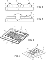
- Figure 1 shows a device comprising two dice 1, of semiconductor material, each integrating an own power component, an integrated circuit, or any other electronic or micro-electro-mechanical element.
- the dice 1 are bonded to a support 3, for example a printed-circuit board, typically of insulating material, carrying contact regions 4, of conductive material, for example metal, such as copper.
- the dice 1 are attached to the support 3 by bonding regions 5, for example conductive or non-conductive solder bonding regions.
- the dice 1 are connected to respective contact regions 4 by first wires 7 (one is represented for each die 1); moreover, the dice 1 are connected together through second wires 8.
- Figure 2 shows another system where two dice (designated again by 1) are connected together.
- Wires are generally of aluminium and are bonded by soldering; clips are generally of copper or bronze to be sufficiently stiff in the elastic domain. Bonding may be fusion soldering or powder soldering (sintering).
- Figures 3-6 show specific embodiments of the connection shown in Figure 2 .
- two dice 11 are attached to a support 12, here a DBC (Direct-Bonded Copper) multilayer, by a bonding layer 13.
- top surface of a die 17 is connected to external contact regions 18 by top clips 19.
- a bottom clip 20 couples the bottom surface of the die 17 to a plate 22 bonded to a support 23.
- the clips 19, 20 are generally pre-folded from a plane strip so as to form a plurality of bends.
- Figure 5 shows a die 25, bonded by a bottom solder layer 27 to a support 26 that is part of a metal leadframe also forming a first and a second external contact region 30, 33.
- the metal clip 29 comprises a first plane portion 29A bonded to the power die 25 by a top solder layer 28, of conductive material, which occupies a fair amount of the area of the die 25, and a second plane portion 29B, bonded to the first contact region 30 by a further solder layer 31, which is also of conductive material.
- a wire 32 of aluminium, connects a different portion of the surface of the power die 25 to the second external contact region 33 and has a current capacity lower than the metal clip 29.
- Figure 6 shows fixing of a die 35 to a ceramic support 36 formed as multilayer.
- the support 36 has a top layer 40 that is conductive, for example coated with silver alloy, and shaped to form external contact regions 41A and a die contact region 41B.
- the die 35 is fixed to the die contact region 41B by a first adhesive region 42 formed by a pre-applied sinter paste.
- a second adhesive region 43 is applied between the top surface of the die 35 and a copper foil 45 having a plating, for example NiPdAu plating (not represented) .
- Power bonding wires 46, of copper are soldered to the copper foil 45 and to some of the external contact regions 41B, for electrical connection of the die 35.
- a further bonding wire 47, of aluminium connects a contact pad 48 of the die 35 to a respective external contact region 41A.
- connections obtained by soldering have a greater resilience as compared to connections obtained by sintering, but neither of the two techniques provides sufficient reliability in some applications, for example in the automotive sector.
- US 2005/230820 discloses a power semiconductor arrangement comprising a substrate, a heat sink attached to one side of the substrate, a semiconductor component arranged on another side of the substrate and a resilient clip attached to the heat sink.
- US 2009/067131 discloses an electronic device mounting structure including elastic biasing members having a pressing member formed by a flat portion in contact with an electronic device and leg portions. The length of the leg portions is adjusted according to the height of the electronic device; the elastic biasing members are screwed to a wall member of a base plate.
- US 2019/333874 discloses a semiconductor device comprising a flat clip connected to a surface of a die and having a bent end for electrical connection to a lead.
- the clip may have a downwardly protruding portion.
- EP 2 372 763 discloses clips similar to those shown in Figure 4 .
- the aim of the present invention is to provide a solution for electrically connecting semiconductor dice and devices, overcoming the drawbacks of the prior art.
- a connecting strip, an electronic device, and a bonding method are provided, as defined in the attached claims.
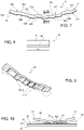
- Figures 7-9 show a connecting strip 50, also called clip, usable for electrical connection of one or more semiconductor dice together and/or to contact regions.
- the semiconductor die or dice may integrate a discrete electronic component, an electrical circuit or other electronic and/or micro-electro-mechanical component.
- at least one of the dice integrates a power component and/or a high-current component.
- the die or dice may integrate power devices such as IGBTs, diodes, high-voltage or low-voltage MOS transistors, silicon-based or silicon-carbide-based devices.
- the connecting strip 50 is used to contact two dice (designated by 72, 73 in Figures 10-13 ) together and to a support 70; however, the connecting strip 50 may be used for contacting a single die to one or more contact regions on a support or simply for coupling a number of dice together.
- the connecting strip 50 is of a conductive elastic material, and has an elongated shape, folded so as to define an overall arched or bowed shape.
- the connecting strip 50 In the undeformed condition, prior to welding to the support 70, the connecting strip 50 has a concave side 50A and a convex side 50B and is designed to be fixed to the support 70 on its convex side 50B, as discussed in greater detail hereinafter.
- the connecting strip 50 has ends 51 and is designed to be fixed to the support 70 at the ends 51 so as to block the dice 72, 73 against the support 70.
- the connecting strip 50 is formed by a sequence of flat portions. Also the ends 51 are flat so as to enable welding.
- the connecting strip 50 has, at least on the convex side 50B, projecting areas and recessed areas.
- both the concave side 50A and the convex side 50B have projecting areas and recessed areas.
- each projecting area 52A on the concave side 50A corresponds to a recessed area 53B on the convex side 50B and each recessed area 52A on the concave side 50A corresponds a projecting area 52B on the convex side 50B.
- the convex side 50B has four projecting areas 52B, interspersed with three recessed areas 53B; the projecting areas 52B on the convex side 50B correspond to recessed areas 53A on the concave side 50A.
- the ends 51 are formed by projecting areas 52B on the convex side 50B.
- the projecting areas 52B on the convex side 50B are approximately flat, so that they can be pressed flat down against contact pads (see Figure 11 ) on the surface of the dice 72, 73 and on the support 70, as explained hereinafter.
- the connecting strip 50 of Figures 7 and 8 is formed by an elastic body 61 coated by a contact layer 62.
- the elastic body 61 may be copper or a copper alloy, such as bronze, and have a rectangular cross-section (see Figure 8 ) with a thickness comprised between 300 ⁇ m and 1 mm, in particular between 300 and 800 ⁇ m.
- the contact layer 62 is of a softer material than the elastic body 61; for example, it may be aluminium and have a thickness smaller than the thickness of the elastic body 61, for example comprised between 50 ⁇ m and 100 ⁇ m. Alternatively, it could be a silver alloy, with a thickness comprised between 3 and 5 ⁇ m.
- the connecting strip 50 may have a width W ( Figure 8 ) comprised between 2 and 5 mm.
- the connecting strip 50 may be manufactured by hot laminating an aluminium layer on copper or bronze and cutting it into strips, which are then wound in a coil. The coil is then folded to obtain the projecting areas and the recessed areas 52A, 52B, 53A, 53B and singulated.
- the connecting strip 50 is represented with a solid line in the undeformed condition, prior to bonding to the support 70, and with a dashed line in the deformed condition, after bonding to the support 70.
- the support 70 is here formed by a multilayer, for example a DBC (Direct-Bonded Copper) multilayer, and the two dice 72, 73 have already been attached thereon.
- a multilayer for example a DBC (Direct-Bonded Copper) multilayer
- the substrate 70 comprises a bottom layer 80, of conductive material such as copper; an intermediate layer 81, electrically insulating and typically ceramic material, such as alumina (Al 2 O 3 ) or aluminium nitride (AlN); and a top layer 82, of conductive material, such as copper.
- the top layer 82 is suitably shaped to form contact regions.
- the top layer 82 forms a die contact region, designated by 83A, and the dice 72, 73 and two connection contact regions, designated by 83B, have been bonded thereon.
- the die contact region 83A and the connection contact regions 83B are aligned to each other, so that the connecting strip 50 can be arranged on, and in contact with, both the connection contact regions 83B and the dice 72, 73.
- the dice 72, 73 have contact pads 85 (in the example shown, the first die 72 has one contact pad 85 and the second die 73 has three contact pads 85); the contact pads 85 are typically of aluminium, for example with a thickness of 4-9 ⁇ m.
- the connecting strip 50 is arranged with the convex side 50B facing the support 70 and the dice 72, 73, and is welded to the support 70.
- the connecting strip 50 is arranged so that the projecting areas 52B on its convex side 50B are positioned at the dice 72 and 73 and, more precisely, at the contact pads 85, and that the ends 51 arrange at the connection contact regions 83B.
- the connecting strip 50 is pressed at the ends 51 and undergoes deformation, flattening out.
- the device formed by the dice 72, 73, by the support 70 and by the connecting strip 50, and designated by 95, may be packaged.
- the connecting strip 50 forms an electrical contact between the contact pads 85 of the dice 72 and 73 and the connection contact regions 83B of the support 70, without any intermediate bonding material being present between the connecting strip 50 and the dice 72, 73.
- the contact layer 62 undergoes deformation, adapting to the microstructure of the contact pads 85 of the dice 72, 73 (which may also in part deform), thus creating an intimate mechanical contact between them and therefore an optimal electrical contact.
- Bonding of the connecting strip 50 may be performed by ultrasonic technology, as described below with reference to Figures 12-13 .
- bonding may be performed using an ultrasonic apparatus such as an ultrasonic welding sonotrode having a welding head 90.
- the welding head 90 may have a handling system, for example a suction system, for picking up and holding the connecting strip 50 and has a useful width approximately equal to the connecting strip 50.
- the welding head 90 has welding portions 91 arranged at a distance so as to position themselves at the ends 51 of the connecting strip 50 and to exert a pressure on these ends 51 during welding.
- the welding portions 91 of the welding head 90 may be of tungsten carbide and apply a pressure comprised between 3 MPa and 5 MPa at 50 kHz. Welding may be performed at room temperature; in this way, any possible heat that develops (generally lower than 200°C) does not damage the dice 72, 73, in particular if they are made using silicon-carbide technology. Moreover, since the bonding pressure is applied only on the ends 51 of the connecting strip 50, and the only pressure acting on the dice 72, 73 is the elastic pressure due to the connecting strip 50 after bonding, the dice 72, 73 are not damaged.
- the connecting strip 50 and the device 95 described herein have many advantages.
- the connecting strip 50 can in fact be manufactured at a reduced cost and has high endurance and reliability. It is able to carry high currents, minimizing parasitic effects, has high temperature resistance, and can be simply bonded, using ultrasonic techniques but also by sintering.
- the device 95 including the connecting strip 50, has high reliability and strength of the connections.
- the die or dice are held in an elastic, non-plastic way, therefore blocking is particularly resistant to vibrations and mechanical stresses even over time.
- the contact pads 85 are in contact with portions of the same material as the contact layer 62, there are no differences of thermal coefficient between them, thus eliminating any cause of failure in case of thermal stresses as a result of the different coefficients of thermal expansion (CTE).
- the elastic stress generated by deformation keeps the connecting strip 50 in contact with the contact pads 85 of the dice 72, 73 in a reliable way over time.
- the bonding process may be carried out at reduced costs, in particular as compared to known wet metal process described above.
- the present connecting strip is of conductive elastic material, and is generally arch-shaped, with a general concave side and a general convex side, the general concave side and the general convex side being opposite to each other, the connecting strip comprising flat bonding ends on each end of the generally arch-shaped connecting strip.
- the connecting strip is configured to be flattened out during bonding to a support and so provide a pressure contact between the support and the die.Finally, it is clear that modifications and variations may be made to the connecting strip, to the electronic device and to the electrical connection method described and shown herein, without thereby departing from the scope of the present invention, as defined in the attached claims.
- the connecting strip may be of other conductive elastic materials; bonding the ends may be obtained by sintering, instead of by ultrasonic welding; the die may integrate electronic components and circuits of different types or be formed by packaged devices having external contact regions to be electrically connected in complex systems and/or to supports.
- the elastic body 61 may be coated by the contact layer only in some portions, for example in the contact area with the die or dice 72, 73 and at the ends 51.
- the die might not be soldered but held in contact with the support only by the elastic force of the connecting strip.
Landscapes
- Cooling Or The Like Of Semiconductors Or Solid State Devices (AREA)
- Structures For Mounting Electric Components On Printed Circuit Boards (AREA)
- Connections Effected By Soldering, Adhesion, Or Permanent Deformation (AREA)
- Coupling Device And Connection With Printed Circuit (AREA)
- Details Of Connecting Devices For Male And Female Coupling (AREA)
Abstract
Description
- The present invention relates to a connecting strip for discrete and/or power electronic devices and a discrete and/or power electronic device coupled by the strip.
- As is known, dice of semiconductor material integrating electronic devices (whether they are discrete components, more complex circuits or micro-electro-mechanical components) are bonded to a support carrying connection regions and are electrically connected to these connection regions and possibly to other power or discrete devices through connection structures formed by wires or conductive strips (so-called clips).
- When the electronic device is a power device, the connection structures are designed to have a current capacity that is adequate with respect to the required current. These connection structures are moreover designed to have an adequate endurance taking into account the application and the specific operating conditions.
- For instance,
Figure 1 shows a device comprising twodice 1, of semiconductor material, each integrating an own power component, an integrated circuit, or any other electronic or micro-electro-mechanical element. Thedice 1 are bonded to asupport 3, for example a printed-circuit board, typically of insulating material, carryingcontact regions 4, of conductive material, for example metal, such as copper. Thedice 1 are attached to thesupport 3 bybonding regions 5, for example conductive or non-conductive solder bonding regions. - In
Figure 1 , thedice 1 are connected torespective contact regions 4 by first wires 7 (one is represented for each die 1); moreover, thedice 1 are connected together throughsecond wires 8. -
Figure 2 shows another system where two dice (designated again by 1) are connected together. Wires are generally of aluminium and are bonded by soldering; clips are generally of copper or bronze to be sufficiently stiff in the elastic domain. Bonding may be fusion soldering or powder soldering (sintering). -
Figures 3-6 show specific embodiments of the connection shown inFigure 2 . - For instance, in
Figure 3 , twodice 11 are attached to asupport 12, here a DBC (Direct-Bonded Copper) multilayer, by abonding layer 13. The top layer of thesupport 12, appropriately shaped, forms adie contact region 15 andexternal contact regions 16.Wires 14, of variable thickness, according to the desired current capacity, couple thedice 11 together and to theexternal contact regions 16. - In
Figure 4 , the top surface of a die 17 is connected toexternal contact regions 18 bytop clips 19. Abottom clip 20 couples the bottom surface of the die 17 to aplate 22 bonded to asupport 23. Theclips -
Figure 5 shows adie 25, bonded by abottom solder layer 27 to asupport 26 that is part of a metal leadframe also forming a first and a secondexternal contact region metal clip 29, typically of copper, electrically connects the power die 25 to the firstexternal contact region 30. Themetal clip 29 comprises afirst plane portion 29A bonded to the power die 25 by atop solder layer 28, of conductive material, which occupies a fair amount of the area of the die 25, and asecond plane portion 29B, bonded to thefirst contact region 30 by afurther solder layer 31, which is also of conductive material. Awire 32, of aluminium, connects a different portion of the surface of the power die 25 to the secondexternal contact region 33 and has a current capacity lower than themetal clip 29. -
Figure 6 shows fixing of a die 35 to aceramic support 36 formed as multilayer. Specifically, thesupport 36 has atop layer 40 that is conductive, for example coated with silver alloy, and shaped to formexternal contact regions 41A and adie contact region 41B. The die 35 is fixed to the diecontact region 41B by a firstadhesive region 42 formed by a pre-applied sinter paste. A secondadhesive region 43 is applied between the top surface of thedie 35 and acopper foil 45 having a plating, for example NiPdAu plating (not represented) .Power bonding wires 46, of copper, are soldered to thecopper foil 45 and to some of theexternal contact regions 41B, for electrical connection of thedie 35. Afurther bonding wire 47, of aluminium, connects acontact pad 48 of the die 35 to a respectiveexternal contact region 41A. - In all the shown electrical connection solutions, the problem of endurance of the soldering exists. In fact, because of the different coefficient of thermal expansion (CTE) between the bonding wires or clips and the silicon die, the soldering may be subject to degradation and the wire or clip may detach (bond off phenomenon), in particular in case of thermal variations and/or mechanical stresses.
- Generally, it has been seen that connections obtained by soldering have a greater resilience as compared to connections obtained by sintering, but neither of the two techniques provides sufficient reliability in some applications, for example in the automotive sector.
- To improve adhesion and endurance, techniques have been developed based upon wet metal, i.e., the forming a stack of metal layers (typically Ti-Ni-Au or Ag), which enables the top part of the die to be wettable and solderable to a clip. Such a stack of materials may be formed also on the rear side of the die, to be able to bond it to the
support 36. These techniques are, however, costly and involve the use of a costly soldering material. -
US 2005/230820 discloses a power semiconductor arrangement comprising a substrate, a heat sink attached to one side of the substrate, a semiconductor component arranged on another side of the substrate and a resilient clip attached to the heat sink. -
US 2009/067131 discloses an electronic device mounting structure including elastic biasing members having a pressing member formed by a flat portion in contact with an electronic device and leg portions. The length of the leg portions is adjusted according to the height of the electronic device; the elastic biasing members are screwed to a wall member of a base plate. -
US 2019/333874 discloses a semiconductor device comprising a flat clip connected to a surface of a die and having a bent end for electrical connection to a lead. The clip may have a downwardly protruding portion. -
EP 2 372 763 discloses clips similar to those shown inFigure 4 . - The aim of the present invention is to provide a solution for electrically connecting semiconductor dice and devices, overcoming the drawbacks of the prior art.
- According to the present invention a connecting strip, an electronic device, and a bonding method are provided, as defined in the attached claims.
- For a better understanding of the present invention, an embodiment thereof is now described purely by way of nonlimiting example, with reference to the attached drawings, wherein:
-
Figure 1 is a side view of a system formed by two semiconductor dice; -
Figure 2 is a side view of another system formed by two semiconductor dice; -
Figure 3 is a perspective view of an electrical connection solution for the semiconductor dice ofFigure 2 ; -
Figure 4 is a perspective view of another electrical connection solution for the semiconductor dice ofFigure 2 ; -
Figure 5 is a side view showing another possibility for connection a semiconductor die; -
Figure 6 is a perspective view of a semiconductor die; -
Figure 7 is a side view of a strip that can be used for electrical connection of an electronic device; -
Figure 8 is a cross-section of the connecting strip ofFigure 7 , taken along section line VIII-VIII ofFigure 7 ; -
Figure 9 is a perspective bottom view of the connecting strip ofFigure 7 ; -
Figure 10 is a side view of the connecting strip ofFigure 7 , in two steps of bonding to a support; -
Figure 11 is a perspective view of a shaped support usable for connection of a power device; -
Figure 12 is a perspective view of the steps of welding the connecting strip ofFigure 7 to the support ofFigure 11 ; and -
Figure 13 is a side view of the welding steps ofFigure 12 . -
Figures 7-9 show a connectingstrip 50, also called clip, usable for electrical connection of one or more semiconductor dice together and/or to contact regions. The semiconductor die or dice may integrate a discrete electronic component, an electrical circuit or other electronic and/or micro-electro-mechanical component. Typically, at least one of the dice integrates a power component and/or a high-current component. For instance, the die or dice may integrate power devices such as IGBTs, diodes, high-voltage or low-voltage MOS transistors, silicon-based or silicon-carbide-based devices. - In the embodiment shown in
Figures 7-13 , the connectingstrip 50 is used to contact two dice (designated by 72, 73 inFigures 10-13 ) together and to asupport 70; however, the connectingstrip 50 may be used for contacting a single die to one or more contact regions on a support or simply for coupling a number of dice together. - In detail, the connecting
strip 50 is of a conductive elastic material, and has an elongated shape, folded so as to define an overall arched or bowed shape. - In the undeformed condition, prior to welding to the
support 70, the connectingstrip 50 has aconcave side 50A and aconvex side 50B and is designed to be fixed to thesupport 70 on itsconvex side 50B, as discussed in greater detail hereinafter. - The connecting
strip 50 hasends 51 and is designed to be fixed to thesupport 70 at theends 51 so as to block thedice support 70. - In the embodiment shown, the connecting
strip 50 is formed by a sequence of flat portions. Also the ends 51 are flat so as to enable welding. - In detail, the connecting
strip 50 has, at least on theconvex side 50B, projecting areas and recessed areas. In the embodiment shown, both theconcave side 50A and theconvex side 50B have projecting areas and recessed areas. - In particular, the projecting areas and the recessed areas on the
concave side 50A are designated by 52A and by 53A, respectively; the projecting areas and the recessed areas on theconvex side 50B are designated by 52B and by 53B, respectively. In addition, each projectingarea 52A on theconcave side 50A corresponds to a recessedarea 53B on theconvex side 50B and each recessedarea 52A on theconcave side 50A corresponds a projectingarea 52B on theconvex side 50B. - In particular, in
Figure 7 , wherein the connectingstrip 50 is designed to contact four contact pads, arranged on two different dice (as described hereinafter with reference toFigure 11 ), theconvex side 50B has four projectingareas 52B, interspersed with three recessedareas 53B; the projectingareas 52B on theconvex side 50B correspond to recessedareas 53A on theconcave side 50A. - Here, the ends 51 are formed by projecting
areas 52B on theconvex side 50B. - The projecting
areas 52B on theconvex side 50B are approximately flat, so that they can be pressed flat down against contact pads (seeFigure 11 ) on the surface of thedice support 70, as explained hereinafter. - The connecting
strip 50 ofFigures 7 and 8 is formed by anelastic body 61 coated by acontact layer 62. - The
elastic body 61 may be copper or a copper alloy, such as bronze, and have a rectangular cross-section (seeFigure 8 ) with a thickness comprised between 300 µm and 1 mm, in particular between 300 and 800 µm. - The
contact layer 62 is of a softer material than theelastic body 61; for example, it may be aluminium and have a thickness smaller than the thickness of theelastic body 61, for example comprised between 50 µm and 100 µm. Alternatively, it could be a silver alloy, with a thickness comprised between 3 and 5 µm. - The connecting
strip 50 may have a width W (Figure 8 ) comprised between 2 and 5 mm. - The connecting
strip 50 may be manufactured by hot laminating an aluminium layer on copper or bronze and cutting it into strips, which are then wound in a coil. The coil is then folded to obtain the projecting areas and the recessedareas - In
Figure 10 , the connectingstrip 50 is represented with a solid line in the undeformed condition, prior to bonding to thesupport 70, and with a dashed line in the deformed condition, after bonding to thesupport 70. - The
support 70 is here formed by a multilayer, for example a DBC (Direct-Bonded Copper) multilayer, and the twodice - In the example shown (see also
Figure 11 ), thesubstrate 70 comprises abottom layer 80, of conductive material such as copper; anintermediate layer 81, electrically insulating and typically ceramic material, such as alumina (Al2O3) or aluminium nitride (AlN); and atop layer 82, of conductive material, such as copper. Thetop layer 82 is suitably shaped to form contact regions. In the example shown, thetop layer 82 forms a die contact region, designated by 83A, and thedice - The
die contact region 83A and theconnection contact regions 83B are aligned to each other, so that the connectingstrip 50 can be arranged on, and in contact with, both theconnection contact regions 83B and thedice - The
dice first die 72 has onecontact pad 85 and thesecond die 73 has three contact pads 85); thecontact pads 85 are typically of aluminium, for example with a thickness of 4-9 µm. - As mentioned above and may be seen in
Figure 10 , the connectingstrip 50 is arranged with theconvex side 50B facing thesupport 70 and thedice support 70. - In particular, the connecting
strip 50 is arranged so that the projectingareas 52B on itsconvex side 50B are positioned at thedice contact pads 85, and that the ends 51 arrange at theconnection contact regions 83B. In order to enable welding, the connectingstrip 50 is pressed at theends 51 and undergoes deformation, flattening out. - After welding, the device formed by the
dice support 70 and by the connectingstrip 50, and designated by 95, may be packaged. - In this way, the connecting
strip 50 forms an electrical contact between thecontact pads 85 of thedice connection contact regions 83B of thesupport 70, without any intermediate bonding material being present between the connectingstrip 50 and thedice - Because of bonding, and as a result of the elastic pressure exerted by the connecting
strip 50, and specifically by the projectingareas 52B (Figures 7 and 9 ), on thecontact pads 85, thecontact layer 62 undergoes deformation, adapting to the microstructure of thecontact pads 85 of thedice 72, 73 (which may also in part deform), thus creating an intimate mechanical contact between them and therefore an optimal electrical contact. - Bonding of the connecting
strip 50 may be performed by ultrasonic technology, as described below with reference toFigures 12-13 . - In particular, bonding may be performed using an ultrasonic apparatus such as an ultrasonic welding sonotrode having a
welding head 90. - The
welding head 90 may have a handling system, for example a suction system, for picking up and holding the connectingstrip 50 and has a useful width approximately equal to the connectingstrip 50. In particular, thewelding head 90 haswelding portions 91 arranged at a distance so as to position themselves at theends 51 of the connectingstrip 50 and to exert a pressure on theseends 51 during welding. - For instance, the
welding portions 91 of thewelding head 90 may be of tungsten carbide and apply a pressure comprised between 3 MPa and 5 MPa at 50 kHz. Welding may be performed at room temperature; in this way, any possible heat that develops (generally lower than 200°C) does not damage thedice ends 51 of the connectingstrip 50, and the only pressure acting on thedice strip 50 after bonding, thedice - The connecting
strip 50 and thedevice 95 described herein have many advantages. - The connecting
strip 50 can in fact be manufactured at a reduced cost and has high endurance and reliability. It is able to carry high currents, minimizing parasitic effects, has high temperature resistance, and can be simply bonded, using ultrasonic techniques but also by sintering. - The
device 95, including the connectingstrip 50, has high reliability and strength of the connections. - In fact, the die or dice are held in an elastic, non-plastic way, therefore blocking is particularly resistant to vibrations and mechanical stresses even over time.
- Furthermore, since no bonding material is provided between the connecting
strip 50 and thedice strip 50, there are no regions that can undergo degradation in case of temperature changes, in particular of temperature swings, as for wire bonding or soldering with or without addition of material, but between different material. - Since the
contact pads 85, of aluminium, are in contact with portions of the same material as thecontact layer 62, there are no differences of thermal coefficient between them, thus eliminating any cause of failure in case of thermal stresses as a result of the different coefficients of thermal expansion (CTE). - The elastic stress generated by deformation keeps the connecting
strip 50 in contact with thecontact pads 85 of thedice - The bonding process may be carried out at reduced costs, in particular as compared to known wet metal process described above.
- In practice, the present connecting strip is of conductive elastic material, and is generally arch-shaped, with a general concave side and a general convex side, the general concave side and the general convex side being opposite to each other, the connecting strip comprising flat bonding ends on each end of the generally arch-shaped connecting strip.
- The connecting strip is configured to be flattened out during bonding to a support and so provide a pressure contact between the support and the die.Finally, it is clear that modifications and variations may be made to the connecting strip, to the electronic device and to the electrical connection method described and shown herein, without thereby departing from the scope of the present invention, as defined in the attached claims.
- For instance, the connecting strip may be of other conductive elastic materials; bonding the ends may be obtained by sintering, instead of by ultrasonic welding; the die may integrate electronic components and circuits of different types or be formed by packaged devices having external contact regions to be electrically connected in complex systems and/or to supports.
- Moreover, the
elastic body 61 may be coated by the contact layer only in some portions, for example in the contact area with the die ordice - For instance, the die might not be soldered but held in contact with the support only by the elastic force of the connecting strip.
Claims (15)
- A connecting strip (50) of conductive elastic material, the connecting strip (50) being generally arch-shaped, with a general concave side (50A) and a general convex side (50B), the general concave side (50A) and the general convex side (50B) being opposite to each other, the connecting strip (50) comprising flat bonding ends (51) on each end of the generally arch-shaped connecting strip (50).
- The connecting strip according to the preceding claim, wherein the general convex side (50B) has at least one die connection projecting area (52B), two support connection projecting areas (51) and two recessed areas (53B), the support connection projecting areas forming the connection ends (51) of the connecting strip (50), and wherein each recessed area (53B) extends between the die connection projecting area (52B) and a respective support connection projecting area (51).
- The connecting strip according to claim 1 or 2, comprising an elastic body (61) coated on one side with a contact layer (62).
- The connecting strip according to the preceding claim, wherein the elastic body (61) is of copper or a copper alloy, such as bronze.
- The connecting strip according to claim 3 or 4, wherein the contact layer (62) is of a softer material than the elastic body (61), in particular aluminium or silver alloy.
- The connecting strip according to the preceding claim, wherein the elastic body (61) has a thickness comprised between 300 µm and 1 mm and the contact layer (62) has a thickness comprised between 50 and 100 µm in the case of aluminium and 3-5 µm in the case of silver alloy.
- The connecting strip according to any of the preceding claims, configured to be flattened out during bonding to a support (70) and so provide a pressure contact between the support (70) and at least one die (72, 73) arranged between the connecting strip (50) and the support (70) .
- An electronic device, comprising a support (70), at least one die (72, 73) including semiconductor material, and a connecting strip (50), wherein the connecting strip (50) is of conductive elastic material, having a first side and a second side (50B, 50A), the first side (50B) being in contact with the at least one die (72, 73) and pressing the at least one die (72, 73) against the support (70), and wherein the connecting strip (50) further comprises flat bonding ends (51) bonded to the support (70) and elastically presses against the at least one die, thus electrically connecting the at least one die (72, 73) to the support (70).
- The electronic device according to the preceding claim, wherein the first side (50B) of the connecting strip (50) has at least one die connection projecting area (52B), two support connection projecting areas (51), and two recessed areas (53B), the support connection projecting areas forming the connection ends (51) of the connecting strip (50), each recessed area (53B) extending between the die connection projecting area (52B) and a respective support connection projecting area (51), and wherein the die connection projecting area is in elastic and electrical contact with the at least one die (72, 73).
- The electronic device according to claim 8 or 9, wherein the connecting strip (50) comprises an elastic body (61) coated on one side by a contact layer (62), wherein the contact layer (62) is in elastic and electrical contact with the at least one die (72, 73) and defines the first side (50B) of the connecting strip.
- The electronic device according to the preceding claim, wherein the elastic body (61) is of copper or a copper alloy, such as bronze, and the contact layer (62) is of aluminium or silver alloy.
- The electronic device according to the preceding claim, wherein the contact layer (62) has a smaller thickness than the elastic body (61).
- A method for bonding at least one die (72, 73) to a support (70) by a connecting strip (50), the at least one die (72, 73) comprising semiconductor material, and the connecting strip (50) being of conductive elastic material, being generally arch-shaped, with a general concave side and a general convex side (50A, 50B), the general concave side (50A) and the general convex side (50B) being opposite to each other, the connecting strip (50) having bonding ends (51) on each end of the generally arch-shaped connecting strip (50), the method comprising:arranging the at least one die (72, 73) on the support (70);arranging the connecting strip (50) on the at least one die (72, 73), with the convex side (50B) facing the at least one die;flattening the connecting strip (50) so as to bring the bonding ends (51) into contact with the support (70), andbonding the bonding ends (51) of the connecting strip (50) to the support (70) so that the connecting strip (50) is in direct electrical contact with the at least one die (72, 73) and elastically presses it against the support (70).
- The method according to the preceding claim, wherein bonding the bonding ends (51) comprises ultrasonic welding.
- The method according to claim 13, wherein bonding the bonding ends (51) comprises sintering.
Applications Claiming Priority (1)
| Application Number | Priority Date | Filing Date | Title |
|---|---|---|---|
| IT102021000008036A IT202100008036A1 (en) | 2021-03-31 | 2021-03-31 | CONNECTOR STRIP FOR DISCRETE AND/OR POWER ELECTRONIC DEVICES AND THE DISCRETE AND/OR POWER ELECTRONIC DEVICE CONNECTED THROUGH SUCH CONNECTOR STRIP |
Publications (2)
| Publication Number | Publication Date |
|---|---|
| EP4068351A2 true EP4068351A2 (en) | 2022-10-05 |
| EP4068351A3 EP4068351A3 (en) | 2023-06-07 |
Family
ID=76270014
Family Applications (1)
| Application Number | Title | Priority Date | Filing Date |
|---|---|---|---|
| EP22165630.9A Pending EP4068351A3 (en) | 2021-03-31 | 2022-03-30 | Connecting strip for discrete or power electronic devices and a connection method using the same |
Country Status (3)
| Country | Link |
|---|---|
| US (1) | US12374648B2 (en) |
| EP (1) | EP4068351A3 (en) |
| IT (1) | IT202100008036A1 (en) |
Families Citing this family (1)
| Publication number | Priority date | Publication date | Assignee | Title |
|---|---|---|---|---|
| US20240404982A1 (en) * | 2023-06-02 | 2024-12-05 | Infineon Technologies Ag | Power semiconductor module having a metallic clip with ultrasonically welded contact regions and method of producing the power semiconductor module |
Citations (4)
| Publication number | Priority date | Publication date | Assignee | Title |
|---|---|---|---|---|
| US20050230820A1 (en) | 2004-04-16 | 2005-10-20 | Thomas Licht | Power semiconductor arrangement |
| US20090067131A1 (en) | 2007-09-12 | 2009-03-12 | Denso Corporation | Electronic device mounting structure |
| EP2372763A2 (en) | 2010-04-02 | 2011-10-05 | Hitachi Ltd. | Power semiconductor module |
| US20190333874A1 (en) | 2018-04-26 | 2019-10-31 | Infineon Technologies Ag | Semiconductor device comprising a composite material clip |
Family Cites Families (4)
| Publication number | Priority date | Publication date | Assignee | Title |
|---|---|---|---|---|
| US20040217488A1 (en) * | 2003-05-02 | 2004-11-04 | Luechinger Christoph B. | Ribbon bonding |
| US8164176B2 (en) * | 2006-10-20 | 2012-04-24 | Infineon Technologies Ag | Semiconductor module arrangement |
| US8022558B2 (en) * | 2009-02-13 | 2011-09-20 | Infineon Technologies Ag | Semiconductor package with ribbon with metal layers |
| US10242938B2 (en) * | 2017-05-16 | 2019-03-26 | Infineon Technologies Americas Corp. | Integrated shunt in circuit package |
-
2021
- 2021-03-31 IT IT102021000008036A patent/IT202100008036A1/en unknown
-
2022
- 2022-03-22 US US17/701,352 patent/US12374648B2/en active Active
- 2022-03-30 EP EP22165630.9A patent/EP4068351A3/en active Pending
Patent Citations (4)
| Publication number | Priority date | Publication date | Assignee | Title |
|---|---|---|---|---|
| US20050230820A1 (en) | 2004-04-16 | 2005-10-20 | Thomas Licht | Power semiconductor arrangement |
| US20090067131A1 (en) | 2007-09-12 | 2009-03-12 | Denso Corporation | Electronic device mounting structure |
| EP2372763A2 (en) | 2010-04-02 | 2011-10-05 | Hitachi Ltd. | Power semiconductor module |
| US20190333874A1 (en) | 2018-04-26 | 2019-10-31 | Infineon Technologies Ag | Semiconductor device comprising a composite material clip |
Also Published As
| Publication number | Publication date |
|---|---|
| IT202100008036A1 (en) | 2022-10-01 |
| US20220320032A1 (en) | 2022-10-06 |
| US12374648B2 (en) | 2025-07-29 |
| EP4068351A3 (en) | 2023-06-07 |
Similar Documents
| Publication | Publication Date | Title |
|---|---|---|
| US6881071B2 (en) | Power semiconductor module with pressure contact means | |
| CN109478521B (en) | Semiconductor device with a plurality of semiconductor chips | |
| JP4635564B2 (en) | Semiconductor device | |
| JP5665729B2 (en) | Power semiconductor device | |
| JP6012533B2 (en) | Power semiconductor device | |
| WO1999052147A1 (en) | Wire bond attachment of a integrated circuit package to a heat sink | |
| JPH10335579A (en) | High power semiconductor module device | |
| JP6627600B2 (en) | Power module manufacturing method | |
| JPH10154774A (en) | Semiconductor module | |
| US20230352362A1 (en) | Power semiconductor module comprising at least one power semiconductor element | |
| US20250323205A1 (en) | Connecting strip for discrete and power electronic devices | |
| US20220302072A1 (en) | Semiconductor module comprising a semiconductor and comprising a shaped metal body that is electrically contacted by the semiconductor | |
| US20190356098A1 (en) | Method for Bonding an Electrically Conductive Element to a Bonding Partner | |
| US12374648B2 (en) | Connecting strip for discrete and power electronic devices | |
| EP3863045B1 (en) | Power semiconductor module arrangement and method for producing the same | |
| JPH10144967A (en) | Thermoelectric element module for cooling | |
| EP4239660A1 (en) | Method of attaching a terminal to a metal substrate structure for a semiconductor power module and semiconductor power module | |
| JP7026688B2 (en) | Semiconductor module and manufacturing method including first and second connecting elements for connecting semiconductor chips | |
| CN118235233A (en) | Semiconductor device and method for manufacturing semiconductor device | |
| EP4510184A1 (en) | Terminal element, and power semiconductor module arrangement comprising a terminal element | |
| CN114203659A (en) | Multilayer interconnection tape | |
| CN115621232B (en) | Power semiconductor device packaging structure and power semiconductor device module | |
| US20240312880A1 (en) | Semiconductor device, method of manufacturing the same, and power conversion device | |
| JPH08125092A (en) | Semiconductor device and manufacturing method thereof | |
| KR101104389B1 (en) | Termination Structure of Semiconductor Chip |
Legal Events
| Date | Code | Title | Description |
|---|---|---|---|
| PUAI | Public reference made under article 153(3) epc to a published international application that has entered the european phase |
Free format text: ORIGINAL CODE: 0009012 |
|
| STAA | Information on the status of an ep patent application or granted ep patent |
Free format text: STATUS: THE APPLICATION HAS BEEN PUBLISHED |
|
| AK | Designated contracting states |
Kind code of ref document: A2 Designated state(s): AL AT BE BG CH CY CZ DE DK EE ES FI FR GB GR HR HU IE IS IT LI LT LU LV MC MK MT NL NO PL PT RO RS SE SI SK SM TR |
|
| PUAL | Search report despatched |
Free format text: ORIGINAL CODE: 0009013 |
|
| AK | Designated contracting states |
Kind code of ref document: A3 Designated state(s): AL AT BE BG CH CY CZ DE DK EE ES FI FR GB GR HR HU IE IS IT LI LT LU LV MC MK MT NL NO PL PT RO RS SE SI SK SM TR |
|
| RIC1 | Information provided on ipc code assigned before grant |
Ipc: H01L 25/07 20060101ALI20230428BHEP Ipc: H01L 21/60 20060101ALI20230428BHEP Ipc: H01L 23/48 20060101AFI20230428BHEP |
|
| STAA | Information on the status of an ep patent application or granted ep patent |
Free format text: STATUS: REQUEST FOR EXAMINATION WAS MADE |
|
| 17P | Request for examination filed |
Effective date: 20231205 |
|
| RBV | Designated contracting states (corrected) |
Designated state(s): AL AT BE BG CH CY CZ DE DK EE ES FI FR GB GR HR HU IE IS IT LI LT LU LV MC MK MT NL NO PL PT RO RS SE SI SK SM TR |
|
| REG | Reference to a national code |
Ref country code: DE Ref legal event code: R079 Free format text: PREVIOUS MAIN CLASS: H01L0023480000 Ipc: H10W0072000000 |
|
| RIC1 | Information provided on ipc code assigned before grant |
Ipc: H10W 72/00 20260101AFI20260127BHEP Ipc: H10W 90/00 20260101ALI20260127BHEP Ipc: H10W 72/90 20260101ALI20260127BHEP Ipc: H10W 72/60 20260101ALI20260127BHEP Ipc: H10W 72/50 20260101ALI20260127BHEP Ipc: H10W 99/00 20260101ALI20260127BHEP |
|
| GRAP | Despatch of communication of intention to grant a patent |
Free format text: ORIGINAL CODE: EPIDOSNIGR1 |
|
| STAA | Information on the status of an ep patent application or granted ep patent |
Free format text: STATUS: GRANT OF PATENT IS INTENDED |