EP4067950B1 - Lichtwellenleiter und entsprechendes herstellungsverfahren - Google Patents
Lichtwellenleiter und entsprechendes herstellungsverfahren Download PDFInfo
- Publication number
- EP4067950B1 EP4067950B1 EP22164658.1A EP22164658A EP4067950B1 EP 4067950 B1 EP4067950 B1 EP 4067950B1 EP 22164658 A EP22164658 A EP 22164658A EP 4067950 B1 EP4067950 B1 EP 4067950B1
- Authority
- EP
- European Patent Office
- Prior art keywords
- microstructures
- optical guide
- piece
- extraction
- semi
- Prior art date
- Legal status (The legal status is an assumption and is not a legal conclusion. Google has not performed a legal analysis and makes no representation as to the accuracy of the status listed.)
- Active
Links
Images


Classifications
-
- G—PHYSICS
- G02—OPTICS
- G02B—OPTICAL ELEMENTS, SYSTEMS OR APPARATUS
- G02B6/00—Light guides; Structural details of arrangements comprising light guides and other optical elements, e.g. couplings
-
- G—PHYSICS
- G02—OPTICS
- G02B—OPTICAL ELEMENTS, SYSTEMS OR APPARATUS
- G02B27/00—Optical systems or apparatus not provided for by any of the groups G02B1/00 - G02B26/00, G02B30/00
- G02B27/01—Head-up displays
- G02B27/0101—Head-up displays characterised by optical features
-
- G—PHYSICS
- G02—OPTICS
- G02B—OPTICAL ELEMENTS, SYSTEMS OR APPARATUS
- G02B27/00—Optical systems or apparatus not provided for by any of the groups G02B1/00 - G02B26/00, G02B30/00
- G02B27/01—Head-up displays
- G02B27/017—Head mounted
- G02B27/0172—Head mounted characterised by optical features
-
- G—PHYSICS
- G02—OPTICS
- G02B—OPTICAL ELEMENTS, SYSTEMS OR APPARATUS
- G02B5/00—Optical elements other than lenses
- G02B5/18—Diffraction gratings
- G02B5/1847—Manufacturing methods
-
- G—PHYSICS
- G02—OPTICS
- G02B—OPTICAL ELEMENTS, SYSTEMS OR APPARATUS
- G02B5/00—Optical elements other than lenses
- G02B5/18—Diffraction gratings
- G02B5/1861—Reflection gratings characterised by their structure, e.g. step profile, contours of substrate or grooves, pitch variations, materials
-
- G—PHYSICS
- G02—OPTICS
- G02B—OPTICAL ELEMENTS, SYSTEMS OR APPARATUS
- G02B6/00—Light guides; Structural details of arrangements comprising light guides and other optical elements, e.g. couplings
- G02B6/0001—Light guides; Structural details of arrangements comprising light guides and other optical elements, e.g. couplings specially adapted for lighting devices or systems
- G02B6/0011—Light guides; Structural details of arrangements comprising light guides and other optical elements, e.g. couplings specially adapted for lighting devices or systems the light guides being planar or of plate-like form
- G02B6/0033—Means for improving the coupling-out of light from the light guide
- G02B6/0035—Means for improving the coupling-out of light from the light guide provided on the surface of the light guide or in the bulk of it
- G02B6/0036—2-D arrangement of prisms, protrusions, indentations or roughened surfaces
-
- G—PHYSICS
- G02—OPTICS
- G02B—OPTICAL ELEMENTS, SYSTEMS OR APPARATUS
- G02B6/00—Light guides; Structural details of arrangements comprising light guides and other optical elements, e.g. couplings
- G02B6/0001—Light guides; Structural details of arrangements comprising light guides and other optical elements, e.g. couplings specially adapted for lighting devices or systems
- G02B6/0011—Light guides; Structural details of arrangements comprising light guides and other optical elements, e.g. couplings specially adapted for lighting devices or systems the light guides being planar or of plate-like form
- G02B6/0033—Means for improving the coupling-out of light from the light guide
- G02B6/005—Means for improving the coupling-out of light from the light guide provided by one optical element, or plurality thereof, placed on the light output side of the light guide
- G02B6/0055—Reflecting element, sheet or layer
-
- G—PHYSICS
- G02—OPTICS
- G02B—OPTICAL ELEMENTS, SYSTEMS OR APPARATUS
- G02B27/00—Optical systems or apparatus not provided for by any of the groups G02B1/00 - G02B26/00, G02B30/00
- G02B27/01—Head-up displays
- G02B27/0101—Head-up displays characterised by optical features
- G02B2027/0112—Head-up displays characterised by optical features comprising device for genereting colour display
- G02B2027/0114—Head-up displays characterised by optical features comprising device for genereting colour display comprising dichroic elements
-
- G—PHYSICS
- G02—OPTICS
- G02B—OPTICAL ELEMENTS, SYSTEMS OR APPARATUS
- G02B27/00—Optical systems or apparatus not provided for by any of the groups G02B1/00 - G02B26/00, G02B30/00
- G02B27/01—Head-up displays
- G02B27/0101—Head-up displays characterised by optical features
- G02B2027/0123—Head-up displays characterised by optical features comprising devices increasing the field of view
-
- G—PHYSICS
- G02—OPTICS
- G02B—OPTICAL ELEMENTS, SYSTEMS OR APPARATUS
- G02B27/00—Optical systems or apparatus not provided for by any of the groups G02B1/00 - G02B26/00, G02B30/00
- G02B27/01—Head-up displays
- G02B27/0101—Head-up displays characterised by optical features
- G02B2027/0132—Head-up displays characterised by optical features comprising binocular systems
Definitions
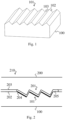
- the present invention relates to the field of the arrangement of microstructures of optical guides used to extract virtual images injected and transported in these optical guides.
Landscapes
- Physics & Mathematics (AREA)
- General Physics & Mathematics (AREA)
- Optics & Photonics (AREA)
- Engineering & Computer Science (AREA)
- Manufacturing & Machinery (AREA)
- Optical Elements Other Than Lenses (AREA)
- Optical Couplings Of Light Guides (AREA)
Claims (12)
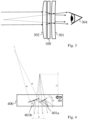
- Optischer Leiter (400, 800), der ein erstes Teil (800a) aus einem transparenten Material beinhaltet, wobei das erste Teil an der Oberfläche ein Netzwerk aus Extraktionsmikrostrukturen aufweist, das aus einer Aufeinanderfolge von Extraktionsmikrostrukturen zusammengesetzt ist, die dafür angeordnet sind, in einem endlichen Abstand D ein virtuelles Bild zu projizieren, das in den optischen Leiter injiziert wird, wobei jede Extraktionsmikrostruktur eine zweiseitige Prismenform aufweist, wobei eine Seite aktive Fläche (401a, 401b, 801a, 801b) genannt wird und über eine halbreflektierende Ablagerung verfügt, um das virtuelle Bild aus dem optischen Leiter zu extrahieren, und die andere Seite passive Fläche genannt wird und über keine halbreflektierende Ablagerung verfügt, dadurch gekennzeichnet, dass jede aktive Fläche sphärisch ist und eine Neigung aufweist, die um einen durchschnittlichen Winkel θ geringer ist als die eventuelle aktive Fläche, die in der Aufeinanderfolge von Extraktionsmikrostrukturen in der Ausbreitungsrichtung des virtuellen Bildes im optischen Leiter unmittelbar vorangeht, dadurch gekennzeichnet, dass:


- Optischer Leiter nach Anspruch 1, der ferner ein zweites Teil (800b), Abdeckteil genannt, aus dem gleichen transparenten Material wie das erste Teil beinhaltet, wobei das zweite Teil Mikrostrukturen beinhaltet, die dafür angeordnet sind, in Räumen zwischen den Mikrostrukturen des ersten Teils Platz zu finden, wobei das zweite Teil so an das erste Teil geklebt ist, dass ein optischer Leiter mit zwei parallelen Seiten gebildet wird.
- Optischer Leiter nach Anspruch 2, wobei das zweite Teil an der Oberfläche Mikrostrukturen mit Formen aufweist, die zu jenen der Mikrostrukturen des ersten Teils komplementär sind, mit einer im Wesentlichen konstanten Klebstoffdicke.
- Optischer Leiter nach Anspruch 2, wobei das zweite Teil an der Oberfläche Mikrostrukturen aufweist, die ein anderes Netzwerk aus Extraktionsmikrostrukturen bilden, das eine andere Aufeinanderfolge von Extraktionsmikrostrukturen mit aktiven Flächen (802a, 802b) beinhaltet, die über eine halbreflektierende Ablagerung verfügen und die dafür angeordnet sind, das virtuelle Bild in einem Abstand D' zu projizieren, der sich von dem Abstand D unterscheidet.
- Optischer Leiter nach Anspruch 4, wobei der Abstand D' endlich ist und jede aktive Fläche der Mikrostrukturen dieses anderen Netzwerks aus Extraktionsmikrostrukturen sphärisch ist und eine Neigung aufweist, die um einen durchschnittlichen Winkel θ' geringer ist als die eventuelle aktive Fläche, die in der Aufeinanderfolge von Extraktionsmikrostrukturen in der Ausbreitungsrichtung des virtuellen Bildes im optischen Leiter unmittelbar vorangeht.
- Optischer Leiter nach Anspruch 4, wobei der Abstand D' unendlich ist.
- Optischer Leiter nach einem der Ansprüche 4 bis 6, wobei- die halbreflektierende Ablagerung der aktiven Flächen des ersten Teils auf eine spezifische Polarisation anspricht und die halbreflektierende Ablagerung der aktiven Flächen des zweiten Teils auf eine andere spezifische Polarisation anspricht; oder- die halbreflektierende Ablagerung der aktiven Flächen des ersten Teils auf eine spezifische Wellenlänge anspricht und die halbreflektierende Ablagerung der aktiven Flächen des zweiten Teils auf eine andere spezifische Wellenlänge anspricht; oder- die halbreflektierende Ablagerung der aktiven Flächen des ersten Teils auf ein spezifisches Spektralband anspricht und die halbreflektierende Ablagerung der aktiven Flächen des zweiten Teils auf ein anderes spezifisches Spektralband anspricht.
- Bildprojektionsvorrichtung, die einen optischen Leiter nach einem der Ansprüche 1 bis 7 und eine Kollimationsvorrichtung, die ein auf unendlich kollimiertes virtuelles Bild bereitstellt, beinhaltet, wobei die Kollimationsvorrichtung und der optische Leiter so zusammengesetzt sind, dass das virtuelle Bild, das von der Kollimationsvorrichtung bereitgestellt wird, in den optischen Leiter injiziert und im Abstand D von dem Netzwerk aus Extraktionsmikrostrukturen projiziert wird.
- System für erweiterte Realität, das wenigstens eine Bildprojektionsvorrichtung nach Anspruch 8 beinhaltet.
- Verfahren zur Herstellung eines optischen Leiters, das die folgenden Schritte beinhaltet- Herstellen eines ersten Teils aus einem transparenten Material, wobei das erste Teil an der Oberfläche ein Netzwerk aus Extraktionsmikrostrukturen aufweist, das aus einer Aufeinanderfolge von Extraktionsmikrostrukturen zusammengesetzt ist, die dafür angeordnet sind, in einem endlichen Abstand D ein virtuelles Bild zu projizieren, das in den optischen Leiter injiziert wird, wobei jede Extraktionsmikrostruktur eine zweiseitige Prismenform aufweist, wobei eine Seite aktive Fläche genannt wird, um das virtuelle Bild aus dem optischen Leiter zu extrahieren, und die andere Seite passive Fläche genannt wird, wobei jede aktive Fläche sphärisch ist und eine Neigung aufweist, die um einen durchschnittlichen Winkel θ geringer ist als die eventuelle aktive Fläche, die in der Aufeinanderfolge von Extraktionsmikrostrukturen in der Ausbreitungsrichtung des virtuellen Bildes im optischen Leiter unmittelbar vorangeht,- Anwenden einer halbreflektierenden Behandlung auf die aktiven Flächen unter Ausschluss der passiven Flächen;
dadurch gekennzeichnet, dass das Herstellungsverfahren so geartet ist, dass:

- Herstellungsverfahren nach Anspruch 10, wobei das erste Teil ferner an der Oberfläche ein Netzwerk aus Mikrostrukturen zur zweidimensionalen Pupillenvervielfältigung beinhaltet, das zwischen einem Injektionsbereich, durch welchen das zu projizierende virtuelle Bild in den optischen Leiter injiziert wird, und dem Netzwerk aus Extraktionsmikrostrukturen platziert ist, wobei die Mikrostrukturen zur zweidimensionalen Pupillenvervielfältigung aktive Flächen in Form von geneigten Ebenen beinhalten und die anderen Flächen passive Flächen sind, wobei die Mikrostrukturen zur zweidimensionalen Pupillenvervielfältigung schräg im Verhältnis zu den Extraktionsmikrostrukturen platziert sind, um einen Lichtstrahl des transportierten virtuellen Bildes, der auf eine oder mehrere ihrer aktiven Flächen trifft, in Richtung des Netzwerks aus Extraktionsmikrostrukturen zu reflektieren,
und das Verfahren ferner den folgenden Schritt beinhaltet- Anwenden einer halbreflektierenden Behandlung auf die aktiven Flächen der Mikrostrukturen zur zweidimensionalen Pupillenvervielfältigung, unter Ausschluss der passiven Flächen. - Herstellungsverfahren nach Anspruch 10 oder 11, das ferner die folgenden Schritte beinhaltet- Herstellen eines zweiten Teils, Abdeckteil genannt, aus dem gleichen transparenten Material wie das erste Teil, wobei das zweite Teil Mikrostrukturen beinhaltet, die dafür angeordnet sind, in Räumen zwischen den Mikrostrukturen des ersten Teils Platz zu finden,- Verkleben des ersten Teils und des zweiten Teils, um einen optischen Leiter mit zwei parallelen Seiten zu bilden.
Applications Claiming Priority (1)
| Application Number | Priority Date | Filing Date | Title |
|---|---|---|---|
| FR2103209A FR3121236B1 (fr) | 2021-03-29 | 2021-03-29 | Guide optique et procede de fabrication correspondant |
Publications (3)
| Publication Number | Publication Date |
|---|---|
| EP4067950A1 EP4067950A1 (de) | 2022-10-05 |
| EP4067950B1 true EP4067950B1 (de) | 2025-07-02 |
| EP4067950C0 EP4067950C0 (de) | 2025-07-02 |
Family
ID=77913144
Family Applications (1)
| Application Number | Title | Priority Date | Filing Date |
|---|---|---|---|
| EP22164658.1A Active EP4067950B1 (de) | 2021-03-29 | 2022-03-28 | Lichtwellenleiter und entsprechendes herstellungsverfahren |
Country Status (3)
| Country | Link |
|---|---|
| US (2) | US12019241B2 (de) |
| EP (1) | EP4067950B1 (de) |
| FR (1) | FR3121236B1 (de) |
Families Citing this family (3)
| Publication number | Priority date | Publication date | Assignee | Title |
|---|---|---|---|---|
| CN115335749A (zh) * | 2020-06-27 | 2022-11-11 | 鲁姆斯有限公司 | 车辆平视显示器(hud) |
| CN115373064A (zh) * | 2021-05-20 | 2022-11-22 | 中强光电股份有限公司 | 光波导 |
| CN120077318A (zh) * | 2022-11-04 | 2025-05-30 | 谷歌有限责任公司 | 单光导结构中的二维光瞳扩展 |
Family Cites Families (35)
| Publication number | Priority date | Publication date | Assignee | Title |
|---|---|---|---|---|
| US1069848A (en) * | 1910-03-21 | 1913-08-12 | Brown Bag Filling Machine Company | Bag-filling machine. |
| US4220400A (en) * | 1977-02-22 | 1980-09-02 | Honeywell Inc. | Display apparatus with reflective separated structure |
| GB9314991D0 (en) * | 1993-07-20 | 1993-09-01 | Sandoz Ltd | Mechanical device |
| US6395558B1 (en) * | 1996-08-29 | 2002-05-28 | Zeptosens Ag | Optical chemical/biochemical sensor |
| EP1443320A3 (de) * | 1997-09-10 | 2005-02-02 | Artificial Sensing Instruments ASI AG | Sensorchip zur Charakterisierung einer chemischen und/oder biochemischen Substanz |
| EP2189783A1 (de) * | 2000-08-09 | 2010-05-26 | Artificial Sensing Instruments ASI AG | Wellenleitergitterstruktur und optische Messanordnung |
| DE10124370B4 (de) * | 2001-05-18 | 2010-11-18 | Zumtobel Lighting Gmbh | Optisches Element mit Totalreflexion |
| JP2005249882A (ja) * | 2004-03-01 | 2005-09-15 | Miyakawa:Kk | 液晶表示装置 |
| JP4149978B2 (ja) * | 2004-09-16 | 2008-09-17 | 株式会社東芝 | フレネルレンズおよび照明装置 |
| US7206107B2 (en) * | 2004-12-13 | 2007-04-17 | Nokia Corporation | Method and system for beam expansion in a display device |
| CN101512413B (zh) * | 2006-09-28 | 2012-02-15 | 诺基亚公司 | 利用三维衍射元件的光束扩展 |
| US20090255568A1 (en) * | 2007-05-01 | 2009-10-15 | Morgan Solar Inc. | Solar panel window |
| FR2925171B1 (fr) | 2007-12-13 | 2010-04-16 | Optinvent | Guide optique et systeme optique de vision oculaire |
| EP2370854B1 (de) * | 2008-12-18 | 2016-09-28 | 3M Innovative Properties Company | Lichtleiter mit erhöhter lichtextraktion |
| DE102009010537B4 (de) * | 2009-02-25 | 2018-03-01 | Carl Zeiss Smart Optics Gmbh | Strahlvereiniger und Verwendung eines solchen in einer Anzeigevorrichtung |
| US20120062991A1 (en) * | 2009-05-28 | 2012-03-15 | Koninklijke Philips Electronics N.V. | Autostereoscopic display device |
| KR101822672B1 (ko) * | 2010-01-13 | 2018-01-26 | 쓰리엠 이노베이티브 프로퍼티즈 컴파니 | 점탄성 도광체를 구비한 조명 장치 |
| FR2973889B1 (fr) | 2011-04-05 | 2014-01-03 | Optinvent | Dispositif de guidage optique et procede de fabrication d'un tel dispositif |
| FR2983976B1 (fr) | 2011-12-13 | 2017-10-20 | Optinvent | Guide optique a elements de guidage superposes et procede de fabrication |
| US8384999B1 (en) * | 2012-01-09 | 2013-02-26 | Cerr Limited | Optical modules |
| US8665178B1 (en) | 2012-03-01 | 2014-03-04 | Google, Inc. | Partially-reflective waveguide stack and heads-up display using same |
| DE102013219622B4 (de) * | 2013-09-27 | 2021-01-14 | tooz technologies GmbH | Optisches Element und Anzeigevorrichtung mit einem solchen optischen Element |
| US9835866B2 (en) * | 2013-09-27 | 2017-12-05 | Carl Zeiss Smart Optics Gmbh | Spectacle lens for a display device that can be fitted on the head of a user and generates an image |
| CN105940509A (zh) * | 2014-02-28 | 2016-09-14 | 松下知识产权经营株式会社 | 发光装置 |
| JP6337145B2 (ja) * | 2014-12-10 | 2018-06-06 | シャープ株式会社 | 照明装置及び表示装置 |
| US10732344B2 (en) * | 2015-08-26 | 2020-08-04 | 3M Innovative Properties Company | Collimating light guide |
| CN108292007A (zh) * | 2015-09-10 | 2018-07-17 | 巴尔·姆昆德·达尔 | 导光装置及其制造方法 |
| WO2017094493A1 (ja) * | 2015-12-03 | 2017-06-08 | シャープ株式会社 | 導光板、ライトガイドおよび虚像表示装置 |
| CN112524500B (zh) * | 2016-02-22 | 2023-07-28 | 亮锐控股有限公司 | 来自照明设备的不对称光强分布 |
| JP7046953B2 (ja) * | 2016-12-29 | 2022-04-04 | コーニング インコーポレイテッド | 微細構造およびパターンが施された導光板、および、それを用いた装置 |
| JP6662333B2 (ja) * | 2017-03-14 | 2020-03-11 | オムロン株式会社 | 表示装置 |
| US9927586B1 (en) * | 2017-03-20 | 2018-03-27 | Sae Magnetics (H.K.) Ltd. | Two-part optical coupling subassembly for monitoring optical output power in optical transceiver |
| TWI759451B (zh) * | 2017-03-31 | 2022-04-01 | 日商巴川製紙所股份有限公司 | 使用各向異性光學膜之導光積層體及使用該導光積層體的面狀光源裝置 |
| KR102753311B1 (ko) | 2017-05-16 | 2025-01-10 | 매직 립, 인코포레이티드 | 혼합 현실을 위한 시스템들 및 방법들 |
| WO2019136476A1 (en) * | 2018-01-08 | 2019-07-11 | Digilens, Inc. | Waveguide architectures and related methods of manufacturing |
-
2021
- 2021-03-29 FR FR2103209A patent/FR3121236B1/fr active Active
- 2021-11-19 US US17/531,082 patent/US12019241B2/en active Active
-
2022
- 2022-03-25 US US17/704,633 patent/US20220308279A1/en active Pending
- 2022-03-28 EP EP22164658.1A patent/EP4067950B1/de active Active
Also Published As
| Publication number | Publication date |
|---|---|
| FR3121236B1 (fr) | 2024-02-09 |
| FR3121236A1 (fr) | 2022-09-30 |
| US12019241B2 (en) | 2024-06-25 |
| US20220308350A1 (en) | 2022-09-29 |
| EP4067950A1 (de) | 2022-10-05 |
| EP4067950C0 (de) | 2025-07-02 |
| US20220308279A1 (en) | 2022-09-29 |
Similar Documents
| Publication | Publication Date | Title |
|---|---|---|
| EP2695017B1 (de) | Vorrichtung zur optischen wellenleitung und verfahren zur herstellung einer solchen vorrichtung | |
| EP4067950B1 (de) | Lichtwellenleiter und entsprechendes herstellungsverfahren | |
| EP2791717B1 (de) | Wellenleiter mit übereinanderliegenden leitelementen und herstellungsverfahren dafür | |
| EP1792224B1 (de) | Verfahren zur herstellung einer ophthalmischen linse für die herstellung einer optischen anzeige | |
| EP3610309B1 (de) | Photonischer chip mit integrierter kollimationsstruktur | |
| EP2220523B1 (de) | Optischer leiter und optisches system für sehkraft | |
| EP3063468B1 (de) | Optischer leiter zur erzeugung zwei leuchtender prägungen | |
| EP3074809B1 (de) | Vorrichtung zur erweiterung der austrittspupille und scheinwerferanzeige mit dieser vorrichtung | |
| EP2277074B1 (de) | Informative brille | |
| FR2999301A1 (fr) | Guide optique d'images collimatees a dedoubleur de faisceaux optiques et dispositif optique associe | |
| FR2948775A1 (fr) | Systeme optique planaire d'imagerie polychromatique a large champ de vision | |
| EP3203316B1 (de) | Anzeigesystem eines bildes auf einer windschutzscheibe | |
| EP3404457A1 (de) | Photonen-chip mit reflektierender struktur zur rückfaltung des lichtwegs | |
| JP2012009300A (ja) | 導光板の製造方法及び導光板 | |
| JP2015179297A (ja) | 導光板の製造方法及び導光板 | |
| FR3064123A1 (fr) | Dispositif lumineux avec moyen mobile de balayage et fibre optique | |
| FR2925172A1 (fr) | Guide optique et systeme optique de vision oculaire. | |
| FR3110978A1 (fr) | Dispositif de répartition de lumière basé sur un guide d’onde planaire | |
| EP3525015A1 (de) | Optisches monoblockelement mit diaphragma | |
| WO2011058156A1 (fr) | Dispositif de visualisation d'images superposées à une image d'une scène environnante, et procédé de fabrication associé | |
| FR2888341A1 (fr) | Dispositif de commutation optique ameliore | |
| FR2855274A1 (fr) | Circuit integre photonique equipe de moyens d'interconnexion avec des composants optoelectroniques rapportes | |
| FR3034878A1 (fr) | Systeme d'affichage d'une image flottante | |
| FR3004816A1 (fr) | Generateur d'images pour afficheur, notamment afficheur tete haute |
Legal Events
| Date | Code | Title | Description |
|---|---|---|---|
| PUAI | Public reference made under article 153(3) epc to a published international application that has entered the european phase |
Free format text: ORIGINAL CODE: 0009012 |
|
| STAA | Information on the status of an ep patent application or granted ep patent |
Free format text: STATUS: THE APPLICATION HAS BEEN PUBLISHED |
|
| AK | Designated contracting states |
Kind code of ref document: A1 Designated state(s): AL AT BE BG CH CY CZ DE DK EE ES FI FR GB GR HR HU IE IS IT LI LT LU LV MC MK MT NL NO PL PT RO RS SE SI SK SM TR |
|
| STAA | Information on the status of an ep patent application or granted ep patent |
Free format text: STATUS: REQUEST FOR EXAMINATION WAS MADE |
|
| 17P | Request for examination filed |
Effective date: 20230405 |
|
| RBV | Designated contracting states (corrected) |
Designated state(s): AL AT BE BG CH CY CZ DE DK EE ES FI FR GB GR HR HU IE IS IT LI LT LU LV MC MK MT NL NO PL PT RO RS SE SI SK SM TR |
|
| STAA | Information on the status of an ep patent application or granted ep patent |
Free format text: STATUS: EXAMINATION IS IN PROGRESS |
|
| 17Q | First examination report despatched |
Effective date: 20240724 |
|
| GRAP | Despatch of communication of intention to grant a patent |
Free format text: ORIGINAL CODE: EPIDOSNIGR1 |
|
| STAA | Information on the status of an ep patent application or granted ep patent |
Free format text: STATUS: GRANT OF PATENT IS INTENDED |
|
| INTG | Intention to grant announced |
Effective date: 20250203 |
|
| GRAS | Grant fee paid |
Free format text: ORIGINAL CODE: EPIDOSNIGR3 |
|
| GRAA | (expected) grant |
Free format text: ORIGINAL CODE: 0009210 |
|
| STAA | Information on the status of an ep patent application or granted ep patent |
Free format text: STATUS: THE PATENT HAS BEEN GRANTED |
|
| AK | Designated contracting states |
Kind code of ref document: B1 Designated state(s): AL AT BE BG CH CY CZ DE DK EE ES FI FR GB GR HR HU IE IS IT LI LT LU LV MC MK MT NL NO PL PT RO RS SE SI SK SM TR |
|
| REG | Reference to a national code |
Ref country code: GB Ref legal event code: FG4D Free format text: NOT ENGLISH |
|
| REG | Reference to a national code |
Ref country code: CH Ref legal event code: EP |
|
| REG | Reference to a national code |
Ref country code: DE Ref legal event code: R096 Ref document number: 602022016679 Country of ref document: DE |
|
| REG | Reference to a national code |
Ref country code: IE Ref legal event code: FG4D Free format text: LANGUAGE OF EP DOCUMENT: FRENCH |
|
| U01 | Request for unitary effect filed |
Effective date: 20250730 |
|
| U07 | Unitary effect registered |
Designated state(s): AT BE BG DE DK EE FI FR IT LT LU LV MT NL PT RO SE SI Effective date: 20250807 |