EP4066321B1 - Buchsenkontakt mit seitlichem kabelabgang - Google Patents
Buchsenkontakt mit seitlichem kabelabgang Download PDFInfo
- Publication number
- EP4066321B1 EP4066321B1 EP20833719.6A EP20833719A EP4066321B1 EP 4066321 B1 EP4066321 B1 EP 4066321B1 EP 20833719 A EP20833719 A EP 20833719A EP 4066321 B1 EP4066321 B1 EP 4066321B1
- Authority
- EP
- European Patent Office
- Prior art keywords
- contact element
- contact
- electrical contact
- opening
- recess
- Prior art date
- Legal status (The legal status is an assumption and is not a legal conclusion. Google has not performed a legal analysis and makes no representation as to the accuracy of the status listed.)
- Active
Links
Images

Classifications
-
- H—ELECTRICITY
- H01—ELECTRIC ELEMENTS
- H01R—ELECTRICALLY-CONDUCTIVE CONNECTIONS; STRUCTURAL ASSOCIATIONS OF A PLURALITY OF MUTUALLY-INSULATED ELECTRICAL CONNECTING ELEMENTS; COUPLING DEVICES; CURRENT COLLECTORS
- H01R11/00—Individual connecting elements providing two or more spaced connecting locations for conductive members which are, or may be, thereby interconnected, e.g. end pieces for wires or cables supported by the wire or cable and having means for facilitating electrical connection to some other wire, terminal, or conductive member, blocks of binding posts
- H01R11/11—End pieces or tapping pieces for wires, supported by the wire and for facilitating electrical connection to some other wire, terminal or conductive member
- H01R11/28—End pieces consisting of a ferrule or sleeve
-
- H—ELECTRICITY
- H01—ELECTRIC ELEMENTS
- H01R—ELECTRICALLY-CONDUCTIVE CONNECTIONS; STRUCTURAL ASSOCIATIONS OF A PLURALITY OF MUTUALLY-INSULATED ELECTRICAL CONNECTING ELEMENTS; COUPLING DEVICES; CURRENT COLLECTORS
- H01R13/00—Details of coupling devices of the kinds covered by groups H01R12/70 or H01R24/00 - H01R33/00
- H01R13/02—Contact members
- H01R13/15—Pins, blades or sockets having separate spring member for producing or increasing contact pressure
- H01R13/187—Pins, blades or sockets having separate spring member for producing or increasing contact pressure with spring member in the socket
-
- H—ELECTRICITY
- H01—ELECTRIC ELEMENTS
- H01R—ELECTRICALLY-CONDUCTIVE CONNECTIONS; STRUCTURAL ASSOCIATIONS OF A PLURALITY OF MUTUALLY-INSULATED ELECTRICAL CONNECTING ELEMENTS; COUPLING DEVICES; CURRENT COLLECTORS
- H01R25/00—Coupling parts adapted for simultaneous co-operation with two or more identical counterparts, e.g. for distributing energy to two or more circuits
-
- H—ELECTRICITY
- H01—ELECTRIC ELEMENTS
- H01R—ELECTRICALLY-CONDUCTIVE CONNECTIONS; STRUCTURAL ASSOCIATIONS OF A PLURALITY OF MUTUALLY-INSULATED ELECTRICAL CONNECTING ELEMENTS; COUPLING DEVICES; CURRENT COLLECTORS
- H01R9/00—Structural associations of a plurality of mutually-insulated electrical connecting elements, e.g. terminal strips or terminal blocks; Terminals or binding posts mounted upon a base or in a case; Bases therefor
- H01R9/22—Bases, e.g. strip, block, panel
- H01R9/24—Terminal blocks
- H01R9/2408—Modular blocks
-
- H—ELECTRICITY
- H01—ELECTRIC ELEMENTS
- H01R—ELECTRICALLY-CONDUCTIVE CONNECTIONS; STRUCTURAL ASSOCIATIONS OF A PLURALITY OF MUTUALLY-INSULATED ELECTRICAL CONNECTING ELEMENTS; COUPLING DEVICES; CURRENT COLLECTORS
- H01R13/00—Details of coupling devices of the kinds covered by groups H01R12/70 or H01R24/00 - H01R33/00
- H01R13/02—Contact members
- H01R13/10—Sockets for co-operation with pins or blades
- H01R13/11—Resilient sockets
- H01R13/111—Resilient sockets co-operating with pins having a circular transverse section
-
- H—ELECTRICITY
- H01—ELECTRIC ELEMENTS
- H01R—ELECTRICALLY-CONDUCTIVE CONNECTIONS; STRUCTURAL ASSOCIATIONS OF A PLURALITY OF MUTUALLY-INSULATED ELECTRICAL CONNECTING ELEMENTS; COUPLING DEVICES; CURRENT COLLECTORS
- H01R4/00—Electrically-conductive connections between two or more conductive members in direct contact, i.e. touching one another; Means for effecting or maintaining such contact; Electrically-conductive connections having two or more spaced connecting locations for conductors and using contact members penetrating insulation
- H01R4/10—Electrically-conductive connections between two or more conductive members in direct contact, i.e. touching one another; Means for effecting or maintaining such contact; Electrically-conductive connections having two or more spaced connecting locations for conductors and using contact members penetrating insulation effected solely by twisting, wrapping, bending, crimping, or other permanent deformation
- H01R4/18—Electrically-conductive connections between two or more conductive members in direct contact, i.e. touching one another; Means for effecting or maintaining such contact; Electrically-conductive connections having two or more spaced connecting locations for conductors and using contact members penetrating insulation effected solely by twisting, wrapping, bending, crimping, or other permanent deformation by crimping
- H01R4/183—Electrically-conductive connections between two or more conductive members in direct contact, i.e. touching one another; Means for effecting or maintaining such contact; Electrically-conductive connections having two or more spaced connecting locations for conductors and using contact members penetrating insulation effected solely by twisting, wrapping, bending, crimping, or other permanent deformation by crimping for cylindrical elongated bodies, e.g. cables having circular cross-section
Definitions
- the invention is based on an electrical contact element according to the preamble of independent claim 1.
- Such contact elements are used in particular in the railway industry to transmit high currents. Such a contact element is often exposed to a current of a thousand amperes or more.
- the EP 2 569 825 B1 shows a contact element that can be designed as a socket or pin contact. With a socket contact, the opening in the connection area and the opening in the contact area run parallel. The contact blades of the socket contact define the contact points with a matching pin contact. This means that each socket contact can be electrically connected to exactly one pin contact.
- the EP 2 061 119 A2 shows an electrical contact element comprising a cylindrical socket contact and a contact holder, which is connected to the socket contact in a force- and form-fitting manner.
- the FR 2 932 613 A1 shows a contact pin and a matching socket plug connected to one end of an electrical cable.
- the US 2014/120760 A1 shows a device comprising a first electrical connector with a first housing, a contact element with a first portion connected to the first housing, and a first elastic element for supporting the first portion in the first housing.
- the first elastic element is deflectable to enable movement of the contact element relative to the first housing.
- German Patent and Trademark Office has searched the following prior art in the priority application for the present application: FR 2 932 613 A1 , DE 20 2004 005 593 U1 , CN 206 585 111 U and US 2003/0068931 A1 .
- the contact strip is advantageously made of a material that contains beryllium. Such a material ensures a reliable current bridge between the contact pin and the contact socket. Alloys such as beryllium copper or copper beryllium are particularly preferred.
- the contact area of the contact element has a plug-in side and an exit side.
- a recess is made in the plug-in side and the exit side is provided with a raised portion.
- the recess and the raised portion are designed to complement each other. This means that several contact elements according to the invention can be lined up in a form-fitting manner.
- the electrical contact element is rotationally symmetrical with respect to its axis of symmetry SA.
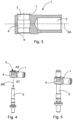
- the contact element 1 has a connection area A and a contact area K.
- the connection area A has a cylindrical opening 2 and the contact area has a cylindrical through-opening 3.
- the opening 2 and the through-opening 3 or their main axes of symmetry extend orthogonally to one another.
- a circumferential contact band 4 is arranged approximately centrally within the cylindrical through-opening 3, which is slightly enlarged in Figure 2 is shown.
- the contact element 1 is guided in the plugging direction SR to the counter contact element 5, as in Figure 4 can be seen.
- the contact strip 4 has a grid-like basic structure that is joined together to form a ring.
- the contact strip 4 defines the electrical contact points that a matching mating contact element 5, in this case a contact pin, forms with the contact element 1, in this case a socket contact.
- the contact strip 4 preferably consists of a beryllium-containing material.
- the contact element 1 is transparent in order to be able to see the contact strip 4 arranged in the contact area K. to be able to see.
- Figure 5 It can be seen that when plugged in, the contact strip 4 touches the pin contact 5 that penetrates the through hole 3. The contact strip 4 therefore forms a contact bridge between the socket contact 1 and the pin contact 5.
- the contact area K of the contact element 1 has a plug-in side ST and an exit side AS opposite it.
- a recess 6 is provided on the plug-in side ST and the exit side AS has a raised portion 7 which is designed to be complementary to the recess 6.
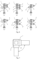
- the recess 6 and the raised portion 7 have a substantially rectangular cross-section. This allows the openings 2, 2', 2" in the connection areas A of different but similar contact elements 1, 1', 1" to form an angle ( ⁇ ) with one another. This angular position is in Figure 7 shown schematically.
- the angle ( ⁇ ) can be equal to 90° or a multiple of 90°. With other cross-sectional geometries, other angular positions can be achieved accordingly. Different alignments between contact elements 1, 1', 1" arranged in a row are shown in Figure 6 shown.
Landscapes
- Connector Housings Or Holding Contact Members (AREA)
- Connections Effected By Soldering, Adhesion, Or Permanent Deformation (AREA)
- Multi-Conductor Connections (AREA)
Description
- Die Erfindung geht aus von einem elektrischen Kontaktelement nach der Gattung des unabhängigen Anspruchs 1.
- Derartige Kontaktelemente werden insbesondere in der Bahnindustrie zur Übertragung hoher Ströme eingesetzt. Oftmals wird ein derartiges Kontaktelement einer Stromstärke von tausend Ampere und mehr ausgesetzt.
- Die
EP 2 569 825 B1 zeigt ein Kontaktelement, welches als Buchsen- oder als Stiftkontakt ausgeführt sein kann. Beim Buchsenkontakt verlaufen die Öffnung im Anschlussbereich und die Öffnung im Kontaktbereich parallel. Die Kontaktlamellen des Buchsenkontakts definieren die Kontaktpunkte mit einem passenden Stiftkontakt. Dadurch kann jeder Buchsenkontakt mit genau einem Stiftkontakt elektrisch leitend kontaktiert werden. - Die
EP 2 061 119 A2 zeigt ein elektrisches Kontaktelement umfassend einen zylinderförmigen Buchsenkontakt und einen Kontakthalter, welcher mit dem Buchsenkontakt kraft- und formschlüssig verbunden ist. - Die
FR 2 932 613 A1 - Die
US 2014/120760 A1 zeigt eine Vorrichtung umfasst einen ersten elektrischen Verbinder mit einem ersten Gehäuse, einem Kontaktelement mit einem ersten Abschnitt, der mit dem ersten Gehäuse verbunden ist, und einem ersten elastischen Element zum Stützen des ersten Abschnitts in dem ersten Gehäuse. Das erste elastische Element ist auslenkbar, um eine Bewegung des Kontaktelements relativ zum ersten Gehäuse zu ermöglichen. - Das Deutsche Patent- und Markenamt hat in der Prioritätsanmeldung zu vorliegender Anmeldung den folgenden Stand der Technik recherchiert:
FR 2 932 613 A1 DE 20 2004 005 593 U1 ,CN 206 585 111 U undUS 2003/0068931 A1 . - Die Aufgabe der Erfindung besteht darin ein leistungsfähiges elektrisches Kontaktelement bereitzustellen, welches außerdem in kompakten Einbausituationen einsetzbar ist.
- Die Aufgabe wird durch den Gegenstand der unabhängigen Ansprüche gelöst.
- Vorteilhafte Ausgestaltungen der Erfindung sind in den Unteransprüchen und der folgenden Beschreibung angegeben.
- Das erfindungsgemäße elektrische Kontaktelement ist zur Übertragung hoher Ströme vorgesehen. Hierbei treten oftmals Stromstärken von tausend Ampere und mehr auf.
- Das elektrische Kontaktelement weist einen Anschlussbereich und einen Kontaktbereich auf. Der Anschlussbereich weist eine zylinderförmige Öffnung auf und bildet vorteilhafterweise einen Crimpanschluss auf. Der Kontaktbereich weist eine zylinderförmige Durchgangsöffnung auf. Der Kontaktbereich weist eine Steckseite auf, auf welcher ein passender Kontaktstift eines Stiftkontaktelements in die Durchgangsöffnung eingeführt wird. Der Kontaktbereich weist auf der gegenüberliegenden Seite der Steckseite eine Austrittsseite auf, aus welcher der Kontaktstift des Stiftkontaktelements wieder heraustritt.
- Die Öffnung des Anschluss- bzw. Crimpbereichs und die Durchgangsöffnung des Kontaktbereichs erstrecken sich orthogonal zueinander. Das bedeutet, dass sich die verlängerten Richtungsvektoren der Öffnungen orthogonal schneiden.
- Ein flächiger Kontakt zwischen dem Buchsenkontakt und einem dazu passenden Stiftkontakt hätte eine starke Erwärmung der Steckverbindung zur Folge. Innerhalb der zylinderförmigen Durchgangsöffnung ist daher ein umlaufendes Kontaktband angeordnet. Über das Kontaktband werden konkrete Kontaktpunkte zwischen dem erfindungsgemäßen Buchsenkontakt und Stiftkontakt definiert. Dadurch wird der Übergangswiderstand der Steckverbindung reduziert.
- Das Kontaktband erstreckt sich nicht innerhalb der gesamten Durchgangsöffnung. Vorteilhafterweise ist das umlaufendes Kontaktband etwa mittig in der zylinderförmigen Durchgangsöffnung des Anschlussbereichs angeordnet. Dadurch wird ein so genanntes Kippeln des Kontaktstiftes weitestgehend verhindert.
- Vorteilhafterweise besteht das Kontaktband aus einem Material, welches Beryllium enthält. Ein solches Material sorgt für eine zuverlässige Strombrücke zwischen Kontaktstift und Kontaktbuchse. Besonders bevorzugt sind hierbei Legierungen wie Berylliumkupfer oder Kupferberyllium.
- Wie bereits oben erwähnt, weist der Kontaktbereich des Kontaktelements eine Steckseite und eine Austrittsseite auf. Vorzugsweise ist in die Steckseite eine Aussparung eingebracht und die Austrittsseite ist mit einer Erhebung versehen. Die Aussparung und die Erhebung sind komplementär zueinander ausgebildet. Dadurch können mehrere erfindungsgemäße Kontaktelemente formschlüssig aneinandergereiht werden.
- In einer besonders vorteilhaften Ausführungsform der Erfindung weisen die Aussparung und die Erhebung des Kontaktbereichs einen im Wesentlichen rechteckigen Querschnitt auf. Dadurch können die Kontaktelemente um 90°, oder ein Vielfaches davon, versetzt zueinander aneinandergereiht werden.
- Vorzugsweise besteht das elektrische Kontaktelement im Wesentlichen aus Kupfer. Dadurch wird eine gute elektrische Leitfähigkeit, insbesondere gegenüber anderen Materialien, wie beispielsweise Messing, gewährleistet. Die Oberfläche des Kupferbasiskörpers des Kontaktelements ist mit einer Silber- oder Silberlegierungsschicht überzogen. Dadurch wird die Stromtragfähigkeit des Kontaktelements nochmals deutlich erhöht.
- Vorteilhafterweise ist das elektrische Kontaktelement rotationssymmetrisch. Dadurch kann das Kontaktelement einfach aus Vollmaterial in einem zerspanenden Arbeitsgang hergestellt werden.
- Ein Ausführungsbeispiel der Erfindung ist in den Zeichnungen dargestellt und wird im Folgenden näher erläutert. Es zeigen:
- Fig. 1
- eine perspektivische Darstellung eines erfindungsgemäßen Kontaktelements,
- Fig. 2
- eine perspektivische Darstellung eines Kontaktbandes,
- Fig. 3
- eine Schnittdarstellung des erfindungsgemäßen Kontaktelements,
- Fig. 4
- eine perspektivische Darstellung eines erfindungsgemäßen Kontaktelements und eines dazu passenden Gegenkontaktelements (Stiftkontakt),
- Fig. 5
- eine perspektivische Darstellung des mit dem Gegenkontaktelement gesteckten erfindungsgemäßen Kontaktelements,
- Fig. 6
- eine perspektivische Darstellung verschiedener kombinatorischer Varianten mehrerer erfindungsgemäßer Kontaktelemente, die zusammen mit einem Gegenkontaktelement elektrisch leitend verbunden sind und
- Fig. 7
- eine schematische Draufsicht zweier miteinander zusammengefügter Kontaktelemente.
- Die Figuren enthalten teilweise vereinfachte, schematische Darstellungen. Zum Teil werden für gleiche, aber gegebenenfalls nicht identische Elemente identische Bezugszeichen verwendet. Verschiedene Ansichten gleicher Elemente könnten unterschiedlich skaliert sein.
- Richtungsangaben wie beispielsweise "links", "rechts", "oben" und "unten" sind mit Bezug auf die jeweilige Figur zu verstehen und können in den einzelnen Darstellungen gegenüber dem dargestellten Objekt variieren.
- Die
Figur 1 zeigt eine mögliche Ausgestaltung eines erfindungsgemäßen Kontaktelements 1. Das Kontaktelement 1 ist massiv ausgestaltet und beispielsweise aus einem massiven Kupferwerkstück in einem spanenden Arbeitsgang herausgearbeitet. Daher ist das Kontaktelement 1 besonders zur Übertragung hoher Ströme geeignet. - Das elektrische Kontaktelement rotationssymmetrisch bzgl. seiner Symmetrieachse SA ausgebildet. Das Kontaktelement 1 weist einen Anschlussbereich A und einen Kontaktbereich K auf. Der Anschlussbereich A weist eine zylinderförmige Öffnung 2 und der Kontaktbereich eine zylinderförmige Durchgangsöffnung 3 auf. Die Öffnung 2 und die Durchgangsöffnung 3 bzw. dessen Hauptsymmetrieachsen erstrecken sich orthogonal zueinander. Innerhalb der zylinderförmigen Durchgangsöffnung 3 ist etwa mittig ein umlaufendes Kontaktband 4 angeordnet, welches leicht vergrößert in
Figur 2 dargestellt ist. - Das Kontaktelement 1 wird in Steckrichtung SR zum Gegenkontaktelement 5 geführt, wie in
Figur 4 zu sehen ist. Das Kontaktband 4 hat eine gitterförmige Grundstruktur, die zu einem Ring zusammengefügt ist. Das Kontaktband 4 definiert die elektrischen Kontaktpunkte, die ein passendes Gegenkontaktelement 5, in diesem Fall ein Kontaktstift, mit dem Kontaktelement 1, in diesem Fall ein Buchsenkontakt, ausbildet. - Das Kontaktband 4 besteht bevorzugt aus einem berylliumhaltigen Material. In den
Figuren 4 und 5 ist das Kontaktelement 1 transparent ausgebildet, um das sich im Kontaktbereich K angeordnete Kontaktband 4 sehen zu können. InFigur 5 ist zu erkennen, dass im gesteckten Zustand, das Kontaktband 4, den die Durchgangsöffnung 3 durchstoßenden Stiftkontakt 5, berührend umschließt. Das Kontaktband 4 bildet demnach eine Kontaktbrücke zwischen dem Buchsenkontakt 1 und dem Stiftkontakt 5. - Der Kontaktbereich K des Kontaktelements 1 weist eine Steckseite ST und eine davon gegenüberliegende Austrittsseite AS auf. Auf der Steckseite ST ist eine Aussparung 6 vorgesehen und die Austrittsseite AS weist eine Erhebung 7 auf, die komplementär zur Aussparung 6 ausgebildet ist. Die Aussparung 6 und die Erhebung 7 weisen einen im Wesentlichen rechteckigen Querschnitt auf. Dadurch können die Öffnungen 2, 2', 2" in den Anschlussbereichen A verschiedener, aber gleichartiger Kontaktelemente 1, 1', 1"einen Winkel (α) miteinander einschließen. Diese Winkelstellung ist in
Figur 7 schematisch dargestellt. - Durch den im Wesentlichen quadratischen Querschnitt der Aussparung 6 und der Erhebung 7, kann der Winkel (α) gleich 90° oder ein Vielfaches von 90° sein. Bei anderen Querschnittsgeometrien können entsprechend andere Winkelstellungen erreicht werden. Verschiedene Ausrichtungen zwischen aneinandergereihten Kontaktelementen 1, 1', 1" sind in
Figur 6 dargestellt. - Auch wenn in den Figuren verschiedene Aspekte oder Merkmale der Erfindung jeweils in Kombination gezeigt sind, ist für den Fachmann - soweit nicht anders angegeben - ersichtlich, dass die dargestellten und diskutierten Kombinationen nicht die einzig möglichen sind. Insbesondere können einander entsprechende Einheiten oder Merkmalskomplexe aus unterschiedlichen Ausführungsbeispielen miteinander ausgetauscht werden.
-
- 1
- Kontaktelement
- 2
- Öffnung
- 3
- Durchgangsöffnung
- 4
- Kontaktband
- 5
- Gegenkontaktelement
- 6
- Aussparung
- 7
- Erhebung
- A
- Anschlussbereich
- K
- Kontaktbereich
- ST
- Steckseite
- AS
- Austrittsseite
- SR
- Steckrichtung
- α
- Winkel
- SA
- Symmetrieachse
Claims (10)
- Elektrisches Kontaktelement (1) zur Übertragung hoher Ströme, wobei das elektrische Kontaktelement (1) einen Anschlussbereich (A) und einen Kontaktbereich (K) aufweist, wobei der Anschlussbereich (A) eine zylinderförmige Öffnung (2) und der Kontaktbereich (K) eine zylinderförmige Durchgangsöffnung (3) aufweist, wobei die Öffnung (2) und die Durchgangsöffnung (3) orthogonal zueinander ausgerichtet sind und wobei innerhalb der zylinderförmigen Durchgangsöffnung (3) ein umlaufendes Kontaktband (4) angeordnet ist
dadurch gekennzeichnet, dass
der Kontaktbereich (K) eine Steckseite (ST) und eine Austrittsseite (AS) aufweist, wobei die Steckseite (ST) eine Aussparung (6) aufweist und die Austrittsseite (AS) eine Erhebung (7) aufweist und dass die Aussparung (6) und die Erhebung (7) komplementär zueinander ausgebildet sind. - Elektrisches Kontaktelement nach Anspruch 1
dadurch gekennzeichnet, dass
der Anschlussbereich (A) als Crimpanschluss ausgebildet ist. - Elektrisches Kontaktelement nach einem der vorstehenden Ansprüche dadurch gekennzeichnet, dass das umlaufendes Kontaktband (4) etwa mittig in der zylinderförmigen Durchgangsöffnung (3) des Anschlussbereichs (A) angeordnet ist.
- Elektrisches Kontaktelement nach Anspruch 1
dadurch gekennzeichnet, dass
die Aussparung (6) und die Erhebung (7) einen im Wesentlichen rechteckigen, dreieckigen oder sternenförmigen Querschnitt aufweisen. - Elektrisches Kontaktelement nach einem der vorstehenden Ansprüche dadurch gekennzeichnet, dass das elektrische Kontaktelement (1) im Wesentlichen aus Kupfer besteht, wobei die Oberfläche des Kontaktelements (1) mit einer Silber- oder Silberlegierungsschicht überzogen ist.
- Elektrisches Kontaktelement nach einem der vorstehenden Ansprüche dadurch gekennzeichnet, dass das Kontaktband (4) aus einem Material besteht, welches Beryllium enthält.
- Elektrisches Kontaktelement nach einem der vorstehenden Ansprüche dadurch gekennzeichnet, dass das elektrische Kontaktelement (1) rotationssymmetrisch ist.
- System bestehend aus zumindest zwei elektrischen Kontaktelementen (1, 1', 1") nach einem der vorstehenden Ansprüche,
wobei die Erhebung (7) auf der Austrittsseite (AS) eines ersten Kontaktelements (1, 1', 1") in die Aussparung (6) der Steckseite (ST) eines zweiten Kontaktelements (1, 1', 1") eingeführt ist. - System nach vorstehendem Anspruch
dadurch gekennzeichnet, dass
die Durchgangsöffnungen (3) des ersten Kontaktelements (1, 1', 1") und des zweiten Kontaktelements (1, 1', 1") parallel zueinander ausgerichtet sind. - System nach einem der beiden vorstehenden Ansprüche
dadurch gekennzeichnet, dass
die Öffnungen (2, 2', 2") in den Anschlussbereichen (A) des ersten Kontaktelements (1, 1', 1") und des zweiten Kontaktelements (1, 1', 1") einen Winkel (α) miteinander einschließen und dass der Winkel (α) gleich 90° oder ein Vielfaches von 90° ist.
Applications Claiming Priority (2)
| Application Number | Priority Date | Filing Date | Title |
|---|---|---|---|
| DE102019132127.1A DE102019132127A1 (de) | 2019-11-27 | 2019-11-27 | Buchsenkontakt mit seitlichem Kabelabgang |
| PCT/DE2020/100989 WO2021104572A1 (de) | 2019-11-27 | 2020-11-23 | Buchsenkontakt mit seitlichem kabelabgang |
Publications (2)
| Publication Number | Publication Date |
|---|---|
| EP4066321A1 EP4066321A1 (de) | 2022-10-05 |
| EP4066321B1 true EP4066321B1 (de) | 2025-01-01 |
Family
ID=74105706
Family Applications (1)
| Application Number | Title | Priority Date | Filing Date |
|---|---|---|---|
| EP20833719.6A Active EP4066321B1 (de) | 2019-11-27 | 2020-11-23 | Buchsenkontakt mit seitlichem kabelabgang |
Country Status (6)
| Country | Link |
|---|---|
| US (1) | US11909162B2 (de) |
| EP (1) | EP4066321B1 (de) |
| KR (1) | KR102803653B1 (de) |
| CN (1) | CN114731000A (de) |
| DE (1) | DE102019132127A1 (de) |
| WO (1) | WO2021104572A1 (de) |
Families Citing this family (2)
| Publication number | Priority date | Publication date | Assignee | Title |
|---|---|---|---|---|
| DE102020107396A1 (de) | 2020-03-18 | 2021-09-23 | Harting Electric Gmbh & Co. Kg | Modulares Hochstromsteckverbindersystem |
| DE102024104290A1 (de) | 2024-02-15 | 2025-08-21 | Harting Electric Stiftung & Co. Kg | Steckverbinder mit verbesserter Betriebssicherheit bei hohen elektrischen Spannungen |
Family Cites Families (10)
| Publication number | Priority date | Publication date | Assignee | Title |
|---|---|---|---|---|
| US3901577A (en) * | 1974-01-25 | 1975-08-26 | Gen Signal Corp | Grounding clamps and connectors therefor |
| US4386820A (en) * | 1980-08-29 | 1983-06-07 | Amp Incorporated | Modular connector for power systems |
| CN100550539C (zh) * | 2001-10-05 | 2009-10-14 | 安芬诺尔公司 | 径向弹性电连接器及其制作方法 |
| US7081027B2 (en) * | 2004-02-27 | 2006-07-25 | Thomas & Betts International, Inc. | Compression multi-tap 360 degree rotating connect/disconnect terminal |
| DE202004005593U1 (de) * | 2004-04-08 | 2005-08-18 | Kondryn, Rolf-Dieter | Elektrische Kupplungsvorrichtung |
| DE102007055040B4 (de) | 2007-11-17 | 2013-08-29 | Amphenol-Tuchel Electronics Gmbh | Kontaktelement und Verfahren zur Herstellung eines Kontaktelementes |
| FR2932615A1 (fr) * | 2008-06-11 | 2009-12-18 | Labinal | Dispositif de connexion entre un cable electrique et une structure conductrice |
| DE102010020346A1 (de) * | 2010-05-12 | 2011-11-17 | Harting Electric Gmbh & Co. Kg | Elektrisches Kontaktelement |
| US9379468B2 (en) * | 2012-10-26 | 2016-06-28 | Cisco Technology, Inc. | Apparatus and method for allowing alignment mismatch in electrical connections |
| CN206585111U (zh) * | 2017-03-21 | 2017-10-24 | 成都晨风绿能电气技术有限公司 | 一种弯角连接装置及应用该装置的大电流连接器 |
-
2019
- 2019-11-27 DE DE102019132127.1A patent/DE102019132127A1/de active Pending
-
2020
- 2020-11-23 KR KR1020227021572A patent/KR102803653B1/ko active Active
- 2020-11-23 WO PCT/DE2020/100989 patent/WO2021104572A1/de not_active Ceased
- 2020-11-23 EP EP20833719.6A patent/EP4066321B1/de active Active
- 2020-11-23 CN CN202080081107.7A patent/CN114731000A/zh active Pending
- 2020-11-23 US US17/760,821 patent/US11909162B2/en active Active
Also Published As
| Publication number | Publication date |
|---|---|
| DE102019132127A1 (de) | 2021-05-27 |
| CN114731000A (zh) | 2022-07-08 |
| EP4066321A1 (de) | 2022-10-05 |
| WO2021104572A1 (de) | 2021-06-03 |
| US11909162B2 (en) | 2024-02-20 |
| US20220393374A1 (en) | 2022-12-08 |
| KR102803653B1 (ko) | 2025-05-08 |
| KR20220133179A (ko) | 2022-10-04 |
Similar Documents
| Publication | Publication Date | Title |
|---|---|---|
| EP2569825B1 (de) | Elektrisches kontaktelement | |
| EP2255412B1 (de) | Elektrische anschlusseinrichtung | |
| EP1372222B1 (de) | Hermaphroditisches Kontaktteil | |
| EP3316402B1 (de) | Flachkontaktbuchse | |
| DE2212560C2 (de) | Elektrische Steckverbindung mit zwei Steckverbindern | |
| DE9103278U1 (de) | Elektrischer Zwitteranschluß | |
| EP4066321B1 (de) | Buchsenkontakt mit seitlichem kabelabgang | |
| WO2019201390A1 (de) | Geschirmtes steckverbindermodul für einen modularen industriesteckverbinder | |
| DE69917983T2 (de) | Kontaktstift | |
| DE69606031T2 (de) | Kabelverbindungssystem | |
| DE102007055040A1 (de) | Kontaktelement und Verfahren zur Herstellung eines Kontaktelementes | |
| DE112008004167B4 (de) | Verbindervorrichtung und Steuerungszentrum mit einer Funktionseinheit mit einer solchen Verbindervorrichtung | |
| EP1755201B1 (de) | Elektrische Anschlussvorrichtung | |
| DE2024365A1 (de) | Elektrische Verbinderanordnung | |
| EP0650217B1 (de) | Leiteranschlussvorrichtung für Schwachstromanlagen | |
| DE102019107355A1 (de) | Werkzeuglose Kontaktierung eines elektrischen Leiters | |
| DE69804092T2 (de) | Elektrische kontaktfeder | |
| DE102010024155B4 (de) | Automobilsicherung zum Anschließen an einen Stromverteilungskasten sowie Kombination eines Stromverteilungskastens mit einer derartigen Automobilsicherung | |
| WO2016012001A1 (de) | Steckverbinder | |
| EP0921597A1 (de) | Kontaktfeder | |
| EP3443618B1 (de) | Steckverbinder mit leitgummi | |
| LU503992B1 (de) | Reihenklemme mit Ausbruchfenster | |
| EP2363924A1 (de) | Vorrichtung zum Verbinden eines Kabels mit einem in einem Gehäuse angeordneten elektrischen Bauelement | |
| DE102007006515A1 (de) | Excenterfederkontakt | |
| DE102023109918A1 (de) | Reihenklemme mit Ausbruchfenster |
Legal Events
| Date | Code | Title | Description |
|---|---|---|---|
| STAA | Information on the status of an ep patent application or granted ep patent |
Free format text: STATUS: UNKNOWN |
|
| STAA | Information on the status of an ep patent application or granted ep patent |
Free format text: STATUS: THE INTERNATIONAL PUBLICATION HAS BEEN MADE |
|
| PUAI | Public reference made under article 153(3) epc to a published international application that has entered the european phase |
Free format text: ORIGINAL CODE: 0009012 |
|
| STAA | Information on the status of an ep patent application or granted ep patent |
Free format text: STATUS: REQUEST FOR EXAMINATION WAS MADE |
|
| 17P | Request for examination filed |
Effective date: 20220310 |
|
| AK | Designated contracting states |
Kind code of ref document: A1 Designated state(s): AL AT BE BG CH CY CZ DE DK EE ES FI FR GB GR HR HU IE IS IT LI LT LU LV MC MK MT NL NO PL PT RO RS SE SI SK SM TR |
|
| DAV | Request for validation of the european patent (deleted) | ||
| DAX | Request for extension of the european patent (deleted) | ||
| P01 | Opt-out of the competence of the unified patent court (upc) registered |
Effective date: 20230603 |
|
| RIC1 | Information provided on ipc code assigned before grant |
Ipc: H01R 4/18 20060101ALI20240716BHEP Ipc: H01R 13/187 20060101ALI20240716BHEP Ipc: H01R 11/28 20060101ALI20240716BHEP Ipc: H01R 25/00 20060101ALI20240716BHEP Ipc: H01R 9/24 20060101AFI20240716BHEP |
|
| GRAP | Despatch of communication of intention to grant a patent |
Free format text: ORIGINAL CODE: EPIDOSNIGR1 |
|
| STAA | Information on the status of an ep patent application or granted ep patent |
Free format text: STATUS: GRANT OF PATENT IS INTENDED |
|
| INTG | Intention to grant announced |
Effective date: 20240919 |
|
| GRAS | Grant fee paid |
Free format text: ORIGINAL CODE: EPIDOSNIGR3 |
|
| GRAA | (expected) grant |
Free format text: ORIGINAL CODE: 0009210 |
|
| STAA | Information on the status of an ep patent application or granted ep patent |
Free format text: STATUS: THE PATENT HAS BEEN GRANTED |
|
| AK | Designated contracting states |
Kind code of ref document: B1 Designated state(s): AL AT BE BG CH CY CZ DE DK EE ES FI FR GB GR HR HU IE IS IT LI LT LU LV MC MK MT NL NO PL PT RO RS SE SI SK SM TR |
|
| REG | Reference to a national code |
Ref country code: GB Ref legal event code: FG4D Free format text: NOT ENGLISH |
|
| REG | Reference to a national code |
Ref country code: CH Ref legal event code: EP |
|
| REG | Reference to a national code |
Ref country code: DE Ref legal event code: R096 Ref document number: 502020010130 Country of ref document: DE |
|
| REG | Reference to a national code |
Ref country code: IE Ref legal event code: FG4D Free format text: LANGUAGE OF EP DOCUMENT: GERMAN |
|
| REG | Reference to a national code |
Ref country code: LT Ref legal event code: MG9D |
|
| REG | Reference to a national code |
Ref country code: NL Ref legal event code: MP Effective date: 20250101 |
|
| PG25 | Lapsed in a contracting state [announced via postgrant information from national office to epo] |
Ref country code: NL Free format text: LAPSE BECAUSE OF FAILURE TO SUBMIT A TRANSLATION OF THE DESCRIPTION OR TO PAY THE FEE WITHIN THE PRESCRIBED TIME-LIMIT Effective date: 20250101 |
|
| PG25 | Lapsed in a contracting state [announced via postgrant information from national office to epo] |
Ref country code: FI Free format text: LAPSE BECAUSE OF FAILURE TO SUBMIT A TRANSLATION OF THE DESCRIPTION OR TO PAY THE FEE WITHIN THE PRESCRIBED TIME-LIMIT Effective date: 20250101 |
|
| PG25 | Lapsed in a contracting state [announced via postgrant information from national office to epo] |
Ref country code: PL Free format text: LAPSE BECAUSE OF FAILURE TO SUBMIT A TRANSLATION OF THE DESCRIPTION OR TO PAY THE FEE WITHIN THE PRESCRIBED TIME-LIMIT Effective date: 20250101 |
|
| PG25 | Lapsed in a contracting state [announced via postgrant information from national office to epo] |
Ref country code: ES Free format text: LAPSE BECAUSE OF FAILURE TO SUBMIT A TRANSLATION OF THE DESCRIPTION OR TO PAY THE FEE WITHIN THE PRESCRIBED TIME-LIMIT Effective date: 20250101 |
|
| PG25 | Lapsed in a contracting state [announced via postgrant information from national office to epo] |
Ref country code: IS Free format text: LAPSE BECAUSE OF FAILURE TO SUBMIT A TRANSLATION OF THE DESCRIPTION OR TO PAY THE FEE WITHIN THE PRESCRIBED TIME-LIMIT Effective date: 20250501 Ref country code: NO Free format text: LAPSE BECAUSE OF FAILURE TO SUBMIT A TRANSLATION OF THE DESCRIPTION OR TO PAY THE FEE WITHIN THE PRESCRIBED TIME-LIMIT Effective date: 20250401 |
|
| PG25 | Lapsed in a contracting state [announced via postgrant information from national office to epo] |
Ref country code: HR Free format text: LAPSE BECAUSE OF FAILURE TO SUBMIT A TRANSLATION OF THE DESCRIPTION OR TO PAY THE FEE WITHIN THE PRESCRIBED TIME-LIMIT Effective date: 20250101 |
|
| PG25 | Lapsed in a contracting state [announced via postgrant information from national office to epo] |
Ref country code: PT Free format text: LAPSE BECAUSE OF FAILURE TO SUBMIT A TRANSLATION OF THE DESCRIPTION OR TO PAY THE FEE WITHIN THE PRESCRIBED TIME-LIMIT Effective date: 20250502 Ref country code: LV Free format text: LAPSE BECAUSE OF FAILURE TO SUBMIT A TRANSLATION OF THE DESCRIPTION OR TO PAY THE FEE WITHIN THE PRESCRIBED TIME-LIMIT Effective date: 20250101 |
|
| PG25 | Lapsed in a contracting state [announced via postgrant information from national office to epo] |
Ref country code: GR Free format text: LAPSE BECAUSE OF FAILURE TO SUBMIT A TRANSLATION OF THE DESCRIPTION OR TO PAY THE FEE WITHIN THE PRESCRIBED TIME-LIMIT Effective date: 20250402 Ref country code: BG Free format text: LAPSE BECAUSE OF FAILURE TO SUBMIT A TRANSLATION OF THE DESCRIPTION OR TO PAY THE FEE WITHIN THE PRESCRIBED TIME-LIMIT Effective date: 20250101 |
|
| PG25 | Lapsed in a contracting state [announced via postgrant information from national office to epo] |
Ref country code: CZ Free format text: LAPSE BECAUSE OF FAILURE TO SUBMIT A TRANSLATION OF THE DESCRIPTION OR TO PAY THE FEE WITHIN THE PRESCRIBED TIME-LIMIT Effective date: 20250101 |
|
| PG25 | Lapsed in a contracting state [announced via postgrant information from national office to epo] |
Ref country code: SE Free format text: LAPSE BECAUSE OF FAILURE TO SUBMIT A TRANSLATION OF THE DESCRIPTION OR TO PAY THE FEE WITHIN THE PRESCRIBED TIME-LIMIT Effective date: 20250101 |
|
| REG | Reference to a national code |
Ref country code: DE Ref legal event code: R097 Ref document number: 502020010130 Country of ref document: DE |
|
| PG25 | Lapsed in a contracting state [announced via postgrant information from national office to epo] |
Ref country code: SM Free format text: LAPSE BECAUSE OF FAILURE TO SUBMIT A TRANSLATION OF THE DESCRIPTION OR TO PAY THE FEE WITHIN THE PRESCRIBED TIME-LIMIT Effective date: 20250101 |
|
| PG25 | Lapsed in a contracting state [announced via postgrant information from national office to epo] |
Ref country code: DK Free format text: LAPSE BECAUSE OF FAILURE TO SUBMIT A TRANSLATION OF THE DESCRIPTION OR TO PAY THE FEE WITHIN THE PRESCRIBED TIME-LIMIT Effective date: 20250101 |
|
| PG25 | Lapsed in a contracting state [announced via postgrant information from national office to epo] |
Ref country code: EE Free format text: LAPSE BECAUSE OF FAILURE TO SUBMIT A TRANSLATION OF THE DESCRIPTION OR TO PAY THE FEE WITHIN THE PRESCRIBED TIME-LIMIT Effective date: 20250101 |
|
| PG25 | Lapsed in a contracting state [announced via postgrant information from national office to epo] |
Ref country code: RO Free format text: LAPSE BECAUSE OF FAILURE TO SUBMIT A TRANSLATION OF THE DESCRIPTION OR TO PAY THE FEE WITHIN THE PRESCRIBED TIME-LIMIT Effective date: 20250101 |
|
| PG25 | Lapsed in a contracting state [announced via postgrant information from national office to epo] |
Ref country code: SK Free format text: LAPSE BECAUSE OF FAILURE TO SUBMIT A TRANSLATION OF THE DESCRIPTION OR TO PAY THE FEE WITHIN THE PRESCRIBED TIME-LIMIT Effective date: 20250101 |
|
| PLBE | No opposition filed within time limit |
Free format text: ORIGINAL CODE: 0009261 |
|
| STAA | Information on the status of an ep patent application or granted ep patent |
Free format text: STATUS: NO OPPOSITION FILED WITHIN TIME LIMIT |