EP4064338A1 - Semiconductor device - Google Patents
Semiconductor device Download PDFInfo
- Publication number
- EP4064338A1 EP4064338A1 EP21214310.1A EP21214310A EP4064338A1 EP 4064338 A1 EP4064338 A1 EP 4064338A1 EP 21214310 A EP21214310 A EP 21214310A EP 4064338 A1 EP4064338 A1 EP 4064338A1
- Authority
- EP
- European Patent Office
- Prior art keywords
- face
- semiconductor device
- lead frame
- connection portion
- conductive member
- Prior art date
- Legal status (The legal status is an assumption and is not a legal conclusion. Google has not performed a legal analysis and makes no representation as to the accuracy of the status listed.)
- Withdrawn
Links
Images




Classifications
-
- H—ELECTRICITY
- H10—SEMICONDUCTOR DEVICES; ELECTRIC SOLID-STATE DEVICES NOT OTHERWISE PROVIDED FOR
- H10W—GENERIC PACKAGES, INTERCONNECTIONS, CONNECTORS OR OTHER CONSTRUCTIONAL DETAILS OF DEVICES COVERED BY CLASS H10
- H10W70/00—Package substrates; Interposers; Redistribution layers [RDL]
- H10W70/40—Leadframes
- H10W70/411—Chip-supporting parts, e.g. die pads
- H10W70/417—Bonding materials between chips and die pads
-
- H—ELECTRICITY
- H10—SEMICONDUCTOR DEVICES; ELECTRIC SOLID-STATE DEVICES NOT OTHERWISE PROVIDED FOR
- H10W—GENERIC PACKAGES, INTERCONNECTIONS, CONNECTORS OR OTHER CONSTRUCTIONAL DETAILS OF DEVICES COVERED BY CLASS H10
- H10W70/00—Package substrates; Interposers; Redistribution layers [RDL]
- H10W70/40—Leadframes
- H10W70/421—Shapes or dispositions
- H10W70/442—Shapes or dispositions of multiple leadframes in a single chip
-
- H—ELECTRICITY
- H10—SEMICONDUCTOR DEVICES; ELECTRIC SOLID-STATE DEVICES NOT OTHERWISE PROVIDED FOR
- H10W—GENERIC PACKAGES, INTERCONNECTIONS, CONNECTORS OR OTHER CONSTRUCTIONAL DETAILS OF DEVICES COVERED BY CLASS H10
- H10W70/00—Package substrates; Interposers; Redistribution layers [RDL]
- H10W70/40—Leadframes
- H10W70/421—Shapes or dispositions
- H10W70/424—Cross-sectional shapes
-
- H—ELECTRICITY
- H10—SEMICONDUCTOR DEVICES; ELECTRIC SOLID-STATE DEVICES NOT OTHERWISE PROVIDED FOR
- H10W—GENERIC PACKAGES, INTERCONNECTIONS, CONNECTORS OR OTHER CONSTRUCTIONAL DETAILS OF DEVICES COVERED BY CLASS H10
- H10W70/00—Package substrates; Interposers; Redistribution layers [RDL]
- H10W70/40—Leadframes
- H10W70/421—Shapes or dispositions
- H10W70/424—Cross-sectional shapes
- H10W70/427—Bent parts
- H10W70/429—Bent parts being the outer leads
-
- H—ELECTRICITY
- H10—SEMICONDUCTOR DEVICES; ELECTRIC SOLID-STATE DEVICES NOT OTHERWISE PROVIDED FOR
- H10W—GENERIC PACKAGES, INTERCONNECTIONS, CONNECTORS OR OTHER CONSTRUCTIONAL DETAILS OF DEVICES COVERED BY CLASS H10
- H10W70/00—Package substrates; Interposers; Redistribution layers [RDL]
- H10W70/40—Leadframes
- H10W70/421—Shapes or dispositions
- H10W70/433—Shapes or dispositions of deformation-absorbing parts, e.g. leads having meandering shapes
-
- H—ELECTRICITY
- H10—SEMICONDUCTOR DEVICES; ELECTRIC SOLID-STATE DEVICES NOT OTHERWISE PROVIDED FOR
- H10W—GENERIC PACKAGES, INTERCONNECTIONS, CONNECTORS OR OTHER CONSTRUCTIONAL DETAILS OF DEVICES COVERED BY CLASS H10
- H10W70/00—Package substrates; Interposers; Redistribution layers [RDL]
- H10W70/40—Leadframes
- H10W70/464—Additional interconnections in combination with leadframes
-
- H—ELECTRICITY
- H10—SEMICONDUCTOR DEVICES; ELECTRIC SOLID-STATE DEVICES NOT OTHERWISE PROVIDED FOR
- H10W—GENERIC PACKAGES, INTERCONNECTIONS, CONNECTORS OR OTHER CONSTRUCTIONAL DETAILS OF DEVICES COVERED BY CLASS H10
- H10W70/00—Package substrates; Interposers; Redistribution layers [RDL]
- H10W70/40—Leadframes
- H10W70/464—Additional interconnections in combination with leadframes
- H10W70/466—Tape carriers or flat leads
-
- H—ELECTRICITY
- H10—SEMICONDUCTOR DEVICES; ELECTRIC SOLID-STATE DEVICES NOT OTHERWISE PROVIDED FOR
- H10W—GENERIC PACKAGES, INTERCONNECTIONS, CONNECTORS OR OTHER CONSTRUCTIONAL DETAILS OF DEVICES COVERED BY CLASS H10
- H10W70/00—Package substrates; Interposers; Redistribution layers [RDL]
- H10W70/40—Leadframes
- H10W70/481—Leadframes for devices being provided for in groups H10D8/00 - H10D48/00
-
- H—ELECTRICITY
- H10—SEMICONDUCTOR DEVICES; ELECTRIC SOLID-STATE DEVICES NOT OTHERWISE PROVIDED FOR
- H10W—GENERIC PACKAGES, INTERCONNECTIONS, CONNECTORS OR OTHER CONSTRUCTIONAL DETAILS OF DEVICES COVERED BY CLASS H10
- H10W90/00—Package configurations
- H10W90/811—Multiple chips on leadframes
-
- H—ELECTRICITY
- H10—SEMICONDUCTOR DEVICES; ELECTRIC SOLID-STATE DEVICES NOT OTHERWISE PROVIDED FOR
- H10W—GENERIC PACKAGES, INTERCONNECTIONS, CONNECTORS OR OTHER CONSTRUCTIONAL DETAILS OF DEVICES COVERED BY CLASS H10
- H10W72/00—Interconnections or connectors in packages
- H10W72/071—Connecting or disconnecting
- H10W72/073—Connecting or disconnecting of die-attach connectors
- H10W72/07331—Connecting techniques
- H10W72/07336—Soldering or alloying
-
- H—ELECTRICITY
- H10—SEMICONDUCTOR DEVICES; ELECTRIC SOLID-STATE DEVICES NOT OTHERWISE PROVIDED FOR
- H10W—GENERIC PACKAGES, INTERCONNECTIONS, CONNECTORS OR OTHER CONSTRUCTIONAL DETAILS OF DEVICES COVERED BY CLASS H10
- H10W72/00—Interconnections or connectors in packages
- H10W72/071—Connecting or disconnecting
- H10W72/076—Connecting or disconnecting of strap connectors
- H10W72/07631—Techniques
- H10W72/07636—Soldering or alloying
-
- H—ELECTRICITY
- H10—SEMICONDUCTOR DEVICES; ELECTRIC SOLID-STATE DEVICES NOT OTHERWISE PROVIDED FOR
- H10W—GENERIC PACKAGES, INTERCONNECTIONS, CONNECTORS OR OTHER CONSTRUCTIONAL DETAILS OF DEVICES COVERED BY CLASS H10
- H10W72/00—Interconnections or connectors in packages
- H10W72/071—Connecting or disconnecting
- H10W72/076—Connecting or disconnecting of strap connectors
- H10W72/07651—Connecting or disconnecting of strap connectors characterised by changes in properties of the strap connectors during connecting
- H10W72/07652—Connecting or disconnecting of strap connectors characterised by changes in properties of the strap connectors during connecting changes in structures or sizes
-
- H—ELECTRICITY
- H10—SEMICONDUCTOR DEVICES; ELECTRIC SOLID-STATE DEVICES NOT OTHERWISE PROVIDED FOR
- H10W—GENERIC PACKAGES, INTERCONNECTIONS, CONNECTORS OR OTHER CONSTRUCTIONAL DETAILS OF DEVICES COVERED BY CLASS H10
- H10W72/00—Interconnections or connectors in packages
- H10W72/071—Connecting or disconnecting
- H10W72/076—Connecting or disconnecting of strap connectors
- H10W72/07651—Connecting or disconnecting of strap connectors characterised by changes in properties of the strap connectors during connecting
- H10W72/07653—Connecting or disconnecting of strap connectors characterised by changes in properties of the strap connectors during connecting changes in shapes
-
- H—ELECTRICITY
- H10—SEMICONDUCTOR DEVICES; ELECTRIC SOLID-STATE DEVICES NOT OTHERWISE PROVIDED FOR
- H10W—GENERIC PACKAGES, INTERCONNECTIONS, CONNECTORS OR OTHER CONSTRUCTIONAL DETAILS OF DEVICES COVERED BY CLASS H10
- H10W72/00—Interconnections or connectors in packages
- H10W72/30—Die-attach connectors
- H10W72/351—Materials of die-attach connectors
- H10W72/352—Materials of die-attach connectors comprising metals or metalloids, e.g. solders
-
- H—ELECTRICITY
- H10—SEMICONDUCTOR DEVICES; ELECTRIC SOLID-STATE DEVICES NOT OTHERWISE PROVIDED FOR
- H10W—GENERIC PACKAGES, INTERCONNECTIONS, CONNECTORS OR OTHER CONSTRUCTIONAL DETAILS OF DEVICES COVERED BY CLASS H10
- H10W72/00—Interconnections or connectors in packages
- H10W72/50—Bond wires
- H10W72/59—Bond pads specially adapted therefor
-
- H—ELECTRICITY
- H10—SEMICONDUCTOR DEVICES; ELECTRIC SOLID-STATE DEVICES NOT OTHERWISE PROVIDED FOR
- H10W—GENERIC PACKAGES, INTERCONNECTIONS, CONNECTORS OR OTHER CONSTRUCTIONAL DETAILS OF DEVICES COVERED BY CLASS H10
- H10W72/00—Interconnections or connectors in packages
- H10W72/60—Strap connectors, e.g. thick copper clips for grounding of power devices
- H10W72/621—Structures or relative sizes of strap connectors
- H10W72/627—Multiple strap connectors having different structures or shapes
-
- H—ELECTRICITY
- H10—SEMICONDUCTOR DEVICES; ELECTRIC SOLID-STATE DEVICES NOT OTHERWISE PROVIDED FOR
- H10W—GENERIC PACKAGES, INTERCONNECTIONS, CONNECTORS OR OTHER CONSTRUCTIONAL DETAILS OF DEVICES COVERED BY CLASS H10
- H10W72/00—Interconnections or connectors in packages
- H10W72/60—Strap connectors, e.g. thick copper clips for grounding of power devices
- H10W72/631—Shapes of strap connectors
- H10W72/634—Cross-sectional shape
-
- H—ELECTRICITY
- H10—SEMICONDUCTOR DEVICES; ELECTRIC SOLID-STATE DEVICES NOT OTHERWISE PROVIDED FOR
- H10W—GENERIC PACKAGES, INTERCONNECTIONS, CONNECTORS OR OTHER CONSTRUCTIONAL DETAILS OF DEVICES COVERED BY CLASS H10
- H10W72/00—Interconnections or connectors in packages
- H10W72/60—Strap connectors, e.g. thick copper clips for grounding of power devices
- H10W72/691—Bond pads specially adapted therefor
-
- H—ELECTRICITY
- H10—SEMICONDUCTOR DEVICES; ELECTRIC SOLID-STATE DEVICES NOT OTHERWISE PROVIDED FOR
- H10W—GENERIC PACKAGES, INTERCONNECTIONS, CONNECTORS OR OTHER CONSTRUCTIONAL DETAILS OF DEVICES COVERED BY CLASS H10
- H10W72/00—Interconnections or connectors in packages
- H10W72/851—Dispositions of multiple connectors or interconnections
- H10W72/874—On different surfaces
- H10W72/886—Die-attach connectors and strap connectors
-
- H—ELECTRICITY
- H10—SEMICONDUCTOR DEVICES; ELECTRIC SOLID-STATE DEVICES NOT OTHERWISE PROVIDED FOR
- H10W—GENERIC PACKAGES, INTERCONNECTIONS, CONNECTORS OR OTHER CONSTRUCTIONAL DETAILS OF DEVICES COVERED BY CLASS H10
- H10W72/00—Interconnections or connectors in packages
- H10W72/90—Bond pads, in general
-
- H—ELECTRICITY
- H10—SEMICONDUCTOR DEVICES; ELECTRIC SOLID-STATE DEVICES NOT OTHERWISE PROVIDED FOR
- H10W—GENERIC PACKAGES, INTERCONNECTIONS, CONNECTORS OR OTHER CONSTRUCTIONAL DETAILS OF DEVICES COVERED BY CLASS H10
- H10W72/00—Interconnections or connectors in packages
- H10W72/90—Bond pads, in general
- H10W72/921—Structures or relative sizes of bond pads
- H10W72/926—Multiple bond pads having different sizes
-
- H—ELECTRICITY
- H10—SEMICONDUCTOR DEVICES; ELECTRIC SOLID-STATE DEVICES NOT OTHERWISE PROVIDED FOR
- H10W—GENERIC PACKAGES, INTERCONNECTIONS, CONNECTORS OR OTHER CONSTRUCTIONAL DETAILS OF DEVICES COVERED BY CLASS H10
- H10W72/00—Interconnections or connectors in packages
- H10W72/90—Bond pads, in general
- H10W72/941—Dispositions of bond pads
- H10W72/944—Dispositions of multiple bond pads
-
- H—ELECTRICITY
- H10—SEMICONDUCTOR DEVICES; ELECTRIC SOLID-STATE DEVICES NOT OTHERWISE PROVIDED FOR
- H10W—GENERIC PACKAGES, INTERCONNECTIONS, CONNECTORS OR OTHER CONSTRUCTIONAL DETAILS OF DEVICES COVERED BY CLASS H10
- H10W74/00—Encapsulations, e.g. protective coatings
-
- H—ELECTRICITY
- H10—SEMICONDUCTOR DEVICES; ELECTRIC SOLID-STATE DEVICES NOT OTHERWISE PROVIDED FOR
- H10W—GENERIC PACKAGES, INTERCONNECTIONS, CONNECTORS OR OTHER CONSTRUCTIONAL DETAILS OF DEVICES COVERED BY CLASS H10
- H10W90/00—Package configurations
- H10W90/701—Package configurations characterised by the relative positions of pads or connectors relative to package parts
- H10W90/731—Package configurations characterised by the relative positions of pads or connectors relative to package parts of die-attach connectors
- H10W90/736—Package configurations characterised by the relative positions of pads or connectors relative to package parts of die-attach connectors between a chip and a stacked lead frame, conducting package substrate or heat sink
-
- H—ELECTRICITY
- H10—SEMICONDUCTOR DEVICES; ELECTRIC SOLID-STATE DEVICES NOT OTHERWISE PROVIDED FOR
- H10W—GENERIC PACKAGES, INTERCONNECTIONS, CONNECTORS OR OTHER CONSTRUCTIONAL DETAILS OF DEVICES COVERED BY CLASS H10
- H10W90/00—Package configurations
- H10W90/701—Package configurations characterised by the relative positions of pads or connectors relative to package parts
- H10W90/761—Package configurations characterised by the relative positions of pads or connectors relative to package parts of strap connectors
- H10W90/766—Package configurations characterised by the relative positions of pads or connectors relative to package parts of strap connectors between a chip and a stacked lead frame, conducting package substrate or heat sink
Definitions
- Embodiments described herein relate generally to a semiconductor device.
- a lead frame and an electrode of a semiconductor chip are electrically connected by, for example, a plate-shaped connector.
- Mechanical and electrical connection is made by conductive adhesives, such as solder, between the electrode and the connector, and between the lead frame and the connector.
- a reflow furnace is used in a bonding process for a semiconductor package manufactured by bonding a silicon (Si) chip to a lead frame and a copper (Cu) connector with lead solder and sealing them by molding.
- a semiconductor device of an embodiment includes a first lead frame, a second lead frame located apart from the first lead frame, a semiconductor chip mounted on the first lead frame, and a conductive member.
- the conductive member electrically connects an electrode of the semiconductor chip to the second lead frame through a conductive adhesive.
- the conductive member includes a cut face located apart from a bonding face of the electrode, on which the conductive member is bonded.
- FIG. 1 is an external front view of the semiconductor device of the embodiment.
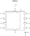
- FIG. 2 is an external rear view of the semiconductor device of the embodiment.
- FIG. 3 is an external perspective view of the semiconductor device of the embodiment.
- a semiconductor device 10 is configured as a power device (power transistor), for example.
- the semiconductor device 10 is not limited to this example, and may be any other device.
- an X-axis, a Y-axis, and a Z-axis are defined in the present specification for convenience.
- the X-axis, Y-axis, and Z-axis are orthogonal one another.
- the X axis is provided along a width of the semiconductor device 10.
- the Y axis is provided along a length (depth) of the semiconductor device 10.
- the Z-axis is provided along a thickness of the semiconductor device 10.
- the X direction is a direction along the X-axis, and includes a +X direction indicated by an arrow of the X-axis and a -X direction being the opposite direction of the arrow of the X-axis.
- the Y direction is a direction along the Y-axis, and includes a +Y direction indicated by an arrow of the Y-axis and a -Y direction being the opposite direction of the arrow of the Y-axis.
- the Z direction is a direction along the Z-axis, and includes a +Z direction indicated by an arrow of the Z-axis and a -Z direction being the opposite direction of the arrow of the Z-axis.
- the semiconductor device 10 includes a resin mold 11, first connectors 12, second connectors 13, third connectors 14, and a fourth connector 15.
- the first connectors 12 and the second connectors 13 constitute part of a first lead frame.
- the third connectors 14 function as a third lead frame, and the fourth connector 15 function as a second lead frame.
- the first connectors 12 (four in an example of FIG. 1 ) are provided to each extend in the -X direction from the resin mold 11.
- the second connectors 13 are provided such that one of them extends in the +Y direction and the other extends in the -Y direction from the resin mold 11.
- the third connectors 14 (three in the example of FIG. 1 ) are provided to each extend in the +X direction from the resin mold 11.
- the fourth connector 15 is provided to extend in the +X direction from the resin mold 11.
- the first connectors 12 and the second connectors 13 function as a lead frame, as described above, and are exposed from the resin mold 11 as illustrated in FIG. 2 for heat dissipation of the semiconductor chips, which will be described later.
- the resin mold 11 seals parts of the first connectors 12 to the fourth connector 15, the semiconductor chip, part of the first lead frame, the second lead frame, and a third lead frame, which will be described below.
- FIG. 4 is a front view of the semiconductor device of the embodiment before molding.
- the semiconductor device 10 includes a first lead frame 22 on which a semiconductor chip 21 is mounted.
- the semiconductor chip 21 is a vertical device such as a vertical metal-oxide-semiconductor field effect transistor (MOSFET).
- MOSFET vertical metal-oxide-semiconductor field effect transistor
- the semiconductor chip 10 is not limited to this example, but may be a vertical insulated gate bipolar transistor (IGBT), a vertical diode, or any other desired semiconductor chip.
- IGBT vertical insulated gate bipolar transistor
- the semiconductor chip 21 contains silicon (Si) as a semiconductor.
- the semiconductor chip 21 is not limited to this example, but may also include a compound semiconductor that is different from silicon, such as SiC or GaN.
- a gate terminal TG and a source terminal TS are provided on the front side (a side located in the +Z direction) of the semiconductor chip 21.
- the gate terminal TG does not carry current, so that the gate terminal TG is provided to have a smaller area than the source terminal TS.
- the gate terminal TG has a rectangular shape in plan view and is disposed along the X-axis.
- a drain terminal which is not illustrated, is provided on the rear side of the semiconductor chip 21 (a face located in the -Z direction).
- the drain terminal of the semiconductor chip 21 is electrically connected to the first lead frame 22 with lead solder serving as a conductive adhesive.
- lead solder serving as a conductive adhesive.
- the semiconductor chip 21 is mechanically fixed to the first lead frame 22 and thereby becomes a predetermined thermal conducting state. This enables the semiconductor chip 21 to dissipate the heat thereof through the first lead frame 22.
- the three ends of the first lead frame 22 (a left end, a top end, and a bottom end in an example of FIG. 4 ) constitute the first and second connectors 12 and 13, which function as drain terminals TD.
- One end of a second lead frame 23A constitutes the fourth connector 15 functioning as the gate terminal TG.
- One end of a third lead frame 23B constitutes the third connectors 14 functioning as the source terminal TS.
- a metal (Cu) connector 24A which functions as a conductive member, is mechanically and electrically connected to between the gate terminal TG of the semiconductor chip 21 and the second lead frame 23A with lead solder serving as a conductive adhesive.
- a metal (Cu) connector 24B which functions as a conductive member, is mechanically and electrically connected to between the source terminal TS of the semiconductor chip 21 and the 32nd lead frame 23 with lead solder serving as a conductive adhesive.
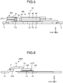
- FIG. 5 is a bottom view of the semiconductor device of the embodiment before molding, that is, a left end view of the semiconductor device 10 based on FIG. 4 .
- the metal connector 24A includes a connection portion 31, an extension portion 32, an arm portion 33, and a connection portion 34, which are disposed in the -X direction toward a position where the gate terminal TG of the semiconductor chip 21 is provided.
- the metal connector 24A has an L-shape.
- connection portion 31 has a rectangular shape, and includes a first connection face 31A provided on the rear side thereof (-Z direction).
- the extension portion 32 extends from the connection portion 31 in the -Y direction, and then extends in the -X direction to connect to the arm portion 33.
- the arm portion 33 connects to the connection portion 34 while extending in the -X direction and the +Y direction to reach the gate terminal TG.
- the connection portion 34 includes a second connection face 36 on the rear side (-Z direction). The second connection face 36 is mechanically and electrically connected to the gate terminal TG.
- connection portion 34 of the metal connector 24A is mechanically and electrically connected to the gate terminal TG with lead solder serving as a conductive adhesive on the second connection face 34A.
- lead solder serving as a conductive adhesive on the second connection face 34A.
- the second lead frame 23A is located, apart from the first lead frame 22, on the rear side (-Z direction) of the connection portion 31.
- a first connection face 31A of the connection portion 31 is mechanically and electrically connected to the second lead frame 23A with lead solder serving as a conductive adhesive.
- the metal connector 24A electrically connects the gate terminal TG of the semiconductor chip 21 to the second lead frame 23A through the lead solder.
- the metal connector 24B as illustrated in FIGS. 4 and 5 , includes a connection portion 41, an extension portion 42, an arm portion 43, and a connection portion 44, which are disposed in the -X direction toward the position where the source terminal TS of the semiconductor chip 21 is provided.
- the metal connector 24B has an L-shape.
- the connection portion 41 includes a first connection face on the rear side (-Z direction).
- the extension portion 42 extends from the connection portion 41 in the +Z direction, and then extends in the -X direction to connect to the arm portion 43.
- the arm portion 43 connects to the connection portion 44 while extending in the -X and +Y directions so as to reach the source terminal TS.
- the connection portion 44 includes a second connection face on the rear side (-Z direction). The second connection face is mechanically and electrically connected to the source terminal TS.
- connection portion 44 of the third lead frame 23B is mechanically and electrically connected to the source terminal TS with lead solder serving as a conductive adhesive.
- the third lead frame 23B is located, apart from the first lead frame 22, on the rear side (-Z direction) of the connection portion 41.
- the first connection face of the connection portion 41 is mechanically and electrically connected to the third lead frame 23B with lead solder serving as a conductive adhesive.
- FIG. 6 is an explanatory view of the problem of a conventional semiconductor device before molding.
- the same signs are used for the same parts as in FIG. 5 .
- connection portion 31 In a conventional metal connector 24AP, a connection portion 31, an extension portion 32, an arm portion 33, and a connection portion 34P are disposed in the -X direction toward the position where a gate terminal TG of a semiconductor chip 21 is provided.
- the connection portion 31 includes the first connection face on the rear side (-Z direction).
- the extension portion 32 extends from the connection portion 31 in the -Y direction, and then extends in the -X direction to connect to the arm portion 33.
- the arm portion 33 connects to the connection portion 34 while extending in the -X direction and the +Y direction so as to reach the gate terminal TG.
- the connection portion 34P extends straight in the -X direction along the X-Z plane.
- a second connection face mechanically and electrically connected to the gate terminal TG is provided on the rear side (-Z direction) of the connection portion 34P.
- connection portion 34P of the metal connector 24AP extends along the gate terminal TG which is disposed along the X-Z plane.
- the connection portion 34P is located at a position where the connection portion 34P is electrically connected to the gate terminal TG with lead solder serving as a conductive adhesive.
- the metal connector 24AP is generally processed by punching and bending in a single process with a press machine.
- the most part of the connection portion 34P, especially the second connection face, is a rolled face, whereas a tip portion 34PT of the connection portion 34P is a cut face.
- the tip portion 34PT of the connection portion 34P has a greater roughness than the rolled face does.
- the wetting of lead solder serving as a conductive adhesive is poor. Therefore, when reflow processing is performed, there is a possibility a defective joint of lead solder occurs in the area of the circle AR in FIG. 6 , resulting in a defective product.
- FIG. 7 is a side view of the semiconductor device of the embodiment before molding.
- FIG. 8 is an external perspective view of the semiconductor device of the embodiment before molding.
- the connection portion 31, the extension portion 32, the arm portion 33, and the connection portion 34 are disposed in the -X direction toward a position where the gate terminal TG of the semiconductor chip 21 is provided.
- connection portion 31 includes the first connection face 31A on the rear side (-Z direction).
- the extension portion 32 extends from the connection portion 31 in the -Y direction, and then extends in the -X direction to connect to the arm portion 33.
- the arm portion 33 connects to the connection portion 34 while extending in the -X direction and the +Y direction so as to reach the gate terminal TG.
- the connection portion 34 includes a second connection face 36 on the rear side (-Z direction). The second connection face 36 is mechanically and electrically connected to the gate terminal TG.
- connection portion 34 of the metal connector 24A is disposed along the gate terminal TG, that is, disposed in a state of extending in the X-axis direction.
- the connection portion 34 is located in a position where it is electrically connected to the gate terminal TG with lead solder serving as a conductive adhesive.
- the metal connector 24A is generally processed by punching and bending in a single process by a press machine, and a tip portion 34T of the connection portion 34 is a cut face.
- the tip portion 34T is gradually bent in a direction separating from the gate terminal TG as an electrode to be bonded, that is, gradually bent in the +Z direction.
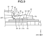
- FIG. 9 is an enlarged view of the joint of the metal connector 24A.
- the connection portion 34 is gradually bent upward (in the +Z direction) in FIG. 9 through a bending portion 35 with respect to the arm portion 33.
- the tip portion 34T of the connection portion 34 is disposed apart from a bonding face 50 of the gate terminal TG, on which the connection portion 34 is connected with the lead solder as a conductive adhesive. More specifically, the connection portion 34 is gradually bent upward (in the +Z direction) such that the tip portion 34T is disposed at a position where surface tension of the lead solder does not affect the tip portion 34T, that is, a positon where the lead solder does not reach the tip portion 34T.
- a lower face 37 of the arm portion 33 is a rolled face resulting from the bending process for forming the arm portion 33 and the bending portion 35.
- the bending portion 35 is provided in a direction opposite to the tip portion 34T with respect to the bonding face 50.
- the bending portion 35 is bent in a vertical direction (+Z direction) of a formation face 21A of the semiconductor chip 21, on which the gate terminal TG is formed, such that the connection portion 34 separates from the formation face 21A.
- connection face 36 of the connection portion 34 which is to be bonded to the bonding face 50, and a lower face 38 of the connection portion 34 are the rolled faces resulting from the bending process for forming the bending portion 35. This allows the second connection face 36 and the lower face 38 of the connection portion 34 to have a much smaller roughness than the tip portion 34T of the connection portion 34 does.
- the second connection face 36 and the lower face 38 of the connection portion 34 have high wettability. Therefore, with the surface tension and capillary action of the lead solder, the second connection face 36 and the lower face 38 of the connection portion 34 are firmly bonded to the bonding face 50 of the gate terminal TG.
- the shapes in front view of the second connection face 36 and the bonding face 50 are each a rectangular shape in which an extending direction of the connection portion 34 is a longitudinal direction. This makes it possible, with the surface tension of lead solder, to suppress the rotation of the connection portion 34 so as to be fixed in a predetermined position even during reflow processing.
- the lower face 38 on a lower end 35T of the bending portion 35 is also a rolled face resulting from the bending process for forming the bending portion 35, and is disposed on a side within a predetermined distance (in the -X direction in FIG. 9 ) from the end of the gate electrode TG, so that the surface tension of the lead solder causes the lead solder to reach the surface of the gate electrode TG on the left side of the metal connector 24A in FIG. 9 , and the metal connector 24A can be more firmly bonded, making it possible to improve crack resistance of the metal connector 24A.
- the present embodiment makes it possible to control the behavior of the metal connector 24A during reflow processing, and to suppress the defective joint of the metal connector and the misalignment of the bonding position of the metal connector without changing a manufacturing process.
- bonding is possible with lead solder serving as a conductive adhesive entirely spreading over the second connection face 36 and the bonding face 50 of the gate terminal TG, making it possible to improve the crack resistance.
- the front view shapes of the second connection face 36 and the bonding face 50 are each a rectangular shape, but this is not limited thereto from the viewpoint of suppressing the defective joint of the metal connectors.
- any desired shape can be applied to the second connection face 36 and the bonding face 50, such as square, circular, oval, diamond, or the like.
- a shape having a large aspect ratio for example, elliptical shape, diamond shape, etc. is desirable.
- the bending portion 35 is provided so as to gradually bend the connection portion 34 in the vertical direction (+Z direction) apart from the formation face 21A of the gate electrode TG, and thereby the cut face (34T) is separated from the bonding face (50).
- the metal connector (24A) may be constructed without the bending portion 35.
- the connection portion 34 is provided to extend in a horizontal direction (-X direction along the X-Y plane in the example of FIG. 7 ), and the thickness of the area near the tip portion 34T is thinned by pressing so as to separate the tip portion 34T from the bonding face 50 in the +Z direction.
- This structure also allows the bonding face 50 to have only the rolled face of the metal connector 24 thereon, improving the wettability of lead solder serving as a conductive adhesive.
Landscapes
- Lead Frames For Integrated Circuits (AREA)
- Noodles (AREA)
- Mechanical Treatment Of Semiconductor (AREA)
- Bipolar Transistors (AREA)
- Die Bonding (AREA)
Abstract
A semiconductor device of an embodiment includes a first lead frame (22), a second lead frame (23A) located apart from the first lead frame, a semiconductor chip (21) mounted on the first lead frame, and a conductive member (24A). The conductive member (24A) electrically connects an electrode (TG) of the semiconductor chip to the second lead frame through a conductive adhesive. The conductive member (24A) includes a cut face (34T) located apart from a bonding face (50) of the electrode, on which the conductive member is bonded.
Description
- Embodiments described herein relate generally to a semiconductor device.
- There is a known semiconductor device in which a lead frame and an electrode of a semiconductor chip are electrically connected by, for example, a plate-shaped connector. Mechanical and electrical connection is made by conductive adhesives, such as solder, between the electrode and the connector, and between the lead frame and the connector.
- A reflow furnace is used in a bonding process for a semiconductor package manufactured by bonding a silicon (Si) chip to a lead frame and a copper (Cu) connector with lead solder and sealing them by molding.
- There is a problem that a copper connector with poor solder wettability during a reflow process causes a defective joint, resulting in a defective product in terms of solder joint reliability.
-
-
FIG. 1 is an external front view of the semiconductor device of an embodiment; -
FIG. 2 is an external rear view of the semiconductor device of the embodiment; -
FIG. 3 is an external perspective view of the semiconductor device of the embodiment; -
FIG. 4 is a front view of the semiconductor device of the embodiment before molding; -
FIG. 5 is a bottom view of the semiconductor device of the embodiment before molding; -
FIG. 6 is an explanatory view of a problem of a conventional semiconductor device before molding; -
FIG. 7 is a side view of the semiconductor device of the embodiment before molding; -
FIG. 8 is an external perspective view of the semiconductor device of the embodiment before molding; and -
FIG. 9 is an enlarged view of a joint of a metal connector. - A semiconductor device of an embodiment includes a first lead frame, a second lead frame located apart from the first lead frame, a semiconductor chip mounted on the first lead frame, and a conductive member. The conductive member electrically connects an electrode of the semiconductor chip to the second lead frame through a conductive adhesive. The conductive member includes a cut face located apart from a bonding face of the electrode, on which the conductive member is bonded.
- The following describes the embodiment with reference to the drawings. In the present specification, components according to the embodiment and descriptions of the components may be described in a plural form. The components and their descriptions are examples and are not limited by the expressions in the present specification. The components may be identified by names different from those in the present specification. The components may also be described by different expressions than those in the present specification.
-
FIG. 1 is an external front view of the semiconductor device of the embodiment.FIG. 2 is an external rear view of the semiconductor device of the embodiment.FIG. 3 is an external perspective view of the semiconductor device of the embodiment. Asemiconductor device 10 is configured as a power device (power transistor), for example. Thesemiconductor device 10 is not limited to this example, and may be any other device. - As illustrated in each of the drawings, an X-axis, a Y-axis, and a Z-axis are defined in the present specification for convenience. The X-axis, Y-axis, and Z-axis are orthogonal one another. The X axis is provided along a width of the
semiconductor device 10. The Y axis is provided along a length (depth) of thesemiconductor device 10. The Z-axis is provided along a thickness of thesemiconductor device 10. - Moreover, an X direction, a Y direction, and a Z direction are defined in the present specification. The X direction is a direction along the X-axis, and includes a +X direction indicated by an arrow of the X-axis and a -X direction being the opposite direction of the arrow of the X-axis. The Y direction is a direction along the Y-axis, and includes a +Y direction indicated by an arrow of the Y-axis and a -Y direction being the opposite direction of the arrow of the Y-axis. The Z direction is a direction along the Z-axis, and includes a +Z direction indicated by an arrow of the Z-axis and a -Z direction being the opposite direction of the arrow of the Z-axis.
- As illustrated in
FIG. 1 , thesemiconductor device 10 includes aresin mold 11,first connectors 12,second connectors 13,third connectors 14, and afourth connector 15. In this configuration, thefirst connectors 12 and thesecond connectors 13 constitute part of a first lead frame. Thethird connectors 14 function as a third lead frame, and thefourth connector 15 function as a second lead frame. The first connectors 12 (four in an example ofFIG. 1 ) are provided to each extend in the -X direction from theresin mold 11. Thesecond connectors 13 are provided such that one of them extends in the +Y direction and the other extends in the -Y direction from theresin mold 11. The third connectors 14 (three in the example ofFIG. 1 ) are provided to each extend in the +X direction from theresin mold 11. Thefourth connector 15 is provided to extend in the +X direction from theresin mold 11. - The
first connectors 12 and thesecond connectors 13 function as a lead frame, as described above, and are exposed from theresin mold 11 as illustrated inFIG. 2 for heat dissipation of the semiconductor chips, which will be described later. - The
resin mold 11 seals parts of thefirst connectors 12 to thefourth connector 15, the semiconductor chip, part of the first lead frame, the second lead frame, and a third lead frame, which will be described below. -
FIG. 4 is a front view of the semiconductor device of the embodiment before molding. Thesemiconductor device 10 includes afirst lead frame 22 on which asemiconductor chip 21 is mounted. - The
semiconductor chip 21 is a vertical device such as a vertical metal-oxide-semiconductor field effect transistor (MOSFET). Thesemiconductor chip 10 is not limited to this example, but may be a vertical insulated gate bipolar transistor (IGBT), a vertical diode, or any other desired semiconductor chip. - The
semiconductor chip 21 contains silicon (Si) as a semiconductor. Thesemiconductor chip 21 is not limited to this example, but may also include a compound semiconductor that is different from silicon, such as SiC or GaN. - In this case, a gate terminal TG and a source terminal TS are provided on the front side (a side located in the +Z direction) of the
semiconductor chip 21. The gate terminal TG does not carry current, so that the gate terminal TG is provided to have a smaller area than the source terminal TS. - In the present embodiment, the gate terminal TG has a rectangular shape in plan view and is disposed along the X-axis.
- A drain terminal, which is not illustrated, is provided on the rear side of the semiconductor chip 21 (a face located in the -Z direction). The drain terminal of the
semiconductor chip 21 is electrically connected to thefirst lead frame 22 with lead solder serving as a conductive adhesive. As a result, thesemiconductor chip 21 is mechanically fixed to thefirst lead frame 22 and thereby becomes a predetermined thermal conducting state. This enables thesemiconductor chip 21 to dissipate the heat thereof through thefirst lead frame 22. - The three ends of the first lead frame 22 (a left end, a top end, and a bottom end in an example of
FIG. 4 ) constitute the first andsecond connectors second lead frame 23A constitutes thefourth connector 15 functioning as the gate terminal TG. One end of athird lead frame 23B constitutes thethird connectors 14 functioning as the source terminal TS. - A metal (Cu)
connector 24A, which functions as a conductive member, is mechanically and electrically connected to between the gate terminal TG of thesemiconductor chip 21 and thesecond lead frame 23A with lead solder serving as a conductive adhesive. - Similarly, a metal (Cu)
connector 24B, which functions as a conductive member, is mechanically and electrically connected to between the source terminal TS of thesemiconductor chip 21 and the 32nd lead frame 23 with lead solder serving as a conductive adhesive. -
FIG. 5 is a bottom view of the semiconductor device of the embodiment before molding, that is, a left end view of thesemiconductor device 10 based onFIG. 4 . As illustrated inFIGS. 4 and5 , themetal connector 24A includes aconnection portion 31, anextension portion 32, anarm portion 33, and aconnection portion 34, which are disposed in the -X direction toward a position where the gate terminal TG of thesemiconductor chip 21 is provided. Themetal connector 24A has an L-shape. - The
connection portion 31 has a rectangular shape, and includes afirst connection face 31A provided on the rear side thereof (-Z direction). Theextension portion 32 extends from theconnection portion 31 in the -Y direction, and then extends in the -X direction to connect to thearm portion 33. - The
arm portion 33 connects to theconnection portion 34 while extending in the -X direction and the +Y direction to reach the gate terminal TG. Theconnection portion 34 includes asecond connection face 36 on the rear side (-Z direction). Thesecond connection face 36 is mechanically and electrically connected to the gate terminal TG. - In the above structure, the
connection portion 34 of themetal connector 24A is mechanically and electrically connected to the gate terminal TG with lead solder serving as a conductive adhesive on the second connection face 34A. The connection state of theconnection portion 34 will be described in detail later. - The
second lead frame 23A is located, apart from thefirst lead frame 22, on the rear side (-Z direction) of theconnection portion 31. Afirst connection face 31A of theconnection portion 31 is mechanically and electrically connected to thesecond lead frame 23A with lead solder serving as a conductive adhesive. As a result, themetal connector 24A electrically connects the gate terminal TG of thesemiconductor chip 21 to thesecond lead frame 23A through the lead solder. - The
metal connector 24B, as illustrated inFIGS. 4 and5 , includes aconnection portion 41, anextension portion 42, anarm portion 43, and aconnection portion 44, which are disposed in the -X direction toward the position where the source terminal TS of thesemiconductor chip 21 is provided. - The
metal connector 24B has an L-shape. Theconnection portion 41 includes a first connection face on the rear side (-Z direction). Theextension portion 42 extends from theconnection portion 41 in the +Z direction, and then extends in the -X direction to connect to thearm portion 43. - The
arm portion 43 connects to theconnection portion 44 while extending in the -X and +Y directions so as to reach the source terminal TS. Theconnection portion 44 includes a second connection face on the rear side (-Z direction). The second connection face is mechanically and electrically connected to the source terminal TS. - In the above structure, the
connection portion 44 of thethird lead frame 23B is mechanically and electrically connected to the source terminal TS with lead solder serving as a conductive adhesive. - The
third lead frame 23B is located, apart from thefirst lead frame 22, on the rear side (-Z direction) of theconnection portion 41. The first connection face of theconnection portion 41 is mechanically and electrically connected to thethird lead frame 23B with lead solder serving as a conductive adhesive. - The following describes advantages of the embodiment. First, a conventional problem will be described.
FIG. 6 is an explanatory view of the problem of a conventional semiconductor device before molding. InFIG. 6 , the same signs are used for the same parts as inFIG. 5 . - In a conventional metal connector 24AP, a
connection portion 31, anextension portion 32, anarm portion 33, and aconnection portion 34P are disposed in the -X direction toward the position where a gate terminal TG of asemiconductor chip 21 is provided. Theconnection portion 31 includes the first connection face on the rear side (-Z direction). Theextension portion 32 extends from theconnection portion 31 in the -Y direction, and then extends in the -X direction to connect to thearm portion 33. - The
arm portion 33 connects to theconnection portion 34 while extending in the -X direction and the +Y direction so as to reach the gate terminal TG. Theconnection portion 34P extends straight in the -X direction along the X-Z plane. In theconnection portion 34P, a second connection face mechanically and electrically connected to the gate terminal TG is provided on the rear side (-Z direction) of theconnection portion 34P. - According to the conventional structure described above, the
connection portion 34P of the metal connector 24AP extends along the gate terminal TG which is disposed along the X-Z plane. Theconnection portion 34P is located at a position where theconnection portion 34P is electrically connected to the gate terminal TG with lead solder serving as a conductive adhesive. Meanwhile, the metal connector 24AP is generally processed by punching and bending in a single process with a press machine. The most part of theconnection portion 34P, especially the second connection face, is a rolled face, whereas a tip portion 34PT of theconnection portion 34P is a cut face. - As a result, the tip portion 34PT of the
connection portion 34P has a greater roughness than the rolled face does. Thus, not only in the tip portion 34PT, but also in the area including the vicinity of the tip portion 34PT illustrated by a circle AR inFIG. 6 , the wetting of lead solder serving as a conductive adhesive is poor. Therefore, when reflow processing is performed, there is a possibility a defective joint of lead solder occurs in the area of the circle AR inFIG. 6 , resulting in a defective product. -
FIG. 7 is a side view of the semiconductor device of the embodiment before molding.FIG. 8 is an external perspective view of the semiconductor device of the embodiment before molding. In themetal connector 24A of the embodiment, as illustrated inFIGS. 7 and 8 , theconnection portion 31, theextension portion 32, thearm portion 33, and theconnection portion 34 are disposed in the -X direction toward a position where the gate terminal TG of thesemiconductor chip 21 is provided. - The
connection portion 31 includes thefirst connection face 31A on the rear side (-Z direction). Theextension portion 32 extends from theconnection portion 31 in the -Y direction, and then extends in the -X direction to connect to thearm portion 33. - The
arm portion 33 connects to theconnection portion 34 while extending in the -X direction and the +Y direction so as to reach the gate terminal TG. Theconnection portion 34 includes asecond connection face 36 on the rear side (-Z direction). Thesecond connection face 36 is mechanically and electrically connected to the gate terminal TG. - In the above structure, the
connection portion 34 of themetal connector 24A is disposed along the gate terminal TG, that is, disposed in a state of extending in the X-axis direction. Theconnection portion 34 is located in a position where it is electrically connected to the gate terminal TG with lead solder serving as a conductive adhesive. - As in the conventional case described above, the
metal connector 24A is generally processed by punching and bending in a single process by a press machine, and atip portion 34T of theconnection portion 34 is a cut face. However, in theconnection portion 34 of the embodiment, thetip portion 34T is gradually bent in a direction separating from the gate terminal TG as an electrode to be bonded, that is, gradually bent in the +Z direction. -
FIG. 9 is an enlarged view of the joint of themetal connector 24A. As illustrated inFIG. 9 , theconnection portion 34 is gradually bent upward (in the +Z direction) inFIG. 9 through a bendingportion 35 with respect to thearm portion 33. In this structure, thetip portion 34T of theconnection portion 34 is disposed apart from abonding face 50 of the gate terminal TG, on which theconnection portion 34 is connected with the lead solder as a conductive adhesive. More specifically, theconnection portion 34 is gradually bent upward (in the +Z direction) such that thetip portion 34T is disposed at a position where surface tension of the lead solder does not affect thetip portion 34T, that is, a positon where the lead solder does not reach thetip portion 34T. - A
lower face 37 of thearm portion 33 is a rolled face resulting from the bending process for forming thearm portion 33 and the bendingportion 35. - The bending
portion 35 is provided in a direction opposite to thetip portion 34T with respect to thebonding face 50. The bendingportion 35 is bent in a vertical direction (+Z direction) of aformation face 21A of thesemiconductor chip 21, on which the gate terminal TG is formed, such that theconnection portion 34 separates from theformation face 21A. - Thus, the
second connection face 36 of theconnection portion 34, which is to be bonded to thebonding face 50, and alower face 38 of theconnection portion 34 are the rolled faces resulting from the bending process for forming the bendingportion 35. This allows thesecond connection face 36 and thelower face 38 of theconnection portion 34 to have a much smaller roughness than thetip portion 34T of theconnection portion 34 does. - As a result, the
second connection face 36 and thelower face 38 of theconnection portion 34 have high wettability. Therefore, with the surface tension and capillary action of the lead solder, thesecond connection face 36 and thelower face 38 of theconnection portion 34 are firmly bonded to thebonding face 50 of the gate terminal TG. The shapes in front view of thesecond connection face 36 and thebonding face 50 are each a rectangular shape in which an extending direction of theconnection portion 34 is a longitudinal direction. This makes it possible, with the surface tension of lead solder, to suppress the rotation of theconnection portion 34 so as to be fixed in a predetermined position even during reflow processing. - Moreover, the
lower face 38 on alower end 35T of the bendingportion 35 is also a rolled face resulting from the bending process for forming the bendingportion 35, and is disposed on a side within a predetermined distance (in the -X direction inFIG. 9 ) from the end of the gate electrode TG, so that the surface tension of the lead solder causes the lead solder to reach the surface of the gate electrode TG on the left side of themetal connector 24A inFIG. 9 , and themetal connector 24A can be more firmly bonded, making it possible to improve crack resistance of themetal connector 24A. - As described above, the present embodiment makes it possible to control the behavior of the
metal connector 24A during reflow processing, and to suppress the defective joint of the metal connector and the misalignment of the bonding position of the metal connector without changing a manufacturing process. - Additionally, bonding is possible with lead solder serving as a conductive adhesive entirely spreading over the
second connection face 36 and thebonding face 50 of the gate terminal TG, making it possible to improve the crack resistance. - In the above description, the front view shapes of the
second connection face 36 and thebonding face 50 are each a rectangular shape, but this is not limited thereto from the viewpoint of suppressing the defective joint of the metal connectors. - For example, any desired shape can be applied to the
second connection face 36 and thebonding face 50, such as square, circular, oval, diamond, or the like. From the viewpoint of preventing rotation during reflow processing of metal connectors, a shape having a large aspect ratio (for example, elliptical shape, diamond shape, etc.) is desirable. - In the
metal connector 24A of the above description, the bendingportion 35 is provided so as to gradually bend theconnection portion 34 in the vertical direction (+Z direction) apart from theformation face 21A of the gate electrode TG, and thereby the cut face (34T) is separated from the bonding face (50). In another embodiment, the metal connector (24A) may be constructed without the bendingportion 35. In such a metal connector, for example, theconnection portion 34 is provided to extend in a horizontal direction (-X direction along the X-Y plane in the example ofFIG. 7 ), and the thickness of the area near thetip portion 34T is thinned by pressing so as to separate thetip portion 34T from thebonding face 50 in the +Z direction. - This structure also allows the
bonding face 50 to have only the rolled face of the metal connector 24 thereon, improving the wettability of lead solder serving as a conductive adhesive. - While certain embodiments have been described, these embodiments have been presented by way of example only, and are not intended to limit the scope of the inventions. Indeed, the novel embodiments described herein may be embodied in a variety of other forms; furthermore, various omissions, substitutions and changes in the form of the embodiments described herein may be made without departing from the spirit of the inventions. The accompanying claims and their equivalents are intended to cover such forms or modifications as would fall within the scope and spirit of the inventions.
Claims (8)
- A semiconductor device (10) comprising:a first lead frame (22);a second lead frame (23A) located apart from the first lead frame;a semiconductor chip (21) mounted on the first lead frame; anda conductive member (24A) electrically connecting an electrode (TG) of the semiconductor chip to the second lead frame through a conductive adhesive,wherein the conductive member (24A) includes a cut face (34T) located apart from a bonding face (50) of the electrode, on which the conductive member is bonded.
- The semiconductor device according to claim 1, whereinthe cut face (34T) is one end of the conductive member (24A), andthe conductive member is bonded to the electrode (TG) at a rolled face of the conductive member.
- The semiconductor device according to claim 1 or claim 2, wherein the conductive member (24A) includes a bending portion (35) for causing the cut face (34T) to be located apart from the bonding face (50), the bending portion being provided in a direction opposite to the cut face with respect to the bonding face.
- The semiconductor device according to claim 3, wherein the bending portion (35) is bent in a direction vertically separating from a formation face (21A) on which the electrode (TG) is provided.
- The semiconductor device according to claim 1, wherein the bonding face (50) has a rectangular shape in a front view, in which an extending direction of the conductive member (24A) is a longitudinal direction.
- The semiconductor device according to claim 2, wherein the bonding face (50) has a rectangular shape in a front view, in which an extending direction of the conductive member (24A) is a longitudinal direction.
- The semiconductor device according to claim 3, wherein the bonding face (50) has a rectangular shape in a front view, in which an extending direction of the conductive member (24A) is a longitudinal direction.
- The semiconductor device according to claim 4, wherein the bonding face (50) has a rectangular shape in a front view, in which an extending direction of the conductive member (24A) is a longitudinal direction.
Applications Claiming Priority (1)
| Application Number | Priority Date | Filing Date | Title |
|---|---|---|---|
| JP2021047248A JP2022146341A (en) | 2021-03-22 | 2021-03-22 | Semiconductor device |
Publications (1)
| Publication Number | Publication Date |
|---|---|
| EP4064338A1 true EP4064338A1 (en) | 2022-09-28 |
Family
ID=79230737
Family Applications (1)
| Application Number | Title | Priority Date | Filing Date |
|---|---|---|---|
| EP21214310.1A Withdrawn EP4064338A1 (en) | 2021-03-22 | 2021-12-14 | Semiconductor device |
Country Status (6)
| Country | Link |
|---|---|
| US (1) | US11929306B2 (en) |
| EP (1) | EP4064338A1 (en) |
| JP (1) | JP2022146341A (en) |
| KR (1) | KR20220131814A (en) |
| CN (1) | CN115117006A (en) |
| TW (1) | TW202238888A (en) |
Families Citing this family (2)
| Publication number | Priority date | Publication date | Assignee | Title |
|---|---|---|---|---|
| JP7720181B2 (en) * | 2021-07-12 | 2025-08-07 | 新電元工業株式会社 | Terminal member and semiconductor device |
| KR102873894B1 (en) * | 2022-12-30 | 2025-10-17 | 하나 마이크로일렉트로닉스 (자싱) 씨오., 엘티디. | Semiconductor device |
Citations (10)
| Publication number | Priority date | Publication date | Assignee | Title |
|---|---|---|---|---|
| JPS63170961U (en) * | 1986-12-04 | 1988-11-07 | Fuji Electric Co Let | Semiconductor element |
| JP2008258649A (en) * | 2008-06-06 | 2008-10-23 | Sanyo Electric Co Ltd | Semiconductor device |
| JP2012104708A (en) * | 2010-11-11 | 2012-05-31 | Shindengen Electric Mfg Co Ltd | Connection plate, joint structure, and semiconductor device |
| JP2015012065A (en) * | 2013-06-27 | 2015-01-19 | 株式会社デンソー | Manufacturing method of semiconductor device |
| US20150221582A1 (en) * | 2014-01-31 | 2015-08-06 | Kabushiki Kaisha Toshiba | Connector frame and semiconductor device |
| US20170207150A1 (en) * | 2016-01-19 | 2017-07-20 | Jmj Korea Co., Ltd. | Clip-bonded semiconductor chip package using metal bumps and method for manufacturing the package |
| EP3483931A1 (en) * | 2017-11-08 | 2019-05-15 | Kabushiki Kaisha Toshiba | Semiconductor device |
| EP3503179A1 (en) * | 2017-12-20 | 2019-06-26 | Nexperia B.V. | Electronic device |
| US20200227279A1 (en) * | 2017-10-26 | 2020-07-16 | Shindengen Electric Manufacturing Co., Ltd. | Method for manufacturing semiconductor device |
| EP3761358A1 (en) * | 2019-07-02 | 2021-01-06 | Nexperia B.V. | A lead frame assembly for a semiconductor device |
Family Cites Families (11)
| Publication number | Priority date | Publication date | Assignee | Title |
|---|---|---|---|---|
| US4673967A (en) * | 1985-01-29 | 1987-06-16 | Texas Instruments Incorporated | Surface mounted system for leaded semiconductor devices |
| JPH01102996A (en) | 1987-10-15 | 1989-04-20 | Mitsubishi Electric Corp | Packaging of electronic parts by reflow soldering |
| JPH03120049U (en) | 1990-03-20 | 1991-12-10 | ||
| JPH0629150U (en) * | 1992-02-10 | 1994-04-15 | 株式会社リコー | IC package lead frame |
| JPH0626280U (en) | 1992-09-04 | 1994-04-08 | 株式会社三協精機製作所 | Lead structure of semiconductor device |
| JPH09232499A (en) * | 1996-02-26 | 1997-09-05 | Canon Inc | Semiconductor device |
| US8669650B2 (en) * | 2011-03-31 | 2014-03-11 | Alpha & Omega Semiconductor, Inc. | Flip chip semiconductor device |
| US8940630B2 (en) * | 2013-02-01 | 2015-01-27 | Invensas Corporation | Method of making wire bond vias and microelectronic package having wire bond vias |
| JP2015138899A (en) * | 2014-01-23 | 2015-07-30 | 株式会社デンソー | Semiconductor device and electronic device |
| JP2015142072A (en) | 2014-01-30 | 2015-08-03 | 株式会社東芝 | semiconductor device |
| KR20160033869A (en) | 2014-09-18 | 2016-03-29 | 제엠제코(주) | Methods of manufacturing clip structure and semiconductor package using the same |
-
2021
- 2021-03-22 JP JP2021047248A patent/JP2022146341A/en active Pending
- 2021-12-14 EP EP21214310.1A patent/EP4064338A1/en not_active Withdrawn
- 2021-12-14 TW TW110146699A patent/TW202238888A/en unknown
- 2021-12-15 US US17/552,148 patent/US11929306B2/en active Active
- 2021-12-21 KR KR1020210183351A patent/KR20220131814A/en not_active Ceased
- 2021-12-27 CN CN202111611775.9A patent/CN115117006A/en active Pending
Patent Citations (10)
| Publication number | Priority date | Publication date | Assignee | Title |
|---|---|---|---|---|
| JPS63170961U (en) * | 1986-12-04 | 1988-11-07 | Fuji Electric Co Let | Semiconductor element |
| JP2008258649A (en) * | 2008-06-06 | 2008-10-23 | Sanyo Electric Co Ltd | Semiconductor device |
| JP2012104708A (en) * | 2010-11-11 | 2012-05-31 | Shindengen Electric Mfg Co Ltd | Connection plate, joint structure, and semiconductor device |
| JP2015012065A (en) * | 2013-06-27 | 2015-01-19 | 株式会社デンソー | Manufacturing method of semiconductor device |
| US20150221582A1 (en) * | 2014-01-31 | 2015-08-06 | Kabushiki Kaisha Toshiba | Connector frame and semiconductor device |
| US20170207150A1 (en) * | 2016-01-19 | 2017-07-20 | Jmj Korea Co., Ltd. | Clip-bonded semiconductor chip package using metal bumps and method for manufacturing the package |
| US20200227279A1 (en) * | 2017-10-26 | 2020-07-16 | Shindengen Electric Manufacturing Co., Ltd. | Method for manufacturing semiconductor device |
| EP3483931A1 (en) * | 2017-11-08 | 2019-05-15 | Kabushiki Kaisha Toshiba | Semiconductor device |
| EP3503179A1 (en) * | 2017-12-20 | 2019-06-26 | Nexperia B.V. | Electronic device |
| EP3761358A1 (en) * | 2019-07-02 | 2021-01-06 | Nexperia B.V. | A lead frame assembly for a semiconductor device |
Also Published As
| Publication number | Publication date |
|---|---|
| JP2022146341A (en) | 2022-10-05 |
| US20220301986A1 (en) | 2022-09-22 |
| CN115117006A (en) | 2022-09-27 |
| KR20220131814A (en) | 2022-09-29 |
| US11929306B2 (en) | 2024-03-12 |
| TW202238888A (en) | 2022-10-01 |
Similar Documents
| Publication | Publication Date | Title |
|---|---|---|
| US11088042B2 (en) | Semiconductor device and production method therefor | |
| US8222718B2 (en) | Semiconductor die package and method for making the same | |
| CN107210279B (en) | Power semiconductor device | |
| US8188587B2 (en) | Semiconductor die package including lead with end portion | |
| JP5497985B2 (en) | Semiconductor package | |
| CN112913009B (en) | Semiconductor device and lead frame material | |
| JP7173487B2 (en) | semiconductor equipment | |
| EP4020547B1 (en) | Packaged electronic device with high thermal dissipation and manufacturing process thereof | |
| KR20120127535A (en) | Press fit terminal and semiconductor device | |
| US11929306B2 (en) | Semiconductor device comprising first and second lead frames | |
| CN112542438A (en) | Semiconductor device with a plurality of semiconductor chips | |
| JP2012043956A (en) | Semiconductor device and power semiconductor device | |
| JP2008294219A (en) | Semiconductor device and manufacturing method thereof | |
| US20230411250A1 (en) | Power converter and power converter manufacturing method | |
| CN113363228A (en) | Semiconductor device with a plurality of semiconductor chips | |
| US20220330429A1 (en) | Semiconductor device and method of manufacturing the same | |
| US9252086B2 (en) | Connector and resin-sealed semiconductor device | |
| US20230092121A1 (en) | Semiconductor device | |
| US20220301987A1 (en) | Semiconductor device | |
| CN114203659A (en) | Multilayer interconnection tape | |
| JP2022143657A (en) | Semiconductor device and manufacturing method thereof | |
| US11682596B2 (en) | Power semiconductor module | |
| JP7537077B2 (en) | Manufacturing method for power semiconductor module | |
| JP2023179843A (en) | Semiconductor device and semiconductor device manufacturing method | |
| WO2025063004A1 (en) | Electronic device and method for manufacturing electronic device |
Legal Events
| Date | Code | Title | Description |
|---|---|---|---|
| PUAI | Public reference made under article 153(3) epc to a published international application that has entered the european phase |
Free format text: ORIGINAL CODE: 0009012 |
|
| STAA | Information on the status of an ep patent application or granted ep patent |
Free format text: STATUS: REQUEST FOR EXAMINATION WAS MADE |
|
| 17P | Request for examination filed |
Effective date: 20211214 |
|
| AK | Designated contracting states |
Kind code of ref document: A1 Designated state(s): AL AT BE BG CH CY CZ DE DK EE ES FI FR GB GR HR HU IE IS IT LI LT LU LV MC MK MT NL NO PL PT RO RS SE SI SK SM TR |
|
| STAA | Information on the status of an ep patent application or granted ep patent |
Free format text: STATUS: THE APPLICATION IS DEEMED TO BE WITHDRAWN |
|
| 18D | Application deemed to be withdrawn |
Effective date: 20230329 |