EP4063541A1 - Gallium arsenide crystal body and gallium arsenide crystal substrate - Google Patents
Gallium arsenide crystal body and gallium arsenide crystal substrate Download PDFInfo
- Publication number
- EP4063541A1 EP4063541A1 EP22169221.3A EP22169221A EP4063541A1 EP 4063541 A1 EP4063541 A1 EP 4063541A1 EP 22169221 A EP22169221 A EP 22169221A EP 4063541 A1 EP4063541 A1 EP 4063541A1
- Authority
- EP
- European Patent Office
- Prior art keywords
- equal
- gallium arsenide
- less
- atoms
- gaas
- Prior art date
- Legal status (The legal status is an assumption and is not a legal conclusion. Google has not performed a legal analysis and makes no representation as to the accuracy of the status listed.)
- Pending
Links
Images



Classifications
-
- C—CHEMISTRY; METALLURGY
- C30—CRYSTAL GROWTH
- C30B—SINGLE-CRYSTAL GROWTH; UNIDIRECTIONAL SOLIDIFICATION OF EUTECTIC MATERIAL OR UNIDIRECTIONAL DEMIXING OF EUTECTOID MATERIAL; REFINING BY ZONE-MELTING OF MATERIAL; PRODUCTION OF A HOMOGENEOUS POLYCRYSTALLINE MATERIAL WITH DEFINED STRUCTURE; SINGLE CRYSTALS OR HOMOGENEOUS POLYCRYSTALLINE MATERIAL WITH DEFINED STRUCTURE; AFTER-TREATMENT OF SINGLE CRYSTALS OR A HOMOGENEOUS POLYCRYSTALLINE MATERIAL WITH DEFINED STRUCTURE; APPARATUS THEREFOR
- C30B11/00—Single-crystal growth by normal freezing or freezing under temperature gradient, e.g. Bridgman-Stockbarger method
-
- C—CHEMISTRY; METALLURGY
- C30—CRYSTAL GROWTH
- C30B—SINGLE-CRYSTAL GROWTH; UNIDIRECTIONAL SOLIDIFICATION OF EUTECTIC MATERIAL OR UNIDIRECTIONAL DEMIXING OF EUTECTOID MATERIAL; REFINING BY ZONE-MELTING OF MATERIAL; PRODUCTION OF A HOMOGENEOUS POLYCRYSTALLINE MATERIAL WITH DEFINED STRUCTURE; SINGLE CRYSTALS OR HOMOGENEOUS POLYCRYSTALLINE MATERIAL WITH DEFINED STRUCTURE; AFTER-TREATMENT OF SINGLE CRYSTALS OR A HOMOGENEOUS POLYCRYSTALLINE MATERIAL WITH DEFINED STRUCTURE; APPARATUS THEREFOR
- C30B11/00—Single-crystal growth by normal freezing or freezing under temperature gradient, e.g. Bridgman-Stockbarger method
- C30B11/003—Heating or cooling of the melt or the crystallised material
-
- C—CHEMISTRY; METALLURGY
- C30—CRYSTAL GROWTH
- C30B—SINGLE-CRYSTAL GROWTH; UNIDIRECTIONAL SOLIDIFICATION OF EUTECTIC MATERIAL OR UNIDIRECTIONAL DEMIXING OF EUTECTOID MATERIAL; REFINING BY ZONE-MELTING OF MATERIAL; PRODUCTION OF A HOMOGENEOUS POLYCRYSTALLINE MATERIAL WITH DEFINED STRUCTURE; SINGLE CRYSTALS OR HOMOGENEOUS POLYCRYSTALLINE MATERIAL WITH DEFINED STRUCTURE; AFTER-TREATMENT OF SINGLE CRYSTALS OR A HOMOGENEOUS POLYCRYSTALLINE MATERIAL WITH DEFINED STRUCTURE; APPARATUS THEREFOR
- C30B11/00—Single-crystal growth by normal freezing or freezing under temperature gradient, e.g. Bridgman-Stockbarger method
- C30B11/007—Mechanisms for moving either the charge or the heater
-
- C—CHEMISTRY; METALLURGY
- C30—CRYSTAL GROWTH
- C30B—SINGLE-CRYSTAL GROWTH; UNIDIRECTIONAL SOLIDIFICATION OF EUTECTIC MATERIAL OR UNIDIRECTIONAL DEMIXING OF EUTECTOID MATERIAL; REFINING BY ZONE-MELTING OF MATERIAL; PRODUCTION OF A HOMOGENEOUS POLYCRYSTALLINE MATERIAL WITH DEFINED STRUCTURE; SINGLE CRYSTALS OR HOMOGENEOUS POLYCRYSTALLINE MATERIAL WITH DEFINED STRUCTURE; AFTER-TREATMENT OF SINGLE CRYSTALS OR A HOMOGENEOUS POLYCRYSTALLINE MATERIAL WITH DEFINED STRUCTURE; APPARATUS THEREFOR
- C30B27/00—Single-crystal growth under a protective fluid
-
- C—CHEMISTRY; METALLURGY
- C30—CRYSTAL GROWTH
- C30B—SINGLE-CRYSTAL GROWTH; UNIDIRECTIONAL SOLIDIFICATION OF EUTECTIC MATERIAL OR UNIDIRECTIONAL DEMIXING OF EUTECTOID MATERIAL; REFINING BY ZONE-MELTING OF MATERIAL; PRODUCTION OF A HOMOGENEOUS POLYCRYSTALLINE MATERIAL WITH DEFINED STRUCTURE; SINGLE CRYSTALS OR HOMOGENEOUS POLYCRYSTALLINE MATERIAL WITH DEFINED STRUCTURE; AFTER-TREATMENT OF SINGLE CRYSTALS OR A HOMOGENEOUS POLYCRYSTALLINE MATERIAL WITH DEFINED STRUCTURE; APPARATUS THEREFOR
- C30B29/00—Single crystals or homogeneous polycrystalline material with defined structure characterised by the material or by their shape
- C30B29/10—Inorganic compounds or compositions
- C30B29/40—AIIIBV compounds wherein A is B, Al, Ga, In or Tl and B is N, P, As, Sb or Bi
-
- C—CHEMISTRY; METALLURGY
- C30—CRYSTAL GROWTH
- C30B—SINGLE-CRYSTAL GROWTH; UNIDIRECTIONAL SOLIDIFICATION OF EUTECTIC MATERIAL OR UNIDIRECTIONAL DEMIXING OF EUTECTOID MATERIAL; REFINING BY ZONE-MELTING OF MATERIAL; PRODUCTION OF A HOMOGENEOUS POLYCRYSTALLINE MATERIAL WITH DEFINED STRUCTURE; SINGLE CRYSTALS OR HOMOGENEOUS POLYCRYSTALLINE MATERIAL WITH DEFINED STRUCTURE; AFTER-TREATMENT OF SINGLE CRYSTALS OR A HOMOGENEOUS POLYCRYSTALLINE MATERIAL WITH DEFINED STRUCTURE; APPARATUS THEREFOR
- C30B29/00—Single crystals or homogeneous polycrystalline material with defined structure characterised by the material or by their shape
- C30B29/10—Inorganic compounds or compositions
- C30B29/40—AIIIBV compounds wherein A is B, Al, Ga, In or Tl and B is N, P, As, Sb or Bi
- C30B29/42—Gallium arsenide
-
- H—ELECTRICITY
- H10—SEMICONDUCTOR DEVICES; ELECTRIC SOLID-STATE DEVICES NOT OTHERWISE PROVIDED FOR
- H10D—INORGANIC ELECTRIC SEMICONDUCTOR DEVICES
- H10D62/00—Semiconductor bodies, or regions thereof, of devices having potential barriers
- H10D62/80—Semiconductor bodies, or regions thereof, of devices having potential barriers characterised by the materials
- H10D62/85—Semiconductor bodies, or regions thereof, of devices having potential barriers characterised by the materials being Group III-V materials, e.g. GaAs
- H10D62/854—Semiconductor bodies, or regions thereof, of devices having potential barriers characterised by the materials being Group III-V materials, e.g. GaAs further characterised by the dopants
Definitions
- the present invention relates to a gallium arsenide crystal body and a gallium arsenide crystal substrate.
- a compound semiconductor substrate such as a gallium arsenide crystal substrate, has been suitably used as a substrate of a semiconductor device. It has been required to develop a compound semiconductor substrate on which a high-quality epitaxial layer can be grown to form a semiconductor device having high characteristics.
- Non-Patent Literature 1 discloses that in order to grow a semi-insulating GaAs (gallium arsenide) crystal, a carbon concentration in the GaAs crystal is adjusted by adjusting an oxygen concentration in a GaAs source material melt.
- NPL 1 T. Bunger et al, "Active Carbon Control During VGF Growth of Semiinsulating GaAs", presented at International Conference on Compound Semiconductor Mfg. (2003) 3.5
- an etching pit density of the gallium arsenide crystal body is more than or equal to 10 cm -2 and less than or equal to 10000 cm -2 , and an oxygen concentration of the gallium arsenide crystal body is less than 7.0 ⁇ 10 15 atoms ⁇ cm -3 .
- an etching pit density of the gallium arsenide crystal substrate is more than or equal to 10 cm -2 and less than or equal to 10000 cm -2 , and an oxygen concentration of the gallium arsenide crystal substrate is less than 7.0 ⁇ 10 15 atoms ⁇ cm -3 .
- Non-Patent Literature 1 In the manufacturing of the GaAs crystal as disclosed in T. Bunger et al, "Active Carbon Control During VGF Growth of Semiinsulating GaAs", presented at International Conference on Compound Semiconductor Mfg. (2003) 3.5 (Non-Patent Literature 1), the oxygen concentration in the GaAs source material melt is high, and oxygen reacts with an added dopant (for example, C (carbon)), with the result that an amount of incorporation of the dopant is decreased. This leads to inefficient adjustment of the insulating property or conductivity of the GaAs crystal, disadvantageously. Moreover, when the oxygen concentration in the GaAs source material melt is high, the grown GaAs crystal is hardened and is likely to be cracked when being processed, thus resulting in a decreased processing yield, disadvantageously.
- an added dopant for example, C (carbon)
- the present disclosure has an object to provide a gallium arsenide crystal body and a gallium arsenide crystal substrate, in each of which an insulating property or conductivity can be efficiently adjusted and each of which is suppressed from being cracked when being processed to result in a high processing yield.
- a gallium arsenide crystal body and a gallium arsenide crystal substrate in each of which an insulating property or conductivity can be efficiently adjusted and each of which is suppressed from being cracked when being processed to result in a high processing yield.
- An EPD (etching pit density) of a GaAs (gallium arsenide) crystal body of the present embodiment is more than or equal to 10 cm -2 and less than or equal to 10000 cm -2 , and an oxygen concentration of the GaAs crystal body is less than 7.0 ⁇ 10 15 atoms ⁇ cm -3 .
- the EPD and oxygen concentration of the GaAs crystal body of the present embodiment are very low. Since the EPD is so low as to be more than or equal to 10 cm -2 and less than or equal to 10000 cm -2 , the GaAs crystal body is less likely to be cracked when being processed, thus resulting in a high processing yield. Moreover, since the oxygen concentration is so low as to be less than 7.0 ⁇ 10 15 atoms ⁇ cm -3 , the insulating property or conductivity of the GaAs crystal can be efficiently adjusted.
- EPD etching pit density
- the EPD of the GaAs crystal body of the present embodiment refers to the number of etch pits, which are generated in the surface when treated with 25 mass % of a KOH (potassium hydroxide) aqueous solution for 30 minutes at 350°C, per unit area.
- the EPD of the GaAs crystal body of the present embodiment is more than or equal to 10 cm -2 and less than or equal to 10000 cm -2 .
- the EPD of the GaAs crystal body is less than or equal to 10000 cm -2 , is preferably less than or equal to 7000 cm -2 , and is more preferably less than or equal to 4000 cm -2 . In view of a current manufacturing technology level for the GaAs crystal body, the EPD of the GaAs crystal body is more than or equal to 10 cm -2 .
- CPAA Charge Particle Activation Analysis
- CPAA is an activation analysis in which a target element is quantified by measuring radiations emitted from radionuclide generated by impacting with high-energy charged particles.
- 3 He or the like is used as the charged particles.
- the oxygen concentration can be also measured by SIMS (Secondary Ion Mass Spectrometry); however, since the detection limit in CPAA is about 2.0 ⁇ 10 14 atoms ⁇ cm -3 while the detection limit in SIMS is about 1 ⁇ 10 16 atoms ⁇ cm -3 , CPAA is suitable for precision measurement of a low oxygen concentration of about more than or equal to 2.0 ⁇ 10 14 atoms ⁇ cm -3 and about less than 7.0 ⁇ 10 15 atoms ⁇ cm -3 .
- SIMS Secondary Ion Mass Spectrometry
- 18 F is used which is generated by a nuclear reaction between 3 He and oxygen, 16 O, in the GaAs crystal body and which undergoes ⁇ + decay with a half-life of 109.73 minutes.
- the GaAs crystal body having been irradiated with 3 He is melted with an acid, and generated 18 F is chemically separated by way of a KBF 4 (potassium tetrafluoroborate) precipitation method.
- Gamma rays of 511 keV which are generated by positron annihilation upon the ⁇ + decay of 18 F, are measured using a Nal detector to determine the number of counts for a specified time after the end of the irradiation by the least squares method.
- the number of counts after the specified time as determined using a standard sample, SiO 2 , in the same manner is used for correction, thereby converting it to the oxygen concentration.
- the oxygen concentration of the GaAs crystal body of the present embodiment is less than 7.0 ⁇ 10 15 atoms ⁇ cm -3 .
- the oxygen concentration is less than 7.0 ⁇ 10 15 atoms ⁇ cm -3 , is preferably less than or equal to 5.0 ⁇ 10 15 atoms ⁇ cm -3 , and is more preferably less than or equal to 3.0 ⁇ 10 15 atoms ⁇ cm -3 .
- the oxygen concentration is more than or equal to 2.0 ⁇ 10 14 atoms ⁇ cm -3 .
- the GaAs crystal body of the present embodiment is often manufactured by, but not particularly limited to, a boat method such as a VB (Vertical Bridgman) method or a VGF (Vertical Gradient Freezing) method as described below, the GaAs crystal body includes a straight body portion having a cylindrical shape, and the diameter of the straight body portion is preferably more than or equal to 100 mm and less than or equal to 305 mm. Even though the diameter of the straight body portion of the GaAs crystal body is so large as to be more than or equal to 100 mm and less than or equal to 305 mm, the etching pit density and the oxygen concentration are very low.
- VB Vertical Bridgman
- VGF Very Gradient Freezing
- the diameter of the straight body portion of the GaAs crystal body is preferably more than or equal to 100 mm, and is more preferably more than or equal to 150 mm.
- the diameter of the straight body portion of the GaAs crystal body is preferably less than or equal to 305 mm, and is more preferably less than or equal to 204 mm.
- an n type conductivity impurity concentration (concentration of an impurity for providing the GaAs crystal body with n type conductivity) of the GaAs crystal body of the present embodiment is preferably more than or equal to 1.0 ⁇ 10 15 atoms ⁇ cm -3 and less than or equal to 1.0 ⁇ 10 20 atoms ⁇ cm -3 .
- the n type conductivity impurity concentration is preferably more than or equal to 1.0 ⁇ 10 15 atoms ⁇ cm -3 , and is more preferably more than or equal to 1.0 ⁇ 10 17 atoms ⁇ cm -3 .
- the n type conductivity impurity concentration is preferably less than or equal to 1.0 ⁇ 10 20 atoms ⁇ cm -3 , and is more preferably less than or equal to 5.0 ⁇ 10 18 atoms ⁇ cm -3 .
- the n type conductivity impurity is not particularly limited, but is preferably silicon in order to effectively provide the GaAs crystal body with n type conductivity. A silicon concentration is measured by GDMS (Glow Discharge Mass Spectrometry).
- the specific resistance of the GaAs crystal body of the present embodiment is preferably more than or equal to 1.2 ⁇ 10 7 ⁇ cm and less than or equal to 5.0 ⁇ 10 8 ⁇ cm, and is more preferably more than or equal to 5.0 ⁇ 10 7 ⁇ cm and less than or equal to 5.0 ⁇ 10 8 ⁇ cm.
- the specific resistance is measured by way of Hall measurement in accordance with the van der Pauw method.
- the semi-insulating impurity for providing the GaAs crystal body of the present embodiment with a semi-insulating property is not particularly limited, but is preferably carbon in order to effectively provide the GaAs crystal body with the semi-insulating property.
- the carbon concentration is preferably more than or equal to 5.0 ⁇ 10 14 atoms ⁇ cm -3 and less than or equal to 1.5 ⁇ 10 16 atoms ⁇ cm -3 , and is more preferably more than or equal to 8.0 ⁇ 10 14 atoms ⁇ cm -3 and less than or equal to 1.3 ⁇ 10 16 atoms ⁇ cm -3 .
- Carbon can be added more effectively as the oxygen concentration of the GaAs crystal body is lower. Hence, a lower oxygen concentration is more preferable in order to increase the carbon concentration.
- the carbon concentration is measured by CPAA (Charged Particle Activ
- the GaAs crystal body of the present embodiment is manufactured by the boat method using a crucible, such as the VB (Vertical Bridgman) method and the VGF (Vertical Gradient Freezing) method, as described below.
- the crucible generally includes boron (PBN (pyrolytic boron nitride) is generally used for crucibles, and a boron oxide film is used as a sealing member on an inner wall surface thereof in contact with a GaAs source material). Accordingly, the GaAs crystal body of the present embodiment includes boron.
- the boron concentration of the GaAs crystal body of the present embodiment is preferably less than or equal to 1.0 ⁇ 10 19 atoms ⁇ cm -3 and is more preferably less than or equal to 8.0 ⁇ 10 18 atoms ⁇ cm -3 .
- the boron concentration of the GaAs crystal body is preferably more than or equal to 5.0 ⁇ 10 16 atoms ⁇ cm -3 .
- the boron concentration is measured by GDMS (Glow Discharge Mass Spectrometry).
- a manufacturing apparatus for the GaAs (gallium arsenide) crystal body in the present embodiment preferably includes a crucible 21, a crucible holder 22, a sealing member 23, heaters 24a, 24b, a closure plate 25, and a chamber 26.
- the Crucible 21 includes a seed crystal holding portion and a crystal growth portion connected onto the seed crystal holding portion.
- the seed crystal holding portion is a hollow cylindrical portion that opens at a side connected to the crystal growth portion and that is provided with a bottom wall at a side opposite thereto. At this portion, a GaAs seed crystal 11 can be held.
- the crystal growth portion includes: a conical portion having a conical shape and connected to the seed crystal holding portion at the small-diameter side in the axial direction; and a hollow cylindrical straight body portion connected to the large-diameter side of the conical portion in the axial direction.
- the crystal growth portion has a function of holding a GaAs source material 13 therein and growing the GaAs crystal body by solidifying heated GaAs source material 13 in a molten state.
- a material of crucible 21 is not particularly limited as long as the material has a high mechanical strength and can withstand a temperature at which the source material is melted.
- PBN pyrolytic boron nitride
- an oxide film 21c is preferably formed on the inner wall surface as a sealing member.
- the boron oxide film include a B 2 O 3 film and the like.
- the B 2 O 3 film can be formed on the inner wall surface of crucible 21 by treating crucible 21, which is composed of PBN, at a high temperature of more than or equal to 1000°C in an atmosphere containing more than or equal to 50 volume % of oxygen.
- a material of sealing member 23 is not particularly limited as long as the material can withstand the temperature at which the source material is melted.
- a boron oxide, such as B 2 O 3 can be employed suitably therefor.
- the plurality of heaters 24a, 24b are normally placed to appropriately control the melting and solidification of GaAs source material 13; however, in order to reduce the EPD and the oxygen concentration in the GaAs crystal body to be grown, a smaller number of inter-heater gaps are preferably provided.
- One inter-heater gap is preferably provided. That is, a smaller number of heaters are preferably provided. Two heaters are preferably provided.
- Closure plate 25 is preferably disposed between GaAs source material 13 and sealing member 23 in order to reduce the oxygen concentration in the GaAs crystal body to be grown.
- a material of closure plate 25 is not particularly limited as long as the material has a high mechanical strength and can withstand a temperature at which the source material is melted.
- PBN pyrolytic boron nitride
- a closure ratio (percentage of the area of the closure plate with respect to the cross sectional area of the straight body portion of crucible 21 perpendicular to the axial direction; the same applies to the description below) of closure plate 25 is preferably more than or equal to 75% and less than or equal to 100% and is more preferably more than or equal to 90% and less than or equal to 98% in order to reduce the EPD and the oxygen concentration in the GaAs crystal body to be grown and prevent breakage of the crucible. It should be noted that with reference to Fig. 2 , closure plate 25 may be provided with an opening 25o for adjusting the closure ratio.
- a method for manufacturing the GaAs crystal body in the present embodiment is preferably based on the boat method, such as the VB (Vertical Bridgman) method or the VGF (Vertical Gradient Freezing) method, using the above-described manufacturing apparatus 20. Further, in order to manufacture a GaAs crystal body having a straight body portion with a large diameter, the VB method is more preferable.
- the method for manufacturing the GaAs crystal body in the present embodiment preferably includes a GaAs seed crystal loading step, a GaAs source material loading step, a closure plate placing step, a sealing member placing step, and a crystal growing step.
- manufacturing apparatus 20 is used to load GaAs seed crystal 11 in the seed crystal holding portion of crucible 21 in the GaAs seed crystal loading step.
- GaAs source material loading step GaAs source material 13 is loaded in the crystal growth portion (the conical portion and the straight body portion) of crucible 21.
- GaAs source material 13 is not particularly limited as long as it is GaAs having high purity (for example, more than or equal to 99.9 mass %).
- a GaAs polycrystal body, a portion of a GaAs single crystal with a poor physical property, or the like is used suitably therefor.
- closure plate placing step closure plate 25 is placed on GaAs source material 13 in crucible 21.
- sealing member placing step sealing member 23 is placed on closure plate 25 in crucible 21.
- crucible 21 in which GaAs seed crystal 11, GaAs source material 13, closure plate 25, and sealing member 23 are disposed in this order from below to above is loaded in crystal apparatus 20.
- Crucible 21 is held by crucible holder 22, and heaters 24a, 24b are disposed to surround crucible 21.
- crucible 21 is heated by supplying electric current to heaters 24a, 24b. Accordingly, GaAs source material 13 is melted into a melt and sealing member 23 is also melted into a liquid sealing member.
- an oxide film is formed in the inner wall of crucible 21 due to oxidation of the material of crucible 21.
- the melt of GaAs source material 13 is stirred by convection currents generated due to local low-temperature portions formed by the presence of inter-heater gap 24abo between heater 24a and heater 24b.
- the stirred GaAs source material 13 is brought into contact with oxide film 21c of the inner wall of crucible 21 and/or sealing member 23, whereby oxygen included in oxide film 21c of the inner wall of crucible 21 and/or sealing member 23 is presumably incorporated into GaAs source material 13.
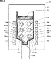
- three or more heaters 34a, 34b, 34c, 34d are disposed. Hence, there are two or more inter-heater gaps 34abo, 34bco, and 34cdo.
- closure plate 25 is disposed between GaAs source material 13 and sealing member 23. Accordingly, contact between GaAs source material 13 and sealing member 23 is suppressed, with the result that oxygen is suppressed from being incorporated into GaAs source material 13.
- a temperature gradient in which a temperature at the GaAs seed crystal 11 side is relatively low and a temperature at the GaAs source material 13 side is relatively high in the axial direction of crucible 21 is formed by moving crucible 21 to the lower side in the axial direction in the case of the VB method or by adjusting the temperature of each of heaters 24a, 24b in the case of the VGF method. Accordingly, molten GaAs source material 13 is sequentially solidified from the GaAs seed crystal 11 side, whereby a GaAs crystal is grown. Molten GaAs source material 13 in the conical portion and straight body portion of the crystal growth portion is entirely solidified in this order, thereby forming the GaAs crystal body.
- a moving speed (pulling-down speed) of crucible 21 is not particularly limited, and can be, for example, more than or equal to 2.0 mm/h and less than or equal to 5.0 mm/h. In this way, the GaAs crystal body having very low EPD and oxygen concentration is obtained.
- the method for manufacturing the GaAs crystal body in the present embodiment As the diameter of the straight body portion of the grown crystal body becomes larger, a temperature difference is more likely to occur in the GaAs melt to more facilitate stirring by convection currents, with the result that the oxygen concentration in the GaAs crystal body is likely to be higher.
- oxygen can be suppressed from being incorporated into the GaAs source material because the contact area between the source material and the sealing member is reduced by placing the closure plate and the convection currents are reduced by an appropriate heater structure and heat environmental design.
- An EPD (etching pit density) of a GaAs (gallium arsenide) crystal substrate of the present embodiment is more than or equal to 10 cm -2 and less than or equal to 10000 cm -2 , and an oxygen concentration of the GaAs crystal substrate is less than 7.0 ⁇ 10 15 atoms ⁇ cm -3 .
- the EPD and oxygen concentration of the GaAs crystal substrate of the present embodiment are very low. Since the EPD is so low as to be more than or equal to 10 cm -2 and less than or equal to 10000 cm -2 , the GaAs crystal substrate is less likely to be cracked when being processed, thus resulting in a high processing yield. Moreover, since the oxygen concentration is so low as to be less than 7.0 ⁇ 10 15 atoms ⁇ cm -3 , the insulating property or conductivity of the GaAs crystal can be efficiently adjusted.
- the oxygen concentration is preferably more than or equal to 2.0 ⁇ 10 14 atoms ⁇ cm -3 and less than or equal to 5.0 ⁇ 10 15 atoms ⁇ cm -3
- the diameter is preferably more than or equal to 100 mm and less than or equal to 305 mm
- the n type conductivity impurity concentration can be more than or equal to 1.0 ⁇ 10 15 atoms ⁇ cm -3 and less than or equal to 1.0 ⁇ 10 20 atoms ⁇ cm -3
- the specific resistance can be more than or equal to 1.2 ⁇ 10 7 ⁇ cm and less than or equal to 5.0 ⁇ 10 8 ⁇ cm
- the boron concentration is preferably less than or equal to 1.0 ⁇ 10 19 atoms ⁇ cm -3 .
- the GaAs crystal substrate of the present embodiment can be obtained by processing and polishing the GaAs crystal body of the first embodiment, and therefore has the same physical properties (EPD, oxygen concentration, diameter, n type conductivity impurity concentration, specific resistance, and boron concentration) as those of the GaAs crystal body of the first embodiment. Hence, these physical properties are not repeatedly described.
- the etching pit density is more than or equal to 10 cm -2 and less than or equal to 10000 cm -2
- the oxygen concentration is more than or equal to 2.0 ⁇ 10 14 atoms ⁇ cm -3 and less than or equal to 5.0 ⁇ 10 15 atoms ⁇ cm -3
- the boron concentration is less than or equal to 1.0 ⁇ 10 19 atoms ⁇ cm -3
- the diameter is more than or equal to 100 mm and less than or equal to 305 mm.
- the GaAs crystal substrate has such a large diameter of more than or equal to 100 mm and less than or equal to 305 mm, the processing yield of the GaAs crystal is high because the etching pit density is low, and the insulating property or conductivity of the GaAs crystal can be efficiently adjusted because the oxygen concentration is very low.
- a method for manufacturing the GaAs crystal substrate in the present embodiment preferably includes a processing step and a polishing step using the GaAs crystal body of the first embodiment in order to efficiently form a GaAs crystal substrate having a low EPD and a low oxygen concentration.
- the processing step the outer circumference of the GaAs crystal body is ground and the GaAs crystal body having been ground is sliced in an appropriately specified direction, thereby obtaining a GaAs crystal substrate having a main surface in the appropriately specified plane orientation.
- the polishing step the main surface of the GaAs crystal substrate is subjected to mechanical polishing and/or chemical mechanical polishing (CMP), thereby obtaining a GaAs crystal substrate having a main surface polished to be a mirror surface.
- CMP chemical mechanical polishing
- a manufacturing apparatus such as one shown in Fig. 1 was used to grow, in accordance with the VB method, four n type conductivity GaAs crystal bodies having different silicon concentrations by adding Si (silicon) as the n type conductivity impurity (Examples 1-1 to 1-5).
- the GaAs source material a GaAs polycrystal having a purity of 99.9 mass % was used.
- a PBN plate was used as the closure plate.
- B 2 O 3 was used as the sealing member.
- the closure ratio of the closure plate and the number of inter-heater gaps were as shown in Table 1.
- Each of the GaAs crystal bodies was grown by adjusting a temperature distribution in the crucible to attain a temperature gradient of less than or equal to 1°C/mm at a crystal growth interface in a crystal growth direction.
- the outer circumference of the obtained GaAs crystal body was ground and the obtained GaAs crystal body was sliced along a plane perpendicular to the crystal growth direction. Then, the main surface thereof was subjected to mechanical polishing and chemical mechanical polishing (CMP), thereby producing GaAs crystal substrates each having a diameter shown in Table 1 and a thickness of more than or equal to 325 ⁇ m and less than or equal to 700 ⁇ m (Examples 1-1 to 1-5).
- CMP chemical mechanical polishing
- the EPD was measured through image analysis by measuring the number of etch pits, which were generated in the surface thereof when the GaAs crystal substrate was soaked in 25 mass % of a KOH aqueous solution at 350°C for 30 minutes, per unit area.
- the oxygen concentration was measured by CPAA (Charged Particle Activation Analysis).
- the silicon concentration and the boron concentration were measured by GDMS (Glow Discharge Mass Spectrometry).
- the specific resistance was measured by way of Hall measurement in accordance with the van der Pauw method. Results thereof are collectively shown in Table 1, Fig. 4 and Fig. 5 .
- Fig. 4 and Fig. 5 include examples other than Examples 1-1 to 1-5.
- a manufacturing apparatus such as one shown in Fig. 1 was used to grow, in accordance with the VB method, five semi-insulating GaAs crystal bodies having different carbon concentrations and specific resistances by adding C (carbon) as the semi-insulating impurity (Examples II-1 to II-5).
- the GaAs source material a GaAs polycrystal having a purity of 99.9 mass % was used.
- a PBN plate was used as the closure plate.
- B 2 O 3 was used as the sealing member.
- the closure ratio of the closure plate and the number of inter-heater gaps were as shown in Table 2.
- Each of the GaAs crystal bodies was grown by adjusting a temperature distribution in the crucible to attain a temperature gradient of less than or equal to 1°C/mm at a crystal growth interface in a crystal growth direction.
- the outer circumference of the obtained GaAs crystal body was ground and the obtained GaAs crystal body was sliced along a plane perpendicular to the crystal growth direction. Then, the main surface thereof was subjected to mechanical polishing and chemical mechanical polishing (CMP), thereby producing GaAs crystal substrates each having a diameter shown in Table 2 and a thickness of more than or equal to 325 ⁇ m and less than or equal to 700 ⁇ m (Examples II-1 to II-5).
- CMP chemical mechanical polishing
- the EPD was measured through image analysis by measuring the number of etch pits, which were generated in the surface thereof when the GaAs crystal substrate was soaked in 25 mass % of a KOH aqueous solution at 350°C for 30 minutes, per unit area.
- the oxygen concentration and the carbon concentration were measured by CPAA (Charged Particle Activation Analysis).
- the boron concentration was measured by GDMS (Glow Discharge Mass Spectrometry).
- the specific resistance was measured by way of Hall measurement in accordance with the van der Pauw method. Results are collectively shown in Table 2, Fig. 4 and Fig. 5 .
- Fig. 4 and Fig. 5 include examples other than Examples II-1 to II-5.
- GaAs crystal bodies and GaAs crystal substrates were produced in the same manner as in Examples I (in the case of n type conductivity) and Examples II (in the case of semi-insulating property) except for manufacturing methods and manufacturing conditions shown in Table 3 (Comparative Examples RI-1 to RI-3 and RII-1 to RII-3).
- each in Comparative Examples RI-1 and RII-1 was manufactured by a LEC (Liquid Encapsulated Czochralski) method, and a GaAs polycrystal having a purity of 99.9 mass % was used as the source material, C (carbon) was used as the semi-insulating impurity, and Si (silicon) was used as the n type conductivity impurity as with Examples I and II described above.
- the EPD, oxygen concentration, silicon concentration or carbon concentration, boron concentration, and specific resistance of each of the obtained GaAs crystal substrates were measured in the same manner as in Examples I or II. Results are collectively shown in Table 3, Fig. 4 and Fig. 5 .
- Example 4 includes comparative examples other than Comparative Examples RI-1 to RI-3 and RII-1 to RII-3.
- Table 1 Examples I Example I-1 Example 1-2 Example 1-3 Example 1-4 Example 1-5 Insulating Property/Conductivity n Type Conductivity n Type Conductivity n Type Conductivity n Type Conductivity Manufacturing Method VB VB VB VB VB VB Closure Ratio of Closure Plate (%) 90 98 98 98 98 Number of Inter-Heater Gaps 4 4 1 4 4 Crystal Substrate Diameter (mm) 101.6 101.6 152.4 152.4 203.2 EPD (cm -2 ) 400 100 1500 10 1800 Oxygen Concentration (atoms ⁇ cm -3 ) 4.30 ⁇ 10 15 3.90 ⁇ 10 14 2.30 ⁇ 10 14 2.20 ⁇ 10 15 8.80 ⁇ 10 14 Silicon Concentration (atoms ⁇ cm 3 ) 5.00 ⁇ 10 18 6.70 ⁇ 10 16 9.20 ⁇ 10 16 6.50 ⁇ 10 17 9.70 ⁇ 10 16 Carbon Concentration (atoms ⁇ cm -3 ) -
- the EPD was so low as to be more than or equal to 10 cm -2 and less than or equal to 10000 cm -2 and the oxygen concentration was so low as to be less than 7.0 ⁇ 10 15 atoms ⁇ cm -3 . Accordingly, a processing yield in processing the GaAs crystal body into the GaAs crystal substrate was so high as to be more than or equal to 90%.
Landscapes
- Chemical & Material Sciences (AREA)
- Engineering & Computer Science (AREA)
- Crystallography & Structural Chemistry (AREA)
- Materials Engineering (AREA)
- Metallurgy (AREA)
- Organic Chemistry (AREA)
- Inorganic Chemistry (AREA)
- Crystals, And After-Treatments Of Crystals (AREA)
Abstract
Description
- The present invention relates to a gallium arsenide crystal body and a gallium arsenide crystal substrate.
- A compound semiconductor substrate, such as a gallium arsenide crystal substrate, has been suitably used as a substrate of a semiconductor device. It has been required to develop a compound semiconductor substrate on which a high-quality epitaxial layer can be grown to form a semiconductor device having high characteristics.
- T. Bunger et al, "Active Carbon Control During VGF Growth of Semiinsulating GaAs", presented at International Conference on Compound Semiconductor Mfg. (2003) 3.5 (Non-Patent Literature 1) discloses that in order to grow a semi-insulating GaAs (gallium arsenide) crystal, a carbon concentration in the GaAs crystal is adjusted by adjusting an oxygen concentration in a GaAs source material melt.
- NPL 1: T. Bunger et al, "Active Carbon Control During VGF Growth of Semiinsulating GaAs", presented at International Conference on Compound Semiconductor Mfg. (2003) 3.5
- In a gallium arsenide crystal body according to the present disclosure, an etching pit density of the gallium arsenide crystal body is more than or equal to 10 cm-2 and less than or equal to 10000 cm-2, and an oxygen concentration of the gallium arsenide crystal body is less than 7.0×10¹⁵ atoms·cm-3.
- In a gallium arsenide crystal substrate according to the present disclosure, an etching pit density of the gallium arsenide crystal substrate is more than or equal to 10 cm-2 and less than or equal to 10000 cm-2, and an oxygen concentration of the gallium arsenide crystal substrate is less than 7.0×10¹⁵ atoms·cm-3.
-
-
Fig. 1 is a schematic cross sectional view showing exemplary manufacturing method and manufacturing apparatus for a gallium arsenide crystal body in the present disclosure. -
Fig. 2 is a schematic plan view showing an exemplary closure plate used in the manufacturing method and manufacturing apparatus for the gallium arsenide crystal body in the present disclosure. -
Fig. 3 is a schematic cross sectional view showing exemplary, typical manufacturing method and manufacturing apparatus for a gallium arsenide crystal body. -
Fig. 4 is a graph showing a relation between an EPD (etching pit density) and an oxygen concentration in a gallium arsenide crystal substrate. -
Fig. 5 is a graph showing a relation between the oxygen concentration and a boron concentration in the gallium arsenide crystal substrate. - In the manufacturing of the GaAs crystal as disclosed in T. Bunger et al, "Active Carbon Control During VGF Growth of Semiinsulating GaAs", presented at International Conference on Compound Semiconductor Mfg. (2003) 3.5 (Non-Patent Literature 1), the oxygen concentration in the GaAs source material melt is high, and oxygen reacts with an added dopant (for example, C (carbon)), with the result that an amount of incorporation of the dopant is decreased. This leads to inefficient adjustment of the insulating property or conductivity of the GaAs crystal, disadvantageously. Moreover, when the oxygen concentration in the GaAs source material melt is high, the grown GaAs crystal is hardened and is likely to be cracked when being processed, thus resulting in a decreased processing yield, disadvantageously.
- In order to solve the above-described problems, the present disclosure has an object to provide a gallium arsenide crystal body and a gallium arsenide crystal substrate, in each of which an insulating property or conductivity can be efficiently adjusted and each of which is suppressed from being cracked when being processed to result in a high processing yield.
- According to the present disclosure, there can be provided a gallium arsenide crystal body and a gallium arsenide crystal substrate, in each of which an insulating property or conductivity can be efficiently adjusted and each of which is suppressed from being cracked when being processed to result in a high processing yield.
- First, embodiments of the present invention are listed and described.
- [1] In a gallium arsenide crystal body according to an embodiment of the present invention, an etching pit density of the gallium arsenide crystal body is more than or equal to 10 cm-2 and less than or equal to 10000 cm-2, and an oxygen concentration of the gallium arsenide crystal body is less than 7.0×10¹⁵ atoms·cm-3. Since the etching pit density and the oxygen concentration are very low in the gallium arsenide crystal body according to the present embodiment, the insulating property or conductivity thereof can be efficiently adjusted and cracking upon processing is suppressed to result in a high processing yield.
- [2] In the gallium arsenide crystal body according to the present embodiment, the oxygen concentration can be more than or equal to 2.0×10¹⁴ atoms·cm-3 and less than or equal to 5.0×10¹⁵ atoms·cm-3. Since the oxygen concentration is much lower in such a gallium arsenide crystal body, the insulating property or conductivity thereof can be efficiently adjusted and cracking upon processing is suppressed to result in a high processing yield.
- [3] The gallium arsenide crystal body according to the present embodiment can include a straight body portion having a cylindrical shape, wherein a diameter of the straight body portion can be more than or equal to 100 mm and less than or equal to 305 mm. Even though the diameter of the straight body portion of such a gallium arsenide crystal body is so large as to be more than or equal to 100 mm and less than or equal to 305 mm, since the etching pit density and the oxygen concentration are very low in the gallium arsenide crystal body, the insulating property or conductivity thereof can be efficiently adjusted and cracking upon processing is suppressed to result in a high processing yield.
- [4] In the gallium arsenide crystal body according to the present embodiment, an n type conductivity impurity concentration of the gallium arsenide crystal body can be more than or equal to 1.0×10¹⁵ atoms·cm-3 and less than or equal to 1.0×10²⁰ atoms·cm-3. Since such a gallium arsenide crystal body has n type conductivity and the etching pit density and the oxygen concentration are very low in the gallium arsenide crystal body, the conductivity thereof can be efficiently adjusted and cracking upon processing is suppressed to result in a high processing yield.
- [5] In the gallium arsenide crystal body according to the present embodiment, a specific resistance of the gallium arsenide crystal body can be more than or equal to 1.2×10⁷ Ω·cm and less than or equal to 5.0×10⁸ Ω·cm. Since such a gallium arsenide crystal body has a semi-insulating property and the etching pit density and oxygen concentration are very low in the gallium arsenide crystal body, the insulating property thereof can be efficiently adjusted and cracking upon processing is suppressed to result in a high processing yield.
- [6] In the gallium arsenide crystal body according to the present embodiment, a boron concentration of the gallium arsenide crystal body can be less than or equal to 1.0×10¹⁹ atoms·cm-3. Since such a gallium arsenide crystal body has excellent quality after the epitaxial growth due to a high dopant activation ratio and the etching pit density and the oxygen concentration are very low in the gallium arsenide crystal body, the conductivity thereof can be efficiently adjusted and cracking upon processing is suppressed to result in a high processing yield.
- [7] In a gallium arsenide crystal substrate according to another embodiment of the present invention, an etching pit density of the gallium arsenide crystal substrate is more than or equal to 10 cm-2 and less than or equal to 10000 cm-2, and an oxygen concentration of the gallium arsenide crystal substrate is less than 7.0×10¹⁵ atoms·cm-3. Since the etching pit density and the oxygen concentration are very low in the gallium arsenide crystal substrate according to the present embodiment, the insulating property or conductivity thereof can be efficiently adjusted and cracking upon processing is suppressed to result in a high processing yield.
- [8] In the gallium arsenide crystal substrate according to the present embodiment, the oxygen concentration can be more than or equal to 2.0×10¹⁴ atoms·cm-3 and less than or equal to 5.0×10¹⁵ atoms·cm-3. Since the oxygen concentration is much lower in such a gallium arsenide crystal substrate, the insulating property or conductivity thereof can be efficiently adjusted and cracking upon processing is suppressed to result in a high processing yield.
- [9] In the gallium arsenide crystal substrate according to the present embodiment, a diameter of the gallium arsenide crystal substrate can be more than or equal to 100 mm and less than or equal to 305 mm. Even though the diameter of such a gallium arsenide crystal substrate is so large as to be more than or equal to 100 mm and less than or equal to 305 mm, since the etching pit density and the oxygen concentration are very low in the gallium arsenide crystal substrate, the insulating property or conductivity thereof can be efficiently adjusted and cracking upon processing is suppressed to result in a high processing yield.
- [10] In the gallium arsenide crystal substrate according to the present embodiment, an n type conductivity impurity concentration of the gallium arsenide crystal substrate can be more than or equal to 1.0×10⁵ atoms·cm-3 and less than or equal to 1.0×10²⁰ atoms·cm-3. Since such a gallium arsenide crystal substrate has n type conductivity and the etching pit density and the oxygen concentration are very low in the gallium arsenide crystal body, the conductivity thereof can be efficiently adjusted and cracking upon processing is suppressed to result in a high processing yield.
- [11] In the gallium arsenide crystal substrate according to the present embodiment, a specific resistance of the gallium arsenide crystal substrate can be more than or equal to 1.2×10⁷ Ω·cm and less than or equal to 5.0×10⁸Ω·cm. Since such a gallium arsenide crystal substrate has a semi-insulating property and the etching pit density and the oxygen concentration are very low in the gallium arsenide crystal substrate, the insulating property thereof can be efficiently adjusted and cracking upon processing is suppressed to result in a high processing yield.
- [12] In the gallium arsenide crystal substrate according to the present embodiment, a boron concentration of the gallium arsenide crystal substrate can be less than or equal to 1.0×10¹⁹ atoms·cm-3. Since such a gallium arsenide crystal substrate has excellent quality after the epitaxial growth due to a high dopant activation ratio and the etching pit density and the oxygen concentration are very low in the gallium arsenide crystal substrate, the conductivity thereof can be efficiently adjusted and cracking upon processing is suppressed to result in a high processing yield.
- [13] In a gallium arsenide crystal substrate according to the present embodiment, an etching pit density of the gallium arsenide crystal substrate can be more than or equal to 10 cm-2 and less than or equal to 10000 cm-2, an oxygen concentration of the gallium arsenide crystal substrate can be more than or equal to 2.0×10¹⁴ atoms·cm-3 and less than or equal to 5.0×10¹⁵ atoms·cm-3, a boron concentration of the gallium arsenide crystal substrate can be less than or equal to 1.0×10¹⁹ atoms·cm-3, and a diameter of the gallium arsenide crystal substrate can be more than or equal to 100 mm and less than or equal to 305 mm. Even though the diameter of such a gallium arsenide crystal substrate is so large as to be more than or equal to 100 mm and less than or equal to 305 mm, since the etching pit density and the oxygen concentration are very low in the gallium arsenide crystal substrate, the insulating property thereof can be efficiently adjusted and cracking upon processing is suppressed to result in a high processing yield.
- An EPD (etching pit density) of a GaAs (gallium arsenide) crystal body of the present embodiment is more than or equal to 10 cm-2 and less than or equal to 10000 cm-2, and an oxygen concentration of the GaAs crystal body is less than 7.0×10¹⁵ atoms·cm-3. The EPD and oxygen concentration of the GaAs crystal body of the present embodiment are very low. Since the EPD is so low as to be more than or equal to 10 cm-2 and less than or equal to 10000 cm-2, the GaAs crystal body is less likely to be cracked when being processed, thus resulting in a high processing yield. Moreover, since the oxygen concentration is so low as to be less than 7.0×10¹⁵ atoms·cm-3, the insulating property or conductivity of the GaAs crystal can be efficiently adjusted.
- The term "EPD (etching pit density)" refers to the number of etch pits (etching pits), which are generated in a crystal surface when the surface is treated with a chemical, per unit area. Specifically, the EPD of the GaAs crystal body of the present embodiment refers to the number of etch pits, which are generated in the surface when treated with 25 mass % of a KOH (potassium hydroxide) aqueous solution for 30 minutes at 350°C, per unit area. The EPD of the GaAs crystal body of the present embodiment is more than or equal to 10 cm-2 and less than or equal to 10000 cm-2. In order to suppress the GaAs crystal body from being cracked when being processed, the EPD of the GaAs crystal body is less than or equal to 10000 cm-2, is preferably less than or equal to 7000 cm-2, and is more preferably less than or equal to 4000 cm-2. In view of a current manufacturing technology level for the GaAs crystal body, the EPD of the GaAs crystal body is more than or equal to 10 cm-2.
- The oxygen concentration is measured by CPAA (Charged Particle Activation Analysis). CPAA is an activation analysis in which a target element is quantified by measuring radiations emitted from radionuclide generated by impacting with high-energy charged particles. In quantifying the oxygen concentration of the GaAs crystal body, 3He or the like is used as the charged particles. The oxygen concentration can be also measured by SIMS (Secondary Ion Mass Spectrometry); however, since the detection limit in CPAA is about 2.0×10¹⁴ atoms·cm-3 while the detection limit in SIMS is about 1×10¹⁶ atoms·cm-3, CPAA is suitable for precision measurement of a low oxygen concentration of about more than or equal to 2.0×10¹⁴ atoms·cm-3 and about less than 7.0×10¹⁵ atoms·cm-3.
- Here, in the CPAA for the oxygen concentration, 18F is used which is generated by a nuclear reaction between 3He and oxygen, 16O, in the GaAs crystal body and which undergoes β+ decay with a half-life of 109.73 minutes. The GaAs crystal body having been irradiated with 3He is melted with an acid, and generated 18F is chemically separated by way of a KBF4 (potassium tetrafluoroborate) precipitation method. Gamma rays of 511 keV, which are generated by positron annihilation upon the β+ decay of 18F, are measured using a Nal detector to determine the number of counts for a specified time after the end of the irradiation by the least squares method. The number of counts after the specified time as determined using a standard sample, SiO2, in the same manner is used for correction, thereby converting it to the oxygen concentration.
- The oxygen concentration of the GaAs crystal body of the present embodiment is less than 7.0×10¹⁵ atoms·cm-3. In order to achieve efficient adjustment of the insulating property or conductivity of the GaAs crystal, the oxygen concentration is less than 7.0×10¹⁵ atoms·cm-3, is preferably less than or equal to 5.0×10¹⁵ atoms·cm-3, and is more preferably less than or equal to 3.0×10¹⁵ atoms·cm-3. In view of the current manufacturing technology level for the GaAs crystal body, the oxygen concentration is more than or equal to 2.0×10¹⁴ atoms·cm-3.
- Since the GaAs crystal body of the present embodiment is often manufactured by, but not particularly limited to, a boat method such as a VB (Vertical Bridgman) method or a VGF (Vertical Gradient Freezing) method as described below, the GaAs crystal body includes a straight body portion having a cylindrical shape, and the diameter of the straight body portion is preferably more than or equal to 100 mm and less than or equal to 305 mm. Even though the diameter of the straight body portion of the GaAs crystal body is so large as to be more than or equal to 100 mm and less than or equal to 305 mm, the etching pit density and the oxygen concentration are very low. In order to achieve low EPD and oxygen concentration in the large-sized GaAs crystal body, the diameter of the straight body portion of the GaAs crystal body is preferably more than or equal to 100 mm, and is more preferably more than or equal to 150 mm. In view of the current manufacturing technology level, the diameter of the straight body portion of the GaAs crystal body is preferably less than or equal to 305 mm, and is more preferably less than or equal to 204 mm.
- In order to provide the GaAs crystal body of the present embodiment with n type conductivity and very low EPD and oxygen concentration, an n type conductivity impurity concentration (concentration of an impurity for providing the GaAs crystal body with n type conductivity) of the GaAs crystal body of the present embodiment is preferably more than or equal to 1.0×10¹⁵ atoms·cm-3 and less than or equal to 1.0×10²⁰ atoms·cm-3. In order to effectively provide the GaAs crystal body with n type conductivity, the n type conductivity impurity concentration is preferably more than or equal to 1.0×10¹⁵ atoms·cm-3, and is more preferably more than or equal to 1.0×10¹⁷ atoms·cm-3. In order to avoid a decreased activation ratio of the dopant, the n type conductivity impurity concentration is preferably less than or equal to 1.0×10²⁰ atoms·cm-3, and is more preferably less than or equal to 5.0×10¹⁸ atoms·cm-3. The n type conductivity impurity is not particularly limited, but is preferably silicon in order to effectively provide the GaAs crystal body with n type conductivity. A silicon concentration is measured by GDMS (Glow Discharge Mass Spectrometry).
- In order to provide the GaAs crystal body of the present embodiment with a semi-insulating property and very low EPD and oxygen concentration, the specific resistance of the GaAs crystal body of the present embodiment is preferably more than or equal to 1.2×10⁷ Ω·cm and less than or equal to 5.0×10⁸ Ω·cm, and is more preferably more than or equal to 5.0×10⁷ Ω·cm and less than or equal to 5.0×10⁸ Ω·cm. The specific resistance is measured by way of Hall measurement in accordance with the van der Pauw method.
- The semi-insulating impurity for providing the GaAs crystal body of the present embodiment with a semi-insulating property is not particularly limited, but is preferably carbon in order to effectively provide the GaAs crystal body with the semi-insulating property. In order to provide the GaAs crystal body with a semi-insulating property with a specific resistance of more than or equal to 1.2×10⁷ Ω·cm and less than or equal to 5.0×10⁸ Ω·cm, the carbon concentration is preferably more than or equal to 5.0×10¹⁴ atoms·cm-3 and less than or equal to 1.5×10¹⁶ atoms·cm-3, and is more preferably more than or equal to 8.0×10¹⁴ atoms·cm-3 and less than or equal to 1.3×10¹⁶ atoms·cm-3. Carbon can be added more effectively as the oxygen concentration of the GaAs crystal body is lower. Hence, a lower oxygen concentration is more preferable in order to increase the carbon concentration. The carbon concentration is measured by CPAA (Charged Particle Activation Analysis).
- The GaAs crystal body of the present embodiment is manufactured by the boat method using a crucible, such as the VB (Vertical Bridgman) method and the VGF (Vertical Gradient Freezing) method, as described below. The crucible generally includes boron (PBN (pyrolytic boron nitride) is generally used for crucibles, and a boron oxide film is used as a sealing member on an inner wall surface thereof in contact with a GaAs source material). Accordingly, the GaAs crystal body of the present embodiment includes boron. In order to prevent a decreased dopant activation ratio in the GaAs crystal body, the boron concentration of the GaAs crystal body of the present embodiment is preferably less than or equal to 1.0×10¹⁹ atoms·cm-3 and is more preferably less than or equal to 8.0×10¹⁸ atoms·cm-3. Moreover, in view of the current manufacturing technology level, the boron concentration of the GaAs crystal body is preferably more than or equal to 5.0×10¹⁶ atoms·cm-3. The boron concentration is measured by GDMS (Glow Discharge Mass Spectrometry).
- With reference to
Fig. 1 , although not particularly limited, in order to efficiently manufacture the GaAs crystal body having an EPD of more than or equal to 10 cm-2 and less than or equal to 10000 cm-2 and an oxygen concentration of less than 7.0×10¹⁵ atoms·cm-3, a manufacturing apparatus for the GaAs (gallium arsenide) crystal body in the present embodiment preferably includes acrucible 21, acrucible holder 22, a sealingmember 23,heaters closure plate 25, and achamber 26. -
Crucible 21 includes a seed crystal holding portion and a crystal growth portion connected onto the seed crystal holding portion. The seed crystal holding portion is a hollow cylindrical portion that opens at a side connected to the crystal growth portion and that is provided with a bottom wall at a side opposite thereto. At this portion, aGaAs seed crystal 11 can be held. The crystal growth portion includes: a conical portion having a conical shape and connected to the seed crystal holding portion at the small-diameter side in the axial direction; and a hollow cylindrical straight body portion connected to the large-diameter side of the conical portion in the axial direction. The crystal growth portion has a function of holding aGaAs source material 13 therein and growing the GaAs crystal body by solidifying heatedGaAs source material 13 in a molten state. - Here, a material of
crucible 21 is not particularly limited as long as the material has a high mechanical strength and can withstand a temperature at which the source material is melted. For example, PBN (pyrolytic boron nitride) can be employed suitably therefor. Moreover, in order to prevent adhesion of GaAs to the inner wall surface ofcrucible 21, anoxide film 21c, such as a boron oxide film, is preferably formed on the inner wall surface as a sealing member. Examples of the boron oxide film include a B2O3 film and the like. For example, the B2O3 film can be formed on the inner wall surface ofcrucible 21 by treatingcrucible 21, which is composed of PBN, at a high temperature of more than or equal to 1000°C in an atmosphere containing more than or equal to 50 volume % of oxygen. - A material of sealing
member 23 is not particularly limited as long as the material can withstand the temperature at which the source material is melted. A boron oxide, such as B2O3, can be employed suitably therefor. - The plurality of
heaters GaAs source material 13; however, in order to reduce the EPD and the oxygen concentration in the GaAs crystal body to be grown, a smaller number of inter-heater gaps are preferably provided. One inter-heater gap is preferably provided. That is, a smaller number of heaters are preferably provided. Two heaters are preferably provided. -
Closure plate 25 is preferably disposed betweenGaAs source material 13 and sealingmember 23 in order to reduce the oxygen concentration in the GaAs crystal body to be grown. A material ofclosure plate 25 is not particularly limited as long as the material has a high mechanical strength and can withstand a temperature at which the source material is melted. For example, PBN (pyrolytic boron nitride) can be employed suitably therefor. A closure ratio (percentage of the area of the closure plate with respect to the cross sectional area of the straight body portion ofcrucible 21 perpendicular to the axial direction; the same applies to the description below) ofclosure plate 25 is preferably more than or equal to 75% and less than or equal to 100% and is more preferably more than or equal to 90% and less than or equal to 98% in order to reduce the EPD and the oxygen concentration in the GaAs crystal body to be grown and prevent breakage of the crucible. It should be noted that with reference toFig. 2 ,closure plate 25 may be provided with an opening 25o for adjusting the closure ratio. - With reference to
Fig. 1 , although not particularly limited, in order to efficiently grow a GaAs (gallium arsenide) crystal body having low EPD and oxygen concentration, a method for manufacturing the GaAs crystal body in the present embodiment is preferably based on the boat method, such as the VB (Vertical Bridgman) method or the VGF (Vertical Gradient Freezing) method, using the above-describedmanufacturing apparatus 20. Further, in order to manufacture a GaAs crystal body having a straight body portion with a large diameter, the VB method is more preferable. Specifically, the method for manufacturing the GaAs crystal body in the present embodiment preferably includes a GaAs seed crystal loading step, a GaAs source material loading step, a closure plate placing step, a sealing member placing step, and a crystal growing step. - First,
manufacturing apparatus 20 is used to loadGaAs seed crystal 11 in the seed crystal holding portion ofcrucible 21 in the GaAs seed crystal loading step. Next, in the GaAs source material loading step,GaAs source material 13 is loaded in the crystal growth portion (the conical portion and the straight body portion) ofcrucible 21. Here,GaAs source material 13 is not particularly limited as long as it is GaAs having high purity (for example, more than or equal to 99.9 mass %). A GaAs polycrystal body, a portion of a GaAs single crystal with a poor physical property, or the like is used suitably therefor. Next, in the closure plate placing step,closure plate 25 is placed onGaAs source material 13 incrucible 21. Next, in the sealing member placing step, sealingmember 23 is placed onclosure plate 25 incrucible 21. - Next, in the crystal growing step,
crucible 21 in whichGaAs seed crystal 11,GaAs source material 13,closure plate 25, and sealingmember 23 are disposed in this order from below to above is loaded incrystal apparatus 20.Crucible 21 is held bycrucible holder 22, andheaters crucible 21. Next,crucible 21 is heated by supplying electric current toheaters GaAs source material 13 is melted into a melt and sealingmember 23 is also melted into a liquid sealing member. Moreover, an oxide film is formed in the inner wall ofcrucible 21 due to oxidation of the material ofcrucible 21. - On this occasion, the melt of
GaAs source material 13 is stirred by convection currents generated due to local low-temperature portions formed by the presence of inter-heater gap 24abo betweenheater 24a andheater 24b. The stirredGaAs source material 13 is brought into contact withoxide film 21c of the inner wall ofcrucible 21 and/or sealingmember 23, whereby oxygen included inoxide film 21c of the inner wall ofcrucible 21 and/or sealingmember 23 is presumably incorporated intoGaAs source material 13. Here, with reference toFig. 3 , in atypical manufacturing apparatus 30, three ormore heaters oxide film 31c of the inner wall ofcrucible 31 and/or sealingmember 33 is incorporated intoGaAs source material 13. On the other hand, with reference toFig. 1 , only twoheaters manufacturing apparatus 20 of the present embodiment. Hence, there is only one inter-heater gap 24abo. Accordingly, fewer convention currents are generated by resultant local low-temperature portions, with the result that oxygen is suppressed from being incorporated intoGaAs source material 13. - Further, in
manufacturing apparatus 20 of the present embodiment,closure plate 25 is disposed betweenGaAs source material 13 and sealingmember 23. Accordingly, contact betweenGaAs source material 13 and sealingmember 23 is suppressed, with the result that oxygen is suppressed from being incorporated intoGaAs source material 13. - Next, a temperature gradient in which a temperature at the
GaAs seed crystal 11 side is relatively low and a temperature at theGaAs source material 13 side is relatively high in the axial direction ofcrucible 21 is formed by movingcrucible 21 to the lower side in the axial direction in the case of the VB method or by adjusting the temperature of each ofheaters GaAs source material 13 is sequentially solidified from theGaAs seed crystal 11 side, whereby a GaAs crystal is grown. MoltenGaAs source material 13 in the conical portion and straight body portion of the crystal growth portion is entirely solidified in this order, thereby forming the GaAs crystal body. In the VB method, a moving speed (pulling-down speed) ofcrucible 21 is not particularly limited, and can be, for example, more than or equal to 2.0 mm/h and less than or equal to 5.0 mm/h. In this way, the GaAs crystal body having very low EPD and oxygen concentration is obtained. - It should be noted that in the method for manufacturing the GaAs crystal body in the present embodiment, as the diameter of the straight body portion of the grown crystal body becomes larger, a temperature difference is more likely to occur in the GaAs melt to more facilitate stirring by convection currents, with the result that the oxygen concentration in the GaAs crystal body is likely to be higher. According to the method for manufacturing the GaAs crystal body in the present embodiment, oxygen can be suppressed from being incorporated into the GaAs source material because the contact area between the source material and the sealing member is reduced by placing the closure plate and the convection currents are reduced by an appropriate heater structure and heat environmental design.
- An EPD (etching pit density) of a GaAs (gallium arsenide) crystal substrate of the present embodiment is more than or equal to 10 cm-2 and less than or equal to 10000 cm-2, and an oxygen concentration of the GaAs crystal substrate is less than 7.0×10¹⁵ atoms·cm-3. The EPD and oxygen concentration of the GaAs crystal substrate of the present embodiment are very low. Since the EPD is so low as to be more than or equal to 10 cm-2 and less than or equal to 10000 cm-2, the GaAs crystal substrate is less likely to be cracked when being processed, thus resulting in a high processing yield. Moreover, since the oxygen concentration is so low as to be less than 7.0×10¹⁵ atoms·cm-3, the insulating property or conductivity of the GaAs crystal can be efficiently adjusted.
- As with the GaAs crystal body of the first embodiment, in the GaAs crystal substrate of the present embodiment, the oxygen concentration is preferably more than or equal to 2.0×10¹⁴ atoms·cm-3 and less than or equal to 5.0×10¹⁵ atoms·cm-3, the diameter is preferably more than or equal to 100 mm and less than or equal to 305 mm, the n type conductivity impurity concentration can be more than or equal to 1.0×10¹⁵ atoms·cm-3 and less than or equal to 1.0×10²⁰ atoms·cm-3, the specific resistance can be more than or equal to 1.2×10⁷ Ω·cm and less than or equal to 5.0×10⁸ Ω·cm, and the boron concentration is preferably less than or equal to 1.0×10¹⁹ atoms·cm-3. As described below, the GaAs crystal substrate of the present embodiment can be obtained by processing and polishing the GaAs crystal body of the first embodiment, and therefore has the same physical properties (EPD, oxygen concentration, diameter, n type conductivity impurity concentration, specific resistance, and boron concentration) as those of the GaAs crystal body of the first embodiment. Hence, these physical properties are not repeatedly described.
- Preferably, in the GaAs crystal substrate of the present embodiment, the etching pit density is more than or equal to 10 cm-2 and less than or equal to 10000 cm-2, the oxygen concentration is more than or equal to 2.0×10¹⁴ atoms·cm-3 and less than or equal to 5.0×10¹⁵ atoms·cm-3, the boron concentration is less than or equal to 1.0×10¹⁹ atoms·cm-3, and the diameter is more than or equal to 100 mm and less than or equal to 305 mm. Even though the GaAs crystal substrate has such a large diameter of more than or equal to 100 mm and less than or equal to 305 mm, the processing yield of the GaAs crystal is high because the etching pit density is low, and the insulating property or conductivity of the GaAs crystal can be efficiently adjusted because the oxygen concentration is very low.
- Although not particularly limited, a method for manufacturing the GaAs crystal substrate in the present embodiment preferably includes a processing step and a polishing step using the GaAs crystal body of the first embodiment in order to efficiently form a GaAs crystal substrate having a low EPD and a low oxygen concentration. In the processing step, the outer circumference of the GaAs crystal body is ground and the GaAs crystal body having been ground is sliced in an appropriately specified direction, thereby obtaining a GaAs crystal substrate having a main surface in the appropriately specified plane orientation. Next, in the polishing step, the main surface of the GaAs crystal substrate is subjected to mechanical polishing and/or chemical mechanical polishing (CMP), thereby obtaining a GaAs crystal substrate having a main surface polished to be a mirror surface.
- A manufacturing apparatus such as one shown in
Fig. 1 was used to grow, in accordance with the VB method, four n type conductivity GaAs crystal bodies having different silicon concentrations by adding Si (silicon) as the n type conductivity impurity (Examples 1-1 to 1-5). As the GaAs source material, a GaAs polycrystal having a purity of 99.9 mass % was used. A PBN plate was used as the closure plate. B2O3 was used as the sealing member. The closure ratio of the closure plate and the number of inter-heater gaps were as shown in Table 1. Each of the GaAs crystal bodies was grown by adjusting a temperature distribution in the crucible to attain a temperature gradient of less than or equal to 1°C/mm at a crystal growth interface in a crystal growth direction. - The outer circumference of the obtained GaAs crystal body was ground and the obtained GaAs crystal body was sliced along a plane perpendicular to the crystal growth direction. Then, the main surface thereof was subjected to mechanical polishing and chemical mechanical polishing (CMP), thereby producing GaAs crystal substrates each having a diameter shown in Table 1 and a thickness of more than or equal to 325 µm and less than or equal to 700 µm (Examples 1-1 to 1-5). The EPD, oxygen concentration, silicon concentration, boron concentration, and specific resistance of each of the obtained GaAs crystal substrates were measured. The EPD was measured through image analysis by measuring the number of etch pits, which were generated in the surface thereof when the GaAs crystal substrate was soaked in 25 mass % of a KOH aqueous solution at 350°C for 30 minutes, per unit area. The oxygen concentration was measured by CPAA (Charged Particle Activation Analysis). The silicon concentration and the boron concentration were measured by GDMS (Glow Discharge Mass Spectrometry). The specific resistance was measured by way of Hall measurement in accordance with the van der Pauw method. Results thereof are collectively shown in Table 1,
Fig. 4 andFig. 5 . Here,Fig. 4 andFig. 5 include examples other than Examples 1-1 to 1-5. - A manufacturing apparatus such as one shown in
Fig. 1 was used to grow, in accordance with the VB method, five semi-insulating GaAs crystal bodies having different carbon concentrations and specific resistances by adding C (carbon) as the semi-insulating impurity (Examples II-1 to II-5). As the GaAs source material, a GaAs polycrystal having a purity of 99.9 mass % was used. A PBN plate was used as the closure plate. B2O3 was used as the sealing member. The closure ratio of the closure plate and the number of inter-heater gaps were as shown in Table 2. Each of the GaAs crystal bodies was grown by adjusting a temperature distribution in the crucible to attain a temperature gradient of less than or equal to 1°C/mm at a crystal growth interface in a crystal growth direction. - The outer circumference of the obtained GaAs crystal body was ground and the obtained GaAs crystal body was sliced along a plane perpendicular to the crystal growth direction. Then, the main surface thereof was subjected to mechanical polishing and chemical mechanical polishing (CMP), thereby producing GaAs crystal substrates each having a diameter shown in Table 2 and a thickness of more than or equal to 325 µm and less than or equal to 700 µm (Examples II-1 to II-5). The EPD, oxygen concentration, carbon concentration, boron concentration, and specific resistance of each of the obtained GaAs crystal substrates were measured. The EPD was measured through image analysis by measuring the number of etch pits, which were generated in the surface thereof when the GaAs crystal substrate was soaked in 25 mass % of a KOH aqueous solution at 350°C for 30 minutes, per unit area. The oxygen concentration and the carbon concentration were measured by CPAA (Charged Particle Activation Analysis). The boron concentration was measured by GDMS (Glow Discharge Mass Spectrometry). The specific resistance was measured by way of Hall measurement in accordance with the van der Pauw method. Results are collectively shown in Table 2,
Fig. 4 andFig. 5 . Here,Fig. 4 andFig. 5 include examples other than Examples II-1 to II-5. - For comparison with Examples I and II, GaAs crystal bodies and GaAs crystal substrates were produced in the same manner as in Examples I (in the case of n type conductivity) and Examples II (in the case of semi-insulating property) except for manufacturing methods and manufacturing conditions shown in Table 3 (Comparative Examples RI-1 to RI-3 and RII-1 to RII-3). It should be noted that each in Comparative Examples RI-1 and RII-1 was manufactured by a LEC (Liquid Encapsulated Czochralski) method, and a GaAs polycrystal having a purity of 99.9 mass % was used as the source material, C (carbon) was used as the semi-insulating impurity, and Si (silicon) was used as the n type conductivity impurity as with Examples I and II described above. The EPD, oxygen concentration, silicon concentration or carbon concentration, boron concentration, and specific resistance of each of the obtained GaAs crystal substrates were measured in the same manner as in Examples I or II. Results are collectively shown in Table 3,
Fig. 4 andFig. 5 . Here,Fig. 4 includes comparative examples other than Comparative Examples RI-1 to RI-3 and RII-1 to RII-3.[Table 1] Examples I Example I-1 Example 1-2 Example 1-3 Example 1-4 Example 1-5 Insulating Property/Conductivity n Type Conductivity n Type Conductivity n Type Conductivity n Type Conductivity n Type Conductivity Manufacturing Method VB VB VB VB VB Closure Ratio of Closure Plate (%) 90 98 98 98 98 Number of Inter-Heater Gaps 4 4 1 4 4 Crystal Substrate Diameter (mm) 101.6 101.6 152.4 152.4 203.2 EPD (cm-2) 400 100 1500 10 1800 Oxygen Concentration (atoms·cm-3) 4.30×10¹⁵ 3.90×10¹⁴ 2.30×10¹⁴ 2.20×10¹⁵ 8.80×10¹⁴ Silicon Concentration (atoms·cm3) 5.00×10¹⁸ 6.70×10¹⁶ 9.20×10¹⁶ 6.50×10¹⁷ 9.70×10¹⁶ Carbon Concentration (atoms·cm-3) - - - - - Boron Concentration (atoms·cm-3) 5.20×10¹⁸ 3.30×10¹⁷ 3.60×10¹⁷ 1.70×10¹⁸ 4.10×10¹⁷ Specific Resistance (Ω·cm) 1.20×10⁻³ 2.80×10⁻² 4.20×10⁻³ 4.60×10⁻³ 3.90×10⁻³ Processing Yield in Processing Crystal Body into Crystal Substrate (%) 92.5 91.2 90.1 91.2 90.2 [Table 2] Examples II Example II-1 Example II-2 Example II-3 Example II-4 Example II-5 Insulating Property/Conductivity Semi-Insulating Property Semi-Insulating Property Semi-Insulating Property Semi-Insulating Property Semi-Insulating Property Manufacturing Method VB VB VB VB VB Closure Ratio of Closure Plate (%) 90 98 98 98 100 Number of Inter-Heater Gaps 4 4 1 4 1 Crystal Substrate Diameter (mm) 101.6 101.6 152.4 152.4 152.4 EPD (cm-2) 5900 3800 4700 6000 9800 Oxygen Concentration (atoms·cm-3) 6.10×10¹⁵ 3.50×10¹⁴ 2.50×10¹⁴ 1.10×10¹⁵ 2.65×10¹⁴ Silicon Concentration (atoms·cm-3) - - - - - Carbon Concentration (atoms·cm-3) 7.10×10¹⁴ 7.00×10¹⁵ 8.30×10¹⁵ 1.20×10¹⁵ 1.40×10¹⁶ Boron Concentration (atoms·cm-3) 2.80×10¹⁷ 8.10×10¹⁶ 7.70×10¹⁶ 1.00×10¹⁷ 6.20×10¹⁶ Specific Resistance (Ω·cm) 1.20×10⁷ 3.20×10⁸ 4.80×10⁸ 2.30×10⁷ 9.00×10⁸ Processing Yield in Processing Crystal Body into Crystal Substrate (%) 92.2 92.7 91.4 92.1 90.3 [Table 3] Comparative Examples Comparative Example RI-1 Comparative Example RI-2 Comparative Example RI-3 Comparative Example RII-1 Comparative Example RII-2 Comparative Example RII-3 Insulating Property/Conductivity n Type Conductivity n Type Conductivity n Type Conductivity Semi-Insulating Property Semi-Insulating Property Semi-Insulating Property Manufacturing Method LEC VB VB LEC VB VB Closure Ratio of Closure Plate (%) 0 0 0 0 0 0 Number of Inter-Heater Gaps 4 4 4 4 4 4 Crystal Substrate Diameter (mm) 101.6 101.6 152.4 101.6 101.6 152.4 EPD (cm-2) 23000 5900 800 99000 9200 4200 Oxygen Concentration (atoms·cm-3) 6.10×10¹⁴ 1.10×10¹⁶ 7.90×10¹⁵ 2.60×10¹⁴ 8.00×10¹⁵ 9.20×10¹⁵ Silicon Concentration (atoms·cm-3) 1.00×10¹⁷ 4.10×10¹⁸ 1.30×10¹⁹ - - - Carbon Concentration (atoms·cm-3) - - - 1.30×10¹⁴ 2.10×10¹⁴ 1.80×10¹⁴ Boron Concentration (atoms·cm-3) 5.30×10¹⁷ 1.20×10¹⁹ 9.10×10¹⁸ 7.70×10¹⁶ 3.70×10¹⁷ 4.40×10¹⁷ Specific Resistance (Ω·cm) 1.10×10⁻² 1.10×10⁻³ 1.30×10⁻³ 9.30×10⁵ 1.30×10⁶ 1.40×10⁶ Processing Yield in Processing Crystal Body into Crystal Substrate (%) 86.1 89.4 89.7 84.8 89.6 88.7 Fig. 4 , in both the cases of the n type conductivity and the semi-insulating property in Examples 1-1 to 1-5 and Examples II-1 to II-5, the EPD was so low as to be more than or equal to 10 cm-2 and less than or equal to 10000 cm-2 and the oxygen concentration was so low as to be less than 7.0×10¹⁵ atoms·cm-3. Accordingly, a processing yield in processing the GaAs crystal body into the GaAs crystal substrate was so high as to be more than or equal to 90%. On the other hand, as shown in Comparative Examples RI-1 and RII-1, in the GaAs crystal bodies and GaAs crystal substrates manufactured by the LEC method in both the cases of the n type conductivity and the semi-insulating property, the EPD was more than 10000 cm-2, with the result that the processing yield in processing the GaAs crystal body into the GaAs crystal substrate was so low as to be less than 90%. Moreover, as shown in Comparative Examples RI-2 to RI-3 and RII-2 to RII-3, in the GaAs crystal bodies and GaAs crystal substrates manufactured by the conventional VB method in both the cases of the n type conductivity and the semi-insulating property, the oxygen concentration was so high as to be more than or equal to 7.0×10¹⁵ atoms·cm-3, with the result that the processing yield in processing the GaAs crystal body into the GaAs crystal substrate was so low as to be less than 90%. - Moreover, with reference to Tables 1 to 3 and
Fig. 5 , in Examples 1-1 to 1-5 and Examples II-1 to II-5, in the both cases of the n type conductivity and the semi-insulating property, there were obtained GaAs crystal substrates in each of which the oxygen concentration was so low as to be less than 7.0×10¹⁵ atoms·cm-3 and the boron concentration was so low as to be less than or equal to 1.0×10¹⁹ atoms·cm-3. - The embodiments and examples disclosed herein are illustrative and non-restrictive in any respect. The scope of the present invention is defined by the terms of the claims, rather than the embodiments and examples described above, and is intended to include any modifications within the scope and meaning equivalent to the terms of the claims.
- 11: GaAs seed crystal; 13: GaAs source material; 21, 31: crucible; 21c, 31c: oxide film; 22, 32: crucible holder; 23, 33: sealing member; 24a, 24b, 34a, 34b, 34c, 34d: heater; 24abo, 34abo, 34bco, 34cdo: inter-heater gap; 25: closure plate; 25o: opening; 26: chamber.
- Further embodiments of this present invention are as follows:
- 1. A gallium arsenide crystal body, wherein
- an etching pit density of the gallium arsenide crystal body is more than or equal to 10 cm-2 and less than or equal to 10000 cm-2,
- an oxygen concentration of the gallium arsenide crystal body is less than 7.0×10¹⁵ atoms·cm-3, and
- a specific resistance of the gallium arsenide crystal body is more than or equal to 1.2×10⁷ Ω·cm and less than or equal to 5.0×10⁸ Ω·cm,
- the gallium arsenide crystal body comprising a straight body portion having a cylindrical shape, wherein a diameter of the straight body portion is more than or equal to 100 mm and less than or equal to 305 mm.
- 2. The gallium arsenide crystal body according to
embodiment 1, wherein the oxygen concentration is more than or equal to 2.0×10¹⁴ atoms·cm-3 and less than or equal to 5.0×10¹⁵ atoms·cm-3. - 3. The gallium arsenide crystal body according to
embodiment 1 orembodiment 2, wherein a boron concentration of the gallium arsenide crystal body is less than or equal to 1.0×10¹⁹ atoms·cm-3. - 4. A gallium arsenide crystal substrate, wherein
- an etching pit density of the gallium arsenide crystal substrate is more than or equal to 10 cm-2 and less than or equal to 10000 cm-2, and
- an oxygen concentration of the gallium arsenide crystal substrate is less than 7.0×10¹⁵ atoms·cm-3,
- a specific resistance of the gallium arsenide crystal substrate is more than or equal to 1.2×10⁷ Ω·cm and less than or equal to 5.0×10⁸ Ω·cm, and
- a diameter of the gallium arsenide crystal substrate is more than or equal to 100 mm and less than or equal to 305 mm.
- 5. The gallium arsenide crystal substrate according to
embodiment 4, wherein the oxygen concentration is more than or equal to 2.0×10¹⁴ atoms·cm-3 and less than or equal to 5.0×10¹⁵ atoms·cm-3. - 6. The gallium arsenide crystal substrate according to
embodiment 4 orembodiment 5, wherein a boron concentration of the gallium arsenide crystal substrate is less than or equal to 1.0×10¹⁹ atoms·cm-3. - 7. The gallium arsenide crystal substrate according to
embodiment 4, wherein- the oxygen concentration is more than or equal to 2.0×10¹⁴ atoms·cm-3 and less than or equal to 5.0×10¹⁵ atoms·cm-3, and
- a boron concentration of the gallium arsenide crystal substrate is less than or equal to 1.0×10¹⁹ atoms·cm-3.
Claims (18)
- A gallium arsenide crystal body, whereinan etching pit density of the gallium arsenide crystal body is more than or equal to 10 cm-2 and less than or equal to 10000 cm-2,an oxygen concentration of the gallium arsenide crystal body is less than 7.0×10¹⁵ atoms·cm-3, andan n type conductivity impurity concentration of the gallium arsenide crystal body is more than or equal to 1.0×10¹⁵ atoms·cm-3 and less than or equal to 1.0×10²⁰ atoms·cm-3.
- The gallium arsenide crystal body according to claim 1, wherein the oxygen concentration is more than or equal to 2.0×10¹⁴ atoms·cm-3 and less than or equal to 5.0×10¹⁵ atoms·cm-3.
- The gallium arsenide crystal body according to claim 1 or claim 2, comprising a straight body portion having a cylindrical shape, wherein a diameter of the straight body portion is more than or equal to 100 mm and less than or equal to 305 mm.
- The gallium arsenide crystal body according to claim 1 or claim 2, comprising a straight body portion having a cylindrical shape, wherein a diameter of the straight body portion is more than or equal to 100 mm and less than or equal to 204 mm.
- The gallium arsenide crystal body according to claim 1 or claim 2, comprising a straight body portion having a cylindrical shape, wherein a diameter of the straight body portion is more than or equal to 150 mm and less than or equal to 204 mm.
- The gallium arsenide crystal body according to any one of claim 1 to claim 5, wherein a boron concentration of the gallium arsenide crystal body is less than or equal to 1.0×10¹⁹ atoms·cm-3.
- The gallium arsenide crystal body according to any one of claim 1 to claim 5, wherein a boron concentration of the gallium arsenide crystal body is more than or equal to 5.0×10¹⁶ atoms·cm-3 and less than or equal to 8.0×10¹⁸ atoms·cm-3.
- The gallium arsenide crystal body according to any one of claim 1 to claim 7, wherein an n type conductivity impurity concentration of the gallium arsenide crystal body is more than or equal to 1.0×10¹⁷ atoms·cm-3 and less than or equal to 5.0×10¹⁸ atoms·cm-3.
- The gallium arsenide crystal body according to any one of claim 1 to claim 8, wherein an n type conductivity impurity in the gallium arsenide crystal body is silicon.
- A gallium arsenide crystal substrate, whereinan etching pit density of the gallium arsenide crystal substrate is more than or equal to 10 cm-2 and less than or equal to 10000 cm-2, andan oxygen concentration of the gallium arsenide crystal substrate is less than 7.0×10¹⁵ atoms·cm-3,an n type conductivity impurity concentration of the gallium arsenide crystal substrate is more than or equal to 1.0×10¹⁵ atoms·cm-3 and less than or equal to 1.0×10²⁰ atoms·cm-3.
- The gallium arsenide crystal substrate according to claim 10, wherein the oxygen concentration is more than or equal to 2.0×10¹⁴ atoms·cm-3 and less than or equal to 5.0×10¹⁵ atoms·cm-3.
- The gallium arsenide crystal substrate according to claim 10 or claim 11, wherein a diameter of the gallium arsenide crystal substrate is more than or equal to 100 mm and less than or equal to 305 mm.
- The gallium arsenide crystal substrate according to claim 10 or claim 11, wherein a diameter of the gallium arsenide crystal substrate is more than or equal to 100 mm and less than or equal to 204 mm.
- The gallium arsenide crystal substrate according to claim 10 or claim 11, wherein a diameter of the gallium arsenide crystal substrate is more than or equal to 150 mm and less than or equal to 204 mm.
- The gallium arsenide crystal substrate according to any one of claim 10 to claim 14, wherein a boron concentration of the gallium arsenide crystal substrate is less than or equal to 1.0×10¹⁹ atoms·cm-3.
- The gallium arsenide crystal substrate according to any one of claim 10 to claim 14, wherein a boron concentration of the gallium arsenide crystal substrate is more than or equal to 5.0×10¹⁶ atoms·cm-3 and less than or equal to 8.0×10¹⁸ atoms·cm-3.
- The gallium arsenide crystal substrate according to any one of claim 10 to claim 16, wherein an n type conductivity impurity concentration of the gallium arsenide crystal substrate is more than or equal to 1.0×10¹⁷ atoms·cm-3 and less than or equal to 5.0×10¹⁸ atoms·cm-3.
- The gallium arsenide crystal substrate according to any one of claim 10 to claim 17, wherein an n type conductivity impurity in the gallium arsenide crystal substrate is silicon.
Priority Applications (1)
| Application Number | Priority Date | Filing Date | Title |
|---|---|---|---|
| EP22169221.3A EP4063541A1 (en) | 2017-07-04 | 2017-07-04 | Gallium arsenide crystal body and gallium arsenide crystal substrate |
Applications Claiming Priority (3)
| Application Number | Priority Date | Filing Date | Title |
|---|---|---|---|
| EP22169221.3A EP4063541A1 (en) | 2017-07-04 | 2017-07-04 | Gallium arsenide crystal body and gallium arsenide crystal substrate |
| EP17917163.2A EP3508621A4 (en) | 2017-07-04 | 2017-07-04 | GALLIUM ARSENIDE CRYSTAL BODY AND GALLIUM ARSENIDE CRYSTAL SUBSTRATE |
| PCT/JP2017/024463 WO2019008663A1 (en) | 2017-07-04 | 2017-07-04 | Gallium arsenide crystalline body and gallium arsenide crystal substrate |
Related Parent Applications (1)
| Application Number | Title | Priority Date | Filing Date |
|---|---|---|---|
| EP17917163.2A Division EP3508621A4 (en) | 2017-07-04 | 2017-07-04 | GALLIUM ARSENIDE CRYSTAL BODY AND GALLIUM ARSENIDE CRYSTAL SUBSTRATE |
Publications (1)
| Publication Number | Publication Date |
|---|---|
| EP4063541A1 true EP4063541A1 (en) | 2022-09-28 |
Family
ID=63668498
Family Applications (2)
| Application Number | Title | Priority Date | Filing Date |
|---|---|---|---|
| EP22169221.3A Pending EP4063541A1 (en) | 2017-07-04 | 2017-07-04 | Gallium arsenide crystal body and gallium arsenide crystal substrate |
| EP17917163.2A Ceased EP3508621A4 (en) | 2017-07-04 | 2017-07-04 | GALLIUM ARSENIDE CRYSTAL BODY AND GALLIUM ARSENIDE CRYSTAL SUBSTRATE |
Family Applications After (1)
| Application Number | Title | Priority Date | Filing Date |
|---|---|---|---|
| EP17917163.2A Ceased EP3508621A4 (en) | 2017-07-04 | 2017-07-04 | GALLIUM ARSENIDE CRYSTAL BODY AND GALLIUM ARSENIDE CRYSTAL SUBSTRATE |
Country Status (6)
| Country | Link |
|---|---|
| US (1) | US10822722B2 (en) |
| EP (2) | EP4063541A1 (en) |
| JP (1) | JP6394838B1 (en) |
| CN (3) | CN110325672A (en) |
| TW (2) | TWI733008B (en) |
| WO (1) | WO2019008663A1 (en) |
Families Citing this family (9)
| Publication number | Priority date | Publication date | Assignee | Title |
|---|---|---|---|---|
| US12276044B2 (en) * | 2018-12-13 | 2025-04-15 | Axt, Inc. | Low etch pit density gallium arsenide crystals with boron dopant |
| DE102019208389A1 (en) * | 2019-06-07 | 2020-12-10 | Freiberger Compound Materials Gmbh | Process for the production of residual stress and dislocation-free AIII-BV substrate wafers |
| JP6798637B1 (en) * | 2019-07-10 | 2020-12-09 | 住友電気工業株式会社 | Gallium arsenide single crystal substrate |
| US20220298673A1 (en) * | 2021-03-22 | 2022-09-22 | Axt, Inc. | Method and system for vertical gradient freeze 8 inch gallium arsenide substrates |
| CN113213971A (en) * | 2021-04-20 | 2021-08-06 | 广东先导微电子科技有限公司 | PBN crucible oxidation pretreatment device, method and application thereof |
| CN119948213A (en) * | 2022-09-21 | 2025-05-06 | 同和电子科技有限公司 | Method for manufacturing GaAs crystal ingot and GaAs crystal ingot |
| JP7576672B2 (en) * | 2022-09-21 | 2024-10-31 | Dowaエレクトロニクス株式会社 | GaAs ingot manufacturing method and GaAs ingot |
| US20240229782A1 (en) | 2023-01-11 | 2024-07-11 | Caterpillar Paving Products Inc. | On-demand electric motor controlled hydraulic system |
| GB2640060A (en) * | 2023-02-17 | 2025-10-08 | Sumitomo Electric Industries | Semi-insulating gallium arsenide single-crystal substrate, substrate with epitaxial layer, and method for producing semi-insulating gallium arsenide single |
Citations (4)
| Publication number | Priority date | Publication date | Assignee | Title |
|---|---|---|---|---|
| US4478675A (en) * | 1981-09-18 | 1984-10-23 | Sumitomo Electric Industries, Inc. | Method of producing GaAs single crystals doped with boron |
| JPH06219900A (en) * | 1993-01-28 | 1994-08-09 | Dowa Mining Co Ltd | Production of si-doped n-type gallium arsenide single crystal |
| US20120292747A1 (en) * | 2011-05-18 | 2012-11-22 | Sumitomo Electric Industries, Ltd. | Compound semiconductor substrate |
| US20140205527A1 (en) * | 2011-05-25 | 2014-07-24 | Dowa Electronics Materials Co., Ltd. | Method of producing gaas single crystal and gaas single crystal wafer |
Family Cites Families (28)
| Publication number | Priority date | Publication date | Assignee | Title |
|---|---|---|---|---|
| US3596148A (en) * | 1970-01-19 | 1971-07-27 | Monsanto Co | Double-doped gallium arsenide and method of preparation |
| JPS5912638B2 (en) * | 1974-01-25 | 1984-03-24 | 同和鉱業 (株) | Direct synthesis method for intermetallic compounds containing volatile components |
| US4158851A (en) * | 1976-03-29 | 1979-06-19 | Sumitomo Electric Industries, Ltd. | Semi-insulating gallium arsenide single crystal |
| JPS5912638A (en) * | 1982-07-13 | 1984-01-23 | Nippon Telegr & Teleph Corp <Ntt> | Impedance synthesis type line circuit |
| JPS60137899A (en) * | 1983-12-23 | 1985-07-22 | Sumitomo Electric Ind Ltd | Gallium arsenide single crystal and its manufacturing method |
| JPH01239089A (en) * | 1987-11-30 | 1989-09-25 | Toshiba Corp | Process for production of compound semiconductor single crystal and apparatus therefor |
| JP2737186B2 (en) * | 1988-12-08 | 1998-04-08 | 日本電気株式会社 | Gallium arsenide compound semiconductor single crystal |
| JPH02145499A (en) * | 1988-12-28 | 1990-06-04 | Tsuaitowan Faaren Gonie Jishu Ienjiou Yuen | Growing method for gallium arsenide single crystals |
| JPH0616493A (en) * | 1992-06-30 | 1994-01-25 | Mitsubishi Materials Corp | Method for growing gallium arsenide single crystal |
| JP4120016B2 (en) * | 1996-12-12 | 2008-07-16 | 住友電気工業株式会社 | Method for producing semi-insulating GaAs single crystal |
| JPH11116373A (en) * | 1997-10-21 | 1999-04-27 | Kobe Steel Ltd | Compound semiconductor single crystal of low dislocation density, its production and apparatus for producing the same |
| JP2967780B1 (en) * | 1998-09-28 | 1999-10-25 | 住友電気工業株式会社 | GaAs single crystal substrate and epitaxial wafer using the same |
| JP4235711B2 (en) * | 2002-09-27 | 2009-03-11 | Dowaエレクトロニクス株式会社 | Manufacturing method of GaAs single crystal by vertical boat method |
| CN1763980A (en) * | 2004-10-20 | 2006-04-26 | 日立电线株式会社 | GaAs Single Crystal Substrate Added with Silicon |
| JP5111104B2 (en) * | 2005-03-31 | 2012-12-26 | Dowaエレクトロニクス株式会社 | Si-doped GaAs single crystal ingot and method for producing the same |
| CN1873060A (en) | 2005-05-17 | 2006-12-06 | 日立电线株式会社 | Compound semiconductor single crystal, vessel for growing the same, and process for fabricating the same |
| EP1739210B1 (en) * | 2005-07-01 | 2012-03-07 | Freiberger Compound Materials GmbH | Method for production of doped semiconductor single crystal, and III-V semiconductor single crystal |
| US8361225B2 (en) * | 2007-05-09 | 2013-01-29 | Axt, Inc. | Low etch pit density (EPD) semi-insulating III-V wafers |
| US7566641B2 (en) * | 2007-05-09 | 2009-07-28 | Axt, Inc. | Low etch pit density (EPD) semi-insulating GaAs wafers |
| JP2009126723A (en) * | 2007-11-20 | 2009-06-11 | Sumitomo Electric Ind Ltd | Group III nitride semiconductor crystal growth method, group III nitride semiconductor crystal substrate manufacturing method, and group III nitride semiconductor crystal substrate |
| WO2010079826A1 (en) * | 2009-01-09 | 2010-07-15 | 住友電気工業株式会社 | Apparatus for manufacturing single crystal, method for manufacturing single crystal, and single crystal |
| JP5110026B2 (en) * | 2009-04-03 | 2012-12-26 | 住友電気工業株式会社 | Method for producing group III-V compound semiconductor crystal |
| CN101724886B (en) | 2009-12-24 | 2011-11-23 | 中科晶电信息材料(北京)有限公司 | Growth method of gallium arsenide monocrystal or germanium arsenide monocrystal |
| US9797068B2 (en) * | 2010-03-29 | 2017-10-24 | Sumitomo Electric Industries, Ltd. | Method of producing semiconductor single crystal |
| WO2013143018A1 (en) * | 2012-03-26 | 2013-10-03 | 北京通美晶体技术有限公司 | Iiiα-va group semiconductor single crystal substrate and method for preparing same |
| EP2978882B1 (en) * | 2013-03-27 | 2020-06-24 | Beijing Tongmei Xtal Technology Co., Ltd. | Controllable oxygen concentration in semiconductor substrate |
| CN103526279A (en) * | 2013-10-25 | 2014-01-22 | 北京华进创威电子有限公司 | Sleeve type graphite heater used for GaAs (gallium arsenide) crystal growth |
| CN106319630B (en) * | 2015-07-02 | 2018-07-06 | 广东先导先进材料股份有限公司 | The growing method of arsenide gallium monocrystal |
-
2017
- 2017-07-04 US US16/344,045 patent/US10822722B2/en active Active
- 2017-07-04 JP JP2018514487A patent/JP6394838B1/en active Active
- 2017-07-04 CN CN201780087442.6A patent/CN110325672A/en active Pending
- 2017-07-04 EP EP22169221.3A patent/EP4063541A1/en active Pending
- 2017-07-04 CN CN202110362301.9A patent/CN113215662A/en active Pending
- 2017-07-04 WO PCT/JP2017/024463 patent/WO2019008663A1/en not_active Ceased
- 2017-07-04 EP EP17917163.2A patent/EP3508621A4/en not_active Ceased
- 2017-07-04 CN CN202110359932.5A patent/CN113235162B/en active Active
-
2018
- 2018-03-23 TW TW107109950A patent/TWI733008B/en active
- 2018-03-23 TW TW110121321A patent/TWI765742B/en active
Patent Citations (4)
| Publication number | Priority date | Publication date | Assignee | Title |
|---|---|---|---|---|
| US4478675A (en) * | 1981-09-18 | 1984-10-23 | Sumitomo Electric Industries, Inc. | Method of producing GaAs single crystals doped with boron |
| JPH06219900A (en) * | 1993-01-28 | 1994-08-09 | Dowa Mining Co Ltd | Production of si-doped n-type gallium arsenide single crystal |
| US20120292747A1 (en) * | 2011-05-18 | 2012-11-22 | Sumitomo Electric Industries, Ltd. | Compound semiconductor substrate |
| US20140205527A1 (en) * | 2011-05-25 | 2014-07-24 | Dowa Electronics Materials Co., Ltd. | Method of producing gaas single crystal and gaas single crystal wafer |
Non-Patent Citations (5)
| Title |
|---|
| BIRKMANN B ET AL: "Investigation of residual dislocations in VGF-grown Si-doped GaAs", JOURNAL OF CRYSTAL GROWTH, ELSEVIER, AMSTERDAM, NL, vol. 276, no. 3-4, 1 April 2005 (2005-04-01), pages 335 - 346, XP027850655, ISSN: 0022-0248, [retrieved on 20050401] * |
| FUJII KATSUSHI ET AL: "The role of diffusion barrier temperature in gallium arsenide crystals grown by the gradient freeze method", JOURNAL OF CRYSTAL GROWTH, vol. 121, no. 3, 1 July 1992 (1992-07-01), AMSTERDAM, NL, pages 255 - 266, XP093356536, ISSN: 0022-0248, Retrieved from the Internet <URL:https://pdf.sciencedirectassets.com/271622/1-s2.0-S0022024800X03521/1-s2.0-0022024892901367/main.pdf?hash=9486251d31fd35bd72fa876395dae8b9f6464c96da6fbcb116f820ad72dc3eab&host=68042c943591013ac2b2430a89b270f6af2c76d8dfd086a07176afe7c76c2c61&pii=0022024892901367&tid=spdf-256b94b1-139f-4b3e-81db-82f76> DOI: 10.1016/0022-0248(92)90136-7 * |
| HERRMANN F ET AL: "Growth of 20 mm diameter GaAs crystals by the floating-zone technique with controlled As-vapour pressure under microgravity", JOURNAL OF CRYSTAL GROWTH, ELSEVIER, AMSTERDAM, NL, vol. 156, no. 4, 1 December 1995 (1995-12-01), pages 350 - 360, XP004000420, ISSN: 0022-0248, DOI: 10.1016/0022-0248(95)00284-7 * |
| SHIKANO KOJI ET AL: "Oxygen distribution in a horizontal Bridgman-grown, semi-insulating GaAs ingot", APPLIED PHYSICS LETTERS, vol. 46, no. 4, 15 February 1985 (1985-02-15), 2 Huntington Quadrangle, Melville, NY 11747, pages 391 - 393, XP055936231, ISSN: 0003-6951, DOI: 10.1063/1.95588 * |
| T. BUNGER ET AL.: "Active Carbon Control During VGF Growth of Semiinsulating GaAs", INTERNATIONAL CONFERENCE ON COMPOUND SEMICONDUCTOR MFG, vol. 3, 2003, pages 5 |
Also Published As
| Publication number | Publication date |
|---|---|
| CN113235162A (en) | 2021-08-10 |
| CN113235162B (en) | 2024-06-04 |
| CN110325672A (en) | 2019-10-11 |
| US20190264348A1 (en) | 2019-08-29 |
| TWI765742B (en) | 2022-05-21 |
| EP3508621A4 (en) | 2020-04-22 |
| WO2019008663A1 (en) | 2019-01-10 |
| EP3508621A1 (en) | 2019-07-10 |
| JP6394838B1 (en) | 2018-09-26 |
| TWI733008B (en) | 2021-07-11 |
| US10822722B2 (en) | 2020-11-03 |
| CN113215662A (en) | 2021-08-06 |
| TW201907060A (en) | 2019-02-16 |
| JPWO2019008663A1 (en) | 2019-07-11 |
| TW202136599A (en) | 2021-10-01 |
Similar Documents
| Publication | Publication Date | Title |
|---|---|---|
| EP4063541A1 (en) | Gallium arsenide crystal body and gallium arsenide crystal substrate | |
| EP3591102B1 (en) | Compound semiconductor and method for producing single crystal of compound semiconductor | |
| EP3998377B1 (en) | Gallium arsenide single crystal substrate | |
| US12091773B2 (en) | Indium phosphide single-crystal body and indium phosphide single-crystal substrate | |
| EP4166698A1 (en) | Gaas ingot, method for manufacturing gaas ingot, and gaas wafer | |
| JP7020346B2 (en) | Gallium arsenide crystal and gallium arsenide crystal substrate | |
| EP3572562A1 (en) | Gallium arsenide compound semiconductor crystal and wafer group | |
| EP4227448A1 (en) | Gaas wafer and method for producing gaas ingot | |
| WO2026044540A1 (en) | Indium phosphide crystal containing zinc and magnesium, single crystal wafer, preparation method for indium phosphide crystal, and device | |
| AU2024344742A1 (en) | Indium phosphide crystal containing doped element, single crystal wafer, preparation method therefor and device | |
| JPH08316249A (en) | Ii-vi compound semiconductor substrate and its manufacture | |
| CAULTON et al. | World Abstracts continued from page 39 | |
| Charache et al. | BULK GROWTH OF GaSb and |
Legal Events
| Date | Code | Title | Description |
|---|---|---|---|
| PUAI | Public reference made under article 153(3) epc to a published international application that has entered the european phase |
Free format text: ORIGINAL CODE: 0009012 |
|
| STAA | Information on the status of an ep patent application or granted ep patent |
Free format text: STATUS: THE APPLICATION HAS BEEN PUBLISHED |
|
| AC | Divisional application: reference to earlier application |
Ref document number: 3508621 Country of ref document: EP Kind code of ref document: P |
|
| AK | Designated contracting states |
Kind code of ref document: A1 Designated state(s): AL AT BE BG CH CY CZ DE DK EE ES FI FR GB GR HR HU IE IS IT LI LT LU LV MC MK MT NL NO PL PT RO RS SE SI SK SM TR |
|
| STAA | Information on the status of an ep patent application or granted ep patent |
Free format text: STATUS: REQUEST FOR EXAMINATION WAS MADE |
|
| 17P | Request for examination filed |
Effective date: 20221207 |
|
| RBV | Designated contracting states (corrected) |
Designated state(s): AL AT BE BG CH CY CZ DE DK EE ES FI FR GB GR HR HU IE IS IT LI LT LU LV MC MK MT NL NO PL PT RO RS SE SI SK SM TR |
|
| STAA | Information on the status of an ep patent application or granted ep patent |
Free format text: STATUS: EXAMINATION IS IN PROGRESS |
|
| 17Q | First examination report despatched |
Effective date: 20260128 |