EP4062446B1 - Power module package - Google Patents
Power module package Download PDFInfo
- Publication number
- EP4062446B1 EP4062446B1 EP20845268.0A EP20845268A EP4062446B1 EP 4062446 B1 EP4062446 B1 EP 4062446B1 EP 20845268 A EP20845268 A EP 20845268A EP 4062446 B1 EP4062446 B1 EP 4062446B1
- Authority
- EP
- European Patent Office
- Prior art keywords
- power
- lead
- mold material
- paddle
- leads
- Prior art date
- Legal status (The legal status is an assumption and is not a legal conclusion. Google has not performed a legal analysis and makes no representation as to the accuracy of the status listed.)
- Active
Links
Images




Classifications
-
- H—ELECTRICITY
- H10—SEMICONDUCTOR DEVICES; ELECTRIC SOLID-STATE DEVICES NOT OTHERWISE PROVIDED FOR
- H10W—GENERIC PACKAGES, INTERCONNECTIONS, CONNECTORS OR OTHER CONSTRUCTIONAL DETAILS OF DEVICES COVERED BY CLASS H10
- H10W70/00—Package substrates; Interposers; Redistribution layers [RDL]
- H10W70/40—Leadframes
- H10W70/481—Leadframes for devices being provided for in groups H10D8/00 - H10D48/00
-
- H—ELECTRICITY
- H10—SEMICONDUCTOR DEVICES; ELECTRIC SOLID-STATE DEVICES NOT OTHERWISE PROVIDED FOR
- H10W—GENERIC PACKAGES, INTERCONNECTIONS, CONNECTORS OR OTHER CONSTRUCTIONAL DETAILS OF DEVICES COVERED BY CLASS H10
- H10W74/00—Encapsulations, e.g. protective coatings
- H10W74/10—Encapsulations, e.g. protective coatings characterised by their shape or disposition
- H10W74/111—Encapsulations, e.g. protective coatings characterised by their shape or disposition the semiconductor body being completely enclosed
-
- H—ELECTRICITY
- H10—SEMICONDUCTOR DEVICES; ELECTRIC SOLID-STATE DEVICES NOT OTHERWISE PROVIDED FOR
- H10D—INORGANIC ELECTRIC SEMICONDUCTOR DEVICES
- H10D84/00—Integrated devices formed in or on semiconductor substrates that comprise only semiconducting layers, e.g. on Si wafers or on GaAs-on-Si wafers
- H10D84/80—Integrated devices formed in or on semiconductor substrates that comprise only semiconducting layers, e.g. on Si wafers or on GaAs-on-Si wafers characterised by the integration of at least one component covered by groups H10D12/00 or H10D30/00, e.g. integration of IGFETs
- H10D84/811—Combinations of field-effect devices and one or more diodes, capacitors or resistors
-
- H—ELECTRICITY
- H10—SEMICONDUCTOR DEVICES; ELECTRIC SOLID-STATE DEVICES NOT OTHERWISE PROVIDED FOR
- H10W—GENERIC PACKAGES, INTERCONNECTIONS, CONNECTORS OR OTHER CONSTRUCTIONAL DETAILS OF DEVICES COVERED BY CLASS H10
- H10W40/00—Arrangements for thermal protection or thermal control
- H10W40/10—Arrangements for heating
-
- H—ELECTRICITY
- H10—SEMICONDUCTOR DEVICES; ELECTRIC SOLID-STATE DEVICES NOT OTHERWISE PROVIDED FOR
- H10W—GENERIC PACKAGES, INTERCONNECTIONS, CONNECTORS OR OTHER CONSTRUCTIONAL DETAILS OF DEVICES COVERED BY CLASS H10
- H10W70/00—Package substrates; Interposers; Redistribution layers [RDL]
- H10W70/40—Leadframes
- H10W70/411—Chip-supporting parts, e.g. die pads
-
- H—ELECTRICITY
- H10—SEMICONDUCTOR DEVICES; ELECTRIC SOLID-STATE DEVICES NOT OTHERWISE PROVIDED FOR
- H10W—GENERIC PACKAGES, INTERCONNECTIONS, CONNECTORS OR OTHER CONSTRUCTIONAL DETAILS OF DEVICES COVERED BY CLASS H10
- H10W70/00—Package substrates; Interposers; Redistribution layers [RDL]
- H10W70/40—Leadframes
- H10W70/421—Shapes or dispositions
- H10W70/424—Cross-sectional shapes
- H10W70/427—Bent parts
-
- H—ELECTRICITY
- H10—SEMICONDUCTOR DEVICES; ELECTRIC SOLID-STATE DEVICES NOT OTHERWISE PROVIDED FOR
- H10W—GENERIC PACKAGES, INTERCONNECTIONS, CONNECTORS OR OTHER CONSTRUCTIONAL DETAILS OF DEVICES COVERED BY CLASS H10
- H10W70/00—Package substrates; Interposers; Redistribution layers [RDL]
- H10W70/40—Leadframes
- H10W70/421—Shapes or dispositions
- H10W70/424—Cross-sectional shapes
- H10W70/427—Bent parts
- H10W70/429—Bent parts being the outer leads
-
- H—ELECTRICITY
- H10—SEMICONDUCTOR DEVICES; ELECTRIC SOLID-STATE DEVICES NOT OTHERWISE PROVIDED FOR
- H10W—GENERIC PACKAGES, INTERCONNECTIONS, CONNECTORS OR OTHER CONSTRUCTIONAL DETAILS OF DEVICES COVERED BY CLASS H10
- H10W70/00—Package substrates; Interposers; Redistribution layers [RDL]
- H10W70/40—Leadframes
- H10W70/461—Leadframes specially adapted for cooling
-
- H—ELECTRICITY
- H10—SEMICONDUCTOR DEVICES; ELECTRIC SOLID-STATE DEVICES NOT OTHERWISE PROVIDED FOR
- H10W—GENERIC PACKAGES, INTERCONNECTIONS, CONNECTORS OR OTHER CONSTRUCTIONAL DETAILS OF DEVICES COVERED BY CLASS H10
- H10W70/00—Package substrates; Interposers; Redistribution layers [RDL]
- H10W70/40—Leadframes
- H10W70/464—Additional interconnections in combination with leadframes
- H10W70/465—Bumps or wires
-
- H—ELECTRICITY
- H10—SEMICONDUCTOR DEVICES; ELECTRIC SOLID-STATE DEVICES NOT OTHERWISE PROVIDED FOR
- H10W—GENERIC PACKAGES, INTERCONNECTIONS, CONNECTORS OR OTHER CONSTRUCTIONAL DETAILS OF DEVICES COVERED BY CLASS H10
- H10W70/00—Package substrates; Interposers; Redistribution layers [RDL]
- H10W70/40—Leadframes
- H10W70/464—Additional interconnections in combination with leadframes
- H10W70/466—Tape carriers or flat leads
-
- H—ELECTRICITY
- H10—SEMICONDUCTOR DEVICES; ELECTRIC SOLID-STATE DEVICES NOT OTHERWISE PROVIDED FOR
- H10W—GENERIC PACKAGES, INTERCONNECTIONS, CONNECTORS OR OTHER CONSTRUCTIONAL DETAILS OF DEVICES COVERED BY CLASS H10
- H10W72/00—Interconnections or connectors in packages
- H10W72/851—Dispositions of multiple connectors or interconnections
- H10W72/853—On the same surface
- H10W72/871—Bond wires and strap connectors
-
- H—ELECTRICITY
- H10—SEMICONDUCTOR DEVICES; ELECTRIC SOLID-STATE DEVICES NOT OTHERWISE PROVIDED FOR
- H10W—GENERIC PACKAGES, INTERCONNECTIONS, CONNECTORS OR OTHER CONSTRUCTIONAL DETAILS OF DEVICES COVERED BY CLASS H10
- H10W72/00—Interconnections or connectors in packages
- H10W72/90—Bond pads, in general
- H10W72/921—Structures or relative sizes of bond pads
- H10W72/926—Multiple bond pads having different sizes
-
- H—ELECTRICITY
- H10—SEMICONDUCTOR DEVICES; ELECTRIC SOLID-STATE DEVICES NOT OTHERWISE PROVIDED FOR
- H10W—GENERIC PACKAGES, INTERCONNECTIONS, CONNECTORS OR OTHER CONSTRUCTIONAL DETAILS OF DEVICES COVERED BY CLASS H10
- H10W90/00—Package configurations
- H10W90/701—Package configurations characterised by the relative positions of pads or connectors relative to package parts
- H10W90/751—Package configurations characterised by the relative positions of pads or connectors relative to package parts of bond wires
- H10W90/756—Package configurations characterised by the relative positions of pads or connectors relative to package parts of bond wires between a chip and a stacked lead frame, conducting package substrate or heat sink
-
- H—ELECTRICITY
- H10—SEMICONDUCTOR DEVICES; ELECTRIC SOLID-STATE DEVICES NOT OTHERWISE PROVIDED FOR
- H10W—GENERIC PACKAGES, INTERCONNECTIONS, CONNECTORS OR OTHER CONSTRUCTIONAL DETAILS OF DEVICES COVERED BY CLASS H10
- H10W90/00—Package configurations
- H10W90/701—Package configurations characterised by the relative positions of pads or connectors relative to package parts
- H10W90/761—Package configurations characterised by the relative positions of pads or connectors relative to package parts of strap connectors
- H10W90/766—Package configurations characterised by the relative positions of pads or connectors relative to package parts of strap connectors between a chip and a stacked lead frame, conducting package substrate or heat sink
-
- H—ELECTRICITY
- H10—SEMICONDUCTOR DEVICES; ELECTRIC SOLID-STATE DEVICES NOT OTHERWISE PROVIDED FOR
- H10W—GENERIC PACKAGES, INTERCONNECTIONS, CONNECTORS OR OTHER CONSTRUCTIONAL DETAILS OF DEVICES COVERED BY CLASS H10
- H10W90/00—Package configurations
- H10W90/811—Multiple chips on leadframes
Definitions
- This invention relates generally to an integrated power module and more particularly to packaging techniques for an integrated power module.
- IC integrated circuit
- power transistors such as Metal Oxide Semiconductor Field Effect Transistors (MOSFETs)
- MOSFETs Metal Oxide Semiconductor Field Effect Transistors
- H-bridge half of an H-bridge
- Integrating power components into an IC or module can present challenges including dissipating heat generated by the power components and providing complex circuitry while at the same time reducing the overall package size.
- a device may include a carrier, a semiconductor chip arranged over a first surface of the carrier, and an encapsulation body comprising six side surfaces and encapsulating the semiconductor chip. A second surface of the carrier opposite to the first surface of the carrier is exposed from the encapsulation body.
- the device may further include electrical contact elements electrically coupled to the semiconductor chip and protruding out of the encapsulation body exclusively through two opposing side surfaces of the encapsulation body which have the smallest surface areas of all the side surfaces of the encapsulation body, and an electrically insulating layer arranged over the exposed second surface of the carrier.
- US 2018/061745 A1 describes a semiconductor chip package includes a semiconductor chip disposed over a main surface of a carrier.
- US 2016/233149 A1 describes a semiconductor chip package includes a semiconductor chip, an encapsulation body encapsulating the semiconductor chip, a chip pad, and electrical contact elements connected with the semiconductor chip and extending outwardly.
- US 2019/157177 A1 describes a semiconductor device that includes a printed wiring board; a first semiconductor module including a first package body and a first heat radiation surface on one surface of the first package body, another surface of the first package body, facing the first heat radiation surface, faces one face of the printed wiring board; a first heat radiator on the first heat radiation surface; a second semiconductor module including a second package body and a second heat radiation surface on one surface of the second package body, another surface of the second package body, facing the second heat radiation surface, faces another face of the printed wiring board; and a second heat radiator provided on the second heat radiation surface.
- US 9704789 B 1 describes an intelligent power module (IPM) that has first, second, third and fourth die paddles, a first, second, third, fourth, fifth and sixth transistors, a tie bar, a low voltage IC, a high voltage IC, a first, second and third boost diodes, a plurality of leads and a molding encapsulation.
- IPM intelligent power module
- IC power integrated circuit
- the lead frame can further include a dummy lead and the paddle can be attached to one or more of the signal lead, the power lead, and the dummy lead.
- the paddle can be only attached to the second portion of the power lead.
- the mold material has a first surface, a second surface parallel to the first surface, and a side surface extending between the first surface and the second surface and the first and second portions of the power lead can meet at a junction between a first portion of the mold material and a second portion of the mold material positioned along the side surface. In embodiments, the junction is located at a height of approximately one-fifth to one-third of a height of the side surface of the mold material.
- the junction can be located at a height of approximately one-fourth of a height of the side surface of the mold material.
- At least one of the signal lead and the power lead can have a recessed portion enclosed by the mold material and configured to lock the at least one lead into a fixed position relative to the exposed surface of the mold material.
- the recessed portion of the at least one lead can be formed by etching, stamping, coining, or laser cutting.
- the exposed surface of the paddle is configured to couple to a heatsink configured to extend beyond a surface of the mold material.
- At least one passive component can be coupled between at least two signal leads and enclosed by the mold material.
- the passive component comprises one or more of a resistor, a capacitor, an inductor, a thermistor, or a diode.
- the lead frame can include a plurality of signal leads, a plurality of power leads, and a plurality of paddles each attached to a respective one of the plurality of power leads or the plurality of signal leads, wherein the electrical component comprises a plurality of Field Effect Transistors (FETs) each supported by a respective paddle and electrically coupled to form a half H-bridge.
- FETs Field Effect Transistors
- At least one of the FETs can include a source terminal located external to the mold material and accessible at one of the plurality of signal leads.
- a wire bond can extend from the one of the signal leads to the one of the paddles by which the at least one FET is supported.
- a shunt can be coupled between the signal lead, the power lead, and the paddle.
- a jumper can be coupled in series with the power lead.
- the signal lead can have a first width at an end configured for external coupling and a second width larger than the first width at a bend.
- the junction can be located at a height of approximately one-fifth to one-third of a height of the side surface of the mold material and in some embodiments is located at a height of approximately one-fourth of the height of the side surface of the mold material.
- the exposed surface of the paddle can be configured to attach to a heatsink configured to extend beyond the second surface of the mold material.
- a power module 10 includes a lead frame 50, one or more electrical components 65, and a mold material 15 enclosing the electrical component.
- the lead frame 50 includes at least one signal lead 25, at least one power lead 28, and a paddle 30 attached to one or more of the signal lead and the power lead.
- the electrical component 65 is supported by the paddle 30.
- electrical connection between leads and electrical components can be made in various ways, such as by clips 40 and/or by wire bonds 70.
- the mold material 15 is configured to enclose a portion of the lead frame 50 and expose a surface 32 of the paddle 30 such that power lead 28 has a first portion 34 extending from an edge, or side surface 15a of the mold material outside of the mold material in a first direction (i.e., generally upward in the view of FIG. 1A ) and a second portion 36 enclosed by the mold material 15 and extending from the edge of the mold material inside the mold material in a second direction (i.e., generally downward the view of FIG. 1A ) to the paddle 30, wherein the second direction is substantially opposite to the first direction.
- the first and second directions in which the power lead portions 34, 36 extend can be substantially vertical with respect to the module 10 as illustrated.
- Mold material 15 can be considered to form a package 15 from which the second portion 36 of the leads extend to permit electrical connection to other circuits and systems (not shown).
- Leads 25, 28 are surface mount leads configured to be attached to bond pads of a printed circuit board or other suitable substrate in use. It will be appreciated that in use, the module 10 can be inverted with respect to the view of FIGs. 1A-1C and mounted with the orientation shown in the view of FIG. 3B .
- the first and second portions 34, 36 of the power lead 28 can be considered to meet at a junction 48.
- the exposed paddle surface 32 can be referred to as a down set paddle portion or surface.
- the lead 28 has a jog 38 between the junction 48 and the down set paddle surface 32, as shown.
- the down set height can have a minimum dimension on the order of 1.0mm.
- Mold material 15 has a first surface 15b and a second surface 15c parallel to the first surface and side surface 15a extends from the first surface 15b to the second surface 15c.
- a heatsink (or other direct contact heat conduction cooling system) 18 attached to the exposed paddle surface 32 can be larger than otherwise possible. This is because the heatsink 18 can extend horizontally beyond the leads 25, 28.
- This arrangement presents a flat, planar surface for heat sink mounting and thus eliminates restrictions on design of heat sink 18 for the module.
- the heatsink is confined to a width generally no larger than the width of the mold material 15.
- FIG. 3A lead frame 50 is shown in an orientation inverted with respect to FIGs. 1A-1C .
- FIG. 3B shows the module 10 overmolded by mold material 15. From these views, down set exposed paddle surface 32 can be seen. While lead features are explained in connection with power lead 28 to include portions 34, 36 meeting at junction 48, paddle 30 with down set exposed surface 32, jog 38, etc., it will be appreciated that other leads (other power leads 28 and/or signal leads 25) can have similar features.
- the down set area of some leads includes a paddle 30 supporting an electrical component and the down set area of other leads includes a bond pad for internal connection by a clip 40 or wire bond 70.
- the down set area of still other leads may or may not be internally coupled in which case such "dummy leads” can form tie bars as will be explained.
- the down set area of the leads 25, 28 has an exposed surface (collectively labeled 46) in order to facilitate heat removal.
- At least one signal lead 25 and/or power lead 28 has a recessed, or thinned portion 42 enclosed by the mold material 15 and configured to securely lock the respective lead into a fixed position relative to the mold material.
- the recessed portion 42 can be seen at various locations in the view of FIG. 1B and FIG. 3A as labelled 42.
- Recessed portions 42 can be formed by various techniques including, but not limited to etching (by either wet etch or dry etch), stamping, coining or laser cutting. Formation of the recessed portion can reduce a thickness of the respective lead by about 40% to 60% and in some embodiments by about 50%.
- the mold material 15 engages the recessed portions 42 to form a locking mechanism by which the leads are firmly and fixedly held in place with respect to the mold material.
- Suitable materials for the mold material 15 include thermoset and thermoplastic mold compounds and other commercially available IC mold compounds.
- a recessed portion 42 is provided for those leads having a down set area with an exposed surface or having a down set paddle with an exposed surface, as shown in FIG. 3A .
- integrated electrical component 65 can take various forms, such as a MOSFET.
- power module 10 is shown to include three FETs 65a, 65b, 65c, each supported by a separate substrate or semiconductor die.
- power module 10 can be referred to interchangeably as a multichip module.
- more than one component 65a- 65c and in some cases all of the components 65a, 65b, 65c can be supported by a single die.
- the packaged device 10 may be referred to as a power IC rather than a power module.
- power IC and power module are used interchangeably.
- Each FET supporting die is in turn attached to a respective paddle 30.
- Various materials and techniques can be used to attach the die to the paddles, such as by soldering or with the use of an epoxy (either conductive or non-conductive epoxy may be used depending on the need) or an adhesive tape or sintered silver.
- one or more passive components 45 can be coupled between at least two signal leads within the package 15.
- a thermistor 45 can be coupled between signal leads 25, as shown.
- Thermistor 45 can monitor the internal temperature of the module and provide temperature information to an external controller.
- Other example passive components that can be integrated in a similar fashion include but are not limited to a resistor, a capacitor, inductor, a thermistor, or a diode.
- Shunt 35 can be coupled between a power lead 28, a signal lead 25, and a paddle as shown.
- Passive component 45 and shunt 35 can be attached to the down set area of one or more respective leads by soldering to one or more bond pads or with a conductive epoxy process as examples.
- signal leads 25 differ from power leads 28 in the types of signals carried, with power leads generally carrying higher power signals than signal leads. Accordingly, signal leads 25 tend to be smaller in width than power leads 28 as shown. In embodiments, a width of one or more signal leads 25 can be enlarged at a bend area 25a ( FIG. 1B ) of the lead in order to improve the lead's coplanarity, and positioning of leads with respect to mold body 15.
- one or more paddles 30 is only attached to the second portion 36 of the power lead (i.e., is only attached on one side) such that the paddle is cantilevered as shown.
- the down set paddle surface 32 can be described as a one-sided down set. With this arrangement, stress that could otherwise occur due to the deep down set of the relatively thick lead frame is avoided and the required electrical isolation between the signal leads and power leads is achieved.
- package 15 has first and second opposing edges 22a, 22b from which the signal leads 25 and the power leads 28 extend, respectively, and further has third and fourth opposing edges 22c, 22d orthogonal to the first and second opposing edges.
- lead frame 50 includes at least one tie bar 24 (and here five tie bars 24a, 24b, 24c, 24d, and 24e) extending from one of the first or second opposing edges 22a, 22b, as shown. Tie bars 24 hold the molded package during lead forming process.
- tie bar 24a is electrically connected to electrical component 65a and tie bars 24b and 24c are electrically connected to electrical component 65c.
- Tie bars 24d and 24e however are not connected within the package 15 and thus, can be referred to as dummy leads or dummy tie bars. It will be appreciated that a paddle can be attached to a dummy lead (in addition to or instead of being attached one or more of a signal lead and a power lead).
- the lead frame density is increased. Stated differently, the number of lead frame units that can be provided by the same area of lead frame metal is increased since "side protrusions" are avoided.
- the junction 48 between the first lead portion 34 and the second lead portion 36 can be located at a parting, or separation line 90 ( FIG. 3B ) in the mold material 15 between a first mold portion 16a and a second mold portion 16b.
- the junction 48 is located at a height of approximately one-fifth to one-third of a height of the side surface 15a of the mold material 15, for example, the junction 48 can be located at a height of approximately one-fourth of the height of the side surface 15a of the mold material 15.
- lead frame 50 is formed from a sheet or strip of metal that is patterned (e.g., stamped, etched) to provide the desired lead frame features (e.g., signal leads, power leads, and paddles) and the desired bends (e.g., jog 38, surface mount pads) in the leads.
- desired lead frame features e.g., signal leads, power leads, and paddles
- desired bends e.g., jog 38, surface mount pads
- a plurality of lead frames like lead frame 50 are formed from the same metal sheet and tie bars hold together the lead frame 50 with other lead frames (not shown).
- the module 10 is formed (i.e., once the electrical component 65 is attached, internal electrical connections are made (e.g., by wire bonds or clips), and the device is overmolded by mold material 15), the module 10 is separated (i.e., singulated) from other modules (not shown) formed from the same lead frame material.
- the thickness of the lead frame can vary. In some embodiments the lead frame thickness is on the order of 20 mils.
- the manufacturing process can include attaching the FET supporting die to respective paddles 30, attaching other components to paddles (e.g., passives 45 and shunt 35), solder reflow to attach the die and other components to bond pads on the paddles, attaching clips 40, another solder reflow, and attaching wire bonds 70.
- the subassembly thus formed can then be overmolded with mold material 15.
- Mold material 15 can be formed by a single step molding process by which the first mold portion 16a and the second mold portion 16b are formed.
- the lead frame subassembly i.e., lead frame 50 with components and interconnections in place
- the lead frame subassembly can be placed in a hollow space created by joining the two mold cavities (i.e., negatives) that can be held together by means of high-pressure hydraulic systems.
- Molding compound is then forced through a small opening (i.e., gate) into the cavities by a process such as injection molding, compression molding, transfer molding, or potting.
- the mold material is partially cured and then the two mold chases are separated, and the molded body is then "ejected" out of the cavities.
- the molded body unit is then fully cured at high temperature to improved mechanical strength of the molded body.
- a power module 200 is shown which is similar to the module 10 of FIGs. 1A , 1B , and 1C .
- Module 200 differs from module 10 only in that shunt 35 is replaced with a jumper 44.
- shunt 35 is replaced with a jumper 44.
- module 110 can be the same as or similar to module 10 of FIGs. 1A-1C or module 200 of FIGs. 2A-2C .
- module 110 includes a shunt resistor or simply a shunt 160 as may be the same as or similar to shunt 35 of FIGs. 1A-1C .
- Shunt 160 can be used to sense a load current (i.e., a motor phase current).
- leads SUS1 154 and SUS2 156 permit external connection to terminals of the shunt, as shown.
- module 110 includes jumper 44 (shown schematically by dotted line 168 in FIG. 4 ) instead of the shunt 160. Because modules 10 and 200 both can be provided by module 110 requiring just a simple change of replacing the shunt 160 with the jumper 168 or vice versa, the manufacturing expense (e.g., tooling costs) of providing modules 10 and 200 can be reduced.
- Module 110 includes FETs 130, 140, and 150 that can be the same as or similar to FETs 65a, 65b, and 65c, respectively. Electrical connection points between the integrated components and external to the package are shown. FETs 130, 140, and 150 are coupled in a half bridge (or half H-bridge) configuration, as shown. Electrical connections to terminals of the FETs include lead VBRG 135 coupled to a drain terminal of FET 130, lead GHU 132 coupled to a gate terminal of FET 130, lead SU 134 coupled to a source terminal of FET 130, lead GLU 142 coupled to a gate terminal of FET 140, lead LSSU 144 coupled to a source terminal of FET 140, and lead GIU 152 coupled to a gate terminal of FET 150.
- lead VBRG 135 coupled to a drain terminal of FET 130
- lead GHU 132 coupled to a gate terminal of FET 130
- lead SU 134 coupled to a source terminal of FET 130
- lead GLU 142 coupled to a gate terminal
- thermistor 165 can be the same as or similar to thermistor 45 ( FIGs. 1B-1C , 2B-2C ).
- FET 150 can be coupled to a load 120 as can take various forms depending on the application.
- the load 120 is a motor winding.
- Leads VBRG 135, PHU 158, and PGND 166 can be power leads 28 and the remaining leads can be signal leads.
- At least one FET has an additional connection to its source terminal for diagnostic purposes.
- FET 140 i.e., FET 65b in FIGs. 1A-1C , 2A-2C
- FET 140 has an additional external connection to its source terminal provided by lead LSSU 144.
- Lead LSSU 144 is coupled to a source bond pad (labelled 72 in FIGs. 1B , 1C , 2B , 2C ) on the FET 140 by a wire bond 70d.
- ASIL Automotive Safety Integrity Level
- electrical connection between leads and internal components can be made in various ways, such as by clips 40 or by wire bonds 70.
- connection between a transistor gate terminal and a signal lead can be made by wire bonds, as labelled wire bonds 70a, 70b, and 70c in FIGs. 1C and 2C for FETs 65a, 65b, and 65c, respectively.
- internal electrical connection to a source terminal e.g., source terminal of transistor 140
- a module according to the disclosure can be provided for controlling three phases of a motor instead of a single phase as shown in FIG. 4 .
- a module can contain nine FETs (rather than the three illustrated in FIG. 4 ), with three such FETs controlling each phase of a three-phase motor.
Landscapes
- Lead Frames For Integrated Circuits (AREA)
- Chemical & Material Sciences (AREA)
- Engineering & Computer Science (AREA)
- Materials Engineering (AREA)
- Battery Mounting, Suspending (AREA)
Description
- This invention relates generally to an integrated power module and more particularly to packaging techniques for an integrated power module.
- As is known, electronic power components and signal processing circuitry are often integrated into an integrated circuit (IC), power IC, or power module, for use in a variety of applications. For example, power transistors, such as Metal Oxide Semiconductor Field Effect Transistors (MOSFETs), are often interconnected to form of a bridge circuit, such as an H-bridge or half of an H-bridge, for motor applications. One example application is in an automotive power steering module. Integrating power components into an IC or module can present challenges including dissipating heat generated by the power components and providing complex circuitry while at the same time reducing the overall package size.
US 2017/179009 A1 describes that a device may include a carrier, a semiconductor chip arranged over a first surface of the carrier, and an encapsulation body comprising six side surfaces and encapsulating the semiconductor chip. A second surface of the carrier opposite to the first surface of the carrier is exposed from the encapsulation body. The device may further include electrical contact elements electrically coupled to the semiconductor chip and protruding out of the encapsulation body exclusively through two opposing side surfaces of the encapsulation body which have the smallest surface areas of all the side surfaces of the encapsulation body, and an electrically insulating layer arranged over the exposed second surface of the carrier.US 2018/061745 A1 describes a semiconductor chip package includes a semiconductor chip disposed over a main surface of a carrier.US 2016/233149 A1 describes a semiconductor chip package includes a semiconductor chip, an encapsulation body encapsulating the semiconductor chip, a chip pad, and electrical contact elements connected with the semiconductor chip and extending outwardly.US 2019/157177 A1 describes a semiconductor device that includes a printed wiring board; a first semiconductor module including a first package body and a first heat radiation surface on one surface of the first package body, another surface of the first package body, facing the first heat radiation surface, faces one face of the printed wiring board; a first heat radiator on the first heat radiation surface; a second semiconductor module including a second package body and a second heat radiation surface on one surface of the second package body, another surface of the second package body, facing the second heat radiation surface, faces another face of the printed wiring board; and a second heat radiator provided on the second heat radiation surface.US 9704789 - According to the disclosure, there is provided a power integrated circuit (IC) as defined in claim 1.
- Features may include one or more of the following individually or in combination with other features. The lead frame can further include a dummy lead and the paddle can be attached to one or more of the signal lead, the power lead, and the dummy lead. The paddle can be only attached to the second portion of the power lead. The mold material has a first surface, a second surface parallel to the first surface, and a side surface extending between the first surface and the second surface and the first and second portions of the power lead can meet at a junction between a first portion of the mold material and a second portion of the mold material positioned along the side surface. In embodiments, the junction is located at a height of approximately one-fifth to one-third of a height of the side surface of the mold material. The junction can be located at a height of approximately one-fourth of a height of the side surface of the mold material. At least one of the signal lead and the power lead can have a recessed portion enclosed by the mold material and configured to lock the at least one lead into a fixed position relative to the exposed surface of the mold material. In embodiments, the recessed portion of the at least one lead can be formed by etching, stamping, coining, or laser cutting. The exposed surface of the paddle is configured to couple to a heatsink configured to extend beyond a surface of the mold material. At least one passive component can be coupled between at least two signal leads and enclosed by the mold material. The passive component comprises one or more of a resistor, a capacitor, an inductor, a thermistor, or a diode. The lead frame can include a plurality of signal leads, a plurality of power leads, and a plurality of paddles each attached to a respective one of the plurality of power leads or the plurality of signal leads, wherein the electrical component comprises a plurality of Field Effect Transistors (FETs) each supported by a respective paddle and electrically coupled to form a half H-bridge. At least one of the FETs can include a source terminal located external to the mold material and accessible at one of the plurality of signal leads. A wire bond can extend from the one of the signal leads to the one of the paddles by which the at least one FET is supported. In embodiments, a shunt can be coupled between the signal lead, the power lead, and the paddle. In embodiments, a jumper can be coupled in series with the power lead. The signal lead can have a first width at an end configured for external coupling and a second width larger than the first width at a bend.
- Features may include one or more of the following individually or in combination with other features. The junction can be located at a height of approximately one-fifth to one-third of a height of the side surface of the mold material and in some embodiments is located at a height of approximately one-fourth of the height of the side surface of the mold material. The exposed surface of the paddle can be configured to attach to a heatsink configured to extend beyond the second surface of the mold material.
- The foregoing features may be more fully understood from the following description of the drawings. The drawings aid in explaining and understanding the disclosed technology. Since it is often impractical or impossible to illustrate and describe every possible embodiment, the provided figures depict one or more illustrative embodiments. Accordingly, the figures are not intended to limit the scope of the broad concepts, systems and techniques described herein. Like numbers in the figures denote like elements.
-
FIG. 1A is a side view of a power module according to the disclosure and including a shunt; -
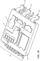
FIG. 1B is an isometric view of the power module ofFIG. 1A ; -
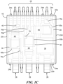
FIG. 1C is a plan view of the power module ofFIG. 1A ; -
FIG. 2A is a side view of another power module according to the disclosure and including a jumper; -
FIG. 2B is an isometric view of the power module ofFIG. 2A ; -
FIG. 2C is a plan view of the power module ofFIG. 2A ; -
FIG. 3A is an isometric view of a lead fame of the power modules ofFIGs. 1A-1C and2A-2C . -
FIG. 3B is an isometric view of the lead frame ofFIG. 3A after overmolding and plating; and -
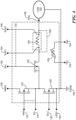
FIG. 4 is a schematic of the power modules ofFIGs. 1A-1C and2A-2C . - Referring to
FIGs. 1A ,1B , and1C , apower module 10 includes alead frame 50, one or moreelectrical components 65, and amold material 15 enclosing the electrical component. Thelead frame 50 includes at least onesignal lead 25, at least onepower lead 28, and apaddle 30 attached to one or more of the signal lead and the power lead. Theelectrical component 65 is supported by thepaddle 30. Internal to the module, electrical connection between leads and electrical components can be made in various ways, such as byclips 40 and/or bywire bonds 70. - According to an aspect of the disclosure, the
mold material 15 is configured to enclose a portion of thelead frame 50 and expose asurface 32 of thepaddle 30 such thatpower lead 28 has afirst portion 34 extending from an edge, orside surface 15a of the mold material outside of the mold material in a first direction (i.e., generally upward in the view ofFIG. 1A ) and asecond portion 36 enclosed by themold material 15 and extending from the edge of the mold material inside the mold material in a second direction (i.e., generally downward the view ofFIG. 1A ) to thepaddle 30, wherein the second direction is substantially opposite to the first direction. The first and second directions in which thepower lead portions module 10 as illustrated. -
Mold material 15 can be considered to form apackage 15 from which thesecond portion 36 of the leads extend to permit electrical connection to other circuits and systems (not shown). Leads 25, 28 are surface mount leads configured to be attached to bond pads of a printed circuit board or other suitable substrate in use. It will be appreciated that in use, themodule 10 can be inverted with respect to the view ofFIGs. 1A-1C and mounted with the orientation shown in the view ofFIG. 3B . - The first and
second portions power lead 28 can be considered to meet at ajunction 48. The exposedpaddle surface 32 can be referred to as a down set paddle portion or surface. Thelead 28 has ajog 38 between thejunction 48 and the down setpaddle surface 32, as shown. In embodiments, the down set height (jog height) can have a minimum dimension on the order of 1.0mm.Mold material 15 has afirst surface 15b and asecond surface 15c parallel to the first surface andside surface 15a extends from thefirst surface 15b to thesecond surface 15c. - With this arrangement of the first
power lead portion 34 extending in a different, substantially vertical direction than the secondpower lead portion 36, which second power lead portion extends to the down set exposedsurface 32 of thepaddle 30, a heatsink (or other direct contact heat conduction cooling system) 18 attached to the exposedpaddle surface 32 can be larger than otherwise possible. This is because theheatsink 18 can extend horizontally beyond theleads heat sink 18 for the module. By contrast, in conventional configurations in which the leads extend outside of the package in the same direction as the down setpaddle surface 32, the heatsink is confined to a width generally no larger than the width of themold material 15. - Referring also to
FIG. 3A ,lead frame 50 is shown in an orientation inverted with respect toFIGs. 1A-1C .FIG. 3B shows themodule 10 overmolded bymold material 15. From these views, down set exposedpaddle surface 32 can be seen. While lead features are explained in connection withpower lead 28 to includeportions junction 48, paddle 30 with down set exposedsurface 32,jog 38, etc., it will be appreciated that other leads (other power leads 28 and/or signal leads 25) can have similar features. In general, the down set area of some leads includes apaddle 30 supporting an electrical component and the down set area of other leads includes a bond pad for internal connection by aclip 40 orwire bond 70. Further, the down set area of still other leads may or may not be internally coupled in which case such "dummy leads" can form tie bars as will be explained. In general, as illustrated inFIG. 3B , the down set area of theleads - According to a further aspect, at least one
signal lead 25 and/orpower lead 28 has a recessed, or thinnedportion 42 enclosed by themold material 15 and configured to securely lock the respective lead into a fixed position relative to the mold material. The recessedportion 42 can be seen at various locations in the view ofFIG. 1B andFIG. 3A as labelled 42. Recessedportions 42 can be formed by various techniques including, but not limited to etching (by either wet etch or dry etch), stamping, coining or laser cutting. Formation of the recessed portion can reduce a thickness of the respective lead by about 40% to 60% and in some embodiments by about 50%. Themold material 15 engages the recessedportions 42 to form a locking mechanism by which the leads are firmly and fixedly held in place with respect to the mold material. Suitable materials for themold material 15 include thermoset and thermoplastic mold compounds and other commercially available IC mold compounds. In some embodiments, a recessedportion 42 is provided for those leads having a down set area with an exposed surface or having a down set paddle with an exposed surface, as shown inFIG. 3A . - An example circuit formed by the components within the
module 10 is shown and described in connection withFIG. 4 . Suffice it to say here that integratedelectrical component 65 can take various forms, such as a MOSFET. Here,power module 10 is shown to include threeFETs power module 10 can be referred to interchangeably as a multichip module. It will be appreciated that in some embodiments, more than onecomponent 65a- 65c and in some cases all of thecomponents device 10 may be referred to as a power IC rather than a power module. However, more generally, power IC and power module are used interchangeably. - Each FET supporting die is in turn attached to a
respective paddle 30. Various materials and techniques can be used to attach the die to the paddles, such as by soldering or with the use of an epoxy (either conductive or non-conductive epoxy may be used depending on the need) or an adhesive tape or sintered silver. - In addition to
power components 65a-65c, one or morepassive components 45 can be coupled between at least two signal leads within thepackage 15. For example, athermistor 45 can be coupled between signal leads 25, as shown.Thermistor 45 can monitor the internal temperature of the module and provide temperature information to an external controller. Other example passive components that can be integrated in a similar fashion include but are not limited to a resistor, a capacitor, inductor, a thermistor, or a diode. - Another example electrical component can be provided in the form of a shunt resistor, or simply shunt 35.
Shunt 35 can be coupled between apower lead 28, asignal lead 25, and a paddle as shown. -
Passive component 45 and shunt 35 can be attached to the down set area of one or more respective leads by soldering to one or more bond pads or with a conductive epoxy process as examples. - In general, signal leads 25 differ from power leads 28 in the types of signals carried, with power leads generally carrying higher power signals than signal leads. Accordingly, signal leads 25 tend to be smaller in width than power leads 28 as shown. In embodiments, a width of one or more signal leads 25 can be enlarged at a
bend area 25a (FIG. 1B ) of the lead in order to improve the lead's coplanarity, and positioning of leads with respect tomold body 15. - According to a further aspect, one or
more paddles 30 is only attached to thesecond portion 36 of the power lead (i.e., is only attached on one side) such that the paddle is cantilevered as shown. Stated differently, the down setpaddle surface 32 can be described as a one-sided down set. With this arrangement, stress that could otherwise occur due to the deep down set of the relatively thick lead frame is avoided and the required electrical isolation between the signal leads and power leads is achieved. - As shown in the plan view of
FIG. 1C ,package 15 has first and second opposingedges edges lead frame 50 includes at least one tie bar 24 (and here fivetie bars edges - As is apparent, the
bars 24a - 24e may or may not be connected within themodule 10. For example,tie bar 24a is electrically connected toelectrical component 65a and tie bars 24b and 24c are electrically connected toelectrical component 65c. Tie bars 24d and 24e however are not connected within thepackage 15 and thus, can be referred to as dummy leads or dummy tie bars. It will be appreciated that a paddle can be attached to a dummy lead (in addition to or instead of being attached one or more of a signal lead and a power lead). - With this arrangement of having tie bars that extend only from the package edges 22a, 22b from which the leads extend (rather than also or alternatively having tie bars extending from orthogonal packages edges 22c, 22d), the lead frame density is increased. Stated differently, the number of lead frame units that can be provided by the same area of lead frame metal is increased since "side protrusions" are avoided.
- The
junction 48 between thefirst lead portion 34 and the second lead portion 36 (i.e., the location at which thelead 28 exits thepackage 15 and thus the location where thefirst lead portion 34 starts andsecond lead portion 36 ends or vice versa) can be located at a parting, or separation line 90 (FIG. 3B ) in themold material 15 between afirst mold portion 16a and asecond mold portion 16b. In embodiments, thejunction 48 is located at a height of approximately one-fifth to one-third of a height of theside surface 15a of themold material 15, for example, thejunction 48 can be located at a height of approximately one-fourth of the height of theside surface 15a of themold material 15. - With this arrangement of the
lead 28 exiting thepackage 15 at theseparation line 90 between the first andsecond mold portions mold material 15 and thus, provides an improved strength of retention of the leads relative to thepackage 15. - During manufacture,
lead frame 50 is formed from a sheet or strip of metal that is patterned (e.g., stamped, etched) to provide the desired lead frame features (e.g., signal leads, power leads, and paddles) and the desired bends (e.g., jog 38, surface mount pads) in the leads. Generally, a plurality of lead frames likelead frame 50 are formed from the same metal sheet and tie bars hold together thelead frame 50 with other lead frames (not shown). Once themodule 10 is formed (i.e., once theelectrical component 65 is attached, internal electrical connections are made (e.g., by wire bonds or clips), and the device is overmolded by mold material 15), themodule 10 is separated (i.e., singulated) from other modules (not shown) formed from the same lead frame material. The thickness of the lead frame can vary. In some embodiments the lead frame thickness is on the order of 20 mils. As one example, the manufacturing process can include attaching the FET supporting die torespective paddles 30, attaching other components to paddles (e.g.,passives 45 and shunt 35), solder reflow to attach the die and other components to bond pads on the paddles, attachingclips 40, another solder reflow, and attachingwire bonds 70. The subassembly thus formed can then be overmolded withmold material 15. -
Mold material 15 can be formed by a single step molding process by which thefirst mold portion 16a and thesecond mold portion 16b are formed. For example, the lead frame subassembly (i.e.,lead frame 50 with components and interconnections in place) can be placed in a hollow space created by joining the two mold cavities (i.e., negatives) that can be held together by means of high-pressure hydraulic systems. Molding compound is then forced through a small opening (i.e., gate) into the cavities by a process such as injection molding, compression molding, transfer molding, or potting. After sufficient time has passed, the mold material is partially cured and then the two mold chases are separated, and the molded body is then "ejected" out of the cavities. The molded body unit is then fully cured at high temperature to improved mechanical strength of the molded body. - Referring also to
FIGs. 2A ,2B , and2C , apower module 200 is shown which is similar to themodule 10 ofFIGs. 1A ,1B , and1C .Module 200 differs frommodule 10 only in thatshunt 35 is replaced with ajumper 44. Thus, like elements with respect toFIGs. 1A ,1B , and1C are labeled with like reference numbers. - Referring also to
FIG. 4 , a schematic representation of amodule 110 is shown, whichmodule 110 can be the same as or similar tomodule 10 ofFIGs. 1A-1C ormodule 200 ofFIGs. 2A-2C . In order to provide themodule 10 ofFIGs. 1A-1C ,module 110 includes a shunt resistor or simply ashunt 160 as may be the same as or similar to shunt 35 ofFIGs. 1A-1C .Shunt 160 can be used to sense a load current (i.e., a motor phase current). To this end, leadsSUS1 154 andSUS2 156 permit external connection to terminals of the shunt, as shown. In order to providemodule 200 ofFIGs. 2A-2C ,module 110 includes jumper 44 (shown schematically bydotted line 168 inFIG. 4 ) instead of theshunt 160. Becausemodules module 110 requiring just a simple change of replacing theshunt 160 with thejumper 168 or vice versa, the manufacturing expense (e.g., tooling costs) of providingmodules -
Module 110 includesFETs FETs FETs lead VBRG 135 coupled to a drain terminal ofFET 130, leadGHU 132 coupled to a gate terminal ofFET 130, lead SU 134 coupled to a source terminal ofFET 130, leadGLU 142 coupled to a gate terminal ofFET 140, leadLSSU 144 coupled to a source terminal ofFET 140, and leadGIU 152 coupled to a gate terminal ofFET 150. Also shown in the schematic ofFIG. 4 isthermistor 165 that can be the same as or similar to thermistor 45 (FIGs. 1B-1C ,2B-2C ).FET 150 can be coupled to aload 120 as can take various forms depending on the application. In some embodiments, theload 120 is a motor winding. LeadsVBRG 135,PHU 158, andPGND 166 can be power leads 28 and the remaining leads can be signal leads. - According to an aspect of the disclosure, at least one FET has an additional connection to its source terminal for diagnostic purposes. In particular, generally FETs require only one external connection to a gate terminal to operate. Here, FET 140 (i.e.,
FET 65b inFIGs. 1A-1C ,2A-2C ) has an additional external connection to its source terminal provided bylead LSSU 144. LeadLSSU 144 is coupled to a source bond pad (labelled 72 inFIGs. 1B ,1C ,2B ,2C ) on theFET 140 by awire bond 70d. This arrangement is advantageous for testing purposes, such as in order to meet the high safety standards for certain types of applications such as Automotive Safety Integrity Level (ASIL) requirements. Without this extrasource bond pad 72, in order to electrically connect to the source ofFET 140, wire would have been bonded to acopper clip 40 which would require additional plating thus increasing design and production costs. - Internal to the module, electrical connection between leads and internal components can be made in various ways, such as by
clips 40 or bywire bonds 70. For example, connection between a transistor gate terminal and a signal lead can be made by wire bonds, as labelledwire bonds FIGs. 1C and2C forFETs bond pad 72 as shown inFIGs. 1C ,2C . - It will be appreciated that the particular components and circuits shown in the figures are examples and the various advantageous features described herein can be applied to other component and circuit combinations. By way of one non-limiting example, a module according to the disclosure can be provided for controlling three phases of a motor instead of a single phase as shown in
FIG. 4 . To this end, such a module can contain nine FETs (rather than the three illustrated inFIG. 4 ), with three such FETs controlling each phase of a three-phase motor.
Claims (15)
- A power integrated circuit (IC) (10) comprising:a lead frame (50) comprising a signal lead (25), a power lead (28), a tie bar (24a, 24b, 24c, 24d, 24e), and a paddle (30), wherein the paddle is attached to one or more of the signal lead and the power lead;an electrical component (65) supported by the paddle; anda mold material (15) configured to enclose a portion of the lead frame and expose a surface of the paddle, wherein the power lead has a first portion extending from an edge of the mold material outside of the mold material in a first direction and a second portion enclosed by the mold material and extending from the edge of the mold material inside the mold material in a second direction to the paddle, wherein the second direction is substantially opposite to the first direction; andwherein the mold material (15) forms an IC package having first and second opposing edges (22a, 22b) from which the signal lead (25) and the power lead (28) extend and having third and fourth opposing edges (22c, 22d) orthogonal to the first and second opposing edges (22a, 22b), and wherein the tie bar extends from one of the first or second opposing edges (22a, 22b) and does not extend from the third or fourth opposing edges (22c, 22d).
- The power IC of claim 1 wherein the lead frame further comprises a dummy lead and wherein the paddle is attached to one or more of the signal lead, the power lead, and the dummy lead.
- The power IC of claim 1 wherein the paddle is only attached to the second portion of the power lead.
- The power IC of claim 1 wherein the mold material has a first surface, a second surface positioned parallel to the first surface, and a side surface extending from the first surface to the second surface, wherein the first and second portions of the power lead meet at a junction between a first portion of the mold material and a second portion of the mold material positioned at the side surface of the mold material.
- The power IC of claim 4 wherein the junction is located at a height of approximately one-fifth to one-third of a height of the side surface of the mold material.
- The power IC of claim 5 wherein the junction is located at a height of approximately one-fourth of the height of the side surface of the mold material.
- The power IC of claim 1 wherein at least one of the signal lead and the power lead has a recessed portion enclosed by the mold material and configured to lock the at least one lead into a fixed position relative to the exposed surface of the paddle.
- The power IC of claim 7 wherein the recessed portion of the at least one lead is formed by etching, stamping, coining, or laser cutting.
- The power IC of claim 1 wherein the exposed surface of the paddle is configured to attach to a heatsink configured to extend beyond a surface of the mold material.
- The power IC of claim 1 further comprising at least one passive component coupled between at least two signal leads and enclosed by the mold material.
- The power IC of claim 10 wherein the passive component comprises one or more of a resistor, a capacitor, an inductor, a thermistor, or a diode.
- The power IC of claim 1 wherein the lead frame comprises a plurality of signal leads, a plurality of power leads, and a plurality of paddles each attached to a respective one of the plurality of power leads or the plurality of signal leads, wherein the electrical component comprises a plurality of Field Effect Transistors (FETs) each supported by a respective paddle and electrically coupled to form a half H-bridge.
- The power IC of claim 12 wherein at least one of the plurality of FETs comprises a source terminal located external to the mold material and accessible at one of the plurality of signal leads.
- The power IC of claim 13 further comprising any one of:a wire bond extending from the one of the plurality of signal leads to a bond pad coupled to a source terminal of at least one FET;a shunt coupled between the signal lead, the power lead, and the paddle; anda jumper coupled in series with the power lead.
- The power IC of claim 1 wherein the signal lead comprises a first width at an end configured for external coupling and a second width larger than the first width at a bend.
Applications Claiming Priority (2)
| Application Number | Priority Date | Filing Date | Title |
|---|---|---|---|
| US16/746,275 US11183436B2 (en) | 2020-01-17 | 2020-01-17 | Power module package and packaging techniques |
| PCT/US2020/065949 WO2021146027A1 (en) | 2020-01-17 | 2020-12-18 | Power module package and packaging techniques |
Publications (2)
| Publication Number | Publication Date |
|---|---|
| EP4062446A1 EP4062446A1 (en) | 2022-09-28 |
| EP4062446B1 true EP4062446B1 (en) | 2024-12-11 |
Family
ID=74195118
Family Applications (1)
| Application Number | Title | Priority Date | Filing Date |
|---|---|---|---|
| EP20845268.0A Active EP4062446B1 (en) | 2020-01-17 | 2020-12-18 | Power module package |
Country Status (4)
| Country | Link |
|---|---|
| US (1) | US11183436B2 (en) |
| EP (1) | EP4062446B1 (en) |
| KR (1) | KR102826659B1 (en) |
| WO (1) | WO2021146027A1 (en) |
Families Citing this family (7)
| Publication number | Priority date | Publication date | Assignee | Title |
|---|---|---|---|---|
| US11150273B2 (en) | 2020-01-17 | 2021-10-19 | Allegro Microsystems, Llc | Current sensor integrated circuits |
| USD1073632S1 (en) * | 2021-04-23 | 2025-05-06 | Wolfspeed, Inc. | Power module |
| US12487254B2 (en) | 2021-08-23 | 2025-12-02 | Allegro Microsystems, Llc | Packaged current sensor integrated circuit |
| CN116093091A (en) * | 2021-11-02 | 2023-05-09 | 立锜科技股份有限公司 | Heat radiation structure and high heat transfer element |
| JP7609046B2 (en) * | 2021-12-07 | 2025-01-07 | 三菱電機株式会社 | Semiconductor Device |
| US12557668B2 (en) | 2023-04-27 | 2026-02-17 | Allegro Microsystems, Llc | High voltage integrated circuit packages with diagonalized lead configuration and method of making the same |
| US12493057B2 (en) | 2023-11-17 | 2025-12-09 | Allegro Microsystems, Llc | Current sensor integrated circuit |
Family Cites Families (36)
| Publication number | Priority date | Publication date | Assignee | Title |
|---|---|---|---|---|
| JP2708191B2 (en) * | 1988-09-20 | 1998-02-04 | 株式会社日立製作所 | Semiconductor device |
| KR100333386B1 (en) * | 1999-06-29 | 2002-04-18 | 박종섭 | chip scale package |
| US7042068B2 (en) * | 2000-04-27 | 2006-05-09 | Amkor Technology, Inc. | Leadframe and semiconductor package made using the leadframe |
| US6630726B1 (en) * | 2001-11-07 | 2003-10-07 | Amkor Technology, Inc. | Power semiconductor package with strap |
| US20040080028A1 (en) * | 2002-09-05 | 2004-04-29 | Kabushiki Kaisha Toshiba | Semiconductor device with semiconductor chip mounted in package |
| US7709754B2 (en) | 2003-08-26 | 2010-05-04 | Allegro Microsystems, Inc. | Current sensor |
| US20100253435A1 (en) * | 2004-03-18 | 2010-10-07 | Ikuroh Ichitsubo | Rf power amplifier circuit utilizing bondwires in impedance matching |
| US7768083B2 (en) | 2006-01-20 | 2010-08-03 | Allegro Microsystems, Inc. | Arrangements for an integrated sensor |
| DE102006021959B4 (en) | 2006-05-10 | 2011-12-29 | Infineon Technologies Ag | Power semiconductor device and method for its production |
| US20080013298A1 (en) | 2006-07-14 | 2008-01-17 | Nirmal Sharma | Methods and apparatus for passive attachment of components for integrated circuits |
| US8422243B2 (en) * | 2006-12-13 | 2013-04-16 | Stats Chippac Ltd. | Integrated circuit package system employing a support structure with a recess |
| US8124461B2 (en) * | 2006-12-27 | 2012-02-28 | Mediatek Inc. | Method for manufacturing leadframe, packaging method for using the leadframe and semiconductor package product |
| US20090127677A1 (en) | 2007-11-21 | 2009-05-21 | Gomez Jocel P | Multi-Terminal Package Assembly For Semiconductor Devices |
| US20100164078A1 (en) * | 2008-12-31 | 2010-07-01 | Ruben Madrid | Package assembly for semiconductor devices |
| US9659845B2 (en) * | 2010-12-13 | 2017-05-23 | Infineon Technologies Americas Corp. | Power quad flat no-lead (PQFN) package in a single shunt inverter circuit |
| JP5936310B2 (en) | 2011-03-17 | 2016-06-22 | 三菱電機株式会社 | Power semiconductor module and its mounting structure |
| US9812588B2 (en) | 2012-03-20 | 2017-11-07 | Allegro Microsystems, Llc | Magnetic field sensor integrated circuit with integral ferromagnetic material |
| US10234513B2 (en) | 2012-03-20 | 2019-03-19 | Allegro Microsystems, Llc | Magnetic field sensor integrated circuit with integral ferromagnetic material |
| US9494660B2 (en) | 2012-03-20 | 2016-11-15 | Allegro Microsystems, Llc | Integrated circuit package having a split lead frame |
| US9666788B2 (en) | 2012-03-20 | 2017-05-30 | Allegro Microsystems, Llc | Integrated circuit package having a split lead frame |
| US10271448B2 (en) * | 2012-08-06 | 2019-04-23 | Investar Corporation | Thin leadframe QFN package design of RF front-ends for mobile wireless communication |
| US20140070329A1 (en) * | 2012-09-07 | 2014-03-13 | Fairchild Semiconductor Corporation | Wireless module with active and passive components |
| US9035435B2 (en) | 2012-11-14 | 2015-05-19 | Power Integrations, Inc. | Magnetically coupled galvanically isolated communication using lead frame |
| US8976561B2 (en) | 2012-11-14 | 2015-03-10 | Power Integrations, Inc. | Switch mode power converters using magnetically coupled galvanically isolated lead frame communication |
| US9190606B2 (en) | 2013-03-15 | 2015-11-17 | Allegro Micosystems, LLC | Packaging for an electronic device |
| US10345343B2 (en) | 2013-03-15 | 2019-07-09 | Allegro Microsystems, Llc | Current sensor isolation |
| US9411025B2 (en) | 2013-04-26 | 2016-08-09 | Allegro Microsystems, Llc | Integrated circuit package having a split lead frame and a magnet |
| DE102015101674B4 (en) | 2015-02-05 | 2021-04-29 | Infineon Technologies Austria Ag | Semiconductor chip housing with contact pins on short side edges |
| US10168391B2 (en) | 2015-06-23 | 2019-01-01 | Infineon Technologies Ag | Multi-functional interconnect module and carrier with multi-functional interconnect module attached thereto |
| DE102015122259B4 (en) * | 2015-12-18 | 2020-12-24 | Infineon Technologies Austria Ag | Semiconductor devices having a porous insulating layer |
| US9716057B1 (en) | 2016-08-24 | 2017-07-25 | United Silicon Carbide, Inc. | Offset leadframe cascode package |
| DE102017202770B4 (en) * | 2016-08-31 | 2023-06-07 | Infineon Technologies Austria Ag | Semiconductor die package having a repeating footprint pattern |
| US9704789B1 (en) | 2016-10-16 | 2017-07-11 | Alpha And Omega Semiconductor (Cayman) Ltd. | Molded intelligent power module |
| US10481181B2 (en) | 2017-04-25 | 2019-11-19 | Allegro Microsystems, Llc | Systems and methods for current sensing |
| JP6843731B2 (en) | 2017-11-22 | 2021-03-17 | 三菱電機株式会社 | Semiconductor device |
| US10566713B2 (en) * | 2018-01-09 | 2020-02-18 | Semiconductor Components Industries, Llc | Press-fit power module and related methods |
-
2020
- 2020-01-17 US US16/746,275 patent/US11183436B2/en active Active
- 2020-12-18 EP EP20845268.0A patent/EP4062446B1/en active Active
- 2020-12-18 WO PCT/US2020/065949 patent/WO2021146027A1/en not_active Ceased
- 2020-12-18 KR KR1020227028105A patent/KR102826659B1/en active Active
Also Published As
| Publication number | Publication date |
|---|---|
| US11183436B2 (en) | 2021-11-23 |
| KR102826659B1 (en) | 2025-06-27 |
| EP4062446A1 (en) | 2022-09-28 |
| US20210225721A1 (en) | 2021-07-22 |
| WO2021146027A1 (en) | 2021-07-22 |
| KR20220129587A (en) | 2022-09-23 |
Similar Documents
| Publication | Publication Date | Title |
|---|---|---|
| US11183436B2 (en) | Power module package and packaging techniques | |
| CN110785838B (en) | Resin encapsulated power semiconductor module with exposed terminal area | |
| CN101681897B (en) | Double-sided cooling integrated power device package and module and method of manufacturing the same | |
| CN113016068B (en) | Semiconductor module, power conversion device and method for manufacturing semiconductor module | |
| US6307272B1 (en) | Semiconductor device and method for manufacturing the same | |
| US8093692B2 (en) | Semiconductor device packaging including a power semiconductor element | |
| EP2662892B1 (en) | Stacked interposer leadframes | |
| US11973012B2 (en) | Power module with semiconductor packages mounted on metal frame | |
| CN107004648A (en) | Heat dissipation substrate for mounting electronic component | |
| US20110278706A1 (en) | Power Electronic Device Package | |
| US20220189885A1 (en) | Packaged device carrier for thermal enhancement or signal redistribution of packaged semiconductor devices | |
| CN107799484A (en) | Semiconductor die package with the area of coverage mould repeated | |
| US20090127681A1 (en) | Semiconductor package and method of fabricating the same | |
| US11538742B2 (en) | Packaged multichip module with conductive connectors | |
| US8471370B2 (en) | Semiconductor element with semiconductor die and lead frames | |
| US20230361011A1 (en) | Molded power modules | |
| US20240021496A1 (en) | Semiconductor device | |
| CN112582386B (en) | Power module, preparation method thereof and electrical equipment | |
| US6979900B2 (en) | Integrated circuit package with integral leadframe convector and method therefor | |
| CN117012743A (en) | electronic components | |
| JP2026510973A (en) | Semiconductor package design with a top-side heat spreader and bottom-side flat leads. | |
| CN112435972A (en) | Power module, preparation method thereof and electrical equipment |
Legal Events
| Date | Code | Title | Description |
|---|---|---|---|
| STAA | Information on the status of an ep patent application or granted ep patent |
Free format text: STATUS: UNKNOWN |
|
| STAA | Information on the status of an ep patent application or granted ep patent |
Free format text: STATUS: THE INTERNATIONAL PUBLICATION HAS BEEN MADE |
|
| PUAI | Public reference made under article 153(3) epc to a published international application that has entered the european phase |
Free format text: ORIGINAL CODE: 0009012 |
|
| STAA | Information on the status of an ep patent application or granted ep patent |
Free format text: STATUS: REQUEST FOR EXAMINATION WAS MADE |
|
| 17P | Request for examination filed |
Effective date: 20220621 |
|
| AK | Designated contracting states |
Kind code of ref document: A1 Designated state(s): AL AT BE BG CH CY CZ DE DK EE ES FI FR GB GR HR HU IE IS IT LI LT LU LV MC MK MT NL NO PL PT RO RS SE SI SK SM TR |
|
| DAV | Request for validation of the european patent (deleted) | ||
| DAX | Request for extension of the european patent (deleted) | ||
| GRAP | Despatch of communication of intention to grant a patent |
Free format text: ORIGINAL CODE: EPIDOSNIGR1 |
|
| STAA | Information on the status of an ep patent application or granted ep patent |
Free format text: STATUS: GRANT OF PATENT IS INTENDED |
|
| INTG | Intention to grant announced |
Effective date: 20240719 |
|
| GRAS | Grant fee paid |
Free format text: ORIGINAL CODE: EPIDOSNIGR3 |
|
| GRAA | (expected) grant |
Free format text: ORIGINAL CODE: 0009210 |
|
| STAA | Information on the status of an ep patent application or granted ep patent |
Free format text: STATUS: THE PATENT HAS BEEN GRANTED |
|
| AK | Designated contracting states |
Kind code of ref document: B1 Designated state(s): AL AT BE BG CH CY CZ DE DK EE ES FI FR GB GR HR HU IE IS IT LI LT LU LV MC MK MT NL NO PL PT RO RS SE SI SK SM TR |
|
| REG | Reference to a national code |
Ref country code: GB Ref legal event code: FG4D |
|
| REG | Reference to a national code |
Ref country code: CH Ref legal event code: EP |
|
| REG | Reference to a national code |
Ref country code: DE Ref legal event code: R096 Ref document number: 602020043094 Country of ref document: DE |
|
| REG | Reference to a national code |
Ref country code: IE Ref legal event code: FG4D |
|
| REG | Reference to a national code |
Ref country code: LT Ref legal event code: MG9D |
|
| PG25 | Lapsed in a contracting state [announced via postgrant information from national office to epo] |
Ref country code: HR Free format text: LAPSE BECAUSE OF FAILURE TO SUBMIT A TRANSLATION OF THE DESCRIPTION OR TO PAY THE FEE WITHIN THE PRESCRIBED TIME-LIMIT Effective date: 20241211 |
|
| PG25 | Lapsed in a contracting state [announced via postgrant information from national office to epo] |
Ref country code: FI Free format text: LAPSE BECAUSE OF FAILURE TO SUBMIT A TRANSLATION OF THE DESCRIPTION OR TO PAY THE FEE WITHIN THE PRESCRIBED TIME-LIMIT Effective date: 20241211 |
|
| PG25 | Lapsed in a contracting state [announced via postgrant information from national office to epo] |
Ref country code: BG Free format text: LAPSE BECAUSE OF FAILURE TO SUBMIT A TRANSLATION OF THE DESCRIPTION OR TO PAY THE FEE WITHIN THE PRESCRIBED TIME-LIMIT Effective date: 20241211 |
|
| REG | Reference to a national code |
Ref country code: NL Ref legal event code: MP Effective date: 20241211 |
|
| PG25 | Lapsed in a contracting state [announced via postgrant information from national office to epo] |
Ref country code: ES Free format text: LAPSE BECAUSE OF FAILURE TO SUBMIT A TRANSLATION OF THE DESCRIPTION OR TO PAY THE FEE WITHIN THE PRESCRIBED TIME-LIMIT Effective date: 20241211 |
|
| PG25 | Lapsed in a contracting state [announced via postgrant information from national office to epo] |
Ref country code: NO Free format text: LAPSE BECAUSE OF FAILURE TO SUBMIT A TRANSLATION OF THE DESCRIPTION OR TO PAY THE FEE WITHIN THE PRESCRIBED TIME-LIMIT Effective date: 20250311 |
|
| PG25 | Lapsed in a contracting state [announced via postgrant information from national office to epo] |
Ref country code: GR Free format text: LAPSE BECAUSE OF FAILURE TO SUBMIT A TRANSLATION OF THE DESCRIPTION OR TO PAY THE FEE WITHIN THE PRESCRIBED TIME-LIMIT Effective date: 20250312 Ref country code: LV Free format text: LAPSE BECAUSE OF FAILURE TO SUBMIT A TRANSLATION OF THE DESCRIPTION OR TO PAY THE FEE WITHIN THE PRESCRIBED TIME-LIMIT Effective date: 20241211 |
|
| PG25 | Lapsed in a contracting state [announced via postgrant information from national office to epo] |
Ref country code: RS Free format text: LAPSE BECAUSE OF FAILURE TO SUBMIT A TRANSLATION OF THE DESCRIPTION OR TO PAY THE FEE WITHIN THE PRESCRIBED TIME-LIMIT Effective date: 20250311 |
|
| PG25 | Lapsed in a contracting state [announced via postgrant information from national office to epo] |
Ref country code: NL Free format text: LAPSE BECAUSE OF FAILURE TO SUBMIT A TRANSLATION OF THE DESCRIPTION OR TO PAY THE FEE WITHIN THE PRESCRIBED TIME-LIMIT Effective date: 20241211 |
|
| REG | Reference to a national code |
Ref country code: AT Ref legal event code: MK05 Ref document number: 1751085 Country of ref document: AT Kind code of ref document: T Effective date: 20241211 |
|
| PG25 | Lapsed in a contracting state [announced via postgrant information from national office to epo] |
Ref country code: SM Free format text: LAPSE BECAUSE OF FAILURE TO SUBMIT A TRANSLATION OF THE DESCRIPTION OR TO PAY THE FEE WITHIN THE PRESCRIBED TIME-LIMIT Effective date: 20241211 |
|
| PG25 | Lapsed in a contracting state [announced via postgrant information from national office to epo] |
Ref country code: PL Free format text: LAPSE BECAUSE OF FAILURE TO SUBMIT A TRANSLATION OF THE DESCRIPTION OR TO PAY THE FEE WITHIN THE PRESCRIBED TIME-LIMIT Effective date: 20241211 |
|
| PG25 | Lapsed in a contracting state [announced via postgrant information from national office to epo] |
Ref country code: IS Free format text: LAPSE BECAUSE OF FAILURE TO SUBMIT A TRANSLATION OF THE DESCRIPTION OR TO PAY THE FEE WITHIN THE PRESCRIBED TIME-LIMIT Effective date: 20250411 |
|
| PG25 | Lapsed in a contracting state [announced via postgrant information from national office to epo] |
Ref country code: PT Free format text: LAPSE BECAUSE OF FAILURE TO SUBMIT A TRANSLATION OF THE DESCRIPTION OR TO PAY THE FEE WITHIN THE PRESCRIBED TIME-LIMIT Effective date: 20250411 |
|
| PG25 | Lapsed in a contracting state [announced via postgrant information from national office to epo] |
Ref country code: EE Free format text: LAPSE BECAUSE OF FAILURE TO SUBMIT A TRANSLATION OF THE DESCRIPTION OR TO PAY THE FEE WITHIN THE PRESCRIBED TIME-LIMIT Effective date: 20241211 |
|
| PG25 | Lapsed in a contracting state [announced via postgrant information from national office to epo] |
Ref country code: RO Free format text: LAPSE BECAUSE OF FAILURE TO SUBMIT A TRANSLATION OF THE DESCRIPTION OR TO PAY THE FEE WITHIN THE PRESCRIBED TIME-LIMIT Effective date: 20241211 Ref country code: AT Free format text: LAPSE BECAUSE OF FAILURE TO SUBMIT A TRANSLATION OF THE DESCRIPTION OR TO PAY THE FEE WITHIN THE PRESCRIBED TIME-LIMIT Effective date: 20241211 |
|
| PG25 | Lapsed in a contracting state [announced via postgrant information from national office to epo] |
Ref country code: SK Free format text: LAPSE BECAUSE OF FAILURE TO SUBMIT A TRANSLATION OF THE DESCRIPTION OR TO PAY THE FEE WITHIN THE PRESCRIBED TIME-LIMIT Effective date: 20241211 |
|
| PG25 | Lapsed in a contracting state [announced via postgrant information from national office to epo] |
Ref country code: CZ Free format text: LAPSE BECAUSE OF FAILURE TO SUBMIT A TRANSLATION OF THE DESCRIPTION OR TO PAY THE FEE WITHIN THE PRESCRIBED TIME-LIMIT Effective date: 20241211 |
|
| PG25 | Lapsed in a contracting state [announced via postgrant information from national office to epo] |
Ref country code: IT Free format text: LAPSE BECAUSE OF FAILURE TO SUBMIT A TRANSLATION OF THE DESCRIPTION OR TO PAY THE FEE WITHIN THE PRESCRIBED TIME-LIMIT Effective date: 20241211 |
|
| REG | Reference to a national code |
Ref country code: CH Ref legal event code: PL |
|
| PG25 | Lapsed in a contracting state [announced via postgrant information from national office to epo] |
Ref country code: LU Free format text: LAPSE BECAUSE OF NON-PAYMENT OF DUE FEES Effective date: 20241218 |
|
| PG25 | Lapsed in a contracting state [announced via postgrant information from national office to epo] |
Ref country code: SE Free format text: LAPSE BECAUSE OF FAILURE TO SUBMIT A TRANSLATION OF THE DESCRIPTION OR TO PAY THE FEE WITHIN THE PRESCRIBED TIME-LIMIT Effective date: 20241211 |
|
| REG | Reference to a national code |
Ref country code: DE Ref legal event code: R097 Ref document number: 602020043094 Country of ref document: DE |
|
| PG25 | Lapsed in a contracting state [announced via postgrant information from national office to epo] |
Ref country code: MC Free format text: LAPSE BECAUSE OF FAILURE TO SUBMIT A TRANSLATION OF THE DESCRIPTION OR TO PAY THE FEE WITHIN THE PRESCRIBED TIME-LIMIT Effective date: 20241211 |
|
| REG | Reference to a national code |
Ref country code: BE Ref legal event code: MM Effective date: 20241231 |
|
| PG25 | Lapsed in a contracting state [announced via postgrant information from national office to epo] |
Ref country code: DK Free format text: LAPSE BECAUSE OF FAILURE TO SUBMIT A TRANSLATION OF THE DESCRIPTION OR TO PAY THE FEE WITHIN THE PRESCRIBED TIME-LIMIT Effective date: 20241211 |
|
| PG25 | Lapsed in a contracting state [announced via postgrant information from national office to epo] |
Ref country code: BE Free format text: LAPSE BECAUSE OF NON-PAYMENT OF DUE FEES Effective date: 20241231 |
|
| PLBE | No opposition filed within time limit |
Free format text: ORIGINAL CODE: 0009261 |
|
| STAA | Information on the status of an ep patent application or granted ep patent |
Free format text: STATUS: NO OPPOSITION FILED WITHIN TIME LIMIT |
|
| PG25 | Lapsed in a contracting state [announced via postgrant information from national office to epo] |
Ref country code: CH Free format text: LAPSE BECAUSE OF NON-PAYMENT OF DUE FEES Effective date: 20241231 |
|
| PG25 | Lapsed in a contracting state [announced via postgrant information from national office to epo] |
Ref country code: IE Free format text: LAPSE BECAUSE OF NON-PAYMENT OF DUE FEES Effective date: 20241218 |
|
| 26N | No opposition filed |
Effective date: 20250912 |
|
| GBPC | Gb: european patent ceased through non-payment of renewal fee |
Effective date: 20250311 |
|
| REG | Reference to a national code |
Ref country code: DE Ref legal event code: R079 Ref document number: 602020043094 Country of ref document: DE Free format text: PREVIOUS MAIN CLASS: H01L0023360000 Ipc: H10W0040200000 |
|
| PGFP | Annual fee paid to national office [announced via postgrant information from national office to epo] |
Ref country code: DE Payment date: 20250930 Year of fee payment: 6 |
|
| PG25 | Lapsed in a contracting state [announced via postgrant information from national office to epo] |
Ref country code: GB Free format text: LAPSE BECAUSE OF NON-PAYMENT OF DUE FEES Effective date: 20250311 |
|
| PG25 | Lapsed in a contracting state [announced via postgrant information from national office to epo] |
Ref country code: FR Free format text: LAPSE BECAUSE OF NON-PAYMENT OF DUE FEES Effective date: 20250211 |
|
| PG25 | Lapsed in a contracting state [announced via postgrant information from national office to epo] |
Ref country code: CY Free format text: LAPSE BECAUSE OF FAILURE TO SUBMIT A TRANSLATION OF THE DESCRIPTION OR TO PAY THE FEE WITHIN THE PRESCRIBED TIME-LIMIT Effective date: 20241211 |