EP4053907A1 - Display substrate and display device - Google Patents
Display substrate and display device Download PDFInfo
- Publication number
- EP4053907A1 EP4053907A1 EP21832137.0A EP21832137A EP4053907A1 EP 4053907 A1 EP4053907 A1 EP 4053907A1 EP 21832137 A EP21832137 A EP 21832137A EP 4053907 A1 EP4053907 A1 EP 4053907A1
- Authority
- EP
- European Patent Office
- Prior art keywords
- pixel
- sub
- line
- signal line
- pixel groups
- Prior art date
- Legal status (The legal status is an assumption and is not a legal conclusion. Google has not performed a legal analysis and makes no representation as to the accuracy of the status listed.)
- Granted
Links
Images
Classifications
-
- H—ELECTRICITY
- H10—SEMICONDUCTOR DEVICES; ELECTRIC SOLID-STATE DEVICES NOT OTHERWISE PROVIDED FOR
- H10K—ORGANIC ELECTRIC SOLID-STATE DEVICES
- H10K59/00—Integrated devices, or assemblies of multiple devices, comprising at least one organic light-emitting element covered by group H10K50/00
- H10K59/30—Devices specially adapted for multicolour light emission
- H10K59/35—Devices specially adapted for multicolour light emission comprising red-green-blue [RGB] subpixels
- H10K59/352—Devices specially adapted for multicolour light emission comprising red-green-blue [RGB] subpixels the areas of the RGB subpixels being different
-
- H—ELECTRICITY
- H10—SEMICONDUCTOR DEVICES; ELECTRIC SOLID-STATE DEVICES NOT OTHERWISE PROVIDED FOR
- H10K—ORGANIC ELECTRIC SOLID-STATE DEVICES
- H10K59/00—Integrated devices, or assemblies of multiple devices, comprising at least one organic light-emitting element covered by group H10K50/00
- H10K59/10—OLED displays
- H10K59/12—Active-matrix OLED [AMOLED] displays
- H10K59/126—Shielding, e.g. light-blocking means over the TFTs
-
- H—ELECTRICITY
- H10—SEMICONDUCTOR DEVICES; ELECTRIC SOLID-STATE DEVICES NOT OTHERWISE PROVIDED FOR
- H10K—ORGANIC ELECTRIC SOLID-STATE DEVICES
- H10K59/00—Integrated devices, or assemblies of multiple devices, comprising at least one organic light-emitting element covered by group H10K50/00
- H10K59/10—OLED displays
- H10K59/12—Active-matrix OLED [AMOLED] displays
- H10K59/131—Interconnections, e.g. wiring lines or terminals
-
- H—ELECTRICITY
- H10—SEMICONDUCTOR DEVICES; ELECTRIC SOLID-STATE DEVICES NOT OTHERWISE PROVIDED FOR
- H10K—ORGANIC ELECTRIC SOLID-STATE DEVICES
- H10K59/00—Integrated devices, or assemblies of multiple devices, comprising at least one organic light-emitting element covered by group H10K50/00
- H10K59/30—Devices specially adapted for multicolour light emission
- H10K59/35—Devices specially adapted for multicolour light emission comprising red-green-blue [RGB] subpixels
- H10K59/353—Devices specially adapted for multicolour light emission comprising red-green-blue [RGB] subpixels characterised by the geometrical arrangement of the RGB subpixels
-
- H—ELECTRICITY
- H10—SEMICONDUCTOR DEVICES; ELECTRIC SOLID-STATE DEVICES NOT OTHERWISE PROVIDED FOR
- H10K—ORGANIC ELECTRIC SOLID-STATE DEVICES
- H10K59/00—Integrated devices, or assemblies of multiple devices, comprising at least one organic light-emitting element covered by group H10K50/00
- H10K59/60—OLEDs integrated with inorganic light-sensitive elements, e.g. with inorganic solar cells or inorganic photodiodes
-
- H—ELECTRICITY
- H10—SEMICONDUCTOR DEVICES; ELECTRIC SOLID-STATE DEVICES NOT OTHERWISE PROVIDED FOR
- H10K—ORGANIC ELECTRIC SOLID-STATE DEVICES
- H10K59/00—Integrated devices, or assemblies of multiple devices, comprising at least one organic light-emitting element covered by group H10K50/00
- H10K59/60—OLEDs integrated with inorganic light-sensitive elements, e.g. with inorganic solar cells or inorganic photodiodes
- H10K59/65—OLEDs integrated with inorganic image sensors
-
- H—ELECTRICITY
- H10—SEMICONDUCTOR DEVICES; ELECTRIC SOLID-STATE DEVICES NOT OTHERWISE PROVIDED FOR
- H10K—ORGANIC ELECTRIC SOLID-STATE DEVICES
- H10K59/00—Integrated devices, or assemblies of multiple devices, comprising at least one organic light-emitting element covered by group H10K50/00
- H10K59/80—Constructional details
- H10K59/8791—Arrangements for improving contrast, e.g. preventing reflection of ambient light
- H10K59/8792—Arrangements for improving contrast, e.g. preventing reflection of ambient light comprising light absorbing layers, e.g. black layers
Definitions
- OLED organic light emitting diode
- the embodiments of the present disclosure provide a display substrate and a display device.
- the display substrate includes a base substrate including a first display region and a second display region, the second display region at least partially surrounding the first display region; and a plurality of sub-pixels located on the base substrate and in the first display region and the second display region, a density of the sub-pixels in the first display region is less than a density of the sub-pixels in the second display region, each sub-pixel includes a pixel circuit, the plurality of sub-pixels include a first sub-pixel, a second sub-pixel and a third sub-pixel, the plurality of sub-pixels include a plurality of first pixel groups and a plurality of second pixel groups, the plurality of first pixel groups are located in the first display region, the plurality of second pixel groups are located in the second display region, the first display region includes a plurality of sub-display regions and a sub-light-transmitting region between the sub-display regions, the plurality of first
- At least one embodiment of the present disclosure provides a display substrate, which includes: a base substrate, including a first display region and a second display region, the second display region at least partially surrounding the first display region; and a plurality of sub-pixels, located on the base substrate and in the first display region and the second display region, a density of the sub-pixels in the first display region being less than a density of the sub-pixels in the second display region, each of the sub-pixels including a pixel circuit, the plurality of sub-pixels include first sub-pixels, second sub-pixels and third sub-pixels, the plurality of sub-pixels include a plurality of first pixel groups and a plurality of second pixel groups, the plurality of first pixel groups are located in the first display region, the plurality of second pixel groups are located in the second display region, the first display region includes a plurality of sub-display regions and a sub-light-transmitting region between the sub-display regions, the plurality of first pixel groups are
- the display substrate provided by an embodiment of the present disclosure further includes: a plurality of first light-shielding layers, arranged in one-to-one correspondence with the plurality of sub-display regions, and each of the first light-shielding layers being located at a side of a corresponding one of the first pixel groups close to the base substrate; and a second light-shielding layer, located in the second display region and at a side of the plurality of second pixel groups close to the base substrate.
- the power line of the first sub-pixel in each of the first pixel groups is electrically connected with a corresponding one of the first light-shielding layers
- power lines of the first sub-pixel, the second sub-pixel and the third sub-pixel in each of the second pixel groups are electrically connected with the corresponding second light-shielding layer.
- one of the first pixel groups includes only one first light-shielding layer via hole.
- the first direction is substantially perpendicular to the second direction.
- the first color is red
- the second color is green
- the third color is blue
- the under-screen camera design is becoming more and more popular.
- the main technical difficulty of the under-screen camera design is the low screen transmittance, which seriously affects the imaging quality of the camera placed under the screen.
- the display screen can be divided into a first display region and a second display region, the camera can be arranged in the first display region, and the second display region can be a normal display region; by reducing the resolution of the first display region, the density of sub-pixels in the first display region can be reduced, thus increasing the light transmittance, and further realizing the under-screen camera function.
- FIG. 1 is a schematic plan view of a display substrate according to an embodiment of the present disclosure.
- the display substrate 100 includes a base substrate 110 and a plurality of sub-pixels 120;
- the base substrate 110 includes a first display region 112 and a second display region 114, and the second display region 114 at least partially surrounds the first display region 112;
- a plurality of sub-pixels 120 are located on the base substrate 110, and located in the first display region 112 and the second display region 114, and a density of sub-pixels in the first display region 112 is less than a density of sub-pixels in the second display region 114;
- each sub-pixel 120 includes a pixel circuit.
- the first display region 112 includes a plurality of sub-display regions 1124 and a sub-light-transmitting region 1126 between the sub-display regions 1124, and the plurality of first pixel groups 141 are arranged in one-to-one correspondence with the sub-display regions 1124.
- the plurality of sub-display regions in the first display region 112 can be used for display, while the sub-light-transmitting region 1126 can allow light to pass through, so the first display region 112 can be provided with photosensitive functional elements, such as a camera.
- the first direction is substantially perpendicular to the second direction. It should be noted that the above-mentioned situation that the first direction is substantially perpendicular to the second direction includes the case that the included angle between the first direction and the second direction is 90 degrees and the case that the included angle between the first direction and the second direction is 80-100 degrees.
- the first sub-pixel 121 is configured to emit light of a first color
- the second sub-pixel 122 is configured to emit light of a second color
- the third sub-pixel 123 is configured to emit light of a third color.
- the first color is red
- the second color is green
- the third color is blue
- FIG. 2 is a schematic plan view of another display substrate according to an embodiment of the present disclosure
- FIG. 3 is a schematic cross-sectional view of a display substrate along the AA direction in FIG. 2 according to an embodiment of the present disclosure.
- the display substrate 100 further includes a plurality of first light-shielding layers 151 and a second light-shielding layer 152; the plurality of first light-shielding layers 151 and the plurality of sub-display regions 1124 are arranged in one-to-one correspondence; each first light-shielding layer 151 is located at a side of the corresponding first pixel group 141 close to the base substrate 110; the second light-shielding layer 152 is located in the second display region 114, and at a side of the second pixel groups 142 close to the base substrate 110.
- the pixel per inch of the first display region is approximately 3/8 of the pixel per inch of the second display region, and the PPI of the first display region is approximately 1/2 of the PPI of the second display region. Therefore, the first display region has higher light transmittance, so that the photosensitive functional elements arranged in the first display region can have better performance.
- FIG. 5 is a partial plan view of a display substrate according to an embodiment of the present disclosure
- FIG. 6 is an enlarged schematic diagram of one first pixel group in FIG. 5 .
- the power line 128 of the second sub-pixel 122 in each of the first pixel groups 141 is connected to the power line 128 of the second sub-pixel 122 in the first pixel group 141 adj acent to each other in the second direction through the second spacing region 162.
- the pixel circuit 130 of the sub-pixel 120 in each of the first pixel groups 141 includes a first initialization signal line 1311, a first reset signal line 1321, a gate line 133, an emission control line 134, a second initialization signal line 1312 and a second reset signal line 1322 extending in the first direction.
- the first initialization signal line 1311 of the first sub-pixel 121, the first initialization signal line 1311 of the second sub-pixel 122 and the first initialization signal line 1311 of the third sub-pixel 123 are connected; in each of the first pixel groups 141, the first reset signal line 1321 of the first sub-pixel 121, the first reset signal line 1321 of the second sub-pixel 122 and the first reset signal line 1321 of the third sub-pixel 123 are connected; in each of the first pixel groups 141, the gate line 133 of the first sub-pixel 121, the gate line 133 of the second sub-pixel 122 and the gate line 133 of the third sub-pixel 123 are connected; in each of the first pixel groups 141, the emission control line 134 of the first sub-pixel 121, the emission control line 134 of the second sub-pixel 122 and the emission control line 134 of the third sub-pixel 123 are connected; in each of the first pixel groups 141, the second initialization signal line
- the sixth connecting line 186, the eighth connecting line 188 and the seventh connecting line 187 are sequentially arranged in the first direction.
Landscapes
- Chemical & Material Sciences (AREA)
- Inorganic Chemistry (AREA)
- Life Sciences & Earth Sciences (AREA)
- Sustainable Development (AREA)
- Engineering & Computer Science (AREA)
- Microelectronics & Electronic Packaging (AREA)
- Devices For Indicating Variable Information By Combining Individual Elements (AREA)
- Electroluminescent Light Sources (AREA)
Abstract
Description
- The application claims priority of the
Chinese patent application No. 202010617909.7, filed on June 30, 2020 - The embodiments of the present disclosure relate to a display substrate and a display device.
- With the continuous development of display technology, organic light emitting diode (OLED) display technology has been increasingly used in various electronic products because of its advantages of self-illumination, wide viewing angle, high contrast, low power consumption and high reaction speed.
- On the other hand, with the continuous development of organic light emitting diode display technology, people's requirements for the screen ratio of electronic products are higher and higher. Thus, the design of placing some functional components of electronic products under the screen has become a new research hotspot. For example, the camera of electronic products can be set under the screen, that is, a under-screen camera design.
- The embodiments of the present disclosure provide a display substrate and a display device. The display substrate includes a base substrate including a first display region and a second display region, the second display region at least partially surrounding the first display region; and a plurality of sub-pixels located on the base substrate and in the first display region and the second display region, a density of the sub-pixels in the first display region is less than a density of the sub-pixels in the second display region, each sub-pixel includes a pixel circuit, the plurality of sub-pixels include a first sub-pixel, a second sub-pixel and a third sub-pixel, the plurality of sub-pixels include a plurality of first pixel groups and a plurality of second pixel groups, the plurality of first pixel groups are located in the first display region, the plurality of second pixel groups are located in the second display region, the first display region includes a plurality of sub-display regions and a sub-light-transmitting region between the sub-display regions, the plurality of first pixel groups are arranged in one-to-one correspondence with the plurality of sub-display regions, each of the first pixel groups includes one of the first sub-pixels, one of the second sub-pixels and one of the third sub-pixels arranged in sequence in a first direction, each of the second pixel groups includes one of the first sub-pixels, one second sub-pixel pair and one of the third sub-pixels arranged in the first direction, the second sub-pixel pair includes two of the second sub-pixels arranged in a second direction. The display substrate adopts the pixel arrangement of real GRB in the first display region and the pixel arrangement of GGRB in the second display region; on the one hand, the display substrate can reduce the resolution or PPI (Pixel Per Inch) of the first display region, thereby increasing the light transmittance of the first display region; on the other hand, the second display region of the display substrate has higher resolution and display effect. In addition, because the first display region adopts the pixel arrangement of real GRB, the green sub-pixel has a larger luminous area, thus having a longer service life.
- At least one embodiment of the present disclosure provides a display substrate, which includes: a base substrate, including a first display region and a second display region, the second display region at least partially surrounding the first display region; and a plurality of sub-pixels, located on the base substrate and in the first display region and the second display region, a density of the sub-pixels in the first display region being less than a density of the sub-pixels in the second display region, each of the sub-pixels including a pixel circuit, the plurality of sub-pixels include first sub-pixels, second sub-pixels and third sub-pixels, the plurality of sub-pixels include a plurality of first pixel groups and a plurality of second pixel groups, the plurality of first pixel groups are located in the first display region, the plurality of second pixel groups are located in the second display region, the first display region includes a plurality of sub-display regions and a sub-light-transmitting region between the sub-display regions, the plurality of first pixel groups are arranged in one-to-one correspondence with the plurality of sub-display regions, each of the first pixel groups includes one first sub-pixel of the first sub-pixels, one second sub-pixel of the second sub-pixels and one third sub-pixel of the third sub-pixels arranged in sequence in a first direction, each of the second pixel groups includes one first sub-pixel of the first sub-pixels, one second sub-pixel pair and one third sub-pixel of the third sub-pixels arranged in the first direction, the second sub-pixel pair includes two second sub-pixels of the second sub-pixels arranged in a second direction.
- For example, the display substrate provided by an embodiment of the present disclosure further includes: a plurality of first light-shielding layers, arranged in one-to-one correspondence with the plurality of sub-display regions, and each of the first light-shielding layers being located at a side of a corresponding one of the first pixel groups close to the base substrate; and a second light-shielding layer, located in the second display region and at a side of the plurality of second pixel groups close to the base substrate.
- For example, in the display substrate provided by an embodiment of the present disclosure, each of the sub-pixels further includes a power line extending along the second direction, the power line being connected to the pixel circuit and configured to apply a constant voltage to the pixel circuit, the power line of at least one sub-pixel in each of the first pixel groups is electrically connected with a corresponding one of the first light-shielding layers, and the power line of at least one sub-pixel in each of the second pixel groups is electrically connected with the second light-shielding layer.
- For example, in the display substrate provided by an embodiment of the present disclosure, the power line of the first sub-pixel in each of the first pixel groups is electrically connected with a corresponding one of the first light-shielding layers, and power lines of the first sub-pixel, the second sub-pixel and the third sub-pixel in each of the second pixel groups are electrically connected with the corresponding second light-shielding layer.
- For example, in the display substrate provided by an embodiment of the present disclosure, each of the sub-display regions includes three unit regions, and the first sub-pixel, the second sub-pixel and the third sub-pixel in one of the first pixel groups are respectively arranged in the three unit regions, a first spacing region is arranged between adjacent ones of the first pixel groups in the first direction, the first spacing region includes one unit region, a second spacing region is arranged between adjacent ones of the first pixel groups in the second direction, and the second spacing region includes three unit regions arranged in the first direction, the sub-light-transmitting region includes the first spacing region and the second spacing region.
- For example, in the display substrate provided by an embodiment of the present disclosure, the power line of the second sub-pixel in each of the first pixel groups passes through the second spacing region and is connected to the power line of the second sub-pixel in an adjacent first pixel group in the second direction, the power line of the first sub-pixel in each of the first pixel groups is disconnected from the power line of the first sub-pixel in an adjacent first pixel group in the second direction, the power line of the third sub-pixel in each of the first pixel groups is disconnected from the power line of the third sub-pixel in an adjacent first pixel group in the second direction.
- For example, in the display substrate provided by an embodiment of the present disclosure, the pixel circuit of each of the sub-pixels in each of the first pixel groups includes a first initialization signal line, a first reset signal line, a gate line, an emission control line, a second initialization signal line and a second reset signal line extending along the first direction, in each of the first pixel groups, the first initialization signal line of the first sub-pixel, the first initialization signal line of the second sub-pixel and the first initialization signal line of the third sub-pixel are connected, in each of the first pixel groups, the first reset signal line of the first sub-pixel, the first reset signal line of the second sub-pixel and the first reset signal line of the third sub-pixel are connected, in each of the first pixel groups, the gate line of the first sub-pixel, the gate line of the second sub-pixel and the gate line of the third sub-pixel are connected, in each of the first pixel groups, the emission control line of the first sub-pixel, the emission control line of the second sub-pixel and the emission control line of the third sub-pixel are connected, in each of the first pixel groups, the second initialization signal line of the first sub-pixel, the second initialization signal line of the second sub-pixel and the second initialization signal line of the third sub-pixel are connected, in each of the first pixel groups, the second reset signal line of the first sub-pixel, the second reset signal line of the second sub-pixel and the second reset signal line of the third sub-pixel are connected.
- For example, in the display substrate provided by an embodiment of the present disclosure, the power line of the first sub-pixel in each of the first pixel groups is electrically connected with a corresponding first light-shielding layer through a first light-shielding layer via hole, the power lines of the first sub-pixel, the second sub-pixel and the third sub-pixel in each of the second pixel groups are electrically connected with the second light-shielding layer through second light-shielding layer via holes, an orthographic projection of the first light-shielding layer via hole the on the base substrate is located at a side of the second reset signal line away from the emission control line.
- For example, in the display substrate provided by an embodiment of the present disclosure, one of the first pixel groups includes only one first light-shielding layer via hole.
- For example, in the display substrate provided by an embodiment of the present disclosure, the pixel circuit of the first sub-pixel includes: a wiring region, the first initialization signal line, the first reset signal line, the gate line, the emission control line, the second initialization signal line and the second reset signal line being arranged in the wiring region; and a via hole region, located at a side of the wiring region close to the second spacing region, the first light-shielding layer via hole is arranged in the via hole region.
- For example, in the display substrate provided by an embodiment of the present disclosure, the pixel circuit of each of the sub-pixels in each of the second pixel groups includes a first initialization signal line, a first reset signal line, a gate line and an emission control line extending along the first direction, the extension lines of the second initialization signal line and the second reset signal line of the first sub-pixel in one of the first pixel groups are located between the first emission control line of the first sub-pixel in one of the second pixel groups in the same row as the one of the first pixel groups and the first reset signal line of the first sub-pixel in one of the second pixel groups in a next row.
- For example, in the display substrate provided by an embodiment of the present disclosure, the first initialization signal line of the third sub-pixel in each of the first pixel groups is connected with the first initialization signal line of the first sub-pixel in an adjacent one of the first pixel groups in the first direction through a first connecting line, the first reset signal line of the third sub-pixel in each of the first pixel groups is connected with the first reset signal line of the first sub-pixel in an adjacent one of the first pixel groups in the first direction through a second connecting line, the gate line and the second reset signal line of the third sub-pixel in each of the first pixel groups are connected by a third connecting line, and are connected with the gate line and the second reset signal line of the first sub-pixel in an adjacent one of first pixel groups in the first direction through the third connecting line, the emission control line of the third sub-pixel in each of the first pixel groups is connected with the emission control line of the first sub-pixel in an adjacent one of the first pixel groups in the first direction through a fourth connecting line, the second initialization signal line of the third sub-pixel in each of the first pixel groups is connected with the second initialization signal line of the first sub-pixel in an adjacent one of the first pixel groups in the first direction through a fifth connecting line, the first connecting line, the second connecting line, the third connecting line, the fourth connecting line and the fifth connecting line gather together in the first spacing region.
- For example, in the display substrate provided by an embodiment of the present disclosure, the first connecting line, the third connecting line and the fifth connecting line are arranged in the same layer as the power line, and are arranged in different layers from the first initialization signal line, the gate line and the second initialization signal line.
- For example, in the display substrate provided by an embodiment of the present disclosure, the second connecting line and the first reset signal line are arranged in the same layer and integrally formed, and the fourth connecting line and the emission control line are arranged in the same layer and integrally formed.
- For example, in the display substrate provided by an embodiment of the present disclosure, the first connecting line, the second connecting line, the third connecting line, the fourth connecting line and the fifth connecting line are sequentially arranged in the second direction.
- For example, in the display substrate provided by an embodiment of the present disclosure, the pixel circuit further includes a data line extending along the second direction, the data line of the first sub-pixel in each of the first pixel groups is connected with the data line of the first sub-pixel in an adjacent one of the first pixel groups in the second direction through a sixth connecting line, the data line of the second sub-pixel in each of the first pixel groups is connected with the data line of the second sub-pixel in an adjacent one of the first pixel groups in the second direction through a seventh connecting line, the data line of the third sub-pixel in each of the first pixel groups is connected with the data line of the third sub-pixel in an adjacent one of the first pixel groups in the second direction through an eighth connecting line, the sixth connecting line, the seventh connecting line and the eighth connecting line gather together in the second spacing region.
- For example, in the display substrate provided by an embodiment of the present disclosure, the sixth connecting line and the first initialization signal line are arranged in the same layer, and are arranged in different layers from the data line, the seventh connecting line and the data line are arranged in the same layer and integrated formed, and the eighth connecting line and the first reset signal line are arranged in the same layer, and are arranged in different layers from the data line.
- For example, in the display substrate provided by an embodiment of the present disclosure, the sixth connecting line, the eighth connecting line and the seventh connecting line are sequentially arranged in the first direction.
- For example, in the display substrate provided by an embodiment of the present disclosure, the sub-light-transmitting region is not provided with the sub-pixels.
- For example, in the display substrate provided by an embodiment of the present disclosure, the first direction is substantially perpendicular to the second direction.
- For example, in the display substrate provided by an embodiment of the present disclosure, the first sub-pixel is configured to emit light of a first color, the second sub-pixel is configured to emit light of a second color, and the third sub-pixel is configured to emit light of a third color.
- For example, in the display substrate provided by an embodiment of the present disclosure, the first color is red, the second color is green and the third color is blue.
- At least one embodiment of the present disclosure further provides a display device, including any one of the abovementioned display substrate.
- For example, the display device provided by an embodiment of the present disclosure further includes a photosensitive functional element, located at a side of the plurality of sub-pixels close to the base substrate, an orthographic projection of the photosensitive functional element on the base substrate at least partially overlaps with the first display region.
- In order to clearly illustrate the technical solutions of the embodiments of the present disclosure, the drawings of the embodiments will be briefly described in the following; it is obvious that the described drawings are only related to some embodiments of the present disclosure and thus are not limitative to the present disclosure.
-
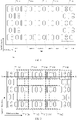
FIG. 1 is a schematic plan view of a display substrate according to an embodiment of the present disclosure; -
FIG. 2 is a schematic plan view of another display substrate according to an embodiment of the present disclosure; -
FIG. 3 is a schematic cross-sectional of a display substrate along an AA direction inFIG. 2 according to an embodiment of the present disclosure; -
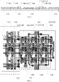
FIG. 4 is a partial plan view of another display substrate according to an embodiment of the present disclosure; -
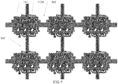
FIG. 5 is a partial plan view of a display substrate according to an embodiment of the present disclosure; -
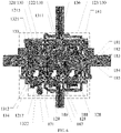
FIG. 6 is an enlarged schematic diagram of one first pixel group inFIG. 5 ; and -
FIG. 7 is a schematic diagram of a display device according to an embodiment of the present disclosure. - In order to make objects, technical solutions, and advantages of the embodiments of the present disclosure apparent, the technical solutions of the embodiments of the present disclosure will be described in a clearly and fully understandable way in connection with the drawings related to the embodiments of the present disclosure. Apparently, the described embodiments are just a part but not all of the embodiments of the present disclosure. Based on the described embodiments of the present disclosure, those skilled in the art can obtain other embodiment(s), without any inventive work, which should be within the scope of the present disclosure.
- Unless otherwise defined, all the technical and scientific terms used herein have the same meanings as commonly understood by one of ordinary skill in the art to which the present disclosure belongs. The terms "first," "second," etc., which are used in the present disclosure, are not intended to indicate any sequence, amount or importance, but distinguish various components. The terms "comprise," "comprising," "include," "including," etc., are intended to specify that the elements or the objects stated before these terms encompass the elements or the objects and equivalents thereof listed after these terms, but do not preclude the other elements or objects.
- With people's increasing requirements for the screen ratio of electronic products, the design of under-screen camera has become a research focus of major manufacturers. The main technical difficulty in the design of the under-screen camera is the low light transmittance of the screen, which seriously affects the imaging quality of the camera placed under the screen.
- With the improvement of consumers' requirements for screen integrity, the under-screen camera design is becoming more and more popular. At present, in the field of OLED, the main technical difficulty of the under-screen camera design is the low screen transmittance, which seriously affects the imaging quality of the camera placed under the screen. For example, the display screen can be divided into a first display region and a second display region, the camera can be arranged in the first display region, and the second display region can be a normal display region; by reducing the resolution of the first display region, the density of sub-pixels in the first display region can be reduced, thus increasing the light transmittance, and further realizing the under-screen camera function.
- The embodiments of the present disclosure also provides a display substrate and a display device. The display substrate includes a base substrate including a first display region and a second display region, the second display region at least partially surrounding the first display region; and a plurality of sub-pixels located on the base substrate and in the first display region and the second display region, a density of the sub-pixels in the first display region is less than a density of the sub-pixels in the second display region, each sub-pixel includes a pixel circuit, the plurality of sub-pixels include a first sub-pixel, a second sub-pixel and a third sub-pixel, the plurality of sub-pixels include a plurality of first pixel groups and a plurality of second pixel groups, the plurality of first pixel groups are located in the first display region, the plurality of second pixel groups are located in the second display region, the first display region includes a plurality of sub-display regions and a sub-light-transmitting region between the sub-display regions, the plurality of first pixel groups are arranged in one-to-one correspondence with the plurality of sub-display regions, each of the first pixel groups includes one of the first sub-pixels, one of the second sub-pixels and one of the third sub-pixels arranged in sequence in a first direction, each of the second pixel groups includes one of the first sub-pixels, one second sub-pixel pair and one of the third sub-pixels arranged in the first direction, the second sub-pixel pair includes two of the second sub-pixels arranged in a second direction. The display substrate adopts the pixel arrangement of real GRB in the first display region and the pixel arrangement of GGRB in the second display region; on the one hand, the display substrate can reduce the resolution or PPI (Pixel Per Inch) of the first display region, thereby increasing the light transmittance of the first display region; on the other hand, the second display region of the display substrate has higher resolution and display effect. In addition, because the first display region adopts the pixel arrangement of real GRB, the green sub-pixel has a larger luminous area, thus having a longer service life.
- Hereinafter, the display substrate and display device provided by the embodiment of the present disclosure will be described in detail with reference to the accompanying drawings.
-
FIG. 1 is a schematic plan view of a display substrate according to an embodiment of the present disclosure. As illustrated byFIG. 1 , thedisplay substrate 100 includes abase substrate 110 and a plurality of sub-pixels 120; thebase substrate 110 includes afirst display region 112 and asecond display region 114, and thesecond display region 114 at least partially surrounds thefirst display region 112;a plurality of sub-pixels 120 are located on thebase substrate 110, and located in thefirst display region 112 and thesecond display region 114, and a density of sub-pixels in thefirst display region 112 is less than a density of sub-pixels in thesecond display region 114; each sub-pixel 120 includes a pixel circuit. The plurality of sub-pixels 120 include first sub-pixels 121,second sub-pixels 122 and third sub-pixels 123. The plurality of sub-pixels 120 includes a plurality offirst pixel groups 141 and a plurality of second pixel groups 142. The plurality offirst pixel groups 141 are located in thefirst display region 112 and the plurality ofsecond pixel groups 142 are located in thesecond display region 114. Thefirst display region 112 includes a plurality ofsub-display regions 1124 and a sub-light-transmittingregion 1126 between thesub-display regions 1124. The plurality offirst pixel groups 141 are arranged in one-to-one correspondence with thesub-display regions 1124. Each of thefirst pixel groups 141 includes one first sub-pixel 121, onesecond sub-pixel 122 and one third sub-pixel 123 arranged in sequence along a first direction. Eachsecond pixel group 142 includes one first sub-pixel 121, onesecond sub-pixel pair 1220 and one third sub-pixel 123 arranged along the first direction, and thesecond sub-pixel pair 1220 includes twosecond sub-pixels 122 arranged along a second direction. - In the display substrate provided by the embodiment of the present disclosure, the
first display region 112 includes a plurality ofsub-display regions 1124 and a sub-light-transmittingregion 1126 between thesub-display regions 1124, and the plurality offirst pixel groups 141 are arranged in one-to-one correspondence with thesub-display regions 1124. At this time, the plurality of sub-display regions in thefirst display region 112 can be used for display, while the sub-light-transmittingregion 1126 can allow light to pass through, so thefirst display region 112 can be provided with photosensitive functional elements, such as a camera. Each of thefirst pixel groups 141 includes one first sub-pixel 121, onesecond sub-pixel 122, and one third sub-pixel 123 arranged in sequence along the first direction. It can be seen that the sub-pixels in thefirst display region 112 can adopt the pixel arrangement of real GRB. In this case, the light emitting area of the second sub-pixel is larger, thus having a longer service life. Eachsecond pixel group 142 includes one first sub-pixel 121, onesecond sub-pixel pair 1220 and one third sub-pixel 123 arranged along the first direction, and thesecond sub-pixel pair 1220 includes twosecond sub-pixels 122 arranged along the second direction. It can be seen that the sub-pixels in thesecond display region 114 can adopt the pixel arrangement of GGRB, thus having higher resolution and better display effect. It should be noted that, because the number of the sub-pixels in the first display region is small, in order to make the brightness of the whole display substrate uniform, the brightness of the sub-pixels in each first pixel group is greater than that of the sub-pixels in the second pixel group, the display substrate can have a longer service life by increasing the light emitting area of the second sub-pixels in the first pixel group. - For example, as illustrated by
FIG. 1 , an orthographic projection of thefirst display region 112 on thebase substrate 110 has a shape of rectangular, and thesecond display region 114 surrounds three edges of thefirst display region 112. Of course, embodiments of the present disclosure include but are not limited thereto. The orthographic projection of thefirst display region 112 on thebase substrate 110 can also have other shapes, such as circular or drop shape. In addition, thesecond display region 114 may also surround all edges of thefirst display region 112. - In some examples, the sub-light-transmitting
region 1126 is not provided with the sub-pixel 120. Therefore, the sub-light-transmittingregion 1126 can have higher light transmittance. - In some examples, the first direction is substantially perpendicular to the second direction. It should be noted that the above-mentioned situation that the first direction is substantially perpendicular to the second direction includes the case that the included angle between the first direction and the second direction is 90 degrees and the case that the included angle between the first direction and the second direction is 80-100 degrees.
- In some examples, the first sub-pixel 121 is configured to emit light of a first color, the
second sub-pixel 122 is configured to emit light of a second color, and the third sub-pixel 123 is configured to emit light of a third color. - For example, the first color is red, the second color is green and the third color is blue.
-
FIG. 2 is a schematic plan view of another display substrate according to an embodiment of the present disclosure;FIG. 3 is a schematic cross-sectional view of a display substrate along the AA direction inFIG. 2 according to an embodiment of the present disclosure. - As illustrated by
FIG. 2 andFIG. 3 , thedisplay substrate 100 further includes a plurality of first light-shieldinglayers 151 and a second light-shielding layer 152; the plurality of first light-shieldinglayers 151 and the plurality ofsub-display regions 1124 are arranged in one-to-one correspondence; each first light-shielding layer 151 is located at a side of the correspondingfirst pixel group 141 close to thebase substrate 110; the second light-shielding layer 152 is located in thesecond display region 114, and at a side of thesecond pixel groups 142 close to thebase substrate 110. Therefore, the first light-shielding layer 151 can prevent the light emitted by thefirst pixel group 141 from entering the photosensitive functional elements arranged in thefirst display region 112; similarly, the second light-shielding layer 152 can also prevent the light emitted by thesecond pixel group 142 from entering the photosensitive functional element arranged in thefirst display region 112, thus ensuring that the photosensitive functional element can realize its function with high quality. For example, the photosensitive functional element can be a camera. - For example, orthographic projections of the
pixel circuits 130 of the plurality of sub-pixels 120 in thefirst pixel group 141 on thebase substrate 110 fall within orthographic projections of the corresponding first light-shieldinglayers 151 on thebase substrate 110, so that the first light-shielding layer 151 can shield thepixel circuits 130 of the plurality of sub-pixels 120 in thefirst pixel group 141, and prevent light from entering the photosensitive functional element through slits between the signal lines of thepixel circuits 130. - For example, as illustrated by
FIG. 2 andFIG. 3 ,adjacent sub-display regions 1124 are arranged at an interval. Of course, embodiments of the present disclosure include, but are not limited to, two adjacent sub-display regions or more sub-display regions can be closely arranged to form a larger region. - In some examples, as illustrated by
FIG. 2 andFIG. 3 , the second light-shielding layer 151 can occupy the entire area of thesecond display region 114, while the first light-shieldinglayers 151 only occupy the area of thesub-display regions 1124 in thefirst display region 112, thus ensuring that thefirst display region 112 has certain light transmittance. - In some examples, as illustrated by
FIG. 2 , eachsub-display region 1124 includes threeunit regions 200 in which the first sub-pixel 121, thesecond sub-pixel 122 and the third sub-pixel 123 in thefirst pixel group 141 are respectively arranged. That is, oneunit region 200 is provided with one sub-pixel 120. Afirst spacing region 161 is arranged between thefirst pixel groups 141 adjacent in the first direction, thefirst spacing region 161 includes oneunit region 200, and asecond spacing region 162 is arranged between thefirst pixel groups 141 adjacent in the second direction, thesecond spacing region 162 includes threeunit regions 200 arranged in the first direction, and the sub-light-transmittingregion 1126 includes thefirst spacing region 161 and thesecond spacing region 162. In the display substrate provided by the example, the pixel per inch of the first display region is approximately 3/8 of the pixel per inch of the second display region, and the PPI of the first display region is approximately 1/2 of the PPI of the second display region. Therefore, the first display region has higher light transmittance, so that the photosensitive functional elements arranged in the first display region can have better performance. -
FIG. 4 is a partial plan view of another display substrate according to an embodiment of the present disclosure.FIG. 4 shows only power lines and pixel circuits of the first pixel group and the second pixel group. As illustrated byFIG. 4 , each sub-pixel 120 further includes apower line 128 extending along the second direction. Thepower line 128 is connected with thepixel circuit 130 and configured to apply a constant voltage to thepixel circuit 130. Thepower line 128 of at least one sub-pixel 120 in each of thefirst pixel groups 141 is electrically connected with the corresponding first light-shielding layer 151, and thepower line 128 of at least one sub-pixel 128 in eachsecond pixel group 142 is electrically connected with the second light-shielding layer 152. In the display substrate provided by this example, both the first light-shielding layer and the second light-shielding layer are connected to the power line, which can prevent the first light-shielding layer and the second light-shielding layer from floating during display, thus improving the display quality of the display substrate. - In some examples, as illustrated by
FIG. 4 , in order to reduce the area of each of thefirst pixel groups 141, thepower line 128 of the first sub-pixel 121 in each of thefirst pixel groups 141 is connected with the corresponding first light-shielding layer 151, while thepower line 128 of thesecond sub-pixel 122 and thepower line 128 of the third sub-pixel 123 in each of thefirst pixel groups 141 are not connected with the corresponding first light-shieldinglayers 151. Therefore, only thepower line 128 of the first sub-pixel 121 in each of thefirst pixel groups 141 applies a constant voltage to the first light-shielding layer 151 corresponding to thefirst pixel group 141. - In some examples, as illustrated by
FIG. 4 , thepower lines 128 of the first sub-pixel 121, thesecond sub-pixel 122 and the third sub-pixel 123 in eachsecond pixel group 142 are electrically connected with the corresponding second light-shielding layer 152. Of course, the embodiments of the present disclosure include but are not limited thereto, and only the power lines of some sub-pixels in each second pixel group can be connected with the corresponding second light-shielding layer. -
FIG. 5 is a partial plan view of a display substrate according to an embodiment of the present disclosure;FIG. 6 is an enlarged schematic diagram of one first pixel group inFIG. 5 . As illustrated byFIG. 5 andFIG. 6 , thepower line 128 of thesecond sub-pixel 122 in each of thefirst pixel groups 141 is connected to thepower line 128 of thesecond sub-pixel 122 in thefirst pixel group 141 adj acent to each other in the second direction through thesecond spacing region 162. Thepower lines 128 of the first sub-pixel 121 and the third sub-pixel 123 in each of thefirst pixel groups 141 are disconnected from thepower lines 128 of the first sub-pixel 121 and the third sub-pixel 123 in thefirst pixel group 141 adjacent to each other in the second direction. That is, thepower line 128 of the first sub-pixel 121 in each of thefirst pixel groups 141 is not connected with thepower line 128 of the first sub-pixel 121 in thefirst pixel group 141 adjacent in the second direction, and thepower line 128 of the third sub-pixel 123 in each of thefirst pixel groups 141 is not connected with thepower line 128 of the third sub-pixel 123 in thefirst pixel group 141 adjacent in the second direction. Therefore, the display substrate can reduce the number of traces in the second spacing region, thereby improving the light transmittance of the second spacing region. - It should be noted that, as illustrated by
FIG. 5 andFIG. 6 , thepower line 128 of the first sub-pixel 121, thepower line 128 of thesecond sub-pixel 122 and thepower line 128 of the third sub-pixel 123 in each of thefirst pixel groups 141 can be electrically connected with each other through a second gate layer in the pixel circuit. - In some examples, as illustrated by
FIG. 5 andFIG. 6 , thepixel circuit 130 of the sub-pixel 120 in each of thefirst pixel groups 141 includes a firstinitialization signal line 1311, a firstreset signal line 1321, a gate line 133, anemission control line 134, a secondinitialization signal line 1312 and a secondreset signal line 1322 extending in the first direction. In each of the first pixel groups 141, the first initialization signal line 1311 of the first sub-pixel 121, the first initialization signal line 1311 of the second sub-pixel 122 and the first initialization signal line 1311 of the third sub-pixel 123 are connected; in each of the first pixel groups 141, the first reset signal line 1321 of the first sub-pixel 121, the first reset signal line 1321 of the second sub-pixel 122 and the first reset signal line 1321 of the third sub-pixel 123 are connected; in each of the first pixel groups 141, the gate line 133 of the first sub-pixel 121, the gate line 133 of the second sub-pixel 122 and the gate line 133 of the third sub-pixel 123 are connected; in each of the first pixel groups 141, the emission control line 134 of the first sub-pixel 121, the emission control line 134 of the second sub-pixel 122 and the emission control line 134 of the third sub-pixel 123 are connected; in each of the first pixel groups 141, the second initialization signal line 1312 of the first sub-pixel 121, the second initialization signal line 1312 of the second sub-pixel 122 and the second initialization signal line 1312 of the third sub-pixel 123 are connected; in each of the first pixel groups 141, the second reset signal line 1322 of the first sub-pixel 121, the second reset signal line 1322 of the second sub-pixel 122 and the second reset signal line 1322 of the third sub-pixel 123 are connected. - It should be noted that in this disclosure, in order to more clearly explain the connection relationship of these signal lines, they are divided into signal line segments corresponding to respective sub-pixels. However, respective signal lines in each of the first pixel groups may be integrally formed. For example, as illustrated by
FIG. 5 , in each of thefirst pixel groups 141, the firstinitialization signal line 1311 of the first sub-pixel 121, the firstinitialization signal line 1311 of thesecond sub-pixel 122 and the firstinitialization signal line 1311 of the third sub-pixel 123 are integrally formed; the firstreset signal line 1321 of the first sub-pixel 121, the firstreset signal line 1321 of thesecond sub-pixel 122 and the firstreset signal line 1321 of the third sub-pixel 123 are integrally formed; the gate line 133 of the first sub-pixel 121, the gate line 133 of thesecond sub-pixel 122 and the gate line 133 of the third sub-pixel 123 are integrally formed; theemission control line 134 of the first sub-pixel 121, theemission control line 134 of thesecond sub-pixel 122 and theemission control line 134 of the third sub-pixel 123 are integrally formed; the secondinitialization signal line 1312 of the first sub-pixel 121, the secondinitialization signal line 1312 of thesecond sub-pixel 122 and the secondinitialization signal line 1312 of the third sub-pixel 123 are integrally formed; the secondreset signal line 1322 of the first sub-pixel 121, the secondreset signal line 1322 of thesecond sub-pixel 122 and the secondreset signal line 1322 of the third sub-pixel 123 are integrally formed. - In some examples, as illustrated by
FIG. 4 ,FIG. 5 andFIG. 6 , thepower lines 128 of the first sub-pixels 121 in each of thefirst pixel groups 141 are electrically connected with the corresponding first light-shieldinglayers 151 through the first light-shielding layer viaholes 171. For example, as illustrated byFIG. 4 ,FIG. 5 andFIG. 6 , onefirst pixel group 141 only includes one first light-shielding layer viahole 171. Thepower lines 128 of the first sub-pixel 121, thesecond sub-pixel 122 and the third sub-pixel 123 in eachsecond pixel group 142 are electrically connected with the second light-shielding layer 152 through the second light-shielding layer viaholes 172, respectively. An orthographic projection of the first light-shielding layer viahole 171 on thebase substrate 110 is located at a side of the secondreset signal line 1322 away from theemission control line 134. Therefore, the secondinitialization signal line 1312 and the secondreset signal line 1322 can be arranged closer to theemission control line 134, thereby reducing the area occupied by the pixel circuit, further reducing the area of the first light-shielding layer and improving the light transmittance of the first display region. In some examples, as illustrated byFIG. 5 andFIG. 6 , thepixel circuit 130 of the first sub-pixel 121 includes awiring region 1215 and a viahole region 1217; the firstinitialization signal line 1311, the firstreset signal line 1321, the gate line 133, theemission control line 134, the secondinitialization signal line 1312 and the secondreset signal line 1322 are disposed in thewiring region 1215; the viahole region 1217 is located on a side of thewiring region 1215 close to thesecond spacing region 162, and the first light-shielding layer via 171 is disposed in the viahole region 1217. Therefore, because of the first light-shielding layer viahole 171 is arranged in the viahole region 1217, the firstinitialization signal line 1311, the firstreset signal line 1321, the gate line 133, theemission control line 134, the secondinitialization signal line 1312 and the secondreset signal line 1322 can be more densely arranged in thewiring region 1215. Thus, the display substrate can reduce the area occupied by the pixel circuit, further reduce the area of the first light-shielding layer and improve the light transmittance of the first display region. - In some examples, as illustrated by
FIG. 5 andFIG. 6 , thepixel circuit 130 of the sub-pixel 120 in eachsecond pixel group 142 includes a firstinitialization signal line 1311, a firstreset signal line 1321, a gate line 133 and anemission control line 134 extending in the first direction. Extension lines of the secondinitialization signal line 1312 and the secondreset signal line 1322 of the first sub-pixel 121 in thefirst pixel group 141 are located between the firstemission control line 134 of the first sub-pixel 121 in thesecond pixel group 142 in the same row and the firstreset signal line 1311 of the first sub-pixel 121 in thesecond pixel group 142 in the next row. In the display substrate, the pixel circuits of the sub-pixels in each second pixel group do not need to provide second initialization signal lines and second reset signal lines, but the first initialization signal lines and first reset signal lines of the sub-pixels of the second pixel group in the next row are used as the second initialization signal lines and second reset signal lines of the sub-pixels of the second pixel group in the previous row; at this time, because of the extension lines of the second initialization signal line and the second reset signal line of the first sub-pixel in the first pixel group are located between the first emission control line of the first sub-pixel in the second pixel group in the same row and the first reset signal line of the first sub-pixel in the second pixel group in the next row, the display substrate can reduce the area occupied by pixel circuits of each sub-pixel in the first pixel group, thereby reducing the area of the first light-shielding layer and improving the light transmittance of the first display region. - In some examples, as illustrated by
FIG. 5 andFIG. 6 , the first initialization signal line 1311 of the third sub-pixel 123 in each of the first pixel groups 141 is connected with the first initialization signal line 1311 of the first sub-pixel 121 in the first pixel group 141 adjacent in the first direction through the first connecting line 181; the first reset signal line 1321 of the third sub-pixel 123 in each of the first pixel groups 141 is connected with the first reset signal line 1321 of the first sub-pixel 121 in the first pixel group 141 adjacent in the first direction through the second connecting line 182; the gate line 133 and the second reset signal line 1322 of the third sub-pixel 123 in each of the first pixel groups 141 are connected with the gate line 133 and the second reset signal line 1322 of the first sub-pixel 121 in the first pixel group 141 adjacent in the first direction through the third connecting line 183; the emission control line 124 of the third sub-pixel 123 in each of the first pixel groups 141 is connected with the emission control line 124 of the first sub-pixel 121 in the first pixel group 141 adjacent in the first direction through the fourth connecting line 184; the second initialization signal line 1312 of the third sub-pixel 123 in each of the first pixel groups 141 is connected with the second initialization signal line 1312 of the first sub-pixel 121 in the first pixel group 141 adjacent in the first direction through the fifth connecting line 185, and the first connecting line 181, the second connecting line 182, the third connecting line 183, the fourth connecting line 184 and the fifth connecting line 185 gather together in the first spacing region 161. For example, "gather together" in the present disclosure refers to that the arrangement density of the connecting lines is less than that of various signal lines connected with the connecting lines. For example, the first connecting line to fifth connecting line 181-185 are densely arranged in the second direction, while the various signal lines to which they are connected are more sparsely arranged in the second direction. Therefore, the first connecting line, the second connecting line, the third connecting line, the fourth connecting line and the fifth connecting line are gathered in the first spacing regions, so that the display substrate can reduce the area occupied by the first connecting line, the second connecting line, the third connecting line, the fourth connecting line and the fifth connecting line in the first spacing region, thereby improving the light transmittance of the first display region. - In some examples, as illustrated by
FIG. 5 andFIG. 6 , the first connectingline 181, the third connectingline 183 and the fifth connectingline 185 are arranged in the same layer as thepower line 128, and are arranged in different layers from the firstinitialization signal line 1311, the gate line 133 and the secondinitialization signal line 1312. For example, the first connectingline 181, the third connectingline 183 and the fifth connectingline 185 can be electrically connected with the firstinitialization signal line 1311, the gate line 133 and the secondinitialization signal line 1312 through via holes, respectively. - In some examples, as illustrated by
FIG. 5 andFIG. 6 , the second connectingline 182 and the firstreset signal line 1321 are arranged in the same layer and integrally formed, while the fourth connectingline 184 and theemission control line 134 are arranged in the same layer and integrally formed. Thus, the first connecting line, the third connecting line and the fifth connecting line are located in the same layer, and the second connecting line and the fourth connecting line are located in the same layer; the first connecting line, the third connecting line and the fifth connecting line are located in different film layers from the second connecting line and the fourth connecting line, so on the premise of ensuring mutual insulation, the first connecting line, the second connecting line, the third connecting line, the fourth connecting line and the fifth connecting line can be closely arranged, thereby further reducing the area occupied by the first connecting line, the second connecting line, the third connecting line, the fourth connecting line and the fifth connecting line. - In some examples, as illustrated by
FIG. 5 andFIG. 6 , the first connectingline 181, the second connectingline 182, the third connectingline 183, the fourth connectingline 184 and the fifth connectingline 185 are sequentially arranged in the second direction. Therefore, on the premise of mutual insulation, the first connecting line, the second connecting line, the third connecting line, the fourth connecting line and the fifth connecting line can be closely arranged, so that the areas occupied by the first connecting line, the second connecting line, the third connecting line, the fourth connecting line and the fifth connecting line can be further reduced. - In some examples, as illustrated by
FIG. 5 andFIG. 6 , thepixel circuit 130 further includes adata line 136 extending in the second direction; thedata line 136 of the first sub-pixel 121 in each of thefirst pixel groups 141 is connected with thedata line 136 of the first sub-pixel 121 in thefirst pixel group 141 adjacent in the second direction through the sixth connectingline 186, and thedata line 136 of thesecond sub-pixel 122 in each of thefirst pixel groups 141 is connected with thedata line 136 of thesecond sub-pixel 122 adjacent in the second direction through the seventh connectingline 187; thedata line 136 of the third sub-pixel 123 in each of thefirst pixel groups 141 is connected with thedata line 136 of the third sub-pixel 123 in thefirst pixel group 141 adjacent in the second direction through the eighth connectingline 188, and the sixth connectingline 186, the seventh connectingline 187 and the eighth connectingline 188 gather together in thesecond spacing region 162. Therefore, the display substrate can reduce the areas occupied by the sixth connecting line, the seventh connecting line and the eighth connecting line by gathering the sixth connecting line, the seventh connecting line and the eighth connecting line in the second spacing region, thereby improving the light transmittance of the first display region. - In some examples, as illustrated by
FIG. 5 andFIG. 6 , the sixth connectingline 186 and the firstinitialization signal line 1311 are arranged in the same layer and arranged in different layers from thedata line 136, the seventh connectingline 187 and thedata line 136 are arranged in the same layer and integrated formed, and the eighth connectingline 188 and the firstreset signal line 1321 are arranged in the same layer and arranged in different layers from thedata line 136. For example, the sixth connectingline 186 and the eighth connectingline 188 can be electrically connected with the correspondingdata lines 136 through via holes. Therefore, the sixth connecting line and the eighth connecting line are arranged in different layers from the data line, and the seventh connecting line and the data line are located in the same layer; That is to say, the film layers where the sixth connecting line and the eighth connecting line are located are different from the film layer where the seventh connecting line is located. Therefore, on the premise of ensuring mutual insulation, the sixth connecting line, the seventh connecting line and the eighth connecting line can be closely arranged, thereby further reducing the area occupied by the sixth connecting line, the seventh connecting line and the eighth connecting line. - In some examples, as illustrated by
FIG. 6 , the sixth connectingline 186, the eighth connectingline 188 and the seventh connectingline 187 are sequentially arranged in the first direction. - It should be noted that the number of the first pixel groups in the first display region in the display substrate provided by the embodiment of the present disclosure is not limited to the specific number of the first pixel groups in the first display region in the above drawings, but is set according to the specific size of the product.
- An embodiment of the present disclosure also provides a display device.
FIG. 7 is a schematic diagram of a display device according to an embodiment of the present disclosure. As illustrated byFIG. 7 , the display device 300 includes thedisplay substrate 100 described above. Therefore, the display device has technical effects corresponding to the beneficial technical effects of the display substrate, for details, please refer to the related description of the display substrate. - For example, the display device can be display devices such as Organic Light-Emitting Diode (OLED) displays, and any products or components with display functions such as televisions, digital cameras, mobile phones, watches, tablet computers, notebook computers, navigators, etc.
- In some examples, as illustrated by
FIG. 7 , the display device 300 further includes a photosensitivefunctional element 310, which is located at a side of the plurality of sub-pixels 120 close to thebase substrate 110, and an orthogonal projection of the photosensitivefunctional element 310 on thebase substrate 110 at least partially overlaps with thefirst display region 112. The photosensitivefunctional element 310 is configured to receive light from the side of the display substrate where the plurality of sub-pixels are located, thereby realizing various functions. - For example, the above-mentioned photosensitive
functional element 310 can be a camera, so that the display device can realize functions such as camera shooting while realizing a full-screen design. - The following points need to be explained:
- (1) In the drawings of the embodiments of the present disclosure, only the structures related to the embodiments of the present disclosure are involved, and other structures can refer to the general design.
- (2) The features of the same embodiment and different embodiments of the present disclosure can be combined with each other without conflict.
- The above are only the specific embodiments of this disclosure, but the scope of protection of the present disclosure is not limited thereto. Therefore, the scope of protection of the present disclosure should be based on the scope of protection of the claims.
Claims (24)
- A display substrate, comprising:a base substrate, comprising a first display region and a second display region, the second display region at least partially surrounding the first display region; anda plurality of sub-pixels, located on the base substrate and in the first display region and the second display region, a density of the sub-pixels in the first display region being less than a density of the sub-pixels in the second display region, each of the sub-pixels comprising a pixel circuit,wherein the plurality of sub-pixels comprise first sub-pixels, second sub-pixels and third sub-pixels, the plurality of sub-pixels comprise a plurality of first pixel groups and a plurality of second pixel groups, the plurality of first pixel groups are located in the first display region, the plurality of second pixel groups are located in the second display region,the first display region comprises a plurality of sub-display regions and a sub-light-transmitting region between the sub-display regions, the plurality of first pixel groups are arranged in one-to-one correspondence with the plurality of sub-display regions, each of the first pixel groups comprises one first sub-pixel of the first sub-pixels, one second sub-pixel of the second sub-pixels and one third sub-pixel of the third sub-pixels arranged in sequence in a first direction, each of the second pixel groups comprises one first sub-pixel of the first sub-pixels, one second sub-pixel pair and one third sub-pixel of the third sub-pixels arranged in the first direction, the second sub-pixel pair comprises two second sub-pixels of the second sub-pixels arranged in a second direction.
- The display substrate according to claim 1, further comprising:a plurality of first light-shielding layers, arranged in one-to-one correspondence with the plurality of sub-display regions, and each of the first light-shielding layers being located at a side of a corresponding one of the first pixel groups close to the base substrate; anda second light-shielding layer, located in the second display region and at a side of the plurality of second pixel groups close to the base substrate.
- The display substrate according to claim 2, wherein each of the sub-pixels further comprises a power line extending along the second direction, the power line being connected to the pixel circuit and configured to apply a constant voltage to the pixel circuit,
wherein the power line of at least one sub-pixel in each of the first pixel groups is electrically connected with a corresponding one of the first light-shielding layers, and the power line of at least one sub-pixel in each of the second pixel groups is electrically connected with the second light-shielding layer. - The display substrate according to claim 3, wherein the power line of the first sub-pixel in each of the first pixel groups is electrically connected with a corresponding one of the first light-shielding layers, and power lines of the first sub-pixel, the second sub-pixel and the third sub-pixel in each of the second pixel groups are electrically connected with the corresponding second light-shielding layer.
- The display substrate according to any one of claims 1-4, wherein each of the sub-display regions comprises three unit regions, and the first sub-pixel, the second sub-pixel and the third sub-pixel in one of the first pixel groups are respectively arranged in the three unit regions,a first spacing region is arranged between adjacent ones of the first pixel groups in the first direction, the first spacing region comprises one unit region, a second spacing region is arranged between adjacent ones of the first pixel groups in the second direction, and the second spacing region comprises three unit regions arranged in the first direction,the sub-light-transmitting region comprises the first spacing region and the second spacing region.
- The display substrate according to claim 5, wherein the power line of the second sub-pixel in each of the first pixel groups passes through the second spacing region and is connected to the power line of the second sub-pixel in an adjacent first pixel group in the second direction,
the power line of the first sub-pixel in each of the first pixel groups is disconnected from the power line of the first sub-pixel in an adjacent first pixel group in the second direction, the power line of the third sub-pixel in each of the first pixel groups is disconnected from the power line of the third sub-pixel in an adjacent first pixel group in the second direction. - The display substrate according to claim 5, wherein the pixel circuit of each of the sub-pixels in each of the first pixel groups comprises a first initialization signal line, a first reset signal line, a gate line, an emission control line, a second initialization signal line and a second reset signal line extending along the first direction,in each of the first pixel groups, the first initialization signal line of the first sub-pixel, the first initialization signal line of the second sub-pixel and the first initialization signal line of the third sub-pixel are connected,in each of the first pixel groups, the first reset signal line of the first sub-pixel, the first reset signal line of the second sub-pixel and the first reset signal line of the third sub-pixel are connected,in each of the first pixel groups, the gate line of the first sub-pixel, the gate line of the second sub-pixel and the gate line of the third sub-pixel are connected,in each of the first pixel groups, the emission control line of the first sub-pixel, the emission control line of the second sub-pixel and the emission control line of the third sub-pixel are connected,in each of the first pixel groups, the second initialization signal line of the first sub-pixel, the second initialization signal line of the second sub-pixel and the second initialization signal line of the third sub-pixel are connected,in each of the first pixel groups, the second reset signal line of the first sub-pixel, the second reset signal line of the second sub-pixel and the second reset signal line of the third sub-pixel are connected.
- The display substrate according to claim 7, wherein the power line of the first sub-pixel in each of the first pixel groups is electrically connected with a corresponding first light-shielding layer through a first light-shielding layer via hole,the power lines of the first sub-pixel, the second sub-pixel and the third sub-pixel in each of the second pixel groups are electrically connected with the second light-shielding layer through second light-shielding layer via holes,an orthographic projection of the first light-shielding layer via hole the on the base substrate is located at a side of the second reset signal line away from the emission control line.
- The display substrate according to claim 8, wherein one of the first pixel groups comprises only one first light-shielding layer via hole.
- The display substrate according to claim 8, wherein the pixel circuit of the first sub-pixel comprises:a wiring region, the first initialization signal line, the first reset signal line, the gate line, the emission control line, the second initialization signal line and the second reset signal line being arranged in the wiring region; anda via hole region, located at a side of the wiring region close to the second spacing region, wherein the first light-shielding layer via hole is arranged in the via hole region.
- The display substrate according to any one of claims 8-10, wherein the pixel circuit of each of the sub-pixels in each of the second pixel groups comprises a first initialization signal line, a first reset signal line, a gate line and an emission control line extending along the first direction,
the extension lines of the second initialization signal line and the second reset signal line of the first sub-pixel in one of the first pixel groups are located between the first emission control line of the first sub-pixel in one of the second pixel groups in the same row as the one of the first pixel groups and the first reset signal line of the first sub-pixel in one of the second pixel groups in a next row. - The display substrate according to any one of claims 7-11, wherein,the first initialization signal line of the third sub-pixel in each of the first pixel groups is connected with the first initialization signal line of the first sub-pixel in an adjacent one of the first pixel groups in the first direction through a first connecting line,the first reset signal line of the third sub-pixel in each of the first pixel groups is connected with the first reset signal line of the first sub-pixel in an adjacent one of the first pixel groups in the first direction through a second connecting line,the gate line and the second reset signal line of the third sub-pixel in each of the first pixel groups are connected by a third connecting line, and are connected with the gate line and the second reset signal line of the first sub-pixel in an adjacent one of first pixel groups in the first direction through the third connecting line,the emission control line of the third sub-pixel in each of the first pixel groups is connected with the emission control line of the first sub-pixel in an adjacent one of the first pixel groups in the first direction through a fourth connecting line,the second initialization signal line of the third sub-pixel in each of the first pixel groups is connected with the second initialization signal line of the first sub-pixel in an adjacent one of the first pixel groups in the first direction through a fifth connecting line,the first connecting line, the second connecting line, the third connecting line, the fourth connecting line and the fifth connecting line gather together in the first spacing region.
- The display substrate according to claim 12, wherein the first connecting line, the third connecting line and the fifth connecting line are arranged in the same layer as the power line, and are arranged in different layers from the first initialization signal line, the gate line and the second initialization signal line.
- The display substrate according to claim 13, wherein the second connecting line and the first reset signal line are arranged in the same layer and integrally formed, and the fourth connecting line and the emission control line are arranged in the same layer and integrally formed.
- The display substrate according to claim 13, wherein the first connecting line, the second connecting line, the third connecting line, the fourth connecting line and the fifth connecting line are sequentially arranged in the second direction.
- The display substrate according to claim 5, wherein the pixel circuit further comprises a data line extending along the second direction,the data line of the first sub-pixel in each of the first pixel groups is connected with the data line of the first sub-pixel in an adjacent one of the first pixel groups in the second direction through a sixth connecting line,the data line of the second sub-pixel in each of the first pixel groups is connected with the data line of the second sub-pixel in an adjacent one of the first pixel groups in the second direction through a seventh connecting line,the data line of the third sub-pixel in each of the first pixel groups is connected with the data line of the third sub-pixel in an adjacent one of the first pixel groups in the second direction through an eighth connecting line,the sixth connecting line, the seventh connecting line and the eighth connecting line gather together in the second spacing region.
- The display substrate according to claim 16, wherein the sixth connecting line and the first initialization signal line are arranged in the same layer, and are arranged in different layers from the data line, the seventh connecting line and the data line are arranged in the same layer and integrated formed, and the eighth connecting line and the first reset signal line are arranged in the same layer, and are arranged in different layers from the data line.
- The display substrate according to claim 17, wherein the sixth connecting line, the eighth connecting line and the seventh connecting line are sequentially arranged in the first direction.
- The display substrate according to any one of claims 1-18, wherein the sub-light-transmitting region is not provided with the sub-pixels.
- The display substrate according to any one of claims 1-18, wherein the first direction is substantially perpendicular to the second direction.
- The display substrate according to any one of claims 1-18, wherein the first sub-pixel is configured to emit light of a first color, the second sub-pixel is configured to emit light of a second color, and the third sub-pixel is configured to emit light of a third color.
- The display substrate according to claim 21, wherein the first color is red, the second color is green and the third color is blue.
- A display device, comprising the display substrate according to any one of claims 1-22.
- The display device according to claim 23, further comprising:a photosensitive functional element, located at a side of the plurality of sub-pixels close to the base substrate,wherein an orthographic projection of the photosensitive functional element on the base substrate at least partially overlaps with the first display region.
Priority Applications (1)
| Application Number | Priority Date | Filing Date | Title |
|---|---|---|---|
| EP25183417.2A EP4601444A3 (en) | 2020-06-30 | 2021-05-17 | Display substrate and display device |
Applications Claiming Priority (2)
| Application Number | Priority Date | Filing Date | Title |
|---|---|---|---|
| CN202010617909.7A CN113871417B (en) | 2020-06-30 | 2020-06-30 | Display substrate and display device |
| PCT/CN2021/094065 WO2022001421A1 (en) | 2020-06-30 | 2021-05-17 | Display substrate and display device |
Related Child Applications (2)
| Application Number | Title | Priority Date | Filing Date |
|---|---|---|---|
| EP25183417.2A Division EP4601444A3 (en) | 2020-06-30 | 2021-05-17 | Display substrate and display device |
| EP25183417.2A Division-Into EP4601444A3 (en) | 2020-06-30 | 2021-05-17 | Display substrate and display device |
Publications (3)
| Publication Number | Publication Date |
|---|---|
| EP4053907A1 true EP4053907A1 (en) | 2022-09-07 |
| EP4053907A4 EP4053907A4 (en) | 2023-06-21 |
| EP4053907B1 EP4053907B1 (en) | 2025-09-03 |
Family
ID=78981853
Family Applications (2)
| Application Number | Title | Priority Date | Filing Date |
|---|---|---|---|
| EP25183417.2A Pending EP4601444A3 (en) | 2020-06-30 | 2021-05-17 | Display substrate and display device |
| EP21832137.0A Active EP4053907B1 (en) | 2020-06-30 | 2021-05-17 | Display substrate and display device |
Family Applications Before (1)
| Application Number | Title | Priority Date | Filing Date |
|---|---|---|---|
| EP25183417.2A Pending EP4601444A3 (en) | 2020-06-30 | 2021-05-17 | Display substrate and display device |
Country Status (5)
| Country | Link |
|---|---|
| US (2) | US12581828B2 (en) |
| EP (2) | EP4601444A3 (en) |
| JP (2) | JP7853207B2 (en) |
| CN (3) | CN113871417B (en) |
| WO (1) | WO2022001421A1 (en) |
Families Citing this family (2)
| Publication number | Priority date | Publication date | Assignee | Title |
|---|---|---|---|---|
| CN115020461B (en) * | 2022-05-31 | 2025-09-16 | 京东方科技集团股份有限公司 | Display substrate and display device |
| CN116782703A (en) * | 2023-07-31 | 2023-09-19 | 上海天马微电子有限公司 | A display panel and display device |
Family Cites Families (34)
| Publication number | Priority date | Publication date | Assignee | Title |
|---|---|---|---|---|
| US9190456B2 (en) * | 2012-04-25 | 2015-11-17 | Ignis Innovation Inc. | High resolution display panel with emissive organic layers emitting light of different colors |
| JP6518890B2 (en) | 2014-03-31 | 2019-05-29 | 株式会社Joled | Display device and electronic device |
| TW201622112A (en) * | 2014-12-02 | 2016-06-16 | 群創光電股份有限公司 | Display panel |
| CN105629605B (en) | 2016-01-06 | 2019-01-22 | 深圳市华星光电技术有限公司 | Array substrate, liquid crystal display panel and liquid crystal display device |
| CN207264695U (en) * | 2017-09-30 | 2018-04-20 | 云谷(固安)科技有限公司 | Terminal and display screen |
| WO2019062221A1 (en) * | 2017-09-30 | 2019-04-04 | 云谷(固安)科技有限公司 | Display screen and display device |
| WO2019062236A1 (en) * | 2017-09-30 | 2019-04-04 | 昆山国显光电有限公司 | Display screen, display screen driving method and display device thereof |
| US10756156B2 (en) * | 2017-10-30 | 2020-08-25 | Samsung Display Co., Ltd. | Display device having enhanced UV light blocking and method for fabricating the same |
| KR102126552B1 (en) | 2017-12-19 | 2020-06-24 | 엘지디스플레이 주식회사 | Display device |
| CN110914891B (en) * | 2018-06-20 | 2021-11-26 | 京东方科技集团股份有限公司 | Display substrate, driving method thereof and display device |
| CN110827765B (en) | 2018-08-08 | 2021-04-09 | 京东方科技集团股份有限公司 | Display panel and driving method thereof, and display device |
| US10635374B2 (en) * | 2018-08-28 | 2020-04-28 | Innolux Corporation | Electronic device |
| KR102426708B1 (en) | 2018-09-07 | 2022-07-29 | 삼성디스플레이 주식회사 | Display apparatus |
| KR20200044245A (en) | 2018-10-18 | 2020-04-29 | 삼성디스플레이 주식회사 | Display device |
| CN109599419B (en) | 2018-10-23 | 2020-12-25 | 武汉华星光电半导体显示技术有限公司 | Array substrate and manufacturing method thereof |
| JP7149164B2 (en) * | 2018-11-02 | 2022-10-06 | 株式会社ジャパンディスプレイ | Display device |
| CN109541833A (en) | 2018-12-13 | 2019-03-29 | 华为技术有限公司 | Display component, display device and its driving method |
| CN109962092B (en) | 2019-03-29 | 2021-09-24 | 上海天马微电子有限公司 | A display panel and display device |
| CN110112189B (en) | 2019-04-25 | 2021-03-23 | 武汉华星光电半导体显示技术有限公司 | Display panel and display device |
| CN113284911B (en) * | 2019-04-30 | 2024-05-07 | 武汉天马微电子有限公司 | Display panel and display device |
| KR102698881B1 (en) * | 2019-05-23 | 2024-08-28 | 삼성디스플레이 주식회사 | Display device |
| CN111834375B (en) * | 2019-05-23 | 2022-11-08 | 昆山国显光电有限公司 | Display substrate, display panel and display device |
| CN110189627B (en) * | 2019-05-30 | 2021-12-24 | 武汉天马微电子有限公司 | Display panel and display device |
| CN110767720B (en) * | 2019-06-05 | 2020-09-08 | 昆山国显光电有限公司 | Display substrate, display panel and display device |
| CN110365819A (en) * | 2019-06-18 | 2019-10-22 | 武汉华星光电半导体显示技术有限公司 | Displays and Display Devices |
| CN110444125B (en) * | 2019-06-25 | 2022-03-08 | 荣耀终端有限公司 | Display screen and terminal |
| CN110416278B (en) | 2019-08-06 | 2022-09-27 | 京东方科技集团股份有限公司 | Display substrate, preparation method thereof and display device |
| CN110534541A (en) | 2019-08-30 | 2019-12-03 | 武汉天马微电子有限公司 | Electroluminescent display panel and display device |
| CN110649085A (en) * | 2019-10-23 | 2020-01-03 | 信利(惠州)智能显示有限公司 | Display panel and display device |
| CN110729337A (en) | 2019-11-15 | 2020-01-24 | 京东方科技集团股份有限公司 | Display substrate, manufacturing method thereof and electronic device |
| CN110767739B (en) | 2019-11-28 | 2025-09-09 | 京东方科技集团股份有限公司 | Display substrate and display device |
| CN111063719B (en) * | 2019-12-30 | 2022-08-12 | 武汉天马微电子有限公司 | Display panel and display device |
| CN114999361B (en) | 2020-01-03 | 2024-12-06 | 武汉天马微电子有限公司 | Display panel and display device |
| CN111192978B (en) | 2020-02-26 | 2022-08-09 | 武汉天马微电子有限公司 | Display panel and display device |
-
2020
- 2020-06-30 CN CN202010617909.7A patent/CN113871417B/en active Active
- 2020-06-30 CN CN202210226103.4A patent/CN114597247B/en active Active
- 2020-06-30 CN CN202410493502.6A patent/CN118368934A/en active Pending
-
2021
- 2021-05-17 EP EP25183417.2A patent/EP4601444A3/en active Pending
- 2021-05-17 WO PCT/CN2021/094065 patent/WO2022001421A1/en not_active Ceased
- 2021-05-17 JP JP2022533595A patent/JP7853207B2/en active Active
- 2021-05-17 EP EP21832137.0A patent/EP4053907B1/en active Active
- 2021-05-17 US US17/782,333 patent/US12581828B2/en active Active
-
2022
- 2022-11-09 US US17/984,055 patent/US12660460B2/en active Active
-
2026
- 2026-04-16 JP JP2026067633A patent/JP2026120729A/en active Pending
Also Published As
| Publication number | Publication date |
|---|---|
| CN113871417B (en) | 2025-07-04 |
| US12660460B2 (en) | 2026-06-16 |
| EP4601444A2 (en) | 2025-08-13 |
| CN114597247B (en) | 2025-03-07 |
| JP2023531341A (en) | 2023-07-24 |
| JP2026120729A (en) | 2026-07-22 |
| EP4053907A4 (en) | 2023-06-21 |
| EP4053907B1 (en) | 2025-09-03 |
| CN114597247A (en) | 2022-06-07 |
| CN118368934A (en) | 2024-07-19 |
| CN113871417A (en) | 2021-12-31 |
| US20230067919A1 (en) | 2023-03-02 |
| US20230039046A1 (en) | 2023-02-09 |
| US12581828B2 (en) | 2026-03-17 |
| WO2022001421A1 (en) | 2022-01-06 |
| KR20230028200A (en) | 2023-02-28 |
| EP4601444A3 (en) | 2025-11-05 |
| JP7853207B2 (en) | 2026-04-28 |
Similar Documents
| Publication | Publication Date | Title |
|---|---|---|
| US12190801B2 (en) | Display panel and display device | |
| CN111223908B (en) | Under-screen camera display module and electroluminescent display screen | |
| US12284871B2 (en) | Display substrate, display panel and display device | |
| KR20210138780A (en) | Display panel and display device | |
| CN110676296B (en) | Display panel and display device | |
| KR102918461B1 (en) | Display panels and display devices | |
| WO2023000832A1 (en) | Display module and display apparatus | |
| CN110275358A (en) | Display panel and display device | |
| US12389772B2 (en) | Display panel and electronic device | |
| CN113238402B (en) | Display panel and display device | |
| US20240315118A1 (en) | Display panel | |
| KR20150140498A (en) | Organic light emitting display device | |
| CN113299720B (en) | Display panel and display device | |
| US20240021146A1 (en) | Display substrate, display panel, and display device | |
| CN110875361A (en) | Display substrate and display device | |
| US12400580B2 (en) | Display panel and display apparatus | |
| US20230067919A1 (en) | Display substrate and display device | |
| US20250040380A1 (en) | Display module and display device | |
| EP4333022A1 (en) | Display panel and display apparatus | |
| CN110459563A (en) | Display panels and electronic equipment | |
| CN117596954A (en) | A display substrate and display device | |
| EP4421846A1 (en) | Display substrate and display device | |
| CN116471880B (en) | Display panel, display panel design method and display device | |
| EP4593567A1 (en) | Display substrate and display apparatus | |
| CN117957941A (en) | Display panel and display device |
Legal Events
| Date | Code | Title | Description |
|---|---|---|---|
| STAA | Information on the status of an ep patent application or granted ep patent |
Free format text: STATUS: THE INTERNATIONAL PUBLICATION HAS BEEN MADE |
|
| PUAI | Public reference made under article 153(3) epc to a published international application that has entered the european phase |
Free format text: ORIGINAL CODE: 0009012 |
|
| STAA | Information on the status of an ep patent application or granted ep patent |
Free format text: STATUS: REQUEST FOR EXAMINATION WAS MADE |
|
| 17P | Request for examination filed |
Effective date: 20220530 |
|
| AK | Designated contracting states |
Kind code of ref document: A1 Designated state(s): AL AT BE BG CH CY CZ DE DK EE ES FI FR GB GR HR HU IE IS IT LI LT LU LV MC MK MT NL NO PL PT RO RS SE SI SK SM TR |
|
| REG | Reference to a national code |
Ref legal event code: R079 Ref country code: DE Ref legal event code: R079 Ref document number: 602021037936 Country of ref document: DE Free format text: PREVIOUS MAIN CLASS: H01L0027320000 Ipc: H10K0059126000 |
|
| A4 | Supplementary search report drawn up and despatched |
Effective date: 20230524 |
|
| RIC1 | Information provided on ipc code assigned before grant |
Ipc: H10K 59/65 20230101ALI20230517BHEP Ipc: H10K 59/131 20230101ALI20230517BHEP Ipc: H10K 59/126 20230101AFI20230517BHEP |
|
| DAV | Request for validation of the european patent (deleted) | ||
| DAX | Request for extension of the european patent (deleted) | ||
| REG | Reference to a national code |
Ref country code: DE Ref legal event code: R079 Free format text: PREVIOUS MAIN CLASS: H10K0059126000 Ipc: H10K0059350000 Ref document number: 602021037936 Country of ref document: DE |
|
| RIC1 | Information provided on ipc code assigned before grant |
Ipc: H10K 59/80 20230101ALI20250226BHEP Ipc: H10K 59/65 20230101ALI20250226BHEP Ipc: H10K 59/131 20230101ALI20250226BHEP Ipc: H10K 59/126 20230101ALI20250226BHEP Ipc: H10K 59/35 20230101AFI20250226BHEP |
|
| GRAP | Despatch of communication of intention to grant a patent |
Free format text: ORIGINAL CODE: EPIDOSNIGR1 |
|
| STAA | Information on the status of an ep patent application or granted ep patent |
Free format text: STATUS: GRANT OF PATENT IS INTENDED |
|
| INTG | Intention to grant announced |
Effective date: 20250408 |
|
| GRAS | Grant fee paid |
Free format text: ORIGINAL CODE: EPIDOSNIGR3 |
|
| GRAA | (expected) grant |
Free format text: ORIGINAL CODE: 0009210 |
|
| STAA | Information on the status of an ep patent application or granted ep patent |
Free format text: STATUS: THE PATENT HAS BEEN GRANTED |
|
| AK | Designated contracting states |
Kind code of ref document: B1 Designated state(s): AL AT BE BG CH CY CZ DE DK EE ES FI FR GB GR HR HU IE IS IT LI LT LU LV MC MK MT NL NO PL PT RO RS SE SI SK SM TR |
|
| REG | Reference to a national code |
Ref country code: CH Ref legal event code: EP |
|
| REG | Reference to a national code |
Ref country code: DE Ref legal event code: R096 Ref document number: 602021037936 Country of ref document: DE |
|
| REG | Reference to a national code |
Ref country code: IE Ref legal event code: FG4D |
|
| REG | Reference to a national code |
Ref country code: NL Ref legal event code: MP Effective date: 20250903 |
|
| PG25 | Lapsed in a contracting state [announced via postgrant information from national office to epo] |
Ref country code: NO Free format text: LAPSE BECAUSE OF FAILURE TO SUBMIT A TRANSLATION OF THE DESCRIPTION OR TO PAY THE FEE WITHIN THE PRESCRIBED TIME-LIMIT Effective date: 20251203 |
|
| REG | Reference to a national code |
Ref country code: LT Ref legal event code: MG9D |
|
| PG25 | Lapsed in a contracting state [announced via postgrant information from national office to epo] |
Ref country code: FI Free format text: LAPSE BECAUSE OF FAILURE TO SUBMIT A TRANSLATION OF THE DESCRIPTION OR TO PAY THE FEE WITHIN THE PRESCRIBED TIME-LIMIT Effective date: 20250903 |
|
| PG25 | Lapsed in a contracting state [announced via postgrant information from national office to epo] |
Ref country code: HR Free format text: LAPSE BECAUSE OF FAILURE TO SUBMIT A TRANSLATION OF THE DESCRIPTION OR TO PAY THE FEE WITHIN THE PRESCRIBED TIME-LIMIT Effective date: 20250903 |
|
| PG25 | Lapsed in a contracting state [announced via postgrant information from national office to epo] |
Ref country code: GR Free format text: LAPSE BECAUSE OF FAILURE TO SUBMIT A TRANSLATION OF THE DESCRIPTION OR TO PAY THE FEE WITHIN THE PRESCRIBED TIME-LIMIT Effective date: 20251204 |
|
| PG25 | Lapsed in a contracting state [announced via postgrant information from national office to epo] |
Ref country code: SE Free format text: LAPSE BECAUSE OF FAILURE TO SUBMIT A TRANSLATION OF THE DESCRIPTION OR TO PAY THE FEE WITHIN THE PRESCRIBED TIME-LIMIT Effective date: 20250903 |
|
| PG25 | Lapsed in a contracting state [announced via postgrant information from national office to epo] |
Ref country code: LV Free format text: LAPSE BECAUSE OF FAILURE TO SUBMIT A TRANSLATION OF THE DESCRIPTION OR TO PAY THE FEE WITHIN THE PRESCRIBED TIME-LIMIT Effective date: 20250903 |
|
| PG25 | Lapsed in a contracting state [announced via postgrant information from national office to epo] |
Ref country code: BG Free format text: LAPSE BECAUSE OF FAILURE TO SUBMIT A TRANSLATION OF THE DESCRIPTION OR TO PAY THE FEE WITHIN THE PRESCRIBED TIME-LIMIT Effective date: 20250903 Ref country code: PL Free format text: LAPSE BECAUSE OF FAILURE TO SUBMIT A TRANSLATION OF THE DESCRIPTION OR TO PAY THE FEE WITHIN THE PRESCRIBED TIME-LIMIT Effective date: 20250903 |
|
| PG25 | Lapsed in a contracting state [announced via postgrant information from national office to epo] |
Ref country code: RS Free format text: LAPSE BECAUSE OF FAILURE TO SUBMIT A TRANSLATION OF THE DESCRIPTION OR TO PAY THE FEE WITHIN THE PRESCRIBED TIME-LIMIT Effective date: 20251203 |
|
| PG25 | Lapsed in a contracting state [announced via postgrant information from national office to epo] |
Ref country code: ES Free format text: LAPSE BECAUSE OF FAILURE TO SUBMIT A TRANSLATION OF THE DESCRIPTION OR TO PAY THE FEE WITHIN THE PRESCRIBED TIME-LIMIT Effective date: 20250903 |
|
| REG | Reference to a national code |
Ref country code: AT Ref legal event code: MK05 Ref document number: 1834809 Country of ref document: AT Kind code of ref document: T Effective date: 20250903 |
|
| PG25 | Lapsed in a contracting state [announced via postgrant information from national office to epo] |
Ref country code: NL Free format text: LAPSE BECAUSE OF FAILURE TO SUBMIT A TRANSLATION OF THE DESCRIPTION OR TO PAY THE FEE WITHIN THE PRESCRIBED TIME-LIMIT Effective date: 20250903 |
|
| PG25 | Lapsed in a contracting state [announced via postgrant information from national office to epo] |
Ref country code: SM Free format text: LAPSE BECAUSE OF FAILURE TO SUBMIT A TRANSLATION OF THE DESCRIPTION OR TO PAY THE FEE WITHIN THE PRESCRIBED TIME-LIMIT Effective date: 20250903 |
|
| PGFP | Annual fee paid to national office [announced via postgrant information from national office to epo] |
Ref country code: GB Payment date: 20260323 Year of fee payment: 6 |
|
| PG25 | Lapsed in a contracting state [announced via postgrant information from national office to epo] |
Ref country code: AT Free format text: LAPSE BECAUSE OF FAILURE TO SUBMIT A TRANSLATION OF THE DESCRIPTION OR TO PAY THE FEE WITHIN THE PRESCRIBED TIME-LIMIT Effective date: 20250903 |
|
| PG25 | Lapsed in a contracting state [announced via postgrant information from national office to epo] |
Ref country code: IT Free format text: LAPSE BECAUSE OF FAILURE TO SUBMIT A TRANSLATION OF THE DESCRIPTION OR TO PAY THE FEE WITHIN THE PRESCRIBED TIME-LIMIT Effective date: 20250903 |
|
| PG25 | Lapsed in a contracting state [announced via postgrant information from national office to epo] |
Ref country code: IS Free format text: LAPSE BECAUSE OF FAILURE TO SUBMIT A TRANSLATION OF THE DESCRIPTION OR TO PAY THE FEE WITHIN THE PRESCRIBED TIME-LIMIT Effective date: 20260103 |
|
| PG25 | Lapsed in a contracting state [announced via postgrant information from national office to epo] |
Ref country code: PT Free format text: LAPSE BECAUSE OF FAILURE TO SUBMIT A TRANSLATION OF THE DESCRIPTION OR TO PAY THE FEE WITHIN THE PRESCRIBED TIME-LIMIT Effective date: 20260105 Ref country code: CZ Free format text: LAPSE BECAUSE OF FAILURE TO SUBMIT A TRANSLATION OF THE DESCRIPTION OR TO PAY THE FEE WITHIN THE PRESCRIBED TIME-LIMIT Effective date: 20250903 |
|
| PG25 | Lapsed in a contracting state [announced via postgrant information from national office to epo] |
Ref country code: SK Free format text: LAPSE BECAUSE OF FAILURE TO SUBMIT A TRANSLATION OF THE DESCRIPTION OR TO PAY THE FEE WITHIN THE PRESCRIBED TIME-LIMIT Effective date: 20250903 Ref country code: EE Free format text: LAPSE BECAUSE OF FAILURE TO SUBMIT A TRANSLATION OF THE DESCRIPTION OR TO PAY THE FEE WITHIN THE PRESCRIBED TIME-LIMIT Effective date: 20250903 |
|
| REG | Reference to a national code |
Ref country code: DE Ref legal event code: R097 Ref document number: 602021037936 Country of ref document: DE |
|
| PG25 | Lapsed in a contracting state [announced via postgrant information from national office to epo] |
Ref country code: LT Free format text: LAPSE BECAUSE OF FAILURE TO SUBMIT A TRANSLATION OF THE DESCRIPTION OR TO PAY THE FEE WITHIN THE PRESCRIBED TIME-LIMIT Effective date: 20250903 |
|
| PG25 | Lapsed in a contracting state [announced via postgrant information from national office to epo] |
Ref country code: DK Free format text: LAPSE BECAUSE OF FAILURE TO SUBMIT A TRANSLATION OF THE DESCRIPTION OR TO PAY THE FEE WITHIN THE PRESCRIBED TIME-LIMIT Effective date: 20250903 |
|
| PLBE | No opposition filed within time limit |
Free format text: ORIGINAL CODE: 0009261 |
|
| STAA | Information on the status of an ep patent application or granted ep patent |
Free format text: STATUS: NO OPPOSITION FILED WITHIN TIME LIMIT |
|
| PGFP | Annual fee paid to national office [announced via postgrant information from national office to epo] |
Ref country code: DE Payment date: 20260520 Year of fee payment: 6 |
|
| REG | Reference to a national code |
Ref country code: CH Ref legal event code: L10 Free format text: ST27 STATUS EVENT CODE: U-0-0-L10-L00 (AS PROVIDED BY THE NATIONAL OFFICE) Effective date: 20260715 |
|
| PGFP | Annual fee paid to national office [announced via postgrant information from national office to epo] |
Ref country code: FR Payment date: 20260519 Year of fee payment: 6 |
|
| 26N | No opposition filed |
Effective date: 20260604 |