EP4053729B1 - Verfahren und vorrichtung zum vergleichen von chipprodukten, verfahren und vorrichtung zum modellieren von chipprodukten und speichermedium - Google Patents
Verfahren und vorrichtung zum vergleichen von chipprodukten, verfahren und vorrichtung zum modellieren von chipprodukten und speichermedium Download PDFInfo
- Publication number
- EP4053729B1 EP4053729B1 EP21844610.2A EP21844610A EP4053729B1 EP 4053729 B1 EP4053729 B1 EP 4053729B1 EP 21844610 A EP21844610 A EP 21844610A EP 4053729 B1 EP4053729 B1 EP 4053729B1
- Authority
- EP
- European Patent Office
- Prior art keywords
- chip product
- dimensional
- slice
- feature
- chip
- Prior art date
- Legal status (The legal status is an assumption and is not a legal conclusion. Google has not performed a legal analysis and makes no representation as to the accuracy of the status listed.)
- Active
Links
Images
Classifications
-
- G—PHYSICS
- G06—COMPUTING OR CALCULATING; COUNTING
- G06T—IMAGE DATA PROCESSING OR GENERATION, IN GENERAL
- G06T7/00—Image analysis
- G06T7/0002—Inspection of images, e.g. flaw detection
- G06T7/0004—Industrial image inspection
- G06T7/001—Industrial image inspection using an image reference approach
-
- G—PHYSICS
- G06—COMPUTING OR CALCULATING; COUNTING
- G06N—COMPUTING ARRANGEMENTS BASED ON SPECIFIC COMPUTATIONAL MODELS
- G06N3/00—Computing arrangements based on biological models
- G06N3/02—Neural networks
-
- G—PHYSICS
- G06—COMPUTING OR CALCULATING; COUNTING
- G06T—IMAGE DATA PROCESSING OR GENERATION, IN GENERAL
- G06T17/00—Three-dimensional [3D] modelling for computer graphics
-
- G—PHYSICS
- G06—COMPUTING OR CALCULATING; COUNTING
- G06T—IMAGE DATA PROCESSING OR GENERATION, IN GENERAL
- G06T19/00—Manipulating three-dimensional [3D] models or images for computer graphics
- G06T19/003—Navigation within 3D models or images
-
- G—PHYSICS
- G06—COMPUTING OR CALCULATING; COUNTING
- G06V—IMAGE OR VIDEO RECOGNITION OR UNDERSTANDING
- G06V10/00—Arrangements for image or video recognition or understanding
- G06V10/70—Arrangements for image or video recognition or understanding using pattern recognition or machine learning
- G06V10/74—Image or video pattern matching; Proximity measures in feature spaces
- G06V10/75—Organisation of the matching processes, e.g. simultaneous or sequential comparisons of image or video features; Coarse-fine approaches, e.g. multi-scale approaches; using context analysis; Selection of dictionaries
- G06V10/754—Organisation of the matching processes, e.g. simultaneous or sequential comparisons of image or video features; Coarse-fine approaches, e.g. multi-scale approaches; using context analysis; Selection of dictionaries involving a deformation of the sample pattern or of the reference pattern; Elastic matching
-
- G—PHYSICS
- G06—COMPUTING OR CALCULATING; COUNTING
- G06V—IMAGE OR VIDEO RECOGNITION OR UNDERSTANDING
- G06V10/00—Arrangements for image or video recognition or understanding
- G06V10/70—Arrangements for image or video recognition or understanding using pattern recognition or machine learning
- G06V10/82—Arrangements for image or video recognition or understanding using pattern recognition or machine learning using neural networks
-
- G—PHYSICS
- G06—COMPUTING OR CALCULATING; COUNTING
- G06V—IMAGE OR VIDEO RECOGNITION OR UNDERSTANDING
- G06V20/00—Scenes; Scene-specific elements
- G06V20/60—Type of objects
- G06V20/64—Three-dimensional [3D] objects
- G06V20/647—Three-dimensional [3D] objects by matching two-dimensional images to three-dimensional objects
-
- G—PHYSICS
- G06—COMPUTING OR CALCULATING; COUNTING
- G06F—ELECTRIC DIGITAL DATA PROCESSING
- G06F30/00—Computer-aided design [CAD]
- G06F30/20—Design optimisation, verification or simulation
- G06F30/27—Design optimisation, verification or simulation using machine learning, e.g. artificial intelligence, neural networks, support vector machines [SVM] or training a model
-
- G—PHYSICS
- G06—COMPUTING OR CALCULATING; COUNTING
- G06F—ELECTRIC DIGITAL DATA PROCESSING
- G06F30/00—Computer-aided design [CAD]
- G06F30/30—Circuit design
- G06F30/39—Circuit design at the physical level
- G06F30/398—Design verification or optimisation, e.g. using design rule check [DRC], layout versus schematics [LVS] or finite element methods [FEM]
-
- G—PHYSICS
- G06—COMPUTING OR CALCULATING; COUNTING
- G06T—IMAGE DATA PROCESSING OR GENERATION, IN GENERAL
- G06T2207/00—Indexing scheme for image analysis or image enhancement
- G06T2207/10—Image acquisition modality
- G06T2207/10016—Video; Image sequence
- G06T2207/10021—Stereoscopic video; Stereoscopic image sequence
-
- G—PHYSICS
- G06—COMPUTING OR CALCULATING; COUNTING
- G06T—IMAGE DATA PROCESSING OR GENERATION, IN GENERAL
- G06T2207/00—Indexing scheme for image analysis or image enhancement
- G06T2207/20—Special algorithmic details
- G06T2207/20084—Artificial neural networks [ANN]
-
- G—PHYSICS
- G06—COMPUTING OR CALCULATING; COUNTING
- G06T—IMAGE DATA PROCESSING OR GENERATION, IN GENERAL
- G06T2207/00—Indexing scheme for image analysis or image enhancement
- G06T2207/30—Subject of image; Context of image processing
- G06T2207/30108—Industrial image inspection
- G06T2207/30148—Semiconductor; IC; Wafer
-
- G—PHYSICS
- G06—COMPUTING OR CALCULATING; COUNTING
- G06T—IMAGE DATA PROCESSING OR GENERATION, IN GENERAL
- G06T2219/00—Indexing scheme for manipulating 3D models or images for computer graphics
- G06T2219/012—Dimensioning, tolerancing
Definitions
- the present disclosure relates to the field of semiconductors, and particularly to a comparison method for a chip product, an electronic device and a computer-readable storage medium.
- Chip is a general name for a semiconductor element product.
- the chip or called an Integrated Circuit (IC)
- IC Integrated Circuit
- a microcircuit or a microchip is a miniaturized circuit (mainly including a semiconductor device, as well as a passive component, etc.) in electronics and generally manufactured on a semiconductor wafer surface.
- a method for comparing and analyzing a chip product includes the following operations. After the chip product is analyzed, a series of discontinuous two-dimensional pictures are acquired, and specific information of a related parameter is manually marked on the picture by a professional. The parameter of chip product and the pictures are manually sorted and stored via an electronic file. When comparison and analysis is performed, the electronic file of the chip product to be compared and checked needs to be selected, and various parameter values are searched from the electronic files for manual comparison.
- Chip that is, an integrated circuit
- Chip is a strategic, fundamental and leading industry for national economic and social development and plays a key role in several major fields such as a computer, consumer electronics, network communication, and automotive electronics.
- the comparison of the chip product is mainly performed manually.
- the chip product is analyzed to obtain a two-dimensional picture of a cross section of the chip product.
- a related parameter is manually marked in the two-dimensional picture, then, the marked two-dimensional picture is sorted into an electronic file, and different files are configured to store the parameters and the pictures of different chip products.
- multiple files need to be opened manually, each parameter is searched for manual comparison, so that the comparison efficiency is low, and the solution of manual correspondence and marking is relatively poor in accuracy.
- the present disclosure provides a modeling method and comparison method for a chip product.
- the overall idea of the solution is that in a process of solving the above problems, the inventor found that with respect to the same chip product, an internal structure thereof is the same, parameter information of different positions or chips is also consistent, therefore, if the chip product can be digitally modeled, the above problems may be solved through a system automatic comparison model.
- a cross section image of the chip product is continuously acquired, the acquired images are analyzed, and a three-dimensional stereoscopic model is constructed based on an analysis result.
- the internal structure of the chip product and related parameter information may be visually checked, and the problem that a specific position cannot be positioned when the chip product is compared is solved.
- the same parameter information or different parameter information, etc. between the chip products may be automatically detected, structures of different positions and pictures of corresponding interfaces may also be directly checked, so that the problems that the comparison of the chip products are poor in efficiency and accuracy are effectively solved.
- the solution is applied to a computer device with computing capability, such as a computer, a personal computer, a smartphone, and other electronic device.
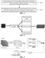
- FIG. 1 is a flowchart of a modeling method for a chip product according to a first embodiment of the present disclosure. As shown in FIG. 1 , the modeling method for the chip product specifically includes the operations S101 to S102.
- a slice sequence of a to-be-modeled chip product is acquired.
- the slice sequence includes multiple continuous slice images acquired by slicing the chip product.
- the slice sequence of the chip product needs to be acquired first.
- the slice sequence is actually a sequence of some continuous images. These images are the slice images of the chip product.
- the chip product may be continuously sliced according to a certain structure or slicing interval and an image of each slicing section is obtained through shooting or scanning, then multiple continuous slice images are obtained, that is, the slice sequence is obtained.
- the three-dimensional stereoscopic model is used for comparison of parameter information and the slice image between chip products when the chip products are compared.
- the slice sequence is recombined and constructed through the neural network to obtain the three-dimensional stereoscopic model of the chip product.
- a specific modeling process is implemented in the following implementations.
- the neural network involved in the solution includes a residual network, a U-net network model, and a multi-granularity network model.
- each slice image in the slice sequence is input into the residual network for feature extraction to acquire a first image feature of each slice image.
- the slice sequence is segmented through the U-net network model.
- Each slice image in the segmented slice sequence is input into the residual network for feature extraction to obtain a second image feature of each slice image.
- the first image feature is a feature directly extracted from the slice image by adopting the residual network
- the second image feature is the feature extracted by segmenting the slice image into small blocks first and then inputting the small blocks into the residual network.
- the first image feature and the second image feature of each slice image are merged to acquire an image feature of the slice image.
- the image feature of the slice image indicates the feature of the image itself. By merging the first image feature and the second image feature, the accuracy of the acquired slice image can be effectively improved.
- the image feature includes a color feature, a texture feature, a shape feature, a depth feature, etc.
- the image feature of each slice image in the slice sequence includes: a structural feature in the slice image and information about correlation between the slice image and preceding and following images of the slice image in the slice sequence.
- the three-dimensional stereoscopic model corresponding to the chip product is constructed by adopting the multi-granularity network model according to the slice sequence and the image feature of each slice image.
- a grid-shaped three-dimensional geometric shape may be generated according to multiple slice images in the slice sequence by adopting the multi-granularity network model and by taking a center of the chip product as the center of a three-dimensional coordinate system. Then image feature of each slice image is embedded into the three-dimensional geometric shape and the training is performed to obtain the three-dimensional stereoscopic model.
- the chip product is modeled by using a neural network based on the slice sequence of the chip product in advance to obtain the three-dimensional stereoscopic model.
- the chip products are compared, there is no need to manually compare pictures through multiple electronic files and no need to process a large amount of information, so that the comparison efficiency and accuracy of the chip products are improved.
- FIG. 2 is a schematic diagram of constructing three-dimensional stereoscopic model of a chip product according to an embodiment of the present disclosure. As shown in FIG. 2 , based on the above embodiments, multiple sub-networks are constructed for extracting information about correlation between upper and lower images, and an overall neural network model is constructed by the multiple sub-networks. After the chip product (that is, a chip in FIG.
- the image feature of the slice image (including a feature of the image itself and the information about correlation between preceding and following images) is extracted through the neural network model by taking the slice sequence of the chip product as an input to reconstruct a three-dimensional structure of the chip.
- the modeling method for the chip product is illustrated below through a specific implementation process.
- FIG. 3 is a schematic diagram of constructing three-dimensional stereoscopic model of a chip product by adopting a neural network model.
- the slice sequence is segmented through the U-Net network model, feature extraction is performed on segmented different regions through each Residual Network (ResNet), and extracted features are merged, that is, the second image feature in the foregoing solution is obtained.
- Residual Network Residual Network
- the feature thereof may also be extracted in a case where the slice image is not segmented, and the feature extraction is also performed by the residual network, that is, the first image feature in the foregoing solution is obtained.
- a three-dimensional geometric shape is generated from a grid by using the Multigranularity network (MGN) model according to a feature map and by taking the center of the chip product as a standard coordinate system.
- MGN Multigranularity network
- the image feature of each slice image output by each sub-network is embedded into the three-dimensional geometric shape, so that joint training and reasoning can be performed, thereby reconstructing (that is, recombination shown in FIG. 3 ) a three-dimensional stereoscopic structure containing more features to obtain the three-dimensional stereoscopic model of the chip product.
- the slice sequence with a dimension of 10 ⁇ 10 ⁇ 4 may be input into the neural network and becomes the three-dimensional stereoscopic structure with a dimension of 10 ⁇ 10 ⁇ 16 after feature extraction and recombination.
- 16-dimensional depth may be obtained through feature learning and recombination according to the slice sequence with 4-dimensional depth, so that the three-dimensional model of the chip product entity may be restored more precisely.
- the dimension of the slice sequence and the dimension of a recombined three-dimensional stereoscopic structure are only illustrated as an example and should not be construed as any limitation of the implementation process of the embodiments of the present disclosure.
- modeling may be performed in the above manner to obtain the corresponding three-dimensional stereoscopic model, and furthermore, parameter information of the chip product may be correlated in the three-dimensional stereoscopic model, so that required parameter information may be called when comparison or inquiry is performed.
- the modeling method for a chip product by acquiring the slice sequence of the chip product as an input of the neural network model, the three-dimensional stereoscopic structure of a chip product model is reconstructed.
- the image and the parameter information of each position may be visually displayed according to an operation of a user. No matter in the application process of the comparison of the chip products and an understanding of the chip internal structure, etc., the efficiency may be effectively improved, the possibility that an error may occur in manual comparison is avoided, and the precision is improved.
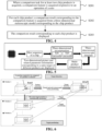
- FIG. 4 is a flowchart of a comparison method for a chip product according to an embodiment of the present disclosure. As shown in FIG. 4 , after the three-dimensional stereoscopic models corresponding to different chip products are obtained through the solution provided by the foregoing embodiments. The operations S201 to S203 are specifically included when the chip product is compared.
- a comparison solution of the chip products is implemented in a software system.
- the system includes a graphical user interface for interacting with a user, and also includes a database for storing data in a background, etc.
- the user may select and import three-dimensional stereoscopic models corresponding to different chips through the software system, or may directly select an identifier of the chip product to acquire the three-dimensional stereoscopic model.
- the user inputs a comparison feature through an operation.
- the comparison feature may be a certain position in the chip product, that is, the user may directly select the position in the three-dimensional stereoscopic model corresponding to the certain chip product.
- the system may acquire three-dimensional position coordinates of the selected position, and the three-dimensional position coordinates are taken as the comparison feature.
- the comparison feature also comprises parameter information of the chip product. The user may input a parameter required to be compared through an input box provided on the graphical user interface provided by the system, or different parameters may be directly displayed on the graphical user interface, and the user clicks to select the parameter required to be compared.
- the acquisition of the comparison feature at least includes the following two manners: a first manner of acquiring the three-dimensional position coordinates corresponding to a selected position, responsive to the position being selected by the user in the three-dimensional stereoscopic model of any one of the at least two chip products; and a second manner of receiving the parameter information of a chip product required to be compared input by the user.
- a comparison result corresponding to the comparison feature is acquired from the three-dimensional stereoscopic model corresponding to the chip product.
- the three-dimensional stereoscopic model corresponding to each chip product is a three-dimensional model which is recombined and constructed by using a neural network according to a slice sequence of the chip product.
- a specific modeling process refers to the foregoing embodiments.
- the system for comparing the chip products acquire other parameter features corresponding to the comparison feature, or position coordinates, or an image of a corresponding position from the three-dimensional stereoscopic model corresponding to each chip product as the comparison result. What content is contained in a specific comparison result is different according to the difference of the comparison feature.
- the comparison feature includes the three-dimensional position coordinates of the chip product required to be compared
- a process of acquiring the comparison result according to the three-dimensional stereoscopic model specifically includes that: for each chip product, a two-dimensional plane position is positioned in the three-dimensional stereoscopic model corresponding to the chip product according to the three-dimensional position coordinates. Then, a slice image corresponding to the two-dimensional plane position is acquired from a slice sequence corresponding to the chip product, and parameter information at the three-dimensional position coordinates is acquired from stored parameters of the chip product.
- the comparison result includes the slice image and the parameter information.
- the parameter information herein refers to parameters of the chip product itself, such as some parameters about devices and performance of the chip product.
- the two-dimensional plane position or the three-dimensional position coordinates may also be displayed in the graphical user interface, which is not limited by the solution.
- a process of acquiring the comparison result from the three-dimensional stereoscopic model corresponding to the chip product specifically includes that: for each chip product, the three-dimensional position coordinates corresponding to the parameter information are positioned in the three-dimensional stereoscopic model corresponding to the chip product; the two-dimensional plane position is positioned in the three-dimensional stereoscopic model corresponding to the chip product according to the three-dimensional position coordinates; and the slice image corresponding to the two-dimensional plane position is acquired from the slice sequence corresponding to the chip product.
- the comparison result includes the three-dimensional position coordinates and the slice image.
- a position of the parameter in the chip product may be positioned according to a certain parameter of the chip product, which may be used as the comparison result together with a specific slice image corresponding to the parameter.
- the parameter information of the chip product may also include other parameter information, which may also be displayed as the comparison result.
- the two-dimensional plane position or the three-dimensional position coordinates may also be displayed in the graphical user interface, which is not limited by the solution.
- the comparison result also includes at least one of the selected parameter information as the comparison feature, other parameter information or the two-dimensional plane position, etc.
- the specific implementation manner of positioning a two-dimensional position plane in the three-dimensional stereoscopic model according to the three-dimensional position coordinates may include that: the two-dimensional plane position corresponding to the three-dimensional position coordinates is positioned in the three-dimensional stereoscopic model corresponding to the chip product by adopting a neural network stereoscopic vision positioning,.
- the neural network stereoscopic vision positioning mainly includes that according to a stereoscopic vision principle, a nonlinear mapping relation is constructed between the three-dimensional coordinates and image coordinates of a space point by using the neural network, so that the system may realize one-to-one correspondence between a two-dimensional coordinates and a three-dimensional coordinates without complicated calibration of internal and external parameters of a camera, calibration and positioning calculation of a vision system are simplified.
- the method according to the present disclosure is more scientific and achieves a good effect on the accuracy of the positioning.
- the comparison result is displayed in the graphical user interface of a comparison system.
- the three-dimensional stereoscopic models of different chip products may be displayed, and at this time, the comparison result may be directly displayed in the three-dimensional stereoscopic model of the chip product and may also be independently displayed in a preset region for displaying comparison result. That is, the corresponding comparison result is displayed in the three-dimensional stereoscopic model corresponding to each chip product in the graphical user interface, or the comparison result corresponding to each chip product is displayed in the preset region for displaying comparison result.
- the chip product is modeled by the neural network based on the slice sequence of the chip product in advance to acquire the three-dimensional stereoscopic model.
- the comparison feature is acquired responsive to the operation of the user.
- the comparison result corresponding to the comparison feature is acquired from the three-dimensional stereoscopic model corresponding to each chip product. Then, the comparison result corresponding to each chip product is displayed.
- the core idea of the technical solution according to the present disclosure includes that a segmented sequence of a chip product is taken as an input, and three-dimensional stereoscopic structure of the chip product, that is, the three-dimensional stereoscopic model, is reconstructed by using a neural network method, so that the internal overall structure of the chip and related information thereof may be visually checked, and the problem that the specific position of an chip entity cannot be positioned is solved.
- any product is selected as a target group, and the other products are selected as a control group.
- the same target region is displayed in the control group through target automatic detection and positioning, and corresponding two-dimensional sequence image and related parameter information are displayed, so that the problems of the efficiency and accuracy of the parameter comparison are effectively solved.
- FIG. 5 is a schematic diagram of a modeling and comparison process of a chip product according to an embodiment of the present disclosure.
- each chip product is sliced in a certain manner (for example, the slicing is performed directly according to a certain interval to acquire the slice image, or the chip product is ground, and continuous images are acquired in a grinding process) to acquire a series of slice sequences.
- the slice sequence of each chip product is recombined by using the neural network, the three-dimensional stereoscopic structure is constructed to acquire three-dimensional stereoscopic model, and the three-dimensional model may be imported into the developed comparison system.
- any position of the three-dimensional stereoscopic model corresponding to any chip product is selected, and for the other products, a target region same as a region corresponding to the selected position may be automatically detected and positioned, and a corresponding two-dimensional picture (that is, the slice image) and a specific related parameter are displayed.
- FIG. 6 is a schematic diagram of a comparison of a chip product according to an embodiment of the present disclosure. As shown in FIG. 6 , a specific manner of comparing multiple chip products is shown. A product 1 is taken as the target group, and a user may manually select a position required to be compared in the product 1. The position may be represented by the three-dimensional position coordinates (x, y, z). The comparison system performs feature extraction on the position; target detection is performed by adopting the neural network stereoscopic vision positioning; the two-dimensional plane position (x1, y1) corresponding to the selected position is positioned; and then, the same target positions in other product 2, ... , and product n are automatically positioned.
- the slice image and parameter information of different chip products at the position may be acquired through the two-dimensional plane position and the acquired slice image and the parameter information are taken as the comparison result of the comparison of the chip product this time.
- the same target region is automatically detected and positioned in other products, and the two-dimensional picture and the parameter information corresponding to each product are displayed, so that the comparison is implemented rapidly.
- the two-dimensional plane position (x1, y1) in the product 1 may be selected, and when detecting that the parameter information corresponding to the two-dimensional plane position (x1, y1) contains a structure name, the two-dimensional picture related to the structure name corresponding to each product may be displayed.
- the modeling method and comparison method for a chip product by reconstructing the three-dimensional structure of the chip product, an internal parameter and structure of each chip product may be visually checked. Furthermore, when the chip products are compared, a target automatic detection and positioning method is used, so that the same target region in each chip product is displayed simultaneously, and the efficiency and accuracy of the comparison are effectively improved. Furthermore, in a comparison process, a region in the three-dimensional stereoscopic model corresponding to any chip product is selected, the target group and the control group may have their corresponding two-dimensional pictures and corresponding related specific parameter information displayed, so that the difference of the same parameter among the products may be visually compared and checked.
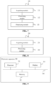
- FIG. 7 is a schematic structural diagram of a comparison device for a chip product according to an embodiment not being part of the invention.
- the comparison device 10 for a chip product includes an acquiring module 11, a processing module 12, and a displaying module 13.
- the processing module 12 is configured to, for each chip product, acquire a comparison result corresponding to the comparison feature from a three-dimensional stereoscopic model corresponding to the chip product.
- the three-dimensional stereoscopic model corresponding to each chip product is a three-dimensional model which is recombined and constructed by using a neural network according to a slice sequence of the chip product.
- the displaying module 13 is configured to display the comparison result corresponding to each chip product.
- the comparison feature includes three-dimensional position coordinates or parameter information of the chip product required to be compared.
- the acquiring module 11 is specifically configured to execute the following operation.
- the three-dimensional position coordinates corresponding to the selected position are acquired.
- the comparison feature includes the three-dimensional position coordinates of the chip product required to be compared.
- the processing module 12 is specifically configured to perform the following operations.
- a two-dimensional plane position is positioned in the three-dimensional stereoscopic model corresponding to the chip product according to the three-dimensional position coordinates.
- a slice image corresponding to the two-dimensional plane position is acquired from the slice sequence corresponding to the chip product.
- Parameter information at the three-dimensional position coordinates is acquired from stored parameters of the chip product.
- the comparison result includes the slice image and the parameter information.
- the comparison feature includes the parameter information of the chip product required to be compared.
- the processing module 12 is specifically configured to perform the following operations.
- the three-dimensional position coordinates corresponding to the parameter information are positioned in the three-dimensional stereoscopic model corresponding to the chip product.
- the two-dimensional plane position is positioned in the three-dimensional stereoscopic model corresponding to the chip product according to the three-dimensional position coordinates.
- a slice image corresponding to the two-dimensional plane position is acquired from the slice sequence corresponding to the chip product.
- the comparison result includes the three-dimensional position coordinates and the slice image.
- the comparison result further includes at least one of the parameter information or the two-dimensional plane position.
- processing module 12 is specifically configured to perform the following operation.
- the two-dimensional plane position corresponding to the three-dimensional position coordinates is positioned in the three-dimensional stereoscopic model corresponding to the chip product by adopting a neural network stereoscopic vision positioning.
- the displaying module 13 is specifically configured to perform the following operation.
- the corresponding comparison result is displayed in the three-dimensional stereoscopic model corresponding to each chip product in a graphical user interface.
- the comparison result corresponding to each chip product is displayed in a preset region for displaying the comparison result in the graphical user interface.
- comparison device for a chip product provided by any foregoing embodiments and the technical solutions for implementing the comparison method for a chip product in the foregoing embodiments are similar in implementation principle and technical effect, which will not be described in detail herein.
- FIG. 8 is a schematic structural diagram of a modeling device for a chip product according to an embodiment not being part of the invention.
- the modeling device 20 of a chip product includes an acquiring module 21 and a processing module 22.
- the acquiring module 21 is configured to acquire a slice sequence of a to-be-modeled chip product.
- the slice sequence includes multiple continuous slice images acquired by slicing the chip product.
- the processing module 22 is configured to, according to the slice sequence, perform recombination and construction by using a neural network to acquire a three-dimensional stereoscopic model corresponding to the chip product.
- the three-dimensional stereoscopic model is used for comparison of parameter information and the slice image between chip products when the chip products are compared.
- the neural network includes a residual network, a U-net network model and a multi-granularity network model.
- the processing module 22 is specifically configured to perform the following operations.
- Each slice image in the slice sequence is input into the residual network for feature extraction to acquire a first image feature of each slice image.
- the slice sequence is segmented through the U-net network model.
- Each slice image in the segmented slice sequence is input into the residual network for feature extraction to acquire a second image feature of each slice image.
- the first image feature and the second image feature of each slice image are merged to acquire an image feature of the slice image.
- the three-dimensional stereoscopic model corresponding to the chip product is constructed by adopting the multi-granularity network model according to the slice sequence and the image feature of each slice image.
- processing module 22 is specifically configured to perform the following operation.
- a grid-shaped three-dimensional geometric shape is generated according to multiple slice images in the slice sequence by adopting the multi-granularity network model and by taking a center of the chip product as the center of a three-dimensional coordinate system.
- the image feature of each slice image is embedded into the three-dimensional geometric shape and the training is performed to obtain the three-dimensional stereoscopic model.
- the image feature of each slice image in the slice sequence includes: a structural feature in the slice image and information about correlation between the slice image and preceding and following images of the slice image in the slice sequence.
- the modeling device for a chip product provided by any foregoing embodiments and the technical solutions for implementing the modeling method for a chip product in the foregoing embodiments are similar in implementation principle and technical effect, which will not be described in detail herein.
- FIG. 9 is a schematic structural diagram of an electronic apparatus device according to an embodiment of the present disclosure.
- the electronic device 30 includes: a processor 31 and a memory 32.
- the electronic device may also include a display 33 and a bus 34 for connecting elements.
- the memory 32 is configured to store a computer program.
- the processor 31 calls the computer program stored in the memory 32 to perform the technical solutions in any method embodiment.
- the memory 32 may be independent and may also be integrated with the processor 31.
- the present invention further provides a computer-readable storage medium.
- the computer-readable storage medium stores a computer program.
- the processor is enabled to perform the technical solutions in any method embodiment.
- the processor mentioned in the embodiments of the present disclosure may be a Central Processing Unit (CPU), and may also be other general purpose processor, a Digital Signal Processor (DSP), an Application Specific Integrated Circuit (ASIC), a Field Programmable Gate Array (FPGA) or other programmable logic device, a discrete gate or a transistor logic device, a discrete hardware component, etc.
- the general purpose processor may be a microprocessor or the processor may also be any conventional processor, etc.
- the memory mentioned in the embodiment of the present disclosure may be a volatile memory or a nonvolatile memory, or may include both the volatile memory and the nonvolatile memory.
- the nonvolatile memory may be a Read-Only Memory (ROM), a Programmable ROM (PROM), an Erasable PROM (EPROM), and an Electrically PROM (EEPROM), or a flash memory.
- the volatile memory may be a Random Access Memory (RAM), which is used as an external cache.
- RAM Direct Rambus RAM
- SRAM Static RAM
- DRAM Dynamic RAM
- SDRAM Synchronous DRAM
- DDR SDRAM Double Data Rate Synchronous DRAM
- ESDRAM Enhanced SDRAM
- SLDRAM Synchlink DRAM
- DR RAM Direct Rambus RAM
- the processor is the general purpose processor, the DSP, the ASIC, the FPGA or other programmable logic device, the discrete gate or transistor logic device, or the discrete hardware component, the memory (a storage module) is integrated into the processor.
Landscapes
- Engineering & Computer Science (AREA)
- Theoretical Computer Science (AREA)
- Physics & Mathematics (AREA)
- General Physics & Mathematics (AREA)
- Software Systems (AREA)
- Evolutionary Computation (AREA)
- Computer Vision & Pattern Recognition (AREA)
- General Engineering & Computer Science (AREA)
- Artificial Intelligence (AREA)
- Health & Medical Sciences (AREA)
- General Health & Medical Sciences (AREA)
- Computing Systems (AREA)
- Multimedia (AREA)
- Computer Hardware Design (AREA)
- Computer Graphics (AREA)
- Geometry (AREA)
- Databases & Information Systems (AREA)
- Medical Informatics (AREA)
- Life Sciences & Earth Sciences (AREA)
- Mathematical Physics (AREA)
- Biomedical Technology (AREA)
- Molecular Biology (AREA)
- Biophysics (AREA)
- Computational Linguistics (AREA)
- Data Mining & Analysis (AREA)
- Quality & Reliability (AREA)
- Radar, Positioning & Navigation (AREA)
- Remote Sensing (AREA)
- Image Analysis (AREA)
Claims (12)
- Vergleichsverfahren für ein Chipprodukt, das Verfahren umfassend:Erfassen einer Vergleichsaufgabe, die in einem Softwaresystem für mindestens zwei Chipprodukte implementiert ist, und Erfassen eines Vergleichsmerkmals als Reaktion auf eine Bedienung eines Benutzers (S201), wobei das Vergleichsmerkmal dreidimensionale Positionskoordinaten und Parameterinformationen über die zu vergleichenden Chipprodukte umfasst;für jedes Chipprodukt, Erfassen eines Vergleichsresultats, das dem Vergleichsmerkmal entspricht, von einem dreidimensionalen stereoskopischen Modell, das dem Chipprodukt entspricht (S202), wobei das Vergleichsresultat Schichtbilder und die Parameterinformationen des Chipprodukts umfasst,
wobei das dreidimensionale stereoskopische Modell, das jedem Chipprodukt entspricht, ein dreidimensionales Modell ist, das durch ein neuronales Netz gemäß einer Schichtsequenz des Chipprodukts rekombiniert und konstruiert wird, wobei das neuronale Netz ein Restnetz, ein U-Netz-Netzmodell und ein Multigranularität-Netzmodell umfasst, wobei die Schichtsequenz eine Vielzahl von kontinuierlichen Schichtbildern umfasst, die durch Schneiden des Chipprodukts erfasst werden, und wobei ein Bildmerkmal von jedem Schichtbild in eine dreidimensionale geometrische Form eingebettet ist, um das dreidimensionale stereoskopische Modell zu erlangen; undanzeigen des Vergleichsresultats, das jedem Chipprodukt (S203) entspricht, so dass der gleiche Zielbereich in jedem Chipprodukt gleichzeitig angezeigt wird;wobei das dreidimensionale stereoskopische Modell, das dem Chipprodukt entspricht, durch Folgendes erfasst wird: Eingeben von jedem Schichtbild in der Schichtsequenz in das Restnetz, um einer Merkmalsextraktion unterzogen zu werden, um ein erstes Bildmerkmal von jedem Schichtbilds zu erlangen; Segmentieren der Schichtsequenz durch das U-Netz-Netzmodell, und Eingeben von jedem Schichtbild in der segmentierten Schichtsequenz in das Restnetz, um einer Merkmalsextraktion unterzogen zu werden, um ein zweites Bildmerkmal von jedem Schichtbild zu erlangen; Verschmelzen des ersten Bildmerkmals und des zweiten Bildmerkmals von jedem Schichtbild, um ein Bildmerkmal des Schichtbilds zu erlangen; und Konstruieren des dreidimensionalen stereoskopischen Modells, das dem Chipprodukt entspricht, durch Annehmen des Multigranularität-Netzmodells gemäß der Schichtsequenz und dem Bildmerkmal von jedem Schichtbild;wobei das Bildmerkmal mindestens eines von Farbmerkmalen, Texturmerkmalen, Formmerkmalen und Tiefenmerkmalen beinhaltet. - Verfahren nach Anspruch 1, wobei ein Erfassen des Vergleichsmerkmals als Reaktion auf die Bedienung des Benutzers Folgendes umfasst:als Reaktion auf die Auswahl einer Position durch den Benutzer in dem dreidimensionalen stereoskopischen Modell eines der mindestens zwei Chipprodukte, Erfassen der dreidimensionalen Positionskoordinaten, die der ausgewählten Position entsprechen;
oderEmpfangen der von dem Benutzer eingegebenen Parameterinformationen des zu vergleichenden Chipprodukts. - Verfahren nach Anspruch 2, wobei das Vergleichsmerkmal die dreidimensionalen Positionskoordinaten des zu vergleichenden Chipprodukts umfasst; und für jedes Chipprodukt das Erfassen des dem Vergleichsmerkmal entsprechenden Vergleichsresultats aus dem dem Chipprodukt entsprechenden dreidimensionalen stereoskopischen Modell umfasst:für jedes Chipprodukt, Positionieren einer zweidimensionalen Ebenenposition in dem dreidimensionalen stereoskopischen Modell entsprechend dem Chipprodukt gemäß den dreidimensionalen Positionskoordinaten;Erfassen eines der zweidimensionalen Ebenenposition entsprechenden Schichtbilds aus der dem Chipprodukt entsprechenden Schichtsequenz; undErfassen von Parameterinformationen an den dreidimensionalen Positionskoordinaten anhand von gespeicherten Parametern des Chipprodukts.
- Verfahren nach Anspruch 2, wobei das Vergleichsmerkmal die Parameterinformationen des zu vergleichenden Chipprodukts umfasst; und für jedes Chipprodukt Erfassen des dem Vergleichsmerkmal entsprechenden Vergleichsresultats aus dem dem Chipprodukt entsprechenden dreidimensionalen stereoskopischen Modell Folgendes umfasst:für jedes Chipprodukt, Positionieren der dreidimensionalen Positionskoordinaten, die den Parameterinformationen in dem dreidimensionalen stereoskopischen Modell entsprechen, das dem Chipprodukt entspricht;Positionieren einer zweidimensionalen Ebenenposition in dem dreidimensionalen stereoskopischen Modell entsprechend dem Chipprodukt gemäß den dreidimensionalen Positionskoordinaten; undErfassen eines der zweidimensionalen Ebenenposition entsprechenden Schichtbilds aus der dem Chipprodukt entsprechenden Schichtsequenz,wobei das Vergleichsresultat die dreidimensionalen Positionskoordinaten und das Schichtbild umfasst.
- Verfahren nach Anspruch 4, wobei das Vergleichsresultat ferner mindestens eines von den Parameterinformationen oder der zweidimensionalen Ebenenposition umfasst.
- Verfahren nach einem der Ansprüche 3 bis 5, wobei ein Positionieren einer zweidimensionalen Ebenenposition in dem dreidimensionalen stereoskopischen Modell entsprechend dem Chipprodukt gemäß den dreidimensionalen Positionskoordinaten Folgendes umfasst:
Positionieren der zweidimensionalen Ebenenposition, die den dreidimensionalen Positionskoordinaten in dem dreidimensionalen stereoskopischen Modell entspricht, das dem Chipprodukt entspricht, durch Anwenden eines Positionierens des stereoskopischen Sehens über neuronales Netz. - Verfahren nach einem der Ansprüche 1 bis 5, wobei ein Anzeigen des Vergleichsresultats für jedes Chipprodukt Folgendes umfasst:Anzeigen des entsprechenden Vergleichsresultats in dem dreidimensionalen stereoskopischen Modell, das jedem Chipprodukt entspricht, in einer grafischen Benutzeroberfläche;
oderAnzeigen des Vergleichsresultats, das jedem Chipprodukt entspricht, in einem voreingestellten Bereich zum Anzeigen des Vergleichsresultats in der grafischen Benutzeroberfläche. - Verfahren nach einem der Ansprüche 1 bis 7, wobei das Chipprodukt durch die folgenden Vorgänge modelliert ist:Erfassen einer Schichtsequenz eines zu modellierenden Chipprodukts (S101); undDurchführen, gemäß der Schnittsequenz, von Rekombination und Konstruktion unter Verwendung des neuronalen Netzes, um das dreidimensionale stereoskopische Modell zu erlangen, das dem Chipprodukt entspricht (S102), wobei das dreidimensionale stereoskopische Modell zum Vergleich von Parameterinformationen und dem Schnittbild zwischen Chipprodukten verwendet wird, wenn die Chipprodukte verglichen werden.
- Verfahren nach Anspruch 8, wobei ein Konstruieren des dreidimensionalen stereoskopischen Modells, das dem Chipprodukt entspricht, durch Verwendung des Multigranularität-Netzmodells gemäß der Schichtsequenz und dem Bildmerkmal jedes Schichtbilds Folgendes umfasst;Erzeugen einer gitterförmigen dreidimensionalen geometrischen Form gemäß einer Vielzahl von Schichtbildern in der Schichtsequenz, indem das Multigranularität-Netzmodell angewendet wird und indem eine Mitte des Chipprodukts als Mitte eines dreidimensionalen Koordinatensystems genommen wird; undEinbetten des Bildmerkmals von jedem Schichtbild in die dreidimensionale geometrische Form, und Erfassen des dreidimensionalen stereoskopischen Modells durch Anwenden des Multigranularität-Netzmodells basierend auf dem mit dem Bildmerkmal eingebetteten dreidimensionalen geometrischen Form.
- Verfahren nach Anspruch 1, wobei das Bildmerkmal von jedem Schichtbild in der Schichtsequenz Folgendes umfasst: ein Strukturmerkmal in dem Schichtbild und Informationen über die Korrelation zwischen dem Schichtbild und vorhergehenden und nachfolgenden Bildern des Schichtbilds in der Schichtsequenz.
- Elektronische Vorrichtung (30), umfassend:einen Prozessor (31) und einen Speicher (32),dadurch gekennzeichnet, dass der Speicher (32) konfiguriert ist, um ein Computerprogramm zu speichern, und der Prozessor (31) das in dem Speicher (32) gespeicherte Computerprogramm aufruft, um das Verfahren nach einem der Ansprüche 1 bis 10 durchzuführen.
- Computerlesbares Speichermedium, auf dem ein Computerprogramm gespeichert ist, das, wenn es von einem Prozessor ausgeführt wird, den Prozessor veranlasst, das Verfahren nach einem der Ansprüche 1 bis 10 durchzuführen.
Applications Claiming Priority (2)
| Application Number | Priority Date | Filing Date | Title |
|---|---|---|---|
| CN202011010056.7A CN114254584B (zh) | 2020-09-23 | 2020-09-23 | 芯片产品的对比方法、建模方法、装置及存储介质 |
| PCT/CN2021/097394 WO2022062466A1 (zh) | 2020-09-23 | 2021-05-31 | 芯片产品的对比方法、建模方法、装置及存储介质 |
Publications (3)
| Publication Number | Publication Date |
|---|---|
| EP4053729A1 EP4053729A1 (de) | 2022-09-07 |
| EP4053729A4 EP4053729A4 (de) | 2023-06-07 |
| EP4053729B1 true EP4053729B1 (de) | 2025-04-23 |
Family
ID=80741672
Family Applications (1)
| Application Number | Title | Priority Date | Filing Date |
|---|---|---|---|
| EP21844610.2A Active EP4053729B1 (de) | 2020-09-23 | 2021-05-31 | Verfahren und vorrichtung zum vergleichen von chipprodukten, verfahren und vorrichtung zum modellieren von chipprodukten und speichermedium |
Country Status (2)
| Country | Link |
|---|---|
| US (1) | US11854186B2 (de) |
| EP (1) | EP4053729B1 (de) |
Families Citing this family (1)
| Publication number | Priority date | Publication date | Assignee | Title |
|---|---|---|---|---|
| CN117078936B (zh) * | 2023-08-29 | 2025-11-25 | 光力瑞弘电子科技有限公司 | 一种模型自动学习方法、装置、划片机及介质 |
Family Cites Families (13)
| Publication number | Priority date | Publication date | Assignee | Title |
|---|---|---|---|---|
| US5461709A (en) * | 1993-02-26 | 1995-10-24 | Intergraph Corporation | 3D input system for CAD systems |
| US7937179B2 (en) * | 2007-05-24 | 2011-05-03 | Applied Materials, Inc. | Dynamic inline yield analysis and prediction of a defect limited yield using inline inspection defects |
| CN104101330B (zh) | 2014-06-23 | 2017-01-11 | 中国科学院半导体研究所 | 一种基于空间差分整形的距离选通超分辨率三维成像方法 |
| CN105701263A (zh) | 2014-11-26 | 2016-06-22 | 英业达科技有限公司 | 三维模型零件比对系统及其方法 |
| KR20180072768A (ko) * | 2015-10-19 | 2018-06-29 | 에이에스엠엘 네델란즈 비.브이. | 패터닝 공정 오차를 보정하는 장치 및 방법 |
| JP6827906B2 (ja) | 2017-10-30 | 2021-02-10 | 株式会社日立ビルシステム | 三次元データ処理装置及び三次元データ処理方法 |
| CN108038874B (zh) | 2017-12-01 | 2020-07-24 | 中国科学院自动化研究所 | 面向序列切片的扫描电镜图像实时配准装置及方法 |
| US11199506B2 (en) * | 2018-02-21 | 2021-12-14 | Applied Materials Israel Ltd. | Generating a training set usable for examination of a semiconductor specimen |
| KR102499656B1 (ko) * | 2018-02-23 | 2023-02-14 | 에이에스엠엘 네델란즈 비.브이. | 패턴의 시맨틱 분할을 위한 딥 러닝 |
| CN109685147B (zh) | 2018-12-27 | 2023-08-11 | 武汉益模科技股份有限公司 | 一种基于三维模型的差异性对比方法 |
| CN110133014B (zh) * | 2019-04-25 | 2022-07-05 | 合刃科技(深圳)有限公司 | 一种芯片内部缺陷检测方法及系统 |
| EP4031833A2 (de) * | 2019-09-18 | 2022-07-27 | inveox GmbH | System und verfahren zum erzeugen eines 3d-modells einer pathologischen probe |
| US20200027021A1 (en) * | 2019-09-27 | 2020-01-23 | Kumara Sastry | Reinforcement learning for multi-domain problems |
-
2021
- 2021-05-31 EP EP21844610.2A patent/EP4053729B1/de active Active
- 2021-07-30 US US17/389,735 patent/US11854186B2/en active Active
Also Published As
| Publication number | Publication date |
|---|---|
| US20220092759A1 (en) | 2022-03-24 |
| US11854186B2 (en) | 2023-12-26 |
| EP4053729A1 (de) | 2022-09-07 |
| EP4053729A4 (de) | 2023-06-07 |
Similar Documents
| Publication | Publication Date | Title |
|---|---|---|
| CN114254584B (zh) | 芯片产品的对比方法、建模方法、装置及存储介质 | |
| CN110852949B (zh) | 点云数据补全方法、装置、计算机设备和存储介质 | |
| US9811760B2 (en) | Online per-feature descriptor customization | |
| CN110827202A (zh) | 目标检测方法、装置、计算机设备和存储介质 | |
| WO2016068869A1 (en) | Three dimensional object recognition | |
| CN113673530A (zh) | 遥感图像语义分割方法、装置、计算机设备和存储介质 | |
| CN111753031B (zh) | 地图区域的整合方法、装置、存储介质和电子设备 | |
| CN110110726A (zh) | 电力设备铭牌识别方法、装置、计算机设备和存储介质 | |
| US20240070979A1 (en) | Method and apparatus for generating 3d spatial information | |
| CN108304243B (zh) | 界面生成方法、装置、计算机设备和存储介质 | |
| CN111639523A (zh) | 目标检测方法、装置、计算机设备和存储介质 | |
| CN111178202A (zh) | 目标检测方法、装置、计算机设备和存储介质 | |
| US11854186B2 (en) | Comparison method and modeling method for chip product, device and storage medium | |
| KR20150099964A (ko) | 이미지 특징 추출 장치 및 방법 | |
| CN112508064A (zh) | 指静脉身份识别方法、装置、计算机设备和存储介质 | |
| CN110490020B (zh) | 条码识别方法、装置、计算机设备和存储介质 | |
| CN110991473A (zh) | 图像样本的特征选择方法、装置、计算机设备及存储介质 | |
| CN111552751A (zh) | 三维地标控制点生成及应用方法、生成及应用装置 | |
| CN111476308B (zh) | 基于先验几何约束的遥感影像分类方法、装置和电子设备 | |
| CN111274421B (zh) | 图片数据清洗方法、装置、计算机设备和存储介质 | |
| CN116881515B (zh) | 对不同算法求解的电容结果进行比较的方法及电子设备 | |
| CN111143412A (zh) | 数据对比方法、装置、计算机及计算机可读存储介质 | |
| CN114578961B (zh) | 基于动作录制的数据自动化录入系统 | |
| CN111626288A (zh) | 数据处理方法、装置、计算机设备和存储介质 | |
| CN112184742A (zh) | 图形共边检测方法、装置、设备及计算机可读介质 |
Legal Events
| Date | Code | Title | Description |
|---|---|---|---|
| STAA | Information on the status of an ep patent application or granted ep patent |
Free format text: STATUS: UNKNOWN |
|
| STAA | Information on the status of an ep patent application or granted ep patent |
Free format text: STATUS: THE INTERNATIONAL PUBLICATION HAS BEEN MADE |
|
| PUAI | Public reference made under article 153(3) epc to a published international application that has entered the european phase |
Free format text: ORIGINAL CODE: 0009012 |
|
| STAA | Information on the status of an ep patent application or granted ep patent |
Free format text: STATUS: REQUEST FOR EXAMINATION WAS MADE |
|
| 17P | Request for examination filed |
Effective date: 20220127 |
|
| AK | Designated contracting states |
Kind code of ref document: A1 Designated state(s): AL AT BE BG CH CY CZ DE DK EE ES FI FR GB GR HR HU IE IS IT LI LT LU LV MC MK MT NL NO PL PT RO RS SE SI SK SM TR |
|
| A4 | Supplementary search report drawn up and despatched |
Effective date: 20230509 |
|
| RIC1 | Information provided on ipc code assigned before grant |
Ipc: G06F 30/27 20200101ALI20230502BHEP Ipc: G06V 10/82 20220101ALI20230502BHEP Ipc: G06N 3/02 20060101ALI20230502BHEP Ipc: G06T 17/00 20060101ALI20230502BHEP Ipc: G06F 30/398 20200101AFI20230502BHEP |
|
| STAA | Information on the status of an ep patent application or granted ep patent |
Free format text: STATUS: EXAMINATION IS IN PROGRESS |
|
| DAV | Request for validation of the european patent (deleted) | ||
| DAX | Request for extension of the european patent (deleted) | ||
| 17Q | First examination report despatched |
Effective date: 20231211 |
|
| GRAP | Despatch of communication of intention to grant a patent |
Free format text: ORIGINAL CODE: EPIDOSNIGR1 |
|
| STAA | Information on the status of an ep patent application or granted ep patent |
Free format text: STATUS: GRANT OF PATENT IS INTENDED |
|
| INTG | Intention to grant announced |
Effective date: 20250210 |
|
| GRAS | Grant fee paid |
Free format text: ORIGINAL CODE: EPIDOSNIGR3 |
|
| GRAA | (expected) grant |
Free format text: ORIGINAL CODE: 0009210 |
|
| STAA | Information on the status of an ep patent application or granted ep patent |
Free format text: STATUS: THE PATENT HAS BEEN GRANTED |
|
| P01 | Opt-out of the competence of the unified patent court (upc) registered |
Free format text: CASE NUMBER: APP_11403/2025 Effective date: 20250308 |
|
| AK | Designated contracting states |
Kind code of ref document: B1 Designated state(s): AL AT BE BG CH CY CZ DE DK EE ES FI FR GB GR HR HU IE IS IT LI LT LU LV MC MK MT NL NO PL PT RO RS SE SI SK SM TR |
|
| REG | Reference to a national code |
Ref country code: GB Ref legal event code: FG4D |
|
| REG | Reference to a national code |
Ref country code: CH Ref legal event code: EP |
|
| REG | Reference to a national code |
Ref country code: DE Ref legal event code: R096 Ref document number: 602021029762 Country of ref document: DE |
|
| REG | Reference to a national code |
Ref country code: IE Ref legal event code: FG4D |
|
| PGFP | Annual fee paid to national office [announced via postgrant information from national office to epo] |
Ref country code: DE Payment date: 20250521 Year of fee payment: 5 |
|
| REG | Reference to a national code |
Ref country code: NL Ref legal event code: MP Effective date: 20250423 |
|
| PG25 | Lapsed in a contracting state [announced via postgrant information from national office to epo] |
Ref country code: NL Free format text: LAPSE BECAUSE OF FAILURE TO SUBMIT A TRANSLATION OF THE DESCRIPTION OR TO PAY THE FEE WITHIN THE PRESCRIBED TIME-LIMIT Effective date: 20250423 |
|
| REG | Reference to a national code |
Ref country code: AT Ref legal event code: MK05 Ref document number: 1788486 Country of ref document: AT Kind code of ref document: T Effective date: 20250423 |
|
| PG25 | Lapsed in a contracting state [announced via postgrant information from national office to epo] |
Ref country code: FI Free format text: LAPSE BECAUSE OF FAILURE TO SUBMIT A TRANSLATION OF THE DESCRIPTION OR TO PAY THE FEE WITHIN THE PRESCRIBED TIME-LIMIT Effective date: 20250423 Ref country code: ES Free format text: LAPSE BECAUSE OF FAILURE TO SUBMIT A TRANSLATION OF THE DESCRIPTION OR TO PAY THE FEE WITHIN THE PRESCRIBED TIME-LIMIT Effective date: 20250423 Ref country code: PT Free format text: LAPSE BECAUSE OF FAILURE TO SUBMIT A TRANSLATION OF THE DESCRIPTION OR TO PAY THE FEE WITHIN THE PRESCRIBED TIME-LIMIT Effective date: 20250825 |
|
| REG | Reference to a national code |
Ref country code: LT Ref legal event code: MG9D |
|
| PG25 | Lapsed in a contracting state [announced via postgrant information from national office to epo] |
Ref country code: GR Free format text: LAPSE BECAUSE OF FAILURE TO SUBMIT A TRANSLATION OF THE DESCRIPTION OR TO PAY THE FEE WITHIN THE PRESCRIBED TIME-LIMIT Effective date: 20250724 Ref country code: NO Free format text: LAPSE BECAUSE OF FAILURE TO SUBMIT A TRANSLATION OF THE DESCRIPTION OR TO PAY THE FEE WITHIN THE PRESCRIBED TIME-LIMIT Effective date: 20250723 |
|
| PG25 | Lapsed in a contracting state [announced via postgrant information from national office to epo] |
Ref country code: PL Free format text: LAPSE BECAUSE OF FAILURE TO SUBMIT A TRANSLATION OF THE DESCRIPTION OR TO PAY THE FEE WITHIN THE PRESCRIBED TIME-LIMIT Effective date: 20250423 |
|
| PG25 | Lapsed in a contracting state [announced via postgrant information from national office to epo] |
Ref country code: BG Free format text: LAPSE BECAUSE OF FAILURE TO SUBMIT A TRANSLATION OF THE DESCRIPTION OR TO PAY THE FEE WITHIN THE PRESCRIBED TIME-LIMIT Effective date: 20250423 |
|
| PG25 | Lapsed in a contracting state [announced via postgrant information from national office to epo] |
Ref country code: HR Free format text: LAPSE BECAUSE OF FAILURE TO SUBMIT A TRANSLATION OF THE DESCRIPTION OR TO PAY THE FEE WITHIN THE PRESCRIBED TIME-LIMIT Effective date: 20250423 |
|
| PG25 | Lapsed in a contracting state [announced via postgrant information from national office to epo] |
Ref country code: AT Free format text: LAPSE BECAUSE OF FAILURE TO SUBMIT A TRANSLATION OF THE DESCRIPTION OR TO PAY THE FEE WITHIN THE PRESCRIBED TIME-LIMIT Effective date: 20250423 |
|
| PG25 | Lapsed in a contracting state [announced via postgrant information from national office to epo] |
Ref country code: RS Free format text: LAPSE BECAUSE OF FAILURE TO SUBMIT A TRANSLATION OF THE DESCRIPTION OR TO PAY THE FEE WITHIN THE PRESCRIBED TIME-LIMIT Effective date: 20250723 |
|
| PG25 | Lapsed in a contracting state [announced via postgrant information from national office to epo] |
Ref country code: IS Free format text: LAPSE BECAUSE OF FAILURE TO SUBMIT A TRANSLATION OF THE DESCRIPTION OR TO PAY THE FEE WITHIN THE PRESCRIBED TIME-LIMIT Effective date: 20250823 |
|
| PG25 | Lapsed in a contracting state [announced via postgrant information from national office to epo] |
Ref country code: LV Free format text: LAPSE BECAUSE OF FAILURE TO SUBMIT A TRANSLATION OF THE DESCRIPTION OR TO PAY THE FEE WITHIN THE PRESCRIBED TIME-LIMIT Effective date: 20250423 |
|
| REG | Reference to a national code |
Ref country code: CH Ref legal event code: H13 Free format text: ST27 STATUS EVENT CODE: U-0-0-H10-H13 (AS PROVIDED BY THE NATIONAL OFFICE) Effective date: 20251223 |
|
| PG25 | Lapsed in a contracting state [announced via postgrant information from national office to epo] |
Ref country code: SM Free format text: LAPSE BECAUSE OF FAILURE TO SUBMIT A TRANSLATION OF THE DESCRIPTION OR TO PAY THE FEE WITHIN THE PRESCRIBED TIME-LIMIT Effective date: 20250423 Ref country code: DK Free format text: LAPSE BECAUSE OF FAILURE TO SUBMIT A TRANSLATION OF THE DESCRIPTION OR TO PAY THE FEE WITHIN THE PRESCRIBED TIME-LIMIT Effective date: 20250423 |
|
| PG25 | Lapsed in a contracting state [announced via postgrant information from national office to epo] |
Ref country code: LU Free format text: LAPSE BECAUSE OF NON-PAYMENT OF DUE FEES Effective date: 20250531 |
|
| PG25 | Lapsed in a contracting state [announced via postgrant information from national office to epo] |
Ref country code: CH Free format text: LAPSE BECAUSE OF NON-PAYMENT OF DUE FEES Effective date: 20250531 |
|
| PG25 | Lapsed in a contracting state [announced via postgrant information from national office to epo] |
Ref country code: CZ Free format text: LAPSE BECAUSE OF FAILURE TO SUBMIT A TRANSLATION OF THE DESCRIPTION OR TO PAY THE FEE WITHIN THE PRESCRIBED TIME-LIMIT Effective date: 20250423 |
|
| PG25 | Lapsed in a contracting state [announced via postgrant information from national office to epo] |
Ref country code: EE Free format text: LAPSE BECAUSE OF FAILURE TO SUBMIT A TRANSLATION OF THE DESCRIPTION OR TO PAY THE FEE WITHIN THE PRESCRIBED TIME-LIMIT Effective date: 20250423 |
|
| REG | Reference to a national code |
Ref country code: DE Ref legal event code: R097 Ref document number: 602021029762 Country of ref document: DE |
|
| PG25 | Lapsed in a contracting state [announced via postgrant information from national office to epo] |
Ref country code: SK Free format text: LAPSE BECAUSE OF FAILURE TO SUBMIT A TRANSLATION OF THE DESCRIPTION OR TO PAY THE FEE WITHIN THE PRESCRIBED TIME-LIMIT Effective date: 20250423 |
|
| PG25 | Lapsed in a contracting state [announced via postgrant information from national office to epo] |
Ref country code: IT Free format text: LAPSE BECAUSE OF FAILURE TO SUBMIT A TRANSLATION OF THE DESCRIPTION OR TO PAY THE FEE WITHIN THE PRESCRIBED TIME-LIMIT Effective date: 20250423 |
|
| REG | Reference to a national code |
Ref country code: BE Ref legal event code: MM Effective date: 20250531 |
|
| PG25 | Lapsed in a contracting state [announced via postgrant information from national office to epo] |
Ref country code: MC Free format text: LAPSE BECAUSE OF FAILURE TO SUBMIT A TRANSLATION OF THE DESCRIPTION OR TO PAY THE FEE WITHIN THE PRESCRIBED TIME-LIMIT Effective date: 20250423 |
|
| PG25 | Lapsed in a contracting state [announced via postgrant information from national office to epo] |
Ref country code: RO Free format text: LAPSE BECAUSE OF FAILURE TO SUBMIT A TRANSLATION OF THE DESCRIPTION OR TO PAY THE FEE WITHIN THE PRESCRIBED TIME-LIMIT Effective date: 20250423 |
|
| PLBE | No opposition filed within time limit |
Free format text: ORIGINAL CODE: 0009261 |
|
| STAA | Information on the status of an ep patent application or granted ep patent |
Free format text: STATUS: NO OPPOSITION FILED WITHIN TIME LIMIT |
|
| REG | Reference to a national code |
Ref country code: CH Ref legal event code: L10 Free format text: ST27 STATUS EVENT CODE: U-0-0-L10-L00 (AS PROVIDED BY THE NATIONAL OFFICE) Effective date: 20260304 |
|
| GBPC | Gb: european patent ceased through non-payment of renewal fee |
Effective date: 20250723 |
|
| 26N | No opposition filed |
Effective date: 20260126 |
|
| PG25 | Lapsed in a contracting state [announced via postgrant information from national office to epo] |
Ref country code: GB Free format text: LAPSE BECAUSE OF NON-PAYMENT OF DUE FEES Effective date: 20250723 |
|
| PG25 | Lapsed in a contracting state [announced via postgrant information from national office to epo] |
Ref country code: IE Free format text: LAPSE BECAUSE OF NON-PAYMENT OF DUE FEES Effective date: 20250531 |
|
| PG25 | Lapsed in a contracting state [announced via postgrant information from national office to epo] |
Ref country code: BE Free format text: LAPSE BECAUSE OF NON-PAYMENT OF DUE FEES Effective date: 20250531 |
|
| PG25 | Lapsed in a contracting state [announced via postgrant information from national office to epo] |
Ref country code: FR Free format text: LAPSE BECAUSE OF NON-PAYMENT OF DUE FEES Effective date: 20250623 |