EP4050643A1 - Verfahren und vorrichtung zur messung der dimension einer halbleiterstruktur - Google Patents
Verfahren und vorrichtung zur messung der dimension einer halbleiterstruktur Download PDFInfo
- Publication number
- EP4050643A1 EP4050643A1 EP21772656.1A EP21772656A EP4050643A1 EP 4050643 A1 EP4050643 A1 EP 4050643A1 EP 21772656 A EP21772656 A EP 21772656A EP 4050643 A1 EP4050643 A1 EP 4050643A1
- Authority
- EP
- European Patent Office
- Prior art keywords
- probe
- semiconductor structure
- measured
- top surface
- semiconductor
- Prior art date
- Legal status (The legal status is an assumption and is not a legal conclusion. Google has not performed a legal analysis and makes no representation as to the accuracy of the status listed.)
- Granted
Links
Images



Classifications
-
- G—PHYSICS
- G01—MEASURING; TESTING
- G01Q—SCANNING-PROBE TECHNIQUES OR APPARATUS; APPLICATIONS OF SCANNING-PROBE TECHNIQUES, e.g. SCANNING PROBE MICROSCOPY [SPM]
- G01Q60/00—Particular types of SPM [Scanning Probe Microscopy] or microscopes; Essential components thereof
- G01Q60/24—AFM [Atomic Force Microscopy] or apparatus therefor, e.g. AFM probes
-
- G—PHYSICS
- G01—MEASURING; TESTING
- G01Q—SCANNING-PROBE TECHNIQUES OR APPARATUS; APPLICATIONS OF SCANNING-PROBE TECHNIQUES, e.g. SCANNING PROBE MICROSCOPY [SPM]
- G01Q10/00—Scanning or positioning arrangements, i.e. arrangements for actively controlling the movement or position of the probe
- G01Q10/04—Fine scanning or positioning
- G01Q10/06—Circuits or algorithms therefor
-
- G—PHYSICS
- G01—MEASURING; TESTING
- G01Q—SCANNING-PROBE TECHNIQUES OR APPARATUS; APPLICATIONS OF SCANNING-PROBE TECHNIQUES, e.g. SCANNING PROBE MICROSCOPY [SPM]
- G01Q10/00—Scanning or positioning arrangements, i.e. arrangements for actively controlling the movement or position of the probe
- G01Q10/02—Coarse scanning or positioning
-
- G—PHYSICS
- G01—MEASURING; TESTING
- G01Q—SCANNING-PROBE TECHNIQUES OR APPARATUS; APPLICATIONS OF SCANNING-PROBE TECHNIQUES, e.g. SCANNING PROBE MICROSCOPY [SPM]
- G01Q20/00—Monitoring the movement or position of the probe
-
- G—PHYSICS
- G01—MEASURING; TESTING
- G01Q—SCANNING-PROBE TECHNIQUES OR APPARATUS; APPLICATIONS OF SCANNING-PROBE TECHNIQUES, e.g. SCANNING PROBE MICROSCOPY [SPM]
- G01Q30/00—Auxiliary means serving to assist or improve the scanning probe techniques or apparatus, e.g. display or data processing devices
- G01Q30/04—Display or data processing devices
-
- H—ELECTRICITY
- H10—SEMICONDUCTOR DEVICES; ELECTRIC SOLID-STATE DEVICES NOT OTHERWISE PROVIDED FOR
- H10P—GENERIC PROCESSES OR APPARATUS FOR THE MANUFACTURE OR TREATMENT OF DEVICES COVERED BY CLASS H10
- H10P74/00—Testing or measuring during manufacture or treatment of wafers, substrates or devices
- H10P74/20—Testing or measuring during manufacture or treatment of wafers, substrates or devices characterised by the properties tested or measured, e.g. structural or electrical properties
- H10P74/203—Structural properties, e.g. testing or measuring thicknesses, line widths, warpage, bond strengths or physical defects
Definitions
- Embodiments of the present disclosure relate to the technical field of semiconductors, and particularly to a method and device for measuring dimension of a semiconductor structure.
- CDs Critical Dimensions
- Atomic Force Microscope is high in measurement accuracy, may implement measurement of a semiconductor structure without damaging the semiconductor structure when a non-contact measurement mode is adopted, and thus is applied to measurement of nanoscale semiconductor structures extensively.
- a probe of the AFM is usually controlled to oscillate at a position 5nm to 10nm above the surface of the semiconductor structure, and in such case, an interaction force between the semiconductor structure and the probe may be detected to analytically obtain a surface structure of the semiconductor structure.
- the probe of the AFM needs to reach a certain distance from a surface of the trench, and may easily contact with a sidewall of the trench in a measurement process to damage the semiconductor structure.
- the embodiments of the present disclosure provide a method and device for measuring dimension of a semiconductor structure.
- the technical problem in the conventional art that, when there is a trench with a small width but a relatively great depth-to-width ratio, i.e., a trench with a relatively high aspect ratio, in a surface of a semiconductor structure, a probe of an AFM needs to reach a certain distance from a surface of the trench and may easily damage the semiconductor structure in a measurement process may be solved.
- the embodiments of the present disclosure provide a method for measuring dimension of a semiconductor structure, which include the following operations.
- a probe of an AFM is controlled to move a first distance from a preset reference position to a top surface of a semiconductor structure to be measured in a direction perpendicular to the top surface of the semiconductor structure to be measured.
- the probe is controlled to scan the surface of the semiconductor structure to be measured while keeping the first distance in a direction parallel to the top surface of the semiconductor structure to be measured, and amplitudes of the probe at respective scanning points on the surface of the semiconductor structure to be measured are detected.
- a CD of the semiconductor structure to be measured is determined according to the amplitudes of the probe at respective scanning points on the surface of the semiconductor structure to be measured.
- the following operations may further be included.
- the probe is controlled to move the first distance from the preset reference position to a top surface of a semiconductor reference sample in a direction perpendicular to the top surface of the semiconductor reference sample.
- the probe is controlled to scan the top surface of the semiconductor reference sample while keeping the first distance in a direction parallel to the top surface of the semiconductor reference sample, and amplitudes of the probe at respective scanning points on the top surface of the semiconductor reference sample are detected.
- a first amplitude threshold and a second amplitude threshold are determined according to the amplitudes of the probe at respective scanning points on the top surface of the semiconductor reference sample.
- the operation that the first amplitude threshold and the second amplitude threshold are determined according to the amplitudes of the probe at respective scanning points on the top surface of the semiconductor reference sample may include the following operations.
- the operation that the CD of the semiconductor structure to be measured is determined according to the amplitudes of the probe at respective scanning points on the surface of the semiconductor structure to be measured may include the following operations.
- a first identifier is output at the present scanning point.
- a second identifier is output at the present scanning point.
- the CD of the semiconductor structure to be measured is determined according to identifiers output when the surface of the semiconductor structure to be measured is scanned.
- the operation that the CD of the semiconductor structure to be measured is determined according to the identifier output when the surface of the semiconductor structure to be measured is scanned may include the following operations.
- a first region where the first identifiers output when the surface of the semiconductor structure to be measured is scanned are distributed and a second region where the output second identifiers are distributed are determined.
- a boundary between the first region and the second region is determined, and the CD of the semiconductor structure to be measured is determined according to the boundary between the first region and the second region.
- the method may further include the following operation.
- preset prompting information is output for prompting a tester that the surface of the semiconductor structure to be measured is abnormal.
- the method may further include the following operations.
- a first amplitude when the probe is at the preset reference position and a driving frequency is a target driving frequency value and a second amplitude when the probe moves the first distance in the direction perpendicular to the top surface of the semiconductor reference sample and the driving frequency is the target driving frequency value are determined according to relation between a curve of an amplitude and driving frequency of the probe in absence of an acting force and a curve of an amplitude and driving frequency of the probe in presence of an acting force.
- the probe is adjusted to the preset reference position, and the driving frequency of the probe is adjusted to the target driving frequency value.
- the probe is controlled to move for multiple times from the preset reference position in the direction perpendicular to the top surface of the semiconductor reference sample, and movement distances that the probe moves every time and amplitudes of the probe after respective movements are recorded until the amplitude of the probe is the second amplitude.
- the first distance is determined according to the recorded movement distances that the probe moves every time.
- the operation that the first distance is determined according to the recorded movement distances that the probe moves every time may include the following operation.
- the method may further include the following operations.
- the preset prompting information is output for prompting the tester that the surface of the semiconductor structure to be measured is abnormal.
- the embodiments of the present disclosure provide An apparatus for measuring dimension of a semiconductor structure, which may include a control module, a detection module, and a processing module.
- the control module may be configured to control a probe of an AFM to move a first distance from a preset reference position to a top surface of a semiconductor structure to be measured in a direction perpendicular to the top surface of the semiconductor structure to be measured.
- the detection module may be configured to control the probe to scan the surface of the semiconductor structure to be measured while keeping the first distance in a direction parallel to the top surface of the semiconductor structure to be measured, and detect amplitudes of the probe at respective scanning points on the surface of the semiconductor structure to be measured.
- the processing module may be configured to determine a CD of the semiconductor structure to be measured according to the amplitudes of the probe at respective scanning points on the surface of the semiconductor structure to be measured.
- control module may further be configured to control the probe to move the first distance from the preset reference position to a top surface of a semiconductor reference sample in a direction perpendicular to the top surface of the semiconductor reference sample.
- the detection module may further be configured to control the probe to scan the top surface of the semiconductor reference sample while keeping the first distance in a direction parallel to the top surface of the semiconductor reference sample, and detect amplitudes of the probe at respective scanning points on the top surface of the semiconductor reference sample.
- the processing module may further be configured to determine a first amplitude threshold and a second amplitude threshold according to the amplitudes of the probe at respective scanning points on the top surface of the semiconductor reference sample.
- a ⁇ may represent an average value of the amplitudes of the probe at respective scanning points on the top surface of the semiconductor reference sample
- a j may represent the amplitude of the probe at a jth scanning point on the top surface of the semiconductor reference sample
- m may represent the number of the scanning points of the probe on the top surface of the semiconductor reference sample.
- the processing module may be configured to:
- the processing module may be configured to:
- a prompting module may further be included.
- the prompting module may be configured to, if the amplitude at the present scanning point on the surface of the semiconductor structure to be measured is less than the first amplitude threshold, output preset prompting information for prompting a tester that the surface of the semiconductor structure to be measured is abnormal.
- control module may further be configured to:
- the processing module may further be configured to:
- processing module may further be configured to:
- an AFM which may include at least one processor and a memory.
- the memory may store computer-executable instructions.
- the at least one processor may execute the method for measuring dimension of a semiconductor structure provided in the first aspect.
- the embodiments of the present disclosure provide a computer-readable storage medium, in which a computer-executable instruction may be stored, the computer-executable instruction being executed to implement the method for measuring dimension of a semiconductor structure provided in the first aspect.
- the embodiments of the present disclosure provide a computer program product, which may include a computer program, the computer program being executed by a processor to implement the method for measuring dimension of a semiconductor structure provided in the first aspect.
- the probe of the AFM is controlled at first to move the first distance from the preset reference position to the top surface of the semiconductor structure to be measured in the direction perpendicular to the top surface of the semiconductor structure to be measured, then the probe is controlled to scan the surface of the semiconductor structure to be measured while keeping the first distance in the direction parallel to the top surface of the semiconductor structure to be measured, the amplitudes of the probe at respective scanning points on the surface of the semiconductor structure to be measured are detected, and the CD of the semiconductor structure to be measured is determined according to the amplitudes of the probe at respective scanning points on the surface of the semiconductor structure to be measured.
- a spacing distance between the probe of the AFM and the top surface of the semiconductor structure to be measured is not affected by a surface structure of the semiconductor structure to be measured, so that, when there is a trench with a small width but a relatively great depth-to-width ratio, i.e., a trench with a high aspect ratio, in the surface of the semiconductor structure to be measured, the probe may not descend into the trench for scanning and contact with a sidewall of the trench in the measurement process, which avoids damages to the semiconductor structure to be measured.
- the amplitudes of the probe at respective scanning points on the surface of the semiconductor structure to be measured are detected to determine the CD of the semiconductor structure to be measured, and an interaction force between the semiconductor structure to be measured and the probe is not required to be detected, so that a measurement manner is simple, influences of the surface structure of the semiconductor structure to be measured are eliminated, and the present disclosure range is wider.
- AFM is high in measurement accuracy, may implement measurement of a semiconductor structure without damaging the semiconductor structure when a non-contact measurement mode is adopted, and thus has been applied to measurement of process dimensions of nanoscale semiconductor structures such as a Dynamic Random Access Memory (DRAM) extensively.
- DRAM Dynamic Random Access Memory
- An AFM detects an extremely weak interatomic acting force between a surface of a semiconductor structure to be measured and a micro force sensing element to research a surface structure and property of the semiconductor structure.
- a micro cantilever extremely sensitive to a micro force is fixed, and a micro probe at the other end is close to the surface of the semiconductor structure.
- the micro probe interacts with the surface of the semiconductor structure, and an acting force deforms the micro cantilever or changes a movement state.
- the probe scans the surface of the semiconductor structure, such changes of the probe may be detected using a sensor to obtain distribution information of the acting force, thereby obtaining surface morphologic structure information and surface roughness information of the semiconductor structure.
- a probe of the AFM is usually controlled to oscillate at a position 5 to 10nm above the surface of the semiconductor structure, and in such case, an interaction force between the semiconductor structure and the probe may be detected to analytically obtain a surface structure of the semiconductor structure.
- the probe of the AFM needs to reach a certain distance from a surface of the trench, and may easily contact with a sidewall of the trench in a measurement process to damage the semiconductor structure.
- the embodiments of the present disclosure provide a method for measuring dimension of a semiconductor structure.
- a spacing distance between a probe of an AFM and a top surface of a semiconductor structure to be measured may not be affected by a surface structure of the semiconductor structure to be measured, so that, when there is a trench with a small width but a relatively great depth-to-width ratio, i.e., a trench with a high aspect ratio, in the surface of the semiconductor structure to be measured, the probe of the AFM may not descend into the trench for scanning and contact with a sidewall of the trench in a measurement process, which avoids damages to the semiconductor structure to be measured.
- amplitudes of the probe at respective scanning points on the surface of the semiconductor structure to be measured are detected to determine a CD of the semiconductor structure to be measured, and an interaction force between the semiconductor structure to be measured and the probe is not required to be detected, so that a measurement manner is simple, influences of the surface structure of the semiconductor structure to be measured are eliminated, the method may be used to measure a CD of a photoresistor, and application range is wider.
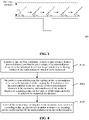
- FIG. 1 is a first flowchart of a method for measuring dimension of a semiconductor structure according to an embodiment of the present disclosure.
- An execution body of the embodiment is an AFM or an external device connected with the AFM, or may be executed by the AFM and the external device connected with the AFM together.
- the method for measuring dimension of a semiconductor structure includes the following operations.
- a probe of the AFM is controlled to move a first distance from a preset reference position to a top surface of a semiconductor structure to be measured in a direction perpendicular to the top surface of the semiconductor structure to be measured.
- FIG. 2 is a first schematic diagram of a scenario in which the dimension of a semiconductor structure is measured according to an embodiment of the present disclosure.
- the probe 200 of the AFM may be controlled to move the first distance Z 1 from the preset reference position to the top surface 101 of the semiconductor structure 100 to be measured in the direction perpendicular to the top surface 101 of the semiconductor structure 100 to be measured.
- a vertical distance between the reference position and the top surface 101 of the semiconductor structure 100 is greater than the first distance Z ⁇ 1 .
- the probe is controlled to scan the surface of the semiconductor structure to be measured while keeping the first distance in a direction parallel to the top surface of the semiconductor structure to be measured, and amplitudes of the probe at respective scanning points on the surface of the semiconductor structure to be measured are detected.
- FIG. 3 is a second schematic diagram of a scenario in which the dimension of a semiconductor structure is measured according to an embodiment of the present disclosure.
- the probe 200 is controlled to scan the surface 101 of the semiconductor structure 100 to be measured keeping the first distance Z ⁇ 1 in the direction parallel to the top surface 101 of the semiconductor structure 100 to be measured. For example, scanning is performed sequentially at scanning point A2, scanning point A3, scanning point A4, scanning point A5, etc., from scanning point A1.
- a distance between the probe 200 and the reference position keeps the first distance Z ⁇ 1 in a scanning process. That is, when there is a trench in the top surface 101 of the semiconductor structure 100 to be measured, the probe may not descend into the trench for scanning, and instead, keeps the first distance Z ⁇ 1 from the reference position for scanning.
- a driving frequency of the probe 200 is kept unchanged. That is, the amplitude of the probe 200 is kept unchanged when there is no acting force or an acting force on the probe is kept unchanged.
- the amplitudes of the probe 200 at each scanning point are detected in real time.
- a CD of the semiconductor structure to be measured is determined according to the amplitudes of the probe at respective scanning points on the surface of the semiconductor structure to be measured.
- an interaction force of the surface of the semiconductor structure on the probe may be stronger.
- the driving frequency of the probe is kept unchanged, the interaction force on the probe is stronger, and the amplitude of the probe may be lower.
- a changing condition of the distance between the probe of the AFM and the surface of the semiconductor structure to be measured may be determined according to a changing condition of the amplitudes of the probe at respective scanning points on the surface of the semiconductor structure to be measured, thereby determining the CD of the semiconductor structure to be measured.
- the semiconductor structure to be measured is a photoresistor.
- CD-SEM Critical Dimension-Scanning Electron Microscope
- the CD-SEM mainly implements measurement based on electron-beam bombardment over a surface of the semiconductor, and since surface strength of a photoresistor is relatively low, the existing CD-SEM cannot measure a CD of the photoresistor accurately.
- a measurement manner of the AFM is improved, so that the AFM may be applied to CD measurement of a photoresistor with a high-aspect-ratio trench, and is wider in application range.
- a spacing distance between the probe of the AFM and the surface of the semiconductor structure to be measured is not affected by a surface structure of the semiconductor structure to be measured, so that, when there is a trench with a small width but a relatively great depth-to-width ratio, i.e., a trench with a high aspect ratio, in the surface of the semiconductor structure to be measured, the probe may not descend into the trench for scanning and contact with a sidewall of the trench in the measurement process, which avoids damages to the semiconductor structure to be measured.
- the amplitudes of the probe at respective scanning points on the surface of the semiconductor structure to be measured are detected to determine the CD of the semiconductor structure to be measured, and an interaction force between the semiconductor structure to be measured and the probe is not required to be detected, so that a measurement manner is simple, influences of the surface structure of the semiconductor structure to be measured are eliminated, and the present disclosure range is wider.
- FIG. 4 is a second flowchart of a method for measuring dimension of a semiconductor structure according to an embodiment of the present disclosure.
- the method for measuring dimension of a semiconductor structure further includes the following operations.
- the probe is controlled to move the first distance from the preset reference position to a top surface of a semiconductor reference sample in a direction perpendicular to the top surface of the semiconductor reference sample.
- the reference position may be preset.
- the probe of the AFM When the semiconductor reference sample is fixed on a measurement table of the AFM, and the probe of the AFM is at the reference position, the probe of the AFM may be free of an acting force of the top surface of the semiconductor reference sample.
- the semiconductor reference sample can be understood as a semiconductor structure with the same surface structure as the semiconductor structure to be measured.
- the first distance may be determined at first through the following operations.
- a first amplitude when the probe is at the preset reference position and a driving frequency is a target driving frequency value and a second amplitude when the probe moves the first distance in the direction perpendicular to the top surface of the semiconductor reference sample and the driving frequency is the target driving frequency value are determined according to relation between a curve of an amplitude and driving frequency of the probe in absence of an acting force and a curve of an amplitude and driving frequency of the probe in presence of an acting force.
- FIG. 5 is a schematic diagram of the relation between a curve of n amplitude and driving frequency of a probe of an AFM in the absence of an acting force and a curve of n amplitude and driving frequency of a probe of an AFM in the presence of an acting force according to an embodiment of the present disclosure.
- the amplitude of the probe of the AFM may change with the driving frequency in the absence and presence of the acting force.
- a maximum value of a difference ⁇ A between amplitudes of the probe of the AFM in the absence and presence of the acting force may be determined, namely a "maximum slope position" shown in FIG. 5 may be determined, according to the diagram of the curvilinear relations between the amplitude and driving frequency of the probe of the AFM in the absence and presence of the acting force.
- a driving frequency corresponding to the "maximum slope position" is determined as the target driving frequency value.
- the driving frequency is the target driving frequency value
- the amplitude of the probe of the AFM in the absence of the acting force is determined as the first amplitude
- the amplitude of the probe of the AFM in the presence of the acting force is determined as the second amplitude.
- step b the probe is adjusted to the preset reference position, and the driving frequency of the probe is adjusted to the target driving frequency value.
- step c the probe is controlled to move for multiple times from the preset reference position in the direction perpendicular to the top surface of the semiconductor reference sample, and movement distances that the probe moves every time and amplitudes of the probe after respective movements are recorded until the amplitude of the probe is the second amplitude, all the amplitudes of the probe after respective movements being more than or equal to the second amplitude.
- the probe may be controlled to move the distance Z ⁇ i from the preset reference position in the direction perpendicular to the top surface of the semiconductor reference sample, and an amplitude of the probe after movement is recorded. Then, the probe is controlled to move the distance Z ⁇ i from the preset reference position in the direction perpendicular to the top surface of the semiconductor reference sample, and an amplitude of the probe after movement is recorded. Such operations are repeated until the amplitude of the probe is the second amplitude.
- distance Z i first distance/n.
- a magnitude of n may be preset. For example, n ⁇ 30 is set.
- the probe may be controlled to move a random distance from the preset reference position in the direction perpendicular to the top surface of the semiconductor reference sample, and an amplitude of the probe after movement is recorded. Then, the probe is controlled to move a random distance from the preset reference position in the direction perpendicular to the top surface of the semiconductor reference sample, and an amplitude of the probe after movement is recorded. Such operations are repeated until the amplitude of the probe is the second amplitude.
- step d the first distance is determined according to the recorded movement distances that the probe moves every time.
- preset prompting information is output for prompting a tester that the surface of the semiconductor structure to be measured is abnormal.
- the probe is controlled to scan the top surface of the semiconductor reference sample while keeping the first distance in a direction parallel to the top surface of the semiconductor reference sample, and amplitudes of the probe at respective scanning points on the top surface of the semiconductor reference sample are detected.
- a first amplitude threshold and a second amplitude threshold are determined according to the amplitudes of the probe at respective scanning points on the top surface of the semiconductor reference sample.
- the operation, described in S103, that the CD of the semiconductor structure to be measured is determined according to the amplitudes of the probe at respective scanning points on the surface of the semiconductor structure to be measured specifically includes the following operations.
- a first identifier is output at the present scanning point. For example, if the amplitude at the present scanning point on the surface of the semiconductor structure to be measured is greater than or equal to the first amplitude threshold and less than or equal to the second amplitude threshold, "1" is output at the present scanning point. If the amplitude at the present scanning point on the surface of the semiconductor structure to be measured is greater than the second amplitude threshold, a second identifier is output at the present scanning point. For example, if the amplitude at the present scanning point on the surface of the semiconductor structure to be measured is greater than the second amplitude threshold, "0" is output at the present scanning point.
- the acting force of the top surface of the semiconductor reference sample on the probe may substantially be kept in a relatively small range, namely the amplitudes of the probe at respective scanning points on the top surface of the semiconductor reference sample may be in a relatively small range.
- the amplitude at the present scanning point on the surface of the semiconductor structure to be measured is greater than the first amplitude threshold and less than the second amplitude threshold, it indicates that a distance between the present scanning point and the probe is in a normal range; and when the amplitude at the present scanning point on the surface of the semiconductor structure to be measured is greater than or equal to the second amplitude threshold, it indicates that the distance between the present scanning point and the probe clearly increases, and it can be inferred that the present scanning point is above a trench in the surface of the semiconductor structure to be measured.
- the preset prompting information is output for prompting the tester that the surface of the semiconductor structure to be measured is abnormal.
- the amplitude at the present scanning point on the surface of the semiconductor structure to be measured is less than or equal to the first amplitude threshold, it indicates that the distance between the present scanning point and the probe clearly decreases, and it can be inferred that the present scanning point may be abnormal, for example, there may be a particle, a process residue, a bump, etc., at the present scanning point.
- the prompting information may be output to prompt the tester that the surface of the semiconductor structure to be measured is abnormal and bring conveniences to specialized analysis of the tester.
- FIG. 6 is a third flowchart of a method for measuring dimension of a semiconductor structure according to an embodiment of the present disclosure.
- the method for measuring dimension of a semiconductor structure includes the following operations.
- a probe is controlled to move a distance Z ⁇ 1 from a preset reference position to a top surface of a semiconductor structure to be measured.
- the probe is controlled to scan the surface of the semiconductor structure to be measured keeping the distance Z ⁇ 1 in a direction parallel to the top surface of the semiconductor structure to be measured, and amplitudes of the probe at respective scanning points on the surface of the semiconductor structure to be measured are detected.
- a CD of the semiconductor structure to be measured is determined according to output identifiers.
- a first region where the first identifier "1" output when the surface of the semiconductor structure to be measured is scanned is distributed and a second region where the output second identifier "0" is distributed may be determined at first. Then, a boundary between the first region and the second region is determined, and the CD of the semiconductor structure to be measured is determined according to the boundary between the first region and the second region.
- FIG. 7 is a schematic diagram of distribution regions of first identifiers and second identifiers output when a top surface of a semiconductor structure to be measured is scanned according to an embodiment of the present disclosure.
- an embodiment of the present disclosure also provides a CD measurement apparatus.
- the CD measurement apparatus 80 includes a control module 801, a detection module 802, and a processing module 803.
- the control module 801 is configured to control a probe of an AFM to move a first distance from a preset reference position to a top surface of a semiconductor structure to be measured in a direction perpendicular to the top surface of the semiconductor structure to be measured.
- the detection module 802 is configured to control the probe to scan the surface of the semiconductor structure to be measured while keeping the first distance in a direction parallel to the top surface of the semiconductor structure to be measured, and detect amplitudes of the probe at respective scanning points on the surface of the semiconductor structure to be measured.
- the processing module 803 is configured to determine a CD of the semiconductor structure to be measured according to the amplitudes of the probe at respective scanning points on the surface of the semiconductor structure to be measured.
- a spacing distance between the probe of the AFM and the top surface of the semiconductor structure to be measured is not affected by a surface structure of the semiconductor structure to be measured, so that, when there is a trench with a small width but a relatively great depth-to-width ratio, i.e., a trench with a high aspect ratio, in the surface of the semiconductor structure to be measured, the probe may not descend into the trench for scanning and contact with a sidewall of the trench in the measurement process, which avoids damages to the semiconductor structure to be measured.
- the amplitudes of the probe at respective scanning points on the surface of the semiconductor structure to be measured are detected to determine the CD of the semiconductor structure to be measured, and an interaction force between the semiconductor structure to be measured and the probe is not required to be detected, so that a measurement manner is simple, influences of the surface structure of the semiconductor structure to be measured are eliminated, and the present disclosure range is wider.
- control module 801 is further configured to control the probe to move the first distance from the preset reference position to a top surface of a semiconductor reference sample in a direction perpendicular to the top surface of the semiconductor reference sample.
- the detection module 802 is further configured to control the probe to scan the top surface of the semiconductor reference sample while keeping the first distance in a direction parallel to the top surface of the semiconductor reference sample, and detect amplitudes of the probe at respective scanning points on the top surface of the semiconductor reference sample.
- the processing module 803 is further configured to determine a first amplitude threshold and a second amplitude threshold according to the amplitudes of the probe at respective scanning points on the top surface of the semiconductor reference sample.
- processing module 803 is specifically configured to:
- processing module 803 is specifically configured to:
- processing module 803 is specifically configured to:
- the CD measurement apparatus 80 further includes a prompting module.
- the prompting module is configured to, if the amplitude at the present scanning point on the surface of the semiconductor structure to be measured is less than the first amplitude threshold, output preset prompting information for prompting a tester that the surface of the semiconductor structure to be measured is abnormal.
- control module 801 is further configured to:
- the processing module 803 is further configured to: determine the first distance according to the recorded movement distances that the probe moves every time.
- contents specifically executed by the control module 801, detection module 802, and processing module 803 in the embodiment of the present disclosure may refer to the related contents in the embodiments shown in FIG. 1 to FIG. 7 , and will not be elaborated herein.
- an embodiment of the present disclosure also provides an AFM, which includes at least one processor and a memory.
- the memory stores a computer-executable instruction.
- the at least one processor executes the computer-executable instruction stored in the memory to implement each step in the method for measuring dimension of a semiconductor structure described in the abovementioned embodiment. Elaborations are omitted in the embodiment.
- FIG. 9 is a hardware structure diagram of an AFM according to an embodiment of the present disclosure.
- the AFM 90 of the embodiment includes a processor 901 and a memory 902.
- the memory 902 is configured to store a computer-executable instruction.
- the processor 901 is configured to execute the computer-executable instruction stored in the memory to implement each step of the method for measuring dimension of a semiconductor structure described in the abovementioned embodiments, specifically referring to the related descriptions in the method embodiments. Elaborations are omitted in the embodiment.
- the memory 902 may be independent, or may be integrated with the processor 901.
- the device further includes a bus 903, configured to connect the memory 902 with the processor 901.
- an embodiment of the present disclosure also provides a computer-readable storage medium, in which a computer-executable instruction is stored.
- the computer-executable instruction is executed by a processor to implement each step in the method for measuring dimension of a semiconductor structure described in the abovementioned embodiments, specifically referring to the related descriptions in the method embodiments. Elaborations are omitted in the embodiment.
- an embodiment of the present disclosure also provides a computer program product, which includes a computer program.
- the computer program is executed by a processor to implement each step in the method for measuring dimension of a semiconductor structure described in the abovementioned embodiments, specifically referring to the related descriptions in the method embodiments. Elaborations are omitted in the embodiment.
- the disclosed device and method may be implemented in another manner.
- the device embodiment described above is only schematic, and for example, division of the modules is only logic function division, and other division manners may be adopted during practical implementation.
- multiple modules may be combined or integrated into another system, or some characteristics may be neglected or not executed.
- coupling or direct coupling or communication connection between each displayed or discussed component may be indirect coupling or communication connection, implemented through some interfaces, of the apparatus or the modules, and may be electrical and mechanical or adopt other forms.
- modules described as separate parts may or may not be physically separated, and parts displayed as modules may or may not be physical units, and namely may be located in the same place, or may also be distributed to multiple network units. Part or all of the modules may be selected to achieve the purposes of the solutions of the embodiments as practically required.
- each function module in each embodiment of the present disclosure may be integrated into a processing module, or each module may also physically exist independently, or two or more than two modules may also be integrated into a module.
- the integrated module may be implemented in a hardware form, or may be implemented in form of hardware and software function unit.
- the integrated module implemented in form of a software function module may be stored in a computer-readable storage medium.
- the software function module is stored in a storage medium, including a plurality of instructions configured to enable a computer device (which may be a personal computer, a server, a network device, etc.) or a processor to execute part of the steps of the method in each embodiment of the present disclosure.
- the processor may be a Central Processing Unit (CPU), or may be another general-purpose processor, a Digital Signal Processor (DSP), an Application Specific Integrated Circuit (ASIC), etc.
- the general-purpose processor may be a microprocessor, or the processor may also be any conventional processor, etc.
- the steps of the method disclosed in combination with the present disclosure may be directly embodied to be executed and completed by a hardware processor or executed and completed by a combination of hardware and software modules in the processor.
- the memory may include a high-speed Random Access Memory (RAM), or may include a Non-Volatile Memory (NVM), for example, at least one disk memory, or may be a U disk, a mobile hard disk, a Read-Only Memory (ROM), a magnetic disk, an optical disk, etc.
- RAM Random Access Memory
- NVM Non-Volatile Memory
- the bus may be an Industry Standard Architecture (ISA) bus, a Peripheral Component Interconnect (PCI) bus, an Extended Industry Standard Component (EISA) bus, etc.
- ISA Industry Standard Architecture
- PCI Peripheral Component Interconnect
- EISA Extended Industry Standard Component
- the bus may be divided into an address bus, a data bus, a control bus, etc.
- the bus in the drawings of the present disclosure is not limited to one bus or one type of bus.
- the storage medium may be implemented by a volatile or non-volatile storage device of any type or a combination thereof, for example, a Static Random Access Memory (SRAM), an Electrically Erasable Programmable Read-Only Memory (EEPROM), an Erasable Programmable Read-Only Memory (EPROM), a Programmable Read-Only Memory (PROM), a ROM, a magnetic memory, a flash memory, a magnetic disk or an optical disk.
- SRAM Static Random Access Memory
- EEPROM Electrically Erasable Programmable Read-Only Memory
- EPROM Erasable Programmable Read-Only Memory
- PROM Programmable Read-Only Memory
- ROM Read-Only Memory
- the storage medium may be any available medium accessible for a universal or dedicated computer.
- An exemplary storage medium is coupled to the processor, thereby enabling the processor to read information from the storage medium and write information into the storage medium.
- the storage medium may also be a component of the processor.
- the processor and the storage medium may be in an ASIC.
- the processor and the storage medium may also exist in an electronic device or a master control device as discrete components.
- the program may be stored in a computer-readable storage medium.
- the program is executed to execute the steps of each method embodiment.
- the storage medium includes various media capable of storing program codes such as a ROM, a RAM, a magnetic disk or an optical disk.
Landscapes
- Physics & Mathematics (AREA)
- Health & Medical Sciences (AREA)
- General Health & Medical Sciences (AREA)
- General Physics & Mathematics (AREA)
- Nuclear Medicine, Radiotherapy & Molecular Imaging (AREA)
- Radiology & Medical Imaging (AREA)
- Testing Or Measuring Of Semiconductors Or The Like (AREA)
Applications Claiming Priority (2)
| Application Number | Priority Date | Filing Date | Title |
|---|---|---|---|
| CN202110053191.8A CN114765113B (zh) | 2021-01-15 | 2021-01-15 | 半导体结构尺寸的测量方法及设备 |
| PCT/CN2021/098842 WO2022151645A1 (zh) | 2021-01-15 | 2021-06-08 | 半导体结构尺寸的测量方法及设备 |
Publications (3)
| Publication Number | Publication Date |
|---|---|
| EP4050643A1 true EP4050643A1 (de) | 2022-08-31 |
| EP4050643A4 EP4050643A4 (de) | 2024-05-15 |
| EP4050643B1 EP4050643B1 (de) | 2025-08-06 |
Family
ID=82406158
Family Applications (1)
| Application Number | Title | Priority Date | Filing Date |
|---|---|---|---|
| EP21772656.1A Active EP4050643B1 (de) | 2021-01-15 | 2021-06-08 | Verfahren und vorrichtung zur messung der dimension einer halbleiterstruktur |
Country Status (2)
| Country | Link |
|---|---|
| US (1) | US11656245B2 (de) |
| EP (1) | EP4050643B1 (de) |
Family Cites Families (5)
| Publication number | Priority date | Publication date | Assignee | Title |
|---|---|---|---|---|
| JP3290586B2 (ja) * | 1996-03-13 | 2002-06-10 | セイコーインスツルメンツ株式会社 | 走査型近視野光学顕微鏡 |
| US6715346B2 (en) * | 2002-08-13 | 2004-04-06 | Infineon Technologies Ag | Atomic force microscopy scanning methods |
| CN1727871A (zh) | 2004-01-14 | 2006-02-01 | Fei公司 | 探针显微镜的操作方法 |
| US7202691B2 (en) * | 2005-05-31 | 2007-04-10 | Semiconductor Diagnostics, Inc. | Non-contact method for acquiring charge-voltage data on miniature test areas of semiconductor product wafers |
| DE102016214658B4 (de) | 2016-08-08 | 2020-10-08 | Carl Zeiss Smt Gmbh | Rastersondenmikroskop und Verfahren zum Untersuchen einer Probenoberfläche |
-
2021
- 2021-06-08 EP EP21772656.1A patent/EP4050643B1/de active Active
- 2021-08-03 US US17/392,430 patent/US11656245B2/en active Active
Also Published As
| Publication number | Publication date |
|---|---|
| EP4050643A4 (de) | 2024-05-15 |
| EP4050643B1 (de) | 2025-08-06 |
| US11656245B2 (en) | 2023-05-23 |
| US20220229087A1 (en) | 2022-07-21 |
Similar Documents
| Publication | Publication Date | Title |
|---|---|---|
| TWI719119B (zh) | 掃描型探針顯微鏡及其探針接觸檢測方法 | |
| US11131709B2 (en) | Probe systems for optically probing a device under test and methods of operating the probe systems | |
| WO2021067049A1 (en) | Probe systems for optically probing a device under test and methods of operating the probe systems | |
| US20190064014A1 (en) | Interface ultrasonic reflectivity-pressure relation curve establishment method and loading testbed | |
| CN114200362A (zh) | 基于nv色心的芯片磁场检测方法及装置 | |
| CN114765113B (zh) | 半导体结构尺寸的测量方法及设备 | |
| US6545273B1 (en) | Use of multiple tips on AFM to deconvolve tip effects | |
| EP4050643B1 (de) | Verfahren und vorrichtung zur messung der dimension einer halbleiterstruktur | |
| US12203959B2 (en) | Methods of establishing contact between a probe tip of a probe system and a device under test, probe systems that perform the methods, and storage media that directs probe systems to perform the methods | |
| CN119008448A (zh) | 边缘不完整区域wat测试方法、系统及可读存储介质 | |
| US6961670B2 (en) | Probe testing method and apparatus for determining acceptable/defective end shape of contact probe through image analysis | |
| CN116203292A (zh) | 一种测试方法、设备及机台 | |
| US6545470B2 (en) | Scanning probe microscope | |
| US7617720B2 (en) | Surface position measuring method and surface position measuring device | |
| JP2002062123A (ja) | 荷電ビーム測長装置及び測長方法 | |
| JP3227434U (ja) | 電子部品ハンドリング装置及び電子部品試験装置 | |
| CN119068957B (zh) | 芯片测试方法及电路 | |
| JP7808303B1 (ja) | 状態判定装置、方法、プログラム、記録媒体 | |
| US5122739A (en) | STM-like device and method for measuring node voltages on integrated circuits | |
| JP7521830B2 (ja) | 接触又は接続状態の判定方法及び情報処理装置 | |
| CN121510933A (zh) | 晶圆的金属水平检测方法、装置、设备及计算机存储介质 | |
| EP0485202B1 (de) | Anwendung eines STM-artigen Systems zur Messung der Knotenspannung in integrierten Schaltungen | |
| WO2004085959A1 (ja) | 試料観察装置、エッジ位置算出装置、及びプログラム | |
| JP2009164538A (ja) | 閾値電圧演算方法、閾値電圧演算プログラムおよび閾値電圧演算装置 | |
| JP3298473B2 (ja) | 探針形状適合判定及び表面形状の測定方法 |
Legal Events
| Date | Code | Title | Description |
|---|---|---|---|
| STAA | Information on the status of an ep patent application or granted ep patent |
Free format text: STATUS: UNKNOWN |
|
| STAA | Information on the status of an ep patent application or granted ep patent |
Free format text: STATUS: THE INTERNATIONAL PUBLICATION HAS BEEN MADE |
|
| PUAI | Public reference made under article 153(3) epc to a published international application that has entered the european phase |
Free format text: ORIGINAL CODE: 0009012 |
|
| STAA | Information on the status of an ep patent application or granted ep patent |
Free format text: STATUS: REQUEST FOR EXAMINATION WAS MADE |
|
| 17P | Request for examination filed |
Effective date: 20210927 |
|
| AK | Designated contracting states |
Kind code of ref document: A1 Designated state(s): AL AT BE BG CH CY CZ DE DK EE ES FI FR GB GR HR HU IE IS IT LI LT LU LV MC MK MT NL NO PL PT RO RS SE SI SK SM TR |
|
| REG | Reference to a national code |
Ref country code: DE Ref legal event code: R079 Free format text: PREVIOUS MAIN CLASS: H01L0021660000 Ipc: G01Q0010060000 Ref document number: 602021035691 Country of ref document: DE |
|
| DAV | Request for validation of the european patent (deleted) | ||
| DAX | Request for extension of the european patent (deleted) | ||
| A4 | Supplementary search report drawn up and despatched |
Effective date: 20240411 |
|
| RIC1 | Information provided on ipc code assigned before grant |
Ipc: H01L 21/66 20060101ALI20240405BHEP Ipc: G01Q 30/04 20100101ALI20240405BHEP Ipc: G01Q 10/06 20100101AFI20240405BHEP |
|
| STAA | Information on the status of an ep patent application or granted ep patent |
Free format text: STATUS: EXAMINATION IS IN PROGRESS |
|
| 17Q | First examination report despatched |
Effective date: 20241210 |
|
| GRAP | Despatch of communication of intention to grant a patent |
Free format text: ORIGINAL CODE: EPIDOSNIGR1 |
|
| STAA | Information on the status of an ep patent application or granted ep patent |
Free format text: STATUS: GRANT OF PATENT IS INTENDED |
|
| INTG | Intention to grant announced |
Effective date: 20250411 |
|
| GRAS | Grant fee paid |
Free format text: ORIGINAL CODE: EPIDOSNIGR3 |
|
| P01 | Opt-out of the competence of the unified patent court (upc) registered |
Free format text: CASE NUMBER: APP_25353/2025 Effective date: 20250528 |
|
| GRAA | (expected) grant |
Free format text: ORIGINAL CODE: 0009210 |
|
| STAA | Information on the status of an ep patent application or granted ep patent |
Free format text: STATUS: THE PATENT HAS BEEN GRANTED |
|
| AK | Designated contracting states |
Kind code of ref document: B1 Designated state(s): AL AT BE BG CH CY CZ DE DK EE ES FI FR GB GR HR HU IE IS IT LI LT LU LV MC MK MT NL NO PL PT RO RS SE SI SK SM TR |
|
| REG | Reference to a national code |
Ref country code: GB Ref legal event code: FG4D |
|
| REG | Reference to a national code |
Ref country code: CH Ref legal event code: EP |
|
| REG | Reference to a national code |
Ref country code: IE Ref legal event code: FG4D |
|
| REG | Reference to a national code |
Ref country code: DE Ref legal event code: R096 Ref document number: 602021035691 Country of ref document: DE |
|
| REG | Reference to a national code |
Ref country code: NL Ref legal event code: MP Effective date: 20250806 |
|
| PG25 | Lapsed in a contracting state [announced via postgrant information from national office to epo] |
Ref country code: IS Free format text: LAPSE BECAUSE OF FAILURE TO SUBMIT A TRANSLATION OF THE DESCRIPTION OR TO PAY THE FEE WITHIN THE PRESCRIBED TIME-LIMIT Effective date: 20251206 |
|
| PG25 | Lapsed in a contracting state [announced via postgrant information from national office to epo] |
Ref country code: NO Free format text: LAPSE BECAUSE OF FAILURE TO SUBMIT A TRANSLATION OF THE DESCRIPTION OR TO PAY THE FEE WITHIN THE PRESCRIBED TIME-LIMIT Effective date: 20251106 |
|
| REG | Reference to a national code |
Ref country code: LT Ref legal event code: MG9D |
|
| PG25 | Lapsed in a contracting state [announced via postgrant information from national office to epo] |
Ref country code: PT Free format text: LAPSE BECAUSE OF FAILURE TO SUBMIT A TRANSLATION OF THE DESCRIPTION OR TO PAY THE FEE WITHIN THE PRESCRIBED TIME-LIMIT Effective date: 20251209 |
|
| PG25 | Lapsed in a contracting state [announced via postgrant information from national office to epo] |
Ref country code: FI Free format text: LAPSE BECAUSE OF FAILURE TO SUBMIT A TRANSLATION OF THE DESCRIPTION OR TO PAY THE FEE WITHIN THE PRESCRIBED TIME-LIMIT Effective date: 20250806 |
|
| PG25 | Lapsed in a contracting state [announced via postgrant information from national office to epo] |
Ref country code: HR Free format text: LAPSE BECAUSE OF FAILURE TO SUBMIT A TRANSLATION OF THE DESCRIPTION OR TO PAY THE FEE WITHIN THE PRESCRIBED TIME-LIMIT Effective date: 20250806 Ref country code: NL Free format text: LAPSE BECAUSE OF FAILURE TO SUBMIT A TRANSLATION OF THE DESCRIPTION OR TO PAY THE FEE WITHIN THE PRESCRIBED TIME-LIMIT Effective date: 20250806 |
|
| PG25 | Lapsed in a contracting state [announced via postgrant information from national office to epo] |
Ref country code: GR Free format text: LAPSE BECAUSE OF FAILURE TO SUBMIT A TRANSLATION OF THE DESCRIPTION OR TO PAY THE FEE WITHIN THE PRESCRIBED TIME-LIMIT Effective date: 20251107 |
|
| PG25 | Lapsed in a contracting state [announced via postgrant information from national office to epo] |
Ref country code: SE Free format text: LAPSE BECAUSE OF FAILURE TO SUBMIT A TRANSLATION OF THE DESCRIPTION OR TO PAY THE FEE WITHIN THE PRESCRIBED TIME-LIMIT Effective date: 20250806 |
|
| PG25 | Lapsed in a contracting state [announced via postgrant information from national office to epo] |
Ref country code: LV Free format text: LAPSE BECAUSE OF FAILURE TO SUBMIT A TRANSLATION OF THE DESCRIPTION OR TO PAY THE FEE WITHIN THE PRESCRIBED TIME-LIMIT Effective date: 20250806 |
|
| PG25 | Lapsed in a contracting state [announced via postgrant information from national office to epo] |
Ref country code: BG Free format text: LAPSE BECAUSE OF FAILURE TO SUBMIT A TRANSLATION OF THE DESCRIPTION OR TO PAY THE FEE WITHIN THE PRESCRIBED TIME-LIMIT Effective date: 20250806 Ref country code: PL Free format text: LAPSE BECAUSE OF FAILURE TO SUBMIT A TRANSLATION OF THE DESCRIPTION OR TO PAY THE FEE WITHIN THE PRESCRIBED TIME-LIMIT Effective date: 20250806 |
|
| PG25 | Lapsed in a contracting state [announced via postgrant information from national office to epo] |
Ref country code: RS Free format text: LAPSE BECAUSE OF FAILURE TO SUBMIT A TRANSLATION OF THE DESCRIPTION OR TO PAY THE FEE WITHIN THE PRESCRIBED TIME-LIMIT Effective date: 20251106 |
|
| PG25 | Lapsed in a contracting state [announced via postgrant information from national office to epo] |
Ref country code: ES Free format text: LAPSE BECAUSE OF FAILURE TO SUBMIT A TRANSLATION OF THE DESCRIPTION OR TO PAY THE FEE WITHIN THE PRESCRIBED TIME-LIMIT Effective date: 20250806 |
|
| REG | Reference to a national code |
Ref country code: AT Ref legal event code: MK05 Ref document number: 1822429 Country of ref document: AT Kind code of ref document: T Effective date: 20250806 |
|
| PG25 | Lapsed in a contracting state [announced via postgrant information from national office to epo] |
Ref country code: SM Free format text: LAPSE BECAUSE OF FAILURE TO SUBMIT A TRANSLATION OF THE DESCRIPTION OR TO PAY THE FEE WITHIN THE PRESCRIBED TIME-LIMIT Effective date: 20250806 |
|
| PG25 | Lapsed in a contracting state [announced via postgrant information from national office to epo] |
Ref country code: DK Free format text: LAPSE BECAUSE OF FAILURE TO SUBMIT A TRANSLATION OF THE DESCRIPTION OR TO PAY THE FEE WITHIN THE PRESCRIBED TIME-LIMIT Effective date: 20250806 |
|
| PG25 | Lapsed in a contracting state [announced via postgrant information from national office to epo] |
Ref country code: AT Free format text: LAPSE BECAUSE OF FAILURE TO SUBMIT A TRANSLATION OF THE DESCRIPTION OR TO PAY THE FEE WITHIN THE PRESCRIBED TIME-LIMIT Effective date: 20250806 |
|
| PG25 | Lapsed in a contracting state [announced via postgrant information from national office to epo] |
Ref country code: IT Free format text: LAPSE BECAUSE OF FAILURE TO SUBMIT A TRANSLATION OF THE DESCRIPTION OR TO PAY THE FEE WITHIN THE PRESCRIBED TIME-LIMIT Effective date: 20250806 |
|
| PG25 | Lapsed in a contracting state [announced via postgrant information from national office to epo] |
Ref country code: CZ Free format text: LAPSE BECAUSE OF FAILURE TO SUBMIT A TRANSLATION OF THE DESCRIPTION OR TO PAY THE FEE WITHIN THE PRESCRIBED TIME-LIMIT Effective date: 20250806 |
|
| PG25 | Lapsed in a contracting state [announced via postgrant information from national office to epo] |
Ref country code: SK Free format text: LAPSE BECAUSE OF FAILURE TO SUBMIT A TRANSLATION OF THE DESCRIPTION OR TO PAY THE FEE WITHIN THE PRESCRIBED TIME-LIMIT Effective date: 20250806 Ref country code: EE Free format text: LAPSE BECAUSE OF FAILURE TO SUBMIT A TRANSLATION OF THE DESCRIPTION OR TO PAY THE FEE WITHIN THE PRESCRIBED TIME-LIMIT Effective date: 20250806 |