EP4048201B1 - Retinale prothesen - Google Patents
Retinale prothesen Download PDFInfo
- Publication number
- EP4048201B1 EP4048201B1 EP20879132.7A EP20879132A EP4048201B1 EP 4048201 B1 EP4048201 B1 EP 4048201B1 EP 20879132 A EP20879132 A EP 20879132A EP 4048201 B1 EP4048201 B1 EP 4048201B1
- Authority
- EP
- European Patent Office
- Prior art keywords
- jfet
- pixel
- retinal
- photo
- retinal prosthesis
- Prior art date
- Legal status (The legal status is an assumption and is not a legal conclusion. Google has not performed a legal analysis and makes no representation as to the accuracy of the status listed.)
- Active
Links
Images




Classifications
-
- A—HUMAN NECESSITIES
- A61—MEDICAL OR VETERINARY SCIENCE; HYGIENE
- A61N—ELECTROTHERAPY; MAGNETOTHERAPY; RADIATION THERAPY; ULTRASOUND THERAPY
- A61N1/00—Electrotherapy; Circuits therefor
- A61N1/02—Details
- A61N1/04—Electrodes
- A61N1/05—Electrodes for implantation or insertion into the body, e.g. heart electrode
- A61N1/0526—Head electrodes
- A61N1/0543—Retinal electrodes
-
- A—HUMAN NECESSITIES
- A61—MEDICAL OR VETERINARY SCIENCE; HYGIENE
- A61N—ELECTROTHERAPY; MAGNETOTHERAPY; RADIATION THERAPY; ULTRASOUND THERAPY
- A61N1/00—Electrotherapy; Circuits therefor
- A61N1/02—Details
- A61N1/08—Arrangements or circuits for monitoring, protecting, controlling or indicating
-
- A—HUMAN NECESSITIES
- A61—MEDICAL OR VETERINARY SCIENCE; HYGIENE
- A61N—ELECTROTHERAPY; MAGNETOTHERAPY; RADIATION THERAPY; ULTRASOUND THERAPY
- A61N1/00—Electrotherapy; Circuits therefor
- A61N1/18—Applying electric currents by contact electrodes
- A61N1/32—Applying electric currents by contact electrodes alternating or intermittent currents
- A61N1/36—Applying electric currents by contact electrodes alternating or intermittent currents for stimulation
- A61N1/36046—Applying electric currents by contact electrodes alternating or intermittent currents for stimulation of the eye
-
- H—ELECTRICITY
- H10—SEMICONDUCTOR DEVICES; ELECTRIC SOLID-STATE DEVICES NOT OTHERWISE PROVIDED FOR
- H10F—INORGANIC SEMICONDUCTOR DEVICES SENSITIVE TO INFRARED RADIATION, LIGHT, ELECTROMAGNETIC RADIATION OF SHORTER WAVELENGTH OR CORPUSCULAR RADIATION
- H10F39/00—Integrated devices, or assemblies of multiple devices, comprising at least one element covered by group H10F30/00, e.g. radiation detectors comprising photodiode arrays
- H10F39/10—Integrated devices
- H10F39/12—Image sensors
- H10F39/196—Junction field effect transistor [JFET] image sensors; Static induction transistor [SIT] image sensors
Definitions
- the present subject disclosure relates to retinal prostheses. More specifically, the present subject disclosure relates to retinal prostheses which include a single or array of photosensitive junction field-effect-transistors (Photo-JFET).
- Photo-JFET photosensitive junction field-effect-transistors
- Degenerative retinal diseases including Retinitis Pigmentosa (RP) and Age-Related Macular Degeneration (AMD), are leading causes of blindness worldwide. Globally, about 1.5 million people (possibly 1 in 4000) are affected by RP and 50 million or more individuals suffer from AMD [1-3].
- Patients with retinal degenerative diseases suffer from the selective loss of the photoreceptive cells of the retina, while the remaining retina remains intact.
- Retinal implants transduce visual information into current for neural stimulation with the goal of replacing lost photoreceptor function in patients blinded by degenerative diseases. These implants, known as retinal prostheses, aim to reestablish high acuity central vision with sufficiently large visual field without compromising any residual functional areas of the retina [4].
- a retinal prosthesis consists of a pixelated image sensor, a stimulation encoder, an array of neural stimulation electrodes, and a power supply.
- One category of retinal implant utilizes a head mounted camera to capture the visual scene that is relayed by a wireless inductive link to an implanted microprocessor.
- the microprocessor encodes the visual scene and relays necessary neural stimulation parameters to an array of directly wired stimulation electrodes implanted in close proximity to retinal neurons [5].
- a prominent example of such a retinal implant is the Argus II Retinal Prosthesis (Second Sight Medical Technologies) which has received FDA approval (2014) and CE Mark (2011) to treat Retinitis Pigmentosa patients with bare or no light perception. The best visual acuity result in Argus II patients is on the order of 20/1260 [6,7].
- Another category of retinal implant utilizes a directly implanted microphotodiode array (MPDA) to convert the spatiotemporal pattern of light impinging on the MPDA into electrical currents to stimulate the retina.
- MPDA microphotodiode array
- the intensity of light under typical natural retinal irradiance (0.001-1uW/mm 2 ) is orders of magnitude too low to be efficiently converted into electrical current for neural stimulation ( ⁇ A) by a single photodiode [8,9]. Therefore, one approach of MPDA implants is to utilize a CMOS amplifier circuit within each pixel to amplify the primary photocurrent.
- An advantage of the CMOS approach is that the implant can encode spatiotemporal contrast across any typical visual scene without the need for externally worn imaging components [10,11].
- the Alpha AMS/IMS system is an example of a MPDA CMOS retinal implant that has successfully received CE Mark. In clinical trials the Alpha AMS restored a best reported visual acuity nearing 20/546 [12,13].
- a drawback to the CMOS approach is the complexity of the required hardware that limits the fill factor and requires extensive encapsulation materials to electrically insulate the array and achieve biocompatibility [14].
- An alternative MPDA retinal prosthetic approach is to use photodiodes and an external light source in the NIR wavelength to power and control the current produced by the array. Pulsed near infrared light is used to optically address the implanted photodiodes with sufficient irradiance to produce photocurrent for neural stimulation.
- This solution can greatly simplify the form factor of the implanted hardware by using only photodiodes operated in photovoltaic mode or as actively biased pixels sharing a common power line [8,15-17].
- the prosthetic visual acuity of photodiode-only arrays is on the order of 20/200- 20/400 [18].
- the present disclosure presents a photosensitive junction field-effect-transistor (Photo-JFET) that integrates a photodetector, amplifier, and neural electrode stimulator within a single silicon pixel mesa, thus achieving gain without sacrificing fill factor.
- Photo-JFET photosensitive junction field-effect-transistor
- Incorporating a gain mechanism into the body of a photo sensing pixel further advances existing retinal prostheses by enabling scaling of pixel size down to 10-20 ⁇ m to achieve improved visual acuity over existing optoelectronic prostheses.
- a vertically integrated Photo-JFET pixel is provided that can produce a broad range of current (0.1-100 ⁇ A) for robust retinal neural stimulation within a safe range of NIR irradiance with the potential to restore high acuity vision for the smallest reported retinal prosthesis pixel size, with the potential to achieve a prosthetic visual acuity of around 20/60 within a safe range of NIR irradiance.
- the present subject disclosure is a retinal prosthesis.
- the retinal prosthesis includes a vertically integrated photosensitive junction field-effect-transistor (Photo-JFET); and a neural stimulating electrode.
- the present subject disclosure is a retinal prosthesis.
- the retinal prosthesis includes a vertically integrated photosensitive junction field-effect-transistor (Photo-JFET) having a silicon pixel mesa; and a neural stimulating electrode; wherein a current range of 0.1-100 ⁇ A is produced.
- Photo-JFET photosensitive junction field-effect-transistor
- the present subject disclosure is a retinal prosthesis.
- the retinal prosthesis includes a vertically integrated photosensitive junction field-effect-transistor (Photo-JFET) having a silicon pixel mesa and a pixel size range of 1-100 ⁇ m; and a neural stimulating electrode.
- Photo-JFET photosensitive junction field-effect-transistor
- the present subject disclosure addresses the shortcomings of conventional retinal prostheses by providing vertically integrated photo-JFET pixel architectures and methods of use.
- a vertically integrated Photo-JFET pixel may include a pair of back-to-back p/n diodes in parallel with a sidewall junction field-effect-transistor.
- the diodes can be configured in either a N-P-N or P-N-P configuration for a n-channel or p-channel JFET.
- a dielectric film is deposited on the sidewall of the silicon mesa to induce a weak inversion layer along the vertical edge of the middle layer of the back-to-back diode, forming a vertical channel along the mesa sidewall.
- Silicon dioxide (SiO 2 ) or aluminum oxide (Al 2 O 3 ), or other applicable material, may be used to control the pinch-off voltage of the sidewall JFET.
- a voltage bias applied across the top and bottom diodes can provide drain-source voltage (Vos) for the Photo-JFET, and the same voltage also provides reverse and forward bias of two back-to-back p/n junctions.
- the diode orientation can be reversed by changing the polarity of the source-drain bias.
- the Photo-JFET is normally off in the dark and can be turned on by incident light.
- the doping profile and thickness of the vertical N-P-N (or P-N-P) structure are designed in such a way that the structure does not perform as a regular bipolar transistor (i.e., the current gain of the bipolar structure h fe ⁇ 1) .
- the structure can be modeled as 2 back-to-back P/N diodes, and the only transistor function is provided by the sidewall JFET.
- FIG. 1A shows the design of a Photo-JFET pixel from a vertical etched mesa.
- a dielectric passivation layer deposited on the sidewall of the silicon mesa induces a channel along the vertical wall of the middle layer of the mesa.
- the sidewall view illustrates the pair of back-to-back p/n diodes and the junction field-effect-transistor (JFET) realized as an NPN or PNP stack.
- JFET junction field-effect-transistor
- FIG. 2B shows a scanning electron microscope micrograph (SEM) of a 13 ⁇ m Photo-JFET single pixel test structure.
- SEM scanning electron microscope micrograph
- FIG. 1C shows an SEM micrograph of prototype array with 40 ⁇ m pixels paired with 10 ⁇ m electrodes (light gray) spaced at 45 ⁇ m pitch, having a theoretical prosthetic acuity of 20/188.
- FIG. 1D shows an SEM micrograph of prototype array with 13 ⁇ m pixels paired with 10 ⁇ m electrodes (light gray) spaced at 15 ⁇ m pitch, having a theoretical acuity of 20/60.
- pixel sizes of 13 ⁇ m and 40 ⁇ m have been used throughout this disclosure as an example.
- the JFET architecture can be recognized in any size from 1-100 ⁇ m.
- groups of pixels can be operated as a single unit with a shared neural stimulating electrode. Such variations are within the scope of the present disclosure.
- V GS ⁇ V T ln 1 + I o 1 + I ph I o 2
- ⁇ the ideality factor
- V T the thermal voltage
- I o2 the reverse saturation current for the forward biased p/n junction. Note that in this design, V GS in Eqn. (1) is not only the voltage drop across the forward-biased p/n junction but also the gate-to-source voltage of the JFET.
- the threshold voltage required (V THmin ) to turn on the normally-off JFET will be greater than the V GS produced by dark current (I o1 ) but low enough such that the channel will turn on at low irradiance (Eqn. (2) for a N-channel JFET).
- a Photo-JFET can be engineered with high V TH and operated by optical addressing with NIR irradiance to control contrast and adjust the range of available photocurrent to the correct range for neural stimulation.
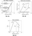
- Fig. 2A demonstrates the range of possible V GS calculated for lighting conditions spanning a range from retinal irradiance under dim lighting conditions to the typical irradiance of supplemental NIR light used in retinal prostheses as described above.
- V GS With sufficient illumination the V GS will exceed the threshold voltage (V TH ) to turn on the JFET and modulate the drain current (I D ) across the channel.
- the drain current in the saturation region for a normally-off N-channel JFET can be represented by Eqn. (3) where W is the effective channel width, equal to the circumference of the mesa, L is the length of the vertical channel, a is the effective channel width controlled by the thickness of charge inversion layer at the oxide-silicon mesa sidewall interface.
- the net output current in response to the input light is the sum of the original primary photocurrent across the back-to-back p/n junctions ( I ph ) and the drain current (I D ) through the sidewall JFET.
- I D W ⁇ ⁇ s 2 La V GS ⁇ V TH 2
- the total current produced by a Photo-JFET pixel under illumination is the sum of the drain current and the primary photocurrent (Eqn. (5)).
- the total current can be several orders of magnitude greater than the primary photocurrent produced by the photodiode layer.
- the dependence of the total current on the threshold voltage of a Photo-JFET calculated for a typical device dimension is shown in Fig. 2 .
- I Total I D + I ph + I o 1
- the total current produced in the dark condition is equivalent to the reverse saturation current, I o1 , of the reverse biased diode (Eqn. (6)).
- the actual reverse bias leakage current will likely be much higher than the theoretical value and will increase with the reverse bias voltage.
- the V TH of the Photo-JFET can be carefully engineered to achieve a photocurrent to dark current ratio between 10-10,000 depending upon the required intensity of irradiating light to turn on the JFET channel.
- I Total Dark I o 1
- FIG. 2 Shows a theoretical performance characteristics of a vertical silicon Photo-JFET using typical device parameters for a range of retinal irradiance.
- FIG. 2A shows calculated gate to source voltage (V GS ) for a range of irradiance conditions following Eqn. (1). Marked on the graph are the possible values of the threshold voltage to turn on the JFET channel for ideal case of minimum threshold, bright indoor retinal irradiance, and 200 ⁇ W/mm 2 supplemented NIR.
- FIG. 2B shows calculated total current (I Tot ) using the identified threshold voltages in FIG. 2A.
- FIG. 2C shows calculated gain achieved over the irradiance range. For simplicity, the subthreshold current in FIG. 2B-2C have been ignored, thus underestimating the total current and gain in subthreshold regime.
- the total current produced at the Photo-JFET pixel is delivered to retinal tissue through a stimulation electrode in contact with the top of the silicon mesa ( FIGS 1C-1D ).
- anodic stimulation current will be produced by applying positive bias to the top N layer and cathodic stimulation current will be produced by reversing the polarity of bias voltage.
- Each individual pixel in a retinal prosthesis implant must produce sufficient current to independently stimulate a region of retinal neural cells.
- the present subject disclosure is not limited to a single pixel but can be an array.
- the required output current per pixel to reach half-maximal effective stimulation with 10-30 ⁇ m diameter stimulation electrodes is reported to be between 1.8-7 ⁇ A based on in vitro studies [19].
- the stimulation threshold for individual cells within a single retina may vary due to differences in the morphology and phenotype, as well as the actual distance between stimulating electrodes and target cells over the entire span of an implanted array. Therefore, the total current produced by a Photo-JFET pixel must reach a level of ⁇ 10 ⁇ A for a safe range of NIR irradiance while the V TH of the JFET-channel must be sufficiently high such that the dark current will never inadvertently result in stimulation.
- a Photo-JFET device structure was realized by microfabrication techniques in a class 100 cleanroom facility.
- Single pixel test structures for device characterization ( FIG. 1B ) and array prototypes ( FIGS. 1C and 1D ) were formed by etching silicon mesas from an epitaxially grown wafer with doped sequential N-P-N layers on a N+ substrate.
- single pixel test structures were interfaced with neural stimulation electrodes fabricated on borosilicate glass discs. This transparent electrode substrate served as the bottom of the recording chamber to allow visualization of retinal neurons with differential interference microscopy for physiological recordings.
- Pixel mesas were fabricated at 13 ⁇ m and 40 ⁇ m diameter using a deep reactive ion etching and inductively coupled plasma process to a height of 1.5 ⁇ m, to form the back-to-back diode structure.
- a dielectric layer of SiO 2 was deposited by plasma enhanced chemical vapor deposition over the entire mesa to create a weak inversion layer along the height of the P-Si layer, thereby forming a vertical FET along the mesa sidewall.
- An opening was etched in the SiO 2 dielectric on top of the silicon mesa and an ITO layer was deposited over it to form a transparent electrical contact.
- a gold contact pad was deposited on top of the ITO layer off the pixel to allow for probing.
- a common ground contact shared by each pixel was formed by depositing a gold layer on the back of the device substrate. Pixels in the array prototype were finished with a 10 ⁇ m diameter iridium oxide electrode on top of the ITO layer in the space between adjacent mesas.
- electrodes for in vitro retinal stimulation were fabricated by depositing transparent conductive traces of Indium Tin Oxide (ITO) on a borosilicate glass disc. Traces were electrically insulated by a layer of SiNx deposited by plasma enhanced vapor deposition. A hole was etched through the SiNx layer to expose the ITO-electrode contact using reactive ion etching. Iridium oxide electrodes of 30 ⁇ m diameter were deposited over each opening by reactive DC sputtering of an Iridium metal target in an Argon (90%) and Oxygen (10%) gas mixture at a thickness of 600nm.
- ITO Indium Tin Oxide
- PEDOT/PSS Polyethylenedioxythiophene/ Polysulfostyrene
- FIG. 3 shows I-V characteristics of Photo-JFET pixels for 13 ⁇ m diameter pixels under illumination with visible (518nm) and NIR (850nm) light.
- the current-voltage characteristics of Photo-JFET pixels were measured under voltage bias and illumination ( FIG. 3 ). Visible light (518nm) and NIR (850nm) were used to investigate device photoresponse. A uniform laser spot of 60 ⁇ m diameter was projected using a 10x plan infinity corrected long working distance objective (Mitutoyo #46-144) onto all devices so that each pixel diameter was evaluated under the same irradiance conditions. A source meter (Keysight B2900A) was used to sweep the voltage bias from -2V to 2V at 50mV/s and measure the total current across the silicon mesa.
- Both photosensitive regions are sensitive to visible (518nm) and NIR (850nm) light ( FIG. 3 ).
- the I-V characteristic is slightly asymmetric at equivalent voltage bias of opposite polarity.
- the bias polarity across the silicon mesa dictates which region of the NPN stack is reverse biased and thus photosensitive. With positive bias the primary photosensor is the top diode, whereas with negative bias it is the bottom diode.
- the asymmetry of the photoresponse with voltage bias polarity can be explained by the difference in absorption coefficient of both wavelengths in the top and bottom diodes.
- the Photo-JFET pixels have better photoresponse at 518nm than 850nm wavelength light.
- the "turn on" characteristic of the normally-off JFET is dictated by the current output from the primary photo sensing diode that is used to modulate the gate-to-source voltage, V GS , as described above.
- the Photo-JFET is in the saturation regime with its current modeled by Eqn. (3) when
- 1.5V, the dark current for 13 ⁇ m diameter pixel devices is well below the neural excitation threshold of ⁇ 1 ⁇ A.
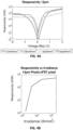
- Illumination of the Photo-JFET with 518nm or 880nm light causes the JFET channel to turn on. With sufficient illuminating irradiance, the total current produced by the Photo-JFET pixel is orders of magnitude higher than the primary photocurrent produced by a reverse biased photodiode ( FIG. 3 ). At low irradiance of ⁇ 10 uW/mm 2 , the photoresponsivity is less than 1 A/W, equivalent to a simple photodiode. However, as the light power increases, the effective responsivity rises to 100 A/W with voltage bias ( FIG. 4 ).
- the required irradiance of 850nm light to turn on the JFET channel is around 50uW/mm 2 for a 13 ⁇ m pixel and 8uW/mm 2 for a 40 ⁇ m pixel.
- Both 13 ⁇ m and 40 ⁇ m Photo-JFET pixels have similar performance in terms of photoresponsivity. For both devices, gain reaches the peak value then decreases with increasing irradiance, in agreement with the device model.
- FIG. 4A shows voltage dependence of responsivity of a 13 ⁇ m photo-JFET pixel and FIG. 4B shows Responsivity of a 13 ⁇ m diameter pixel vs. NIR irradiance at 2V bias.
- Retina was placed over stimulating electrodes ganglion cell side up.
- Retinal ganglion cells (RGCs) were visualized using IR differential interference contrast video microscopy. Recording electrodes were pulled from borosilicate capillary glass to have a final resistance of 4-5 M ⁇ and filled with Ames medium. Action potentials in RGCs were recorded in the loose patch configuration using a Multiclamp 700b (Molecular Devices). Signals were filtered at 4kHz (4-pole Bessel), digitized at 20 kHz with an ITC-18 (HEKA Electronik) and saved to a PC for offline analysis.
- Bias was applied to the circuit for 5ms at +2V (anodal) followed by 5ms at -2V (cathodal) while the pixel was kept dark or illuminated (360 ⁇ W/mm 2 or 3.6mW/mm 2 ).
- RGC action potentials were observed and counted within the first 40ms following the onset of the stimulus. Each stimulation condition was repeated for 10 consecutive trials separated by 9 seconds and spike counts were averaged for each cell.
- FIG. 5 shows an overview of the in vitro experiment to demonstrate retinal stimulation with Photo-JFET pixels.
- FIG. 5A shows a diagram of the circuit to connect Photo-JFET pixels on chip to neural stimulation electrodes and the instrumentation used to record stimulated action potentials from retinal neurons.
- FIG. 5B shows a 10x microscope image of Rd10 retina atop of PEDOT/IrOx electrode on transparent substrate with a glass micropipette electrode used to loose patch RGC to record action potentials.
- FIG. 5C shows spiking behavior recorded from RGC in response to electrical stimulation driven by Photo-JFET pixels.
- FIG. 5D shows a comparison of spikes elicited by Photo-JFET stimulation under dark and NIR illumination, with in vitro retinal stimulation with 13 ⁇ m Photo-JFET pixel at 360 ⁇ W/mm 2 and 3.6mW/mm 2 .
- a novel architecture has been proposed consisting of a vertical photo-junction field-effect-transistor for optoelectronic retinal implants.
- the Photo-JFET design combines the functions of light sensing and gain that addresses the critical design goal for retinal prosthesis of minimizing pixel size to enable high visual acuity.
- the design was successfully realized by microfabrication of silicon Photo-JFET pixels of 13 ⁇ m and 40 ⁇ m diameter.
- the device photoresponse was measured under visible and NIR irradiance and demonstrating characteristic JFET gain behavior ( FIG. 3 ).
- the measured FET photoresponsivity ( FIG. 4B ) corresponded with the calculated theoretical gain behavior for representative pixel size ( FIG. 2C ).
- Photo-JFET pixels are responsive to visible light, the irradiance of visible light required (>14 ⁇ W/mm 2 ) for sufficient retinal stimulation current is well outside the range of typical retinal irradiance and the safe exposure limit of 518nm light. Therefore, similar to existing technologies, a NIR source can be used to optically address Photo-JFET array to encode stimulation parameters such as stimulation current and spatial contrast [8,16].
- the maximum permissible irradiance of 850nm on the cornea and lens is 200 ⁇ W/mm 2 for continuous exposure over 8 hours and 5.9mW/mm 2 for 5ms of pulsed exposure at 20Hz repetition [23,24].
- Photo-JFET pixels can produce sufficient current for stimulation within a safe range of NIR light at 850nm ( Fig. 6 ).
- devices can be optically addressed with less NIR irradiance if the pixel size is expanded.
- Photo-JFET devices produce similar total output current at equivalent incident light power since the performance is proportional to pixel circumference and primary photocurrent (Eqn. (4)).
- Eqn. (4) primary photocurrent
- the spatial resolution of a retinal prosthesis is determined by the center-to-center electrode spacing in the array. Specifically, for an implantable MPDA, electrode spacing depends directly on the photosensing area required per individual pixel to produce sufficient current for stimulation. The reported minimum current required to stimulate a retinal neuron in vitro with microelectrodes is ⁇ 500nA for anodic-first stimulation and slightly higher at ⁇ 800nA for cathodic-first at 10ms pulse duration. [22].
- a 13 ⁇ m Photo-JFET pixel can utilize phototransistive gain to produce enough current beyond threshold for neural stimulation ( Fig. 6 ).
- a photodiode only approach requires larger pixel of at least 40 ⁇ m and NIR light nearing maximum permissible exposure (MPE) to reach stimulation threshold.
- MPE NIR light nearing maximum permissible exposure
- a Photo-JFET pixel-based prosthesis may achieve higher spatial resolution beyond that of existing MPDA technologies.
- Electrochemical crosstalk will determine the actual spatial resolution of the array.
- Crosstalk arises from overlapping signals from adjacent electrodes due to the spread of current density in an ionic environment. A closer apposition of the stimulating electrode to the retinal neural tissue can lower stimulation threshold and help preserve the spatial resolution of a high-density array.
- a Photo-JFET array can be modified to mitigate the effect of crosstalk.
- the silicon mesa comprising the Photo-JFET pixel can be etched from the epitaxial silicon substrate to form a micropillar with a vertical height on the order of 10-50 ⁇ m.
- An implantable version of the Photo-JFET prosthesis may consist of an array of pixels on silicon die attached to a flexible polymer substrate, connected via an inductive link to an external power source to supply the voltage bias.
- Photo-JFET pixels of 13 ⁇ m diameter can be arrayed at 15 ⁇ m pitch, enabling a prosthetic spatial resolution of ⁇ 20/60 which may offer a substantial improvement in clinical visual acuity for patients with degenerative retinal disease.
- FIG. 6 shows a comparison of measured current produced by 13 ⁇ m Photo-JFET pixels versus theoretical current of passive photodiode pixels at 13 ⁇ m and 40 ⁇ m diameter under the same illumination conditions with NIR light (850nm). A responsivity of 0.4 A/W is assumed for passive photodiodes [25].
- a novel vertical junction field-effect -transistor architecture has been developed that achieves photosensing, gain, and neural stimulation in a compact pixel size for high visual acuity retinal prosthesis.
- the design was realized by a vertically integrated back-to-back diode structure in parallel with a sidewall FET.
- Photo-JFET pixels were successfully fabricated at pixel dimensions approaching cellular scale.
- a simple bias mechanism and optical addressing using NIR light produce a broad range current for neural stimulation per pixel. It was demonstrated in a proof-of-concept experiment that a single Photo-JFET pixel can effectively stimulate retinal neurons in an in vitro model of degenerative retinal disease.
- the Photo-JFET design allows for smaller pixel sizes with improved functionality versus passive microphotodiode arrays. This subject disclosure demonstrates an important development towards high visual acuity retinal prostheses that may help restore clinically meaningful vision, better than 20/100 in patients with degenerative retinal disease.
- the specification may have presented the method and/or process of the present subject disclosure as a particular sequence of steps. However, to the extent that the method or process does not rely on the particular order of steps set forth herein, the method or process should not be limited to the particular sequence of steps described. As one of ordinary skill in the art would appreciate, other sequences of steps may be possible.
Landscapes
- Health & Medical Sciences (AREA)
- General Health & Medical Sciences (AREA)
- Veterinary Medicine (AREA)
- Biomedical Technology (AREA)
- Nuclear Medicine, Radiotherapy & Molecular Imaging (AREA)
- Radiology & Medical Imaging (AREA)
- Life Sciences & Earth Sciences (AREA)
- Engineering & Computer Science (AREA)
- Public Health (AREA)
- Animal Behavior & Ethology (AREA)
- Ophthalmology & Optometry (AREA)
- Heart & Thoracic Surgery (AREA)
- Cardiology (AREA)
- Neurology (AREA)
- Prostheses (AREA)
- Solid State Image Pick-Up Elements (AREA)
Claims (10)
- Retinaprothese, umfassend:einen vertikal integrierten lichtempfindlichen Sperrschicht-Feldeffekttransistor (Photo-JFET), der eine Siliciummesa aufweist; undeine Neurostimulationselektrode;dadurch gekennzeichnet, dassder Photo-JFET ein Paar von unmittelbar aufeinanderfolgenden p/n-Dioden umfasst, die entweder in einer N-P-N- oder P-N-P-Konfiguration parallel zu einem Seitenwand-Sperrschicht-Feldeffekttransistor konfiguriert sind, wobei ein dielektrischer Film auf einer Seitenwand der Siliciummesa abgeschieden ist, um eine schwache Inversionsschicht entlang der vertikalen Kante der Mittelschicht der unmittelbar aufeinanderfolgenden Dioden zu erzeugen, wobei ein vertikaler Kanal entlang der Mesa-Seitenwand gebildet wird.
- Retinaprothese nach Anspruch 1, wobei die Siliciumpixelmesa ferner einen Photodetektor integriert.
- Retinaprothese nach Anspruch 2, wobei die Siliciumpixelmesa ferner einen Verstärker integriert.
- Retinaprothese nach Anspruch 3, wobei die Siliciumpixelmesa ferner einen Neuro-Elektrodenstimulator integriert.
- Retinaprothese nach Anspruch 4, die ferner einen dielektrischen Film umfasst, der auf der Siliciumpixelmesa angeordnet ist.
- Retinaprothese nach Anspruch 1, wobei ein Stromstärkenbereich von 0,1 bis 100 µA erzeugt wird.
- Retinaprothese nach Anspruch 1, die ferner ein 13-µm-Pixel umfasst.
- Retinaprothese nach Anspruch 1, die ferner eine Anordnung von 13-µm-Pixeln umfasst.
- Retinaprothese nach Anspruch 1, die ferner ein 40-µm-Pixel umfasst.
- Retinaprothese nach Anspruch 1, die ferner eine Anordnung von 40-µm-Pixeln umfasst.
Applications Claiming Priority (2)
| Application Number | Priority Date | Filing Date | Title |
|---|---|---|---|
| US201962926411P | 2019-10-25 | 2019-10-25 | |
| PCT/US2020/057423 WO2021081533A1 (en) | 2019-10-25 | 2020-10-26 | Retinal prostheses |
Publications (3)
| Publication Number | Publication Date |
|---|---|
| EP4048201A1 EP4048201A1 (de) | 2022-08-31 |
| EP4048201A4 EP4048201A4 (de) | 2023-11-22 |
| EP4048201B1 true EP4048201B1 (de) | 2025-05-21 |
Family
ID=75585523
Family Applications (1)
| Application Number | Title | Priority Date | Filing Date |
|---|---|---|---|
| EP20879132.7A Active EP4048201B1 (de) | 2019-10-25 | 2020-10-26 | Retinale prothesen |
Country Status (4)
| Country | Link |
|---|---|
| US (1) | US12239834B2 (de) |
| EP (1) | EP4048201B1 (de) |
| CA (1) | CA3155584A1 (de) |
| WO (1) | WO2021081533A1 (de) |
Families Citing this family (1)
| Publication number | Priority date | Publication date | Assignee | Title |
|---|---|---|---|---|
| US20220387786A1 (en) * | 2021-06-04 | 2022-12-08 | Nanovision Biosciences, Inc. | High visual acuity, high sensitivity light switchable neural stimulator array for implantable retinal prosthesis |
Family Cites Families (17)
| Publication number | Priority date | Publication date | Assignee | Title |
|---|---|---|---|---|
| JP3842309B2 (ja) * | 1995-02-16 | 2006-11-08 | 浜松ホトニクス株式会社 | 半導体バルク結合型素子を用いた信号相関処理装置 |
| US7009647B1 (en) * | 2000-04-24 | 2006-03-07 | Ess Technology, Inc. | CMOS imager having a JFET adapted to detect photons and produce an amplified electrical signal |
| US7447547B2 (en) * | 2003-02-14 | 2008-11-04 | The Board Of Trustees Of The Leland Stanford Junior University | Neural prosthesis based on photomechanical deflectors and tactile sensory cells |
| US20070241377A1 (en) | 2006-04-12 | 2007-10-18 | Semicoa | Back-illuminated photo-transistor arrays for computed tomography and other imaging applications |
| US8273610B2 (en) * | 2010-11-18 | 2012-09-25 | Monolithic 3D Inc. | Method of constructing a semiconductor device and structure |
| US9795787B2 (en) * | 2011-05-16 | 2017-10-24 | Seoul National University R&Db Foundation | Retinal prosthesis system using nanowire light detector, and manufacturing method thereof |
| US8415771B1 (en) * | 2012-05-25 | 2013-04-09 | LuxVue Technology Corporation | Micro device transfer head with silicon electrode |
| US9737710B2 (en) * | 2014-06-30 | 2017-08-22 | Long-Sheng Fan | Methods and apparatuses for configuring artificial retina devices |
| US10207108B2 (en) * | 2014-10-22 | 2019-02-19 | Oculeve, Inc. | Implantable nasal stimulator systems and methods |
| WO2016079263A1 (fr) * | 2014-11-19 | 2016-05-26 | Chambre De Commerce Et D'industrie De Region Paris Ile De France (Esiee Paris) | Procede de fabrication d'implant pour la stimulation electrique focale d'une structure nerveuse |
| US20160256677A1 (en) * | 2015-03-02 | 2016-09-08 | The Board Of Trustees Of The University Of Alabama | Flexible digital image sensor |
| CN107635620B (zh) * | 2015-05-12 | 2021-06-08 | Pixium视野股份公司 | 具有缠绕电阻器的光敏像素结构 |
| TR201612947A2 (tr) * | 2016-09-09 | 2018-03-21 | Utku Bueyueksahin | Biyomekatronik veri iletim sistemleri. |
| US11439822B2 (en) * | 2017-03-31 | 2022-09-13 | ECOLE POLYTECHNIQUE FéDéRALE DE LAUSANNE | Polymer-based optoelectronic interface and methods for its manufacture |
| JP2020519379A (ja) * | 2017-05-08 | 2020-07-02 | ラムダヴィジョン インコーポレイテッド | 網膜細胞を刺激し、視力喪失を処置するための方法 |
| FR3072564B1 (fr) | 2017-10-25 | 2019-10-18 | Universite De Lille 1 Sciences Et Technologies | Capteur optique |
| US11497913B1 (en) * | 2018-02-28 | 2022-11-15 | Bionic Eye Technologies, Inc. | Micro-fabricated electrode arrays with flexible substrate for highly charge-efficient and selective stimulation of nerve tissue |
-
2020
- 2020-10-26 US US17/080,779 patent/US12239834B2/en active Active
- 2020-10-26 CA CA3155584A patent/CA3155584A1/en active Pending
- 2020-10-26 EP EP20879132.7A patent/EP4048201B1/de active Active
- 2020-10-26 WO PCT/US2020/057423 patent/WO2021081533A1/en not_active Ceased
Also Published As
| Publication number | Publication date |
|---|---|
| US20210121685A1 (en) | 2021-04-29 |
| CA3155584A1 (en) | 2021-04-29 |
| WO2021081533A1 (en) | 2021-04-29 |
| EP4048201A4 (de) | 2023-11-22 |
| US12239834B2 (en) | 2025-03-04 |
| EP4048201A1 (de) | 2022-08-31 |
Similar Documents
| Publication | Publication Date | Title |
|---|---|---|
| EP2582324B1 (de) | Vertikale nanodrahtarrays von ultrahoher lichtempfindlichkeit für netzhautprothesen | |
| US6389317B1 (en) | Multi-phasic microphotodetector retinal implant with variable voltage and current capability | |
| US10603493B2 (en) | Integrated nanowire array devices for detecting and/or applying electrical signals to tissue | |
| US7610098B2 (en) | Charge-integrating retinal prosthesis and method | |
| Ha et al. | Towards high-resolution retinal prostheses with direct optical addressing and inductive telemetry | |
| AU2001243665A1 (en) | Multi-phasic microphotodetector retinal implant with variable voltage and current capability and apparatus for insertion | |
| Li et al. | 2D semiconductor based flexible photoresponsive ring oscillators for artificial vision pixels | |
| US12239834B2 (en) | Retinal prostheses | |
| Damle et al. | Vertically integrated photo junction-field-effect transistor pixels for retinal prosthesis | |
| Tanaka et al. | Fully implantable retinal prosthesis chip with photodetector and stimulus current generator | |
| Khraiche et al. | Ultra-high photosensitivity silicon nanophotonics for retinal prosthesis: electrical characteristics | |
| US20220387786A1 (en) | High visual acuity, high sensitivity light switchable neural stimulator array for implantable retinal prosthesis | |
| Ye et al. | Implantable Nongenetic Optoelectronic Biointerfaces for Neuromodulation | |
| Xing et al. | Research progress of subretinal implant based on electronic stimulation | |
| 박정환 | Low Power Design and LCP Packaging for Photodiode-based Retinal Prosthesis System |
Legal Events
| Date | Code | Title | Description |
|---|---|---|---|
| STAA | Information on the status of an ep patent application or granted ep patent |
Free format text: STATUS: THE INTERNATIONAL PUBLICATION HAS BEEN MADE |
|
| PUAI | Public reference made under article 153(3) epc to a published international application that has entered the european phase |
Free format text: ORIGINAL CODE: 0009012 |
|
| STAA | Information on the status of an ep patent application or granted ep patent |
Free format text: STATUS: REQUEST FOR EXAMINATION WAS MADE |
|
| 17P | Request for examination filed |
Effective date: 20220524 |
|
| AK | Designated contracting states |
Kind code of ref document: A1 Designated state(s): AL AT BE BG CH CY CZ DE DK EE ES FI FR GB GR HR HU IE IS IT LI LT LU LV MC MK MT NL NO PL PT RO RS SE SI SK SM TR |
|
| DAV | Request for validation of the european patent (deleted) | ||
| DAX | Request for extension of the european patent (deleted) | ||
| A4 | Supplementary search report drawn up and despatched |
Effective date: 20231023 |
|
| RIC1 | Information provided on ipc code assigned before grant |
Ipc: A61N 1/05 20060101ALI20231017BHEP Ipc: A61F 2/14 20060101AFI20231017BHEP |
|
| GRAP | Despatch of communication of intention to grant a patent |
Free format text: ORIGINAL CODE: EPIDOSNIGR1 |
|
| STAA | Information on the status of an ep patent application or granted ep patent |
Free format text: STATUS: GRANT OF PATENT IS INTENDED |
|
| RIC1 | Information provided on ipc code assigned before grant |
Ipc: A61N 1/05 20060101ALI20241203BHEP Ipc: A61F 2/14 20060101AFI20241203BHEP |
|
| INTG | Intention to grant announced |
Effective date: 20241216 |
|
| GRAS | Grant fee paid |
Free format text: ORIGINAL CODE: EPIDOSNIGR3 |
|
| GRAA | (expected) grant |
Free format text: ORIGINAL CODE: 0009210 |
|
| STAA | Information on the status of an ep patent application or granted ep patent |
Free format text: STATUS: THE PATENT HAS BEEN GRANTED |
|
| RAP3 | Party data changed (applicant data changed or rights of an application transferred) |
Owner name: NANOVISION BIOSCIENCES, INC. |
|
| AK | Designated contracting states |
Kind code of ref document: B1 Designated state(s): AL AT BE BG CH CY CZ DE DK EE ES FI FR GB GR HR HU IE IS IT LI LT LU LV MC MK MT NL NO PL PT RO RS SE SI SK SM TR |
|
| RAP1 | Party data changed (applicant data changed or rights of an application transferred) |
Owner name: THE REGENTS OF THE UNIVERSITY OF CALIFORNIA Owner name: NANOVISION BIOSCIENCES, INC. |
|
| REG | Reference to a national code |
Ref country code: GB Ref legal event code: FG4D |
|
| REG | Reference to a national code |
Ref country code: CH Ref legal event code: EP |
|
| REG | Reference to a national code |
Ref country code: DE Ref legal event code: R096 Ref document number: 602020051832 Country of ref document: DE |
|
| REG | Reference to a national code |
Ref country code: IE Ref legal event code: FG4D |
|
| P01 | Opt-out of the competence of the unified patent court (upc) registered |
Free format text: CASE NUMBER: APP_25816/2025 Effective date: 20250530 |
|
| REG | Reference to a national code |
Ref country code: NL Ref legal event code: MP Effective date: 20250521 |
|
| PG25 | Lapsed in a contracting state [announced via postgrant information from national office to epo] |
Ref country code: FI Free format text: LAPSE BECAUSE OF FAILURE TO SUBMIT A TRANSLATION OF THE DESCRIPTION OR TO PAY THE FEE WITHIN THE PRESCRIBED TIME-LIMIT Effective date: 20250521 Ref country code: ES Free format text: LAPSE BECAUSE OF FAILURE TO SUBMIT A TRANSLATION OF THE DESCRIPTION OR TO PAY THE FEE WITHIN THE PRESCRIBED TIME-LIMIT Effective date: 20250521 Ref country code: PT Free format text: LAPSE BECAUSE OF FAILURE TO SUBMIT A TRANSLATION OF THE DESCRIPTION OR TO PAY THE FEE WITHIN THE PRESCRIBED TIME-LIMIT Effective date: 20250922 |
|
| REG | Reference to a national code |
Ref country code: LT Ref legal event code: MG9D |
|
| PG25 | Lapsed in a contracting state [announced via postgrant information from national office to epo] |
Ref country code: NO Free format text: LAPSE BECAUSE OF FAILURE TO SUBMIT A TRANSLATION OF THE DESCRIPTION OR TO PAY THE FEE WITHIN THE PRESCRIBED TIME-LIMIT Effective date: 20250821 Ref country code: GR Free format text: LAPSE BECAUSE OF FAILURE TO SUBMIT A TRANSLATION OF THE DESCRIPTION OR TO PAY THE FEE WITHIN THE PRESCRIBED TIME-LIMIT Effective date: 20250822 |
|
| PG25 | Lapsed in a contracting state [announced via postgrant information from national office to epo] |
Ref country code: NL Free format text: LAPSE BECAUSE OF FAILURE TO SUBMIT A TRANSLATION OF THE DESCRIPTION OR TO PAY THE FEE WITHIN THE PRESCRIBED TIME-LIMIT Effective date: 20250521 Ref country code: PL Free format text: LAPSE BECAUSE OF FAILURE TO SUBMIT A TRANSLATION OF THE DESCRIPTION OR TO PAY THE FEE WITHIN THE PRESCRIBED TIME-LIMIT Effective date: 20250521 |
|
| PG25 | Lapsed in a contracting state [announced via postgrant information from national office to epo] |
Ref country code: BG Free format text: LAPSE BECAUSE OF FAILURE TO SUBMIT A TRANSLATION OF THE DESCRIPTION OR TO PAY THE FEE WITHIN THE PRESCRIBED TIME-LIMIT Effective date: 20250521 |
|
| PGFP | Annual fee paid to national office [announced via postgrant information from national office to epo] |
Ref country code: GB Payment date: 20250924 Year of fee payment: 6 |
|
| PG25 | Lapsed in a contracting state [announced via postgrant information from national office to epo] |
Ref country code: HR Free format text: LAPSE BECAUSE OF FAILURE TO SUBMIT A TRANSLATION OF THE DESCRIPTION OR TO PAY THE FEE WITHIN THE PRESCRIBED TIME-LIMIT Effective date: 20250521 |
|
| PGFP | Annual fee paid to national office [announced via postgrant information from national office to epo] |
Ref country code: FR Payment date: 20250923 Year of fee payment: 6 |
|
| PG25 | Lapsed in a contracting state [announced via postgrant information from national office to epo] |
Ref country code: RS Free format text: LAPSE BECAUSE OF FAILURE TO SUBMIT A TRANSLATION OF THE DESCRIPTION OR TO PAY THE FEE WITHIN THE PRESCRIBED TIME-LIMIT Effective date: 20250821 |
|
| PG25 | Lapsed in a contracting state [announced via postgrant information from national office to epo] |
Ref country code: IS Free format text: LAPSE BECAUSE OF FAILURE TO SUBMIT A TRANSLATION OF THE DESCRIPTION OR TO PAY THE FEE WITHIN THE PRESCRIBED TIME-LIMIT Effective date: 20250921 |
|
| PG25 | Lapsed in a contracting state [announced via postgrant information from national office to epo] |
Ref country code: LV Free format text: LAPSE BECAUSE OF FAILURE TO SUBMIT A TRANSLATION OF THE DESCRIPTION OR TO PAY THE FEE WITHIN THE PRESCRIBED TIME-LIMIT Effective date: 20250521 |
|
| REG | Reference to a national code |
Ref country code: AT Ref legal event code: MK05 Ref document number: 1796150 Country of ref document: AT Kind code of ref document: T Effective date: 20250521 |
|
| PGFP | Annual fee paid to national office [announced via postgrant information from national office to epo] |
Ref country code: DE Payment date: 20250924 Year of fee payment: 6 |
|
| PG25 | Lapsed in a contracting state [announced via postgrant information from national office to epo] |
Ref country code: SM Free format text: LAPSE BECAUSE OF FAILURE TO SUBMIT A TRANSLATION OF THE DESCRIPTION OR TO PAY THE FEE WITHIN THE PRESCRIBED TIME-LIMIT Effective date: 20250521 Ref country code: DK Free format text: LAPSE BECAUSE OF FAILURE TO SUBMIT A TRANSLATION OF THE DESCRIPTION OR TO PAY THE FEE WITHIN THE PRESCRIBED TIME-LIMIT Effective date: 20250521 Ref country code: AT Free format text: LAPSE BECAUSE OF FAILURE TO SUBMIT A TRANSLATION OF THE DESCRIPTION OR TO PAY THE FEE WITHIN THE PRESCRIBED TIME-LIMIT Effective date: 20250521 |
|
| PG25 | Lapsed in a contracting state [announced via postgrant information from national office to epo] |
Ref country code: CZ Free format text: LAPSE BECAUSE OF FAILURE TO SUBMIT A TRANSLATION OF THE DESCRIPTION OR TO PAY THE FEE WITHIN THE PRESCRIBED TIME-LIMIT Effective date: 20250521 |
|
| PG25 | Lapsed in a contracting state [announced via postgrant information from national office to epo] |
Ref country code: EE Free format text: LAPSE BECAUSE OF FAILURE TO SUBMIT A TRANSLATION OF THE DESCRIPTION OR TO PAY THE FEE WITHIN THE PRESCRIBED TIME-LIMIT Effective date: 20250521 |
|
| PG25 | Lapsed in a contracting state [announced via postgrant information from national office to epo] |
Ref country code: SK Free format text: LAPSE BECAUSE OF FAILURE TO SUBMIT A TRANSLATION OF THE DESCRIPTION OR TO PAY THE FEE WITHIN THE PRESCRIBED TIME-LIMIT Effective date: 20250521 |
|
| PG25 | Lapsed in a contracting state [announced via postgrant information from national office to epo] |
Ref country code: IT Free format text: LAPSE BECAUSE OF FAILURE TO SUBMIT A TRANSLATION OF THE DESCRIPTION OR TO PAY THE FEE WITHIN THE PRESCRIBED TIME-LIMIT Effective date: 20250521 |
|
| PG25 | Lapsed in a contracting state [announced via postgrant information from national office to epo] |
Ref country code: RO Free format text: LAPSE BECAUSE OF FAILURE TO SUBMIT A TRANSLATION OF THE DESCRIPTION OR TO PAY THE FEE WITHIN THE PRESCRIBED TIME-LIMIT Effective date: 20250521 |
|
| REG | Reference to a national code |
Ref country code: DE Ref legal event code: R097 Ref document number: 602020051832 Country of ref document: DE |
|
| PLBE | No opposition filed within time limit |
Free format text: ORIGINAL CODE: 0009261 |
|
| STAA | Information on the status of an ep patent application or granted ep patent |
Free format text: STATUS: NO OPPOSITION FILED WITHIN TIME LIMIT |
|
| REG | Reference to a national code |
Ref country code: CH Ref legal event code: L10 Free format text: ST27 STATUS EVENT CODE: U-0-0-L10-L00 (AS PROVIDED BY THE NATIONAL OFFICE) Effective date: 20260402 |
|
| 26N | No opposition filed |
Effective date: 20260224 |