EP4047751A1 - Millimeterwellenantenne für 5g-anwendungen und fahrzeug mit einer solchen antenne - Google Patents
Millimeterwellenantenne für 5g-anwendungen und fahrzeug mit einer solchen antenne Download PDFInfo
- Publication number
- EP4047751A1 EP4047751A1 EP22157466.8A EP22157466A EP4047751A1 EP 4047751 A1 EP4047751 A1 EP 4047751A1 EP 22157466 A EP22157466 A EP 22157466A EP 4047751 A1 EP4047751 A1 EP 4047751A1
- Authority
- EP
- European Patent Office
- Prior art keywords
- antenna
- layer
- inner layer
- radiating elements
- sublayer
- Prior art date
- Legal status (The legal status is an assumption and is not a legal conclusion. Google has not performed a legal analysis and makes no representation as to the accuracy of the status listed.)
- Granted
Links
Images




Classifications
-
- H—ELECTRICITY
- H01—ELECTRIC ELEMENTS
- H01Q—ANTENNAS, i.e. RADIO AERIALS
- H01Q1/00—Details of, or arrangements associated with, antennas
- H01Q1/27—Adaptation for use in or on movable bodies
- H01Q1/32—Adaptation for use in or on road or rail vehicles
- H01Q1/3208—Adaptation for use in or on road or rail vehicles characterised by the application wherein the antenna is used
- H01Q1/3233—Adaptation for use in or on road or rail vehicles characterised by the application wherein the antenna is used particular used as part of a sensor or in a security system, e.g. for automotive radar, navigation systems
-
- H—ELECTRICITY
- H01—ELECTRIC ELEMENTS
- H01Q—ANTENNAS, i.e. RADIO AERIALS
- H01Q1/00—Details of, or arrangements associated with, antennas
- H01Q1/27—Adaptation for use in or on movable bodies
- H01Q1/32—Adaptation for use in or on road or rail vehicles
-
- H—ELECTRICITY
- H01—ELECTRIC ELEMENTS
- H01Q—ANTENNAS, i.e. RADIO AERIALS
- H01Q1/00—Details of, or arrangements associated with, antennas
- H01Q1/52—Means for reducing coupling between antennas; Means for reducing coupling between an antenna and another structure
- H01Q1/521—Means for reducing coupling between antennas; Means for reducing coupling between an antenna and another structure reducing the coupling between adjacent antennas
-
- H—ELECTRICITY
- H01—ELECTRIC ELEMENTS
- H01Q—ANTENNAS, i.e. RADIO AERIALS
- H01Q13/00—Waveguide horns or mouths; Slot antennas; Leaky-waveguide antennas; Equivalent structures causing radiation along the transmission path of a guided wave
- H01Q13/10—Resonant slot antennas
-
- H—ELECTRICITY
- H01—ELECTRIC ELEMENTS
- H01Q—ANTENNAS, i.e. RADIO AERIALS
- H01Q21/00—Antenna arrays or systems
- H01Q21/0006—Particular feeding systems
- H01Q21/0075—Stripline fed arrays
-
- H—ELECTRICITY
- H01—ELECTRIC ELEMENTS
- H01Q—ANTENNAS, i.e. RADIO AERIALS
- H01Q21/00—Antenna arrays or systems
- H01Q21/0087—Apparatus or processes specially adapted for manufacturing antenna arrays
-
- H—ELECTRICITY
- H01—ELECTRIC ELEMENTS
- H01Q—ANTENNAS, i.e. RADIO AERIALS
- H01Q21/00—Antenna arrays or systems
- H01Q21/06—Arrays of individually energised antenna units similarly polarised and spaced apart
- H01Q21/061—Two dimensional planar arrays
- H01Q21/065—Patch antenna array
-
- H—ELECTRICITY
- H01—ELECTRIC ELEMENTS
- H01Q—ANTENNAS, i.e. RADIO AERIALS
- H01Q9/00—Electrically-short antennas having dimensions not more than twice the operating wavelength and consisting of conductive active radiating elements
- H01Q9/04—Resonant antennas
- H01Q9/0407—Substantially flat resonant element parallel to ground plane, e.g. patch antenna
-
- H—ELECTRICITY
- H01—ELECTRIC ELEMENTS
- H01Q—ANTENNAS, i.e. RADIO AERIALS
- H01Q9/00—Electrically-short antennas having dimensions not more than twice the operating wavelength and consisting of conductive active radiating elements
- H01Q9/04—Resonant antennas
- H01Q9/0407—Substantially flat resonant element parallel to ground plane, e.g. patch antenna
- H01Q9/0414—Substantially flat resonant element parallel to ground plane, e.g. patch antenna in a stacked or folded configuration
-
- H—ELECTRICITY
- H01—ELECTRIC ELEMENTS
- H01Q—ANTENNAS, i.e. RADIO AERIALS
- H01Q9/00—Electrically-short antennas having dimensions not more than twice the operating wavelength and consisting of conductive active radiating elements
- H01Q9/04—Resonant antennas
- H01Q9/0407—Substantially flat resonant element parallel to ground plane, e.g. patch antenna
- H01Q9/045—Substantially flat resonant element parallel to ground plane, e.g. patch antenna with particular feeding means
-
- H—ELECTRICITY
- H01—ELECTRIC ELEMENTS
- H01Q—ANTENNAS, i.e. RADIO AERIALS
- H01Q9/00—Electrically-short antennas having dimensions not more than twice the operating wavelength and consisting of conductive active radiating elements
- H01Q9/04—Resonant antennas
- H01Q9/0407—Substantially flat resonant element parallel to ground plane, e.g. patch antenna
- H01Q9/045—Substantially flat resonant element parallel to ground plane, e.g. patch antenna with particular feeding means
- H01Q9/0457—Substantially flat resonant element parallel to ground plane, e.g. patch antenna with particular feeding means electromagnetically coupled to the feed line
-
- H—ELECTRICITY
- H01—ELECTRIC ELEMENTS
- H01Q—ANTENNAS, i.e. RADIO AERIALS
- H01Q1/00—Details of, or arrangements associated with, antennas
- H01Q1/12—Supports; Mounting means
- H01Q1/22—Supports; Mounting means by structural association with other equipment or articles
- H01Q1/24—Supports; Mounting means by structural association with other equipment or articles with receiving set
- H01Q1/241—Supports; Mounting means by structural association with other equipment or articles with receiving set used in mobile communications, e.g. GSM
Definitions
- the present invention relates to a millimeter-wave antenna for 5G applications, and to a vehicle comprising such antenna.
- the antenna according to the present invention is especially suitable for use in vehicles, such as for example automobiles, buses, trains, commercial vehicles et cetera, and will be described in the following with reference to such applications, however without thereby intending in any way to limit its use in other possible fields of application.
- mmW millimeter-wave
- antennas which include, among their essential components, the radiating elements dedicated to the transceiving of signals, and the control electronics designed to control and appropriately drive the operation of the radiating elements themselves.
- the cost and dimensions of the antennas are negatively affected, rendering their use more difficult, for example in vehicles, such as automobiles, wherein the spaces available for antennas are limited and moreover it is usually necessary to contemporaneously make use of multiple antennas located in different positions due to the extensive presence of metal parts that act as a shield for the antennas themselves.
- the main object of the present invention is to provide a millimeter-wave antenna for 5G applications that makes it possible in particular to solve or at least reduce the problems relating to unwanted reflections of the signals to be transmitted, while requiring a construction structure that is compact and easy to implement at relatively low costs.
- a vehicle typically a vehicle meant for transporting passengers, in particular an automobile, characterized in that it comprises at least one antenna as described below, and in particular as better defined in the appended claims.
- Figure 1 schematically illustrates one possible embodiment of a millimeter-wave antenna according to the invention, indicated as a whole by the reference numeral 1.
- the antenna 1 comprises a multilayer structure stacked vertically along the reference direction indicated in Figure 1 by the reference axis X, said multilayer structure including at least:
- the upper outer layer 10 comprises at least a first dielectric sublayer 12, for example made from ROGERS RO4350B material, and a plurality of first radiating elements 14 suitable for being fed with and radiating the signals to be transmitted.
- the first radiating elements 14 are made of electrically conductive material, for example copper, and are arranged spaced apart from each other on the first dielectric sublayer 12 substantially aligned in sequence along a reference horizontal axis Y that is perpendicular to the axis X.
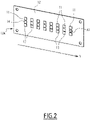
- the first radiating elements 14 are preferably substantially identical to each other and each have a radiating area or surface "A1" measured in a plane transverse to the axis X, that is to say in the plane of the layer itself. For simplicity of illustration, this radiating area is clearly indicated in Figure 2 with oblique lines only for one radiating element 14.
- the first radiating elements 14 are of the type more precisely referred to as "patches", according to the nationally and internationally used term, with each having a substantially regular geometrical configuration, for example square or rectangular or circular.
- the upper outer layer 10 has a second sublayer 18, also referred to hereinafter as the first bonding sublayer 18, for example made from ROGERS RO4450 material, which is capable of enabling bonding of the upper outer layer 10 in its entirety with the layer of the plurality of layers immediately below it.
- This first bonding sublayer 18 has a first thickness S1.
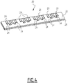
- the multilayer structure of the antenna 1 usefully comprises another inner layer 15, illustrated in Figure 3 , which is bonded to the first bonding sublayer 18, and is therefore interposed between the upper outer layer 10 and the first inner layer 20.
- the first inner layer 20 may be arranged immediately below and directly bonded in its upper part to the first bonding sublayer 18; in this case the further layer 15 is not used.
- the first inner layer 20 comprises at least an own first sublayer of conductive material 22, constituted for example of a copper foil, which is arranged on an own second sublayer of dielectric material 26.
- This second sublayer of dielectric material 26 may be prepared in a manner such as to have adhesive properties and enable bonding with the layer of the plurality of layers immediately there-below, that is to say in the illustrated exemplary embodiment with the second inner layer 30, or it may be combined with some adhesive material added so as to enable it to adhere to the subsequent layer.
- the first inner layer 20 comprises a plurality of through slots 24, having for example a U or C shaped form, which pass through the first sublayer of conductive material 22 and the second sublayer of dielectric material 26 and are suitable for conveying, towards at least the plurality of first radiating elements 14, the feeding signals to be radiated originating from the lower layers of the antenna 1 which will be described hereinafter.
- each through slot 24 is realized on the first inner layer 20 in an underlying position corresponding to the position of the associated first radiating element 14 on the upper outer layer 10.
- each slot 24 extends over the upper horizontal surface of the first inner layer 20 in a manner such that at least one end portion thereof is outside a virtual area obtained by projecting vertically (along the direction of the axis X) onto the first inner layer 20 itself the radiating surface "A1" of the associated first radiating element or alternatively by projecting, again vertically, each slot 24 onto the first inner layer 20.
- each first radiating element 14 there is provided an associated pair of through slots 24, the two through slots 24 of each pair being formed on the first inner layer 20 in an underlying position corresponding to the position of the associated first radiating element 14 on the upper outer layer 10.
- the two slots of each pair of through slots 24, having for example a C or U shaped form, are arranged substantially perpendicular to each other.
- each slot 24 extends over the upper horizontal surface of the first inner layer 20 in a manner such that at least one end portion thereof extends outside a virtual area obtained by projecting vertically onto the first inner layer 20 itself the radiating surface "A1" of the associated first radiating element 14 (or alternatively by projecting, again vertically, each slot 24 onto the first inner layer 20).
- the first inner layer 20 there is defined a plurality of metallized holes 29 which pass through the sublayers 22 and 26.
- the second inner layer 30, which is attached above the sublayer 26, comprises at least an own first dielectric sublayer 32 (also referred to as third dielectric sublayer 32 to better distinguish it from the dielectric layers described previously) on which there is arranged a plurality of conductive lines 34, constituted for example of copper strips, that are suitable for conducting the feeding signals to be radiated at least towards the plurality of first radiating elements 14.
- an own first dielectric sublayer 32 also referred to as third dielectric sublayer 32 to better distinguish it from the dielectric layers described previously
- conductive lines 34 constituted for example of copper strips
- At least one corresponding conductive line 34 is associated with each radiating element.
- the third dielectric sublayer 32 acts as a bonding layer and therefore has adhesive properties or includes adhesive material in order to enable bonding with the layer of the plurality of layers immediately below the inner layer 30, that is to say in the exemplary embodiment illustrated with the further layer 40.
- the third dielectric sublayer 32 which may be made of or comprise for example ROGER RO4450 material, has an overall thickness S2 equal to or greater than the thickness S1 of the first bonding layer 18; in this manner, an improvement in the adapting or "matching" of the signals is advantageously obtained.
- the plurality of conductive lines 34 comprises for each first radiating element 14 a corresponding pair of conductive lines 34 associated therewith, and having for example shapes that differ from each other.
- each pair of conductive lines 34 comprises a first conductive line 34a, formed for example by a copper strip having a substantially rectilinear development, that is capable of transmitting to the corresponding first radiating element 14 the feeding signals to be radiated in a first direction of polarisation, and a second conductive line 34b, for example formed by an L-shaped copper strip, that is capable of transmitting to the said corresponding first radiating element 14, the feeding signals to be radiated in a second direction of polarisation which is different from the first direction.
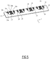
- These directions may be, for example, a first direction along the reference axis Z and a second direction along the reference axis Y, illustrated in Figure 5 .
- the third inner layer 30 as well comprises metallized holes 29 that pass through its sublayers 34 and 32 and are each vertically aligned with a corresponding metallized through hole 29 created on the first inner layer 20; in Figure 5 , for illustrative purposes, the metallized through holes 29 have been shown so that to clearly evidence the shape of through channels or cylinders.
- each conducting line 34 extends over the plane of the sublayer 32 with the metallized holes 29 being arranged alongside on both edges and replicating the path of an associated conducting line 34.
- the conductive lines 34a and 34b of adjacent pairs of lines 34 are arranged in a mutually inverted sequence relative to each other. Furthermore, each line may be flipped to mirror-image or by 180° in the plane of the layer 30 itself, relative to the analogous preceding line.
- the inner layer 30 there is arranged: firstly, the first strip 34a that is capable of transmitting to the associated first radiating element 14 the feeding signals to be radiated in the first direction of polarisation; and then successively, the second conductive line 34b that is capable of transmitting to the same first radiating element 14 the feeding signals to be radiated in the second direction of polarisation.
- the second conductive strip 34b that is capable of transmitting to this subsequent radiating element 14 the feeding signals to be radiated in the second direction of polarisation, which is arranged with the L-shaped form flipped by 180° in the plane of the layer 30 relative to the analogous second line 34b of the preceding pair of lines; then, there is arranged the first line 34a (again flipped to mirror-image or by 180° relative to the analogous first line 34a of the preceding pair) that is capable of transmitting to the same subsequent radiating element 14 the feeding signals to be radiated in the first direction of polarisation.
- the inversion of the positioning order between the first strip 34a and the second strip 34b with any relevant flipping relative to the analogous lines of the preceding pair is regularly repeated at each subsequent radiating element 14 relative to the preceding one.
- one or more of the conductive lines 34 comprise each at least one section of line derived in parallel along the corresponding conductive line 34, preferably arranged to be coincident with the transition zone which in the exemplary embodiment happens to be close to the outer edge of the layer, but which in general could be found within a wider layer, and in particular to be coincident with the transition of a radiofrequency signal, suitable for shifting the signal itself onto a different layer of the antenna, without introducing significant losses.
- This derived section makes it possible to artificially introduce alterations that serve to further enhance the so-called "matching" of the signal transition zones.
- This derived section of line may be constituted, for example, by a further portion of strip, and is illustrated in Figure 5 by the reference numeral 34c only for one pair of conductive lines 34 for the sake of simplicity of description.
- the further layer 40 which is arranged below and is adjacent to the second inner layer 30, comprises at least an own first sublayer of conductive material 42 (hereinafter also referred to as second conductive sublayer 42 so as to distinguish it from the preceding sublayer 22), constituted for example of a copper foil, which is arranged on an own second dielectric sublayer 46 (hereinafter also referred to as fourth dielectric sublayer 46 so as to distinguish it from the previously described dielectric layers).
- second conductive sublayer 42 so as to distinguish it from the preceding sublayer 22
- fourth dielectric sublayer 46 so as to distinguish it from the previously described dielectric layers
- the fourth dielectric sublayer 46 as well may be made directly from a material having adhesive properties or be associated with added adhesive material.
- one the further layer 40 there is defined a plurality of first through openings 44 passing through its sublayers 42 and 46.
- each of said first through openings 44 is formed on the layer 40, and in particular on the sublayer of conductive material 42, in a position corresponding to the position of at least one associated through slot 24 of the plurality of through slots 24 defined on the first sublayer of conductive material 22 of the first inner layer 20.
- each first through opening 44 delimits an area of through-passage "B", measured transversely relative to the reference axis X, which is substantially equal to at least ⁇ 2 /4, that is to say at least a quarter of the square of the wavelength A measured in the dielectric material formed by the assembly of the third dielectric sublayer 32 immediately above the sublayer of conductive material 42 and the fourth dielectric sublayer 46 immediately below the sublayer of conductive material 42.
- the further layer 40 as well comprises metallised holes 29 which pass through at least its sublayer 42 and are arranged on parallel rows that are each aligned with a corresponding metallized through hole 29 created on the first inner layer 20 and on the second inner layer 30.
- the multilayer structure of the antenna 1 according to the invention usefully includes at least one other inner layer, denoted in Figures 1 and 2 by the reference numeral 15 which is interposed between the upper outer layer 10 and the first inner layer 20, and is in particular bonded to the first bonding layer 18 there-above.
- the inner layer 15 comprises at least an own dielectric sublayer 17, hereinafter also referred to as a further dielectric sublayer 17, which also made for example from ROGERS RO4350B material, and a plurality of second radiating elements 16 arranged spaced apart from each other and suitable for being fed with and radiating the signals to be transmitted.
- a further dielectric sublayer 17 which also made for example from ROGERS RO4350B material
- second radiating elements 16 arranged spaced apart from each other and suitable for being fed with and radiating the signals to be transmitted.
- the inner layer 15 also comprises a further bonding sublayer 19, for example made from ROGERS RO4450 material, which is capable of enabling the bonding of the inner layer 15 to the underlying first inner layer 20.
- a further bonding sublayer 19 for example made from ROGERS RO4450 material, which is capable of enabling the bonding of the inner layer 15 to the underlying first inner layer 20.
- the second radiating elements 16 are made of electrically conductive material, for example copper, and are arranged spaced apart from each other on the further dielectric sublayer 17, substantially aligned as well along the reference axis Y.
- each second radiating element 16 is placed below and substantially aligned, at a certain distance, with a corresponding first radiating element 14.
- each second radiating element 16 there is at least one conductive line 34, in particular at least the same conductive line 34 that is associated with the corresponding first radiating element 14 positioned there-above.
- each radiating element 16 is associated with a pair of conductive lines 34a and 34b; hence, each pair of conductive lines 34 is associated both with a corresponding second radiating element 16 as well as with the first radiating element 14 arranged above the said corresponding second radiating element 16.
- the second radiating elements 16 are preferably substantially identical to each other and each extend over a radiating area or surface "A2" (for simplicity of illustration clearly indicated in Figure 1 with oblique lines only for one radiating element 16) and in the illustrated embodiment they are also of the so-called "patch" type.
- each second radiating element 16 has a geometric configuration that is substantially regular, for example square, rectangular or circular.
- the second radiating elements 16 have each a respective radiation area A2, also measured on a plane transverse to the axis X, that is at most equal to and preferably less than the radiation area A1 of each of the first radiating elements 14.
- the presence of the further layer 15 provided with the second radiating elements 16 makes it possible to appropriately widen the range of operating frequencies of the antenna 1 according to the invention.
- each slot 24 extends over the upper horizontal surface of the first inner layer 20 in a manner such that at least one end portion thereof is outside a virtual area obtained by projecting vertically onto the further inner layer 15 itself the radiating surface "A2" of the associated second radiating element 16 (or alternatively by projecting, again vertically, each slot 24 onto the further inner layer 15).
- each slot 24 has been represented only in Figure 3 by virtually projecting the slots 24 onto the layer 15.
- an analogous configuration occurs in respect of at least one end portion of the slots 24 spilling out of the radiation areas A1 of the first radiating elements 14, even if this illustration has not been replicated in Figure 2 for simplicity.
- the multilayer structure of the antenna 1 may include one or more further layers.
- first additional layer 60 hereinafter indicated as the third inner layer 60
- second additional layer 70 hereinafter indicated as the fourth inner layer 70
- third additional layer 80 hereinafter indicated as the lower outer layer 80
- the antenna 1 in the antenna 1 according to the invention, it is possible to use only one of such additional layers, only two, e.g. the first and second additional layers 60 and 70, or the first and third additional layers 60 and 80, or the second and third additional layers 70 and 80, or all of them as it will be described in the following according to the exemplary configuration depicted in figure 1 .
- the first additional layer or third inner layer 60 is arranged below and is adjacent to the further inner layer 40, for example bonded to the fourth dielectric sublayer 46.
- the third inner layer 60 comprises an own first sublayer of conductive material 62 (hereinafter also referred to as third conductive sublayer 62 so as to distinguish it from the preceding conductive sublayers 22 and 42) which is made for example from a copper foil in order to bring the feed voltages to the control chips of the antenna 1 and is arranged on an own second dielectric sublayer 66 (hereinafter also referred to as fifth dielectric sublayer 66 so as to distinguish it from the previously described dielectric layers) made from a material having adhesive properties or combined with some added adhesive material.
- an own first sublayer of conductive material 62 hereinafter also referred to as third conductive sublayer 62 so as to distinguish it from the preceding conductive sublayers 22 and 42
- an own second dielectric sublayer 66 hereinafter also referred to as fifth dielectric sublayer 66 so as to distinguish it from the previously described dielectric layers
- second through openings 64 which pass through the third conductive sublayer 62 and the fifth dielectric sublayer 66; these second through openings 64 in terms of number and shape thereof, are preferably substantially identical to the first through openings 44, with each of them being substantially aligned with a corresponding first through opening 44 relative to a substantially vertical reference direction defined by the axis X.
- a plurality of metallised through holes are also defined on the third inner layer and in particular only on the third conductive sublayer 62 , analogous to the through holes 29 indicated above, which are also arranged so as to be aligned each with a corresponding metallised through hole 29 formed on the first inner layer 20 and on the further inner layer 40.
- the through holes also pass through the dielectric layer 46 and, seen along the vertical direction defined by the reference axis X, when the structure of the antenna 1 is assembled, form a plurality of through channels that start from the first sublayer of conductive material 22 and terminate in the third sublayer of conductive material 62, as schematically illustrated in dashed line in Figure 1 .
- these channels formed by the vertically aligned through holes 29 may terminate at the second sublayer of conductive material 42.
- the first additional layer 60 it will constitute the lower outer layer of the antenna 1, i.e. the layer located at the lowest position of the stack of layers used.
- the second additional layer or fourth inner sublayer 70 is arranged below and is adjacent to the third inner layer 60, for example bonded to the fifth dielectric sublayer 66.
- the fourth inner layer 70 comprises at least an own first sublayer of conducting material 72 (hereinafter also referred to as fourth conducting sublayer 72 so as to distinguish it from the preceding conducting sublayers 22, 42 and 62), which is made for example from a copper foil that acts as a ground plane, and is arranged on an own second dielectric sublayer 76 (hereinafter also referred to as sixth dielectric sublayer 76 so as to distinguish it from the preceding dielectric sublayers) having adhesive properties.
- fourth conducting sublayer 72 so as to distinguish it from the preceding conducting sublayers 22, 42 and 62
- sixth dielectric sublayer 76 so as to distinguish it from the preceding dielectric sublayers
- these third through openings 74 are preferably substantially identical to the first through openings 44, with each of them being substantially aligned with a corresponding first through opening 44 relative to a substantially vertical reference direction defined by the axis X.
- the first through openings 44 are substantially aligned, along the vertical development of the multilayer structure, with the second through openings 64, and/or with the third through openings 74.
- first through openings 44, the second through openings 64, and the third through openings 74 are substantially aligned with each other along the vertical development of the multilayer structure.
- the second additional layer 70 will be arranged below and adjacent to the further inner layer 40 and it will constitute the lower outer layer of the antenna 1, i.e. the layer located at the lowest position of the stack of layers used.
- the second additional layer 70 will also constitute the lower outer layer of the antenna 1 if both only the first and second additional layers 60 and 70 are used.
- the third additional layer or lower outer layer 80 is arranged below the fourth inner layer 70 and comprises one or more connection tracks, schematically illustrated in Figure 8 by dashed lines 82.
- connection tracks are for example constituted of copper traces arranged coincident with the face of the dielectric sublayer 76 opposite to that on which the conducting sublayer 72 is arranged.
- the connection tracks 82 are capable of being connected with one or more chips (not illustrated) for control and/or conditioning, for example for phase shifting or amplification, of the feeding signals to be radiated for at least the plurality of first radiating elements 14 and, where used, also for the second radiating elements 16.
- the third additional layer 80 will be arranged below and adjacent to the further inner layer 40, and if the second additional layer 70 is not used, the third additional layer 80 will be arranged below and adjacent to the first additional layer 60.
- the third additional layer 80 when used, is preferably meant to constitute the lower outer layer of the antenna 1.
- the antenna 1 according to the invention further comprises at least one first series of parasitic radiating elements 11 and a second series of parasitic radiating elements 13 arranged on at least the said upper outer layer 10, in particular arranged on the first dielectric sublayer 14.
- the parasitic radiating elements 11 and 13 are arranged so as to be aligned along two rows that are parallel to each other with the plurality of first radiating elements 14 interposed between them.
- the series of parasitic radiating elements 11 and 13 serve to ameliorate the conformation of the irradiation beams of the transmitted signals.
- two further series of parasitic radiating elements may also be associated with the second radiating elements 16, where used; in this case, in a manner analogous to that which has been described above, these further parasitic radiating elements may be arranged on the sublayer of conductive material 17 along two parallel rows with the row of second radiating elements 16 interposed between them.
- the antenna 1 according to the invention allows achieving the intended object since the phenomena of unwanted reflections of the signals that overlap the signals to be transmitted in an undesirable manner are significantly reduced if not completely eliminated, with a structure having reduced overall dimensions.
- Further benefits in addition to those mentioned previously, are obtained thanks to the slots 24 having at least one section that extends outside the radiating areas A1 and A2, so as to further optimise the matching; moreover, the arrangement of the conductive lines 34 in a mutually inverted sequence promotes the various connections without having to intertwine/interlace the connection tracks onto the chips.
- the presence of the metallised holes 29 arranged to be aligned along the two sides of each conductive line 34 and following the path thereof makes it possible to better confine the electromagnetic field within the zones in which the conductive lines 34 themselves are present.
- the antenna 1 according to the invention can be used in principle in any type of vehicle and can be easily installed both on new vehicles and, if desired, on vehicles already in circulation. Therefore, a further object of the present invention relates to a vehicle characterised in that it comprises at least one antenna 1 according to what described above, and more particularly defined in the appended claims. Clearly, this vehicle may be of any type that is able to exploit the transceiving of data in the 5G band, such as automobiles, buses, trains, trucks, commercial vehicles, etc.
- the first radiating elements 14 and/or when used the second radiating elements 16 may assume a different configuration as compared to the one described, or the number of radiating elements used may be different as compared to the eight elements 14 and 16 per layer represented in the illustrated example;
- the antenna 1 may comprise further components, such as for example a containment casing, not illustrated in figures, which is made for example of plastic material and inside which the described multilayer structure is housed;
- the conductive lines 34 may be configured differently and/or follow paths that differ from that which has been described, for example a curvilinear path, et cetera.
Landscapes
- Engineering & Computer Science (AREA)
- Manufacturing & Machinery (AREA)
- Computer Security & Cryptography (AREA)
- Radar, Positioning & Navigation (AREA)
- Remote Sensing (AREA)
- Physics & Mathematics (AREA)
- Electromagnetism (AREA)
- Waveguide Aerials (AREA)
- Variable-Direction Aerials And Aerial Arrays (AREA)
- Details Of Aerials (AREA)
- Support Of Aerials (AREA)
Applications Claiming Priority (1)
| Application Number | Priority Date | Filing Date | Title |
|---|---|---|---|
| IT102021000003860A IT202100003860A1 (it) | 2021-02-19 | 2021-02-19 | Antenna ad onde millimetriche per applicazioni 5g e veicolo comprendente tale antenna |
Publications (2)
| Publication Number | Publication Date |
|---|---|
| EP4047751A1 true EP4047751A1 (de) | 2022-08-24 |
| EP4047751B1 EP4047751B1 (de) | 2026-03-18 |
Family
ID=75660276
Family Applications (1)
| Application Number | Title | Priority Date | Filing Date |
|---|---|---|---|
| EP22157466.8A Active EP4047751B1 (de) | 2021-02-19 | 2022-02-18 | Millimeterwellenantenne für 5g-anwendungen und fahrzeug mit einer solchen antenne |
Country Status (5)
| Country | Link |
|---|---|
| US (1) | US11923605B2 (de) |
| EP (1) | EP4047751B1 (de) |
| JP (1) | JP2022127612A (de) |
| CN (1) | CN114976591A (de) |
| IT (1) | IT202100003860A1 (de) |
Citations (3)
| Publication number | Priority date | Publication date | Assignee | Title |
|---|---|---|---|---|
| EP1764863A1 (de) * | 2001-10-01 | 2007-03-21 | Raython Company | Schlitzgekoppelter, polarisierter Strahler |
| WO2015065509A1 (en) * | 2013-11-01 | 2015-05-07 | Laird Technologies, Inc. | Dual polarized low profile high gain panel antennas |
| WO2016053501A1 (en) * | 2014-10-03 | 2016-04-07 | Raytheon Company | Transmit/receive daughter card wth integral circulator |
Family Cites Families (20)
| Publication number | Priority date | Publication date | Assignee | Title |
|---|---|---|---|---|
| US4903033A (en) * | 1988-04-01 | 1990-02-20 | Ford Aerospace Corporation | Planar dual polarization antenna |
| US5043738A (en) * | 1990-03-15 | 1991-08-27 | Hughes Aircraft Company | Plural frequency patch antenna assembly |
| JPH0521514U (ja) * | 1991-09-03 | 1993-03-19 | 三菱電機株式会社 | マイクロストリツプアンテナ |
| US6184832B1 (en) * | 1996-05-17 | 2001-02-06 | Raytheon Company | Phased array antenna |
| US6037903A (en) * | 1998-08-05 | 2000-03-14 | California Amplifier, Inc. | Slot-coupled array antenna structures |
| US6239762B1 (en) * | 2000-02-02 | 2001-05-29 | Lockheed Martin Corporation | Interleaved crossed-slot and patch array antenna for dual-frequency and dual polarization, with multilayer transmission-line feed network |
| AU2002237592A1 (en) * | 2002-03-06 | 2003-09-16 | Atrax As | Antenna |
| US6975267B2 (en) * | 2003-02-05 | 2005-12-13 | Northrop Grumman Corporation | Low profile active electronically scanned antenna (AESA) for Ka-band radar systems |
| JP2008515253A (ja) * | 2004-09-24 | 2008-05-08 | ジャスト・サール | モバイル衛星応用対象のためのプレーナ・アンテナ |
| US9172145B2 (en) * | 2006-09-21 | 2015-10-27 | Raytheon Company | Transmit/receive daughter card with integral circulator |
| CN105552550B (zh) * | 2016-01-30 | 2019-08-20 | 华为技术有限公司 | 一种贴片天线单元及天线 |
| CN106887690B (zh) * | 2017-04-07 | 2019-01-29 | 西安电子工程研究所 | 基于哑铃形缝隙耦合激励的宽带低剖面微带天线 |
| US10651555B2 (en) * | 2017-07-14 | 2020-05-12 | Apple Inc. | Multi-band millimeter wave patch antennas |
| KR102428929B1 (ko) * | 2018-01-29 | 2022-08-05 | 삼성전자주식회사 | 기생 도전성 판을 포함하는 안테나 구조 |
| US20200067183A1 (en) * | 2018-08-22 | 2020-02-27 | Benchmark Electronics, Inc. | Broadband dual-polarized microstrip antenna using a fr4-based element having low cross-polarization and flat broadside gain and method therefor |
| JP6777136B2 (ja) * | 2018-11-20 | 2020-10-28 | Tdk株式会社 | アンテナモジュール |
| KR102168766B1 (ko) * | 2018-11-23 | 2020-10-22 | 주식회사 에이스테크놀로지 | 레이돔에 배열 방사소자가 형성된 안테나 |
| JP7417448B2 (ja) * | 2019-03-23 | 2024-01-18 | 京セラ株式会社 | アンテナ基板およびアンテナモジュール |
| CN110970722A (zh) * | 2019-12-20 | 2020-04-07 | 华进半导体封装先导技术研发中心有限公司 | 一种应用于5g毫米波无线通信的低剖面宽带贴片天线结构 |
| US11264702B1 (en) * | 2020-10-14 | 2022-03-01 | United States Of America As Represented By The Secretary Of The Navy | Wideband phased array antenna mitigating effects of housing |
-
2021
- 2021-02-19 IT IT102021000003860A patent/IT202100003860A1/it unknown
-
2022
- 2022-02-17 JP JP2022022751A patent/JP2022127612A/ja active Pending
- 2022-02-18 CN CN202210151746.7A patent/CN114976591A/zh active Pending
- 2022-02-18 EP EP22157466.8A patent/EP4047751B1/de active Active
- 2022-02-18 US US17/675,203 patent/US11923605B2/en active Active
Patent Citations (3)
| Publication number | Priority date | Publication date | Assignee | Title |
|---|---|---|---|---|
| EP1764863A1 (de) * | 2001-10-01 | 2007-03-21 | Raython Company | Schlitzgekoppelter, polarisierter Strahler |
| WO2015065509A1 (en) * | 2013-11-01 | 2015-05-07 | Laird Technologies, Inc. | Dual polarized low profile high gain panel antennas |
| WO2016053501A1 (en) * | 2014-10-03 | 2016-04-07 | Raytheon Company | Transmit/receive daughter card wth integral circulator |
Also Published As
| Publication number | Publication date |
|---|---|
| CN114976591A (zh) | 2022-08-30 |
| IT202100003860A1 (it) | 2022-08-19 |
| US11923605B2 (en) | 2024-03-05 |
| US20220271420A1 (en) | 2022-08-25 |
| JP2022127612A (ja) | 2022-08-31 |
| EP4047751B1 (de) | 2026-03-18 |
Similar Documents
| Publication | Publication Date | Title |
|---|---|---|
| US9236664B2 (en) | Antenna | |
| US4450449A (en) | Patch array antenna | |
| CN103098300B (zh) | 用于雷达传感器的组合天线 | |
| US8786496B2 (en) | Three-dimensional array antenna on a substrate with enhanced backlobe suppression for mm-wave automotive applications | |
| KR20110023768A (ko) | 트리플레이트 선로 층간 접속기 및 평면 어레이 안테나 | |
| CN110994194A (zh) | 天线单元、阵列天线及雷达系统 | |
| US11283193B2 (en) | Substrate integrated waveguide antenna | |
| US11387561B2 (en) | Antenna | |
| CN109314311B (zh) | 天线装置及交通工具 | |
| US9653807B2 (en) | Planar array antenna having antenna elements arranged in a plurality of planes | |
| US6452550B1 (en) | Reduction of the effects of process misalignment in millimeter wave antennas | |
| CN113725600A (zh) | 一种用于毫米波汽车雷达的mimo阵列天线 | |
| US12212065B2 (en) | Broadband planar array antenna | |
| CN105305036A (zh) | 微波天线、微波设备及其应用 | |
| US11923605B2 (en) | Millimeter-wave antenna for 5G applications and vehicle comprising such antenna | |
| KR102931618B1 (ko) | 차량에 배치되는 안테나 모듈 | |
| KR20200143363A (ko) | 슬롯 어레이 안테나 | |
| US20250038413A1 (en) | Multilayer substrate | |
| JP3820223B2 (ja) | 平面アレーアンテナ装置 | |
| US11923625B2 (en) | Patch antenna and array antenna comprising same | |
| CN110797618A (zh) | 一种微带同轴连接结构 | |
| JP7176872B2 (ja) | 平面アンテナ装置 | |
| EP4047743A2 (de) | Fahrzeug mit optimiertem system zum senden und empfangen von daten | |
| CN109428176A (zh) | 天线部件、车载雷达和汽车 | |
| KR102198378B1 (ko) | 스위치 빔포밍 안테나 장치 및 이의 제조 방법 |
Legal Events
| Date | Code | Title | Description |
|---|---|---|---|
| PUAI | Public reference made under article 153(3) epc to a published international application that has entered the european phase |
Free format text: ORIGINAL CODE: 0009012 |
|
| STAA | Information on the status of an ep patent application or granted ep patent |
Free format text: STATUS: THE APPLICATION HAS BEEN PUBLISHED |
|
| AK | Designated contracting states |
Kind code of ref document: A1 Designated state(s): AL AT BE BG CH CY CZ DE DK EE ES FI FR GB GR HR HU IE IS IT LI LT LU LV MC MK MT NL NO PL PT RO RS SE SI SK SM TR |
|
| STAA | Information on the status of an ep patent application or granted ep patent |
Free format text: STATUS: REQUEST FOR EXAMINATION WAS MADE |
|
| 17P | Request for examination filed |
Effective date: 20230217 |
|
| RBV | Designated contracting states (corrected) |
Designated state(s): AL AT BE BG CH CY CZ DE DK EE ES FI FR GB GR HR HU IE IS IT LI LT LU LV MC MK MT NL NO PL PT RO RS SE SI SK SM TR |
|
| GRAP | Despatch of communication of intention to grant a patent |
Free format text: ORIGINAL CODE: EPIDOSNIGR1 |
|
| STAA | Information on the status of an ep patent application or granted ep patent |
Free format text: STATUS: GRANT OF PATENT IS INTENDED |
|
| RAP3 | Party data changed (applicant data changed or rights of an application transferred) |
Owner name: ASK INDUSTRIES S.P.A. |
|
| RIC1 | Information provided on ipc code assigned before grant |
Ipc: H01Q 9/04 20060101AFI20250925BHEP Ipc: H01Q 1/32 20060101ALI20250925BHEP Ipc: H01Q 21/00 20060101ALI20250925BHEP Ipc: H01Q 21/06 20060101ALI20250925BHEP |
|
| INTG | Intention to grant announced |
Effective date: 20251013 |
|
| GRAS | Grant fee paid |
Free format text: ORIGINAL CODE: EPIDOSNIGR3 |
|
| GRAA | (expected) grant |
Free format text: ORIGINAL CODE: 0009210 |
|
| STAA | Information on the status of an ep patent application or granted ep patent |
Free format text: STATUS: THE PATENT HAS BEEN GRANTED |
|
| AK | Designated contracting states |
Kind code of ref document: B1 Designated state(s): AL AT BE BG CH CY CZ DE DK EE ES FI FR GB GR HR HU IE IS IT LI LT LU LV MC MK MT NL NO PL PT RO RS SE SI SK SM TR |
|
| REG | Reference to a national code |
Ref country code: CH Ref legal event code: F10 Free format text: ST27 STATUS EVENT CODE: U-0-0-F10-F00 (AS PROVIDED BY THE NATIONAL OFFICE) Effective date: 20260318 Ref country code: GB Ref legal event code: FG4D |
|
| P01 | Opt-out of the competence of the unified patent court (upc) registered |
Free format text: CASE NUMBER: UPC_APP_0008415_4047751/2026 Effective date: 20260302 |
|
| REG | Reference to a national code |
Ref country code: IE Ref legal event code: FG4D |
|
| REG | Reference to a national code |
Ref country code: DE Ref legal event code: R096 Ref document number: 602022032387 Country of ref document: DE |