EP4047743A2 - Fahrzeug mit optimiertem system zum senden und empfangen von daten - Google Patents
Fahrzeug mit optimiertem system zum senden und empfangen von daten Download PDFInfo
- Publication number
- EP4047743A2 EP4047743A2 EP22157411.4A EP22157411A EP4047743A2 EP 4047743 A2 EP4047743 A2 EP 4047743A2 EP 22157411 A EP22157411 A EP 22157411A EP 4047743 A2 EP4047743 A2 EP 4047743A2
- Authority
- EP
- European Patent Office
- Prior art keywords
- vehicle
- antennas
- inner layer
- antenna
- millimeter
- Prior art date
- Legal status (The legal status is an assumption and is not a legal conclusion. Google has not performed a legal analysis and makes no representation as to the accuracy of the status listed.)
- Granted
Links
Images





Classifications
-
- H—ELECTRICITY
- H01—ELECTRIC ELEMENTS
- H01Q—ANTENNAS, i.e. RADIO AERIALS
- H01Q1/00—Details of, or arrangements associated with, antennas
- H01Q1/27—Adaptation for use in or on movable bodies
- H01Q1/32—Adaptation for use in or on road or rail vehicles
- H01Q1/3208—Adaptation for use in or on road or rail vehicles characterised by the application wherein the antenna is used
-
- H—ELECTRICITY
- H01—ELECTRIC ELEMENTS
- H01Q—ANTENNAS, i.e. RADIO AERIALS
- H01Q1/00—Details of, or arrangements associated with, antennas
- H01Q1/27—Adaptation for use in or on movable bodies
- H01Q1/32—Adaptation for use in or on road or rail vehicles
- H01Q1/325—Adaptation for use in or on road or rail vehicles characterised by the location of the antenna on the vehicle
- H01Q1/3283—Adaptation for use in or on road or rail vehicles characterised by the location of the antenna on the vehicle side-mounted antennas, e.g. bumper-mounted, door-mounted
-
- H—ELECTRICITY
- H01—ELECTRIC ELEMENTS
- H01Q—ANTENNAS, i.e. RADIO AERIALS
- H01Q19/00—Combinations of primary active antenna elements and units with secondary devices, e.g. with quasi-optical devices, for giving the antenna a desired directional characteristic
- H01Q19/005—Patch antenna using one or more coplanar parasitic elements
-
- H—ELECTRICITY
- H01—ELECTRIC ELEMENTS
- H01Q—ANTENNAS, i.e. RADIO AERIALS
- H01Q21/00—Antenna arrays or systems
- H01Q21/06—Arrays of individually energised antenna units similarly polarised and spaced apart
- H01Q21/061—Two dimensional planar arrays
- H01Q21/065—Patch antenna array
-
- H—ELECTRICITY
- H01—ELECTRIC ELEMENTS
- H01Q—ANTENNAS, i.e. RADIO AERIALS
- H01Q21/00—Antenna arrays or systems
- H01Q21/06—Arrays of individually energised antenna units similarly polarised and spaced apart
- H01Q21/20—Arrays of individually energised antenna units similarly polarised and spaced apart the units being spaced along or adjacent to a curvilinear path
- H01Q21/205—Arrays of individually energised antenna units similarly polarised and spaced apart the units being spaced along or adjacent to a curvilinear path providing an omnidirectional coverage
-
- H—ELECTRICITY
- H01—ELECTRIC ELEMENTS
- H01Q—ANTENNAS, i.e. RADIO AERIALS
- H01Q21/00—Antenna arrays or systems
- H01Q21/28—Combinations of substantially independent non-interacting antenna units or systems
-
- H—ELECTRICITY
- H01—ELECTRIC ELEMENTS
- H01Q—ANTENNAS, i.e. RADIO AERIALS
- H01Q5/00—Arrangements for simultaneous operation of antennas on two or more different wavebands, e.g. dual-band or multi-band arrangements
- H01Q5/30—Arrangements for providing operation on different wavebands
-
- H—ELECTRICITY
- H01—ELECTRIC ELEMENTS
- H01Q—ANTENNAS, i.e. RADIO AERIALS
- H01Q9/00—Electrically-short antennas having dimensions not more than twice the operating wavelength and consisting of conductive active radiating elements
- H01Q9/04—Resonant antennas
- H01Q9/0407—Substantially flat resonant element parallel to ground plane, e.g. patch antenna
- H01Q9/045—Substantially flat resonant element parallel to ground plane, e.g. patch antenna with particular feeding means
- H01Q9/0457—Substantially flat resonant element parallel to ground plane, e.g. patch antenna with particular feeding means electromagnetically coupled to the feed line
Definitions
- the present invention relates to a vehicle, in particular a road vehicle, comprising a system that is optimized for transceiving data and configured in particular to operate in the 5G frequency band.
- mmW millimeter-wave
- antennas which are usually subject to problems related to the attenuation of signals due to propagation in free spaces or the presence of obstacles.
- the main object of the present invention is to mitigate these problems, and in particular to offer a solution that makes it possible to find an appropriate balance between the requirement to adequately cover the signal transceiver field around the vehicle and the need for an optimized number of antennas.
- a vehicle in particular a road vehicle, such as an automobile, as defined in claim 1.
- FIG 10 schematically illustrates a vehicle according to the invention, indicated by the reference numeral 100, in which a system for transceiving data is installed on board the vehicle itself; an exemplary embodiment of this system for the transceiving of data is illustrated in Figure 9 and indicated therein by the overall reference numeral 200.
- the system 200 installed on board the vehicle 100 comprises at least one first set of millimeter-wave antennas 1 for the transceiving of data in the 5G frequency band, in particular with frequencies equal to or greater than 20 Ghz and up to 100 GHz, and in which, with respect to an imaginary first plane E and an imaginary second plane F that are perpendicular to each other and that virtually divide the vehicle 100 into four quadrants A, B, C, D, the said at least one first set of millimeter-wave antennas 1 comprises at least four antennas 1, which are each installed in a corresponding quadrant of the said four quadrants A, B, C, D, and an embodiment of which is illustrated in Figures 1-8 .
- these four quadrants A, B, C and D may be substantially identical to or different from each other, and the planes E and F are to be considered to be drawn, for example, in a manner such as to include the two corresponding direct centre-line axes one along the line joining front-rear of the vehicle, and the other along the line joining the lateral sides of the same.
- At least the two front quadrants A and B are to be considered identical to each other and the two rear quadrants C and D are also to be considered identical to each other.
- the millimeter antennas 1 may be substantially identical to each other or, depending on the requirements, it is possible to simultaneously use millimeter antennas that are different from each other in construction.
- At least one of the four millimeter-wave antennas 1 used comprises at least one radiating element 14, and is arranged in the respective quadrant A, B, C, D in a manner so that between the at least one radiating element 14 and the surface external to the vehicle 100 towards which irradiation is to occur or from which signals are to be received, there are interposed one or more surfaces of non-metallic material and having a coefficient of loss (also referred to as dissipation factor "tan ⁇ " and equal to the ratio between the active power and reactive power absorbed by the material) lower than 0.1.
- a coefficient of loss also referred to as dissipation factor "tan ⁇ " and equal to the ratio between the active power and reactive power absorbed by the material
- At least one of said four millimeter-wave antennas 1 is arranged to be coincident with a left front headlight or headlight assembly 101 or right front headlight or headlight assembly 102, or with a left rear taillight or taillight assembly 103 or right rear taillight or taillight assembly 104.
- At least one of the said four millimeter-wave antennas 1 is arranged to be coincident with one of the front or rear doors 112 of the vehicle 100.
- the at least one antenna 1 may be integrated into the structure of a side bumper 109 (emphasized in Figure 10 for greater clarity of illustration) applied externally to the corresponding door 112, or may be arranged in the interspace defined between a side bumper 109 and the associated door 112.
- a first antenna 1 is arranged to be coincident with a left front headlight 101 or left front headlight assembly 101 of the vehicle 100; a second antenna 1 is arranged to be coincident with a right front headlight 102 or right front headlight assembly 102 of the vehicle 100; a third antenna 1 is arranged to be coincident with a left rear taillight 103 or left rear taillight assembly 103 of the vehicle 100; and a fourth antenna 1 is arranged to be coincident with a right rear taillight 104 or right rear taillight assembly 104 of the vehicle 100.
- a first antenna 1 is arranged to be coincident with a side bumper 109 mounted on the left front door 112; a second antenna 1 is arranged to be coincident with a side bumper 109 mounted on the right front door; a third antenna 1 is arranged to be coincident with a side bumper 109 mounted on the left rear door 112; and a fourth antenna 1 is arranged to be coincident with a side bumper 109 mounted on the left front door 112.
- the vehicle 100 it is possible to implement a combined configuration in which, among the four millimeter-wave antennas 1, one or more antennas 1 are mounted to be coincident with headlights or headlight assemblies, and one or more of the remaining antennas 1 are mounted to be coincident with side bumpers 109.
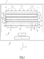
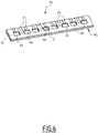
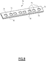
- FIG. 1-8 A preferred embodiment of at least one of the millimeter-wave antennas 1 is illustrated in Figures 1-8 .
- the antenna 1 comprises a containment casing, schematically illustrated in Figure 1 by the reference numeral 2, which houses inside it all or at least part of the components of the antenna.
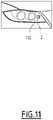
- This containment casing 2 is for example made of plastic material and is conveniently mounted integrated on the reflector of a corresponding front headlight or headlight assembly, or rear taillight or taillight assembly of the vehicle 100, for example as illustrated in Figure 11 for the right front headlight assembly 102.
- the antenna 1 may be substantially integrated into the structure of the associated head/taillight assembly, with its own containment casing 2 which is inserted in a suitable housing formed in the body of the reflector of the associated head/taillight or head/taillight assembly 101, 102, 103 and 104, in a manner such that its external surface, which faces the environment external to the vehicle 100, is substantially coplanar with the surface of the reflector itself.
- the antenna 1 can be substantially integrated into the structure of the associated side bumper 109, with its own containment casing 2 which is inserted in a suitable housing formed in the body of the bumper, for example in a manner such that its external surface, which faces the environment external to the vehicle 100, is substantially coplanar with the external surface of the side bumper itself.
- the four antennas 1 are connected, for the purposes and functionalities that will be described in detail below, to a first control unit 210 that is installed on the vehicle in a remote position distant from the antennas 1, and is connected to the antennas 1 by means of corresponding connection cables 211 which may be coaxial or digital type cables depending on the applications.
- each antenna 1 comprises, arranged inside the casing 2:
- the RF front-end module 3 has been represented as a separate module that is connected to the multilayer structure 5.
- the RF front-end module 3 could be connected to the multilayer structure in this configuration, or it could be integrated therewith, in the form of further additional layers and/or by using some of the layers of the multilayer structure 5 described below, such as for example one or more of the layers 40, 60, 70 and 80.
- the multilayer structure 5 comprises a plurality of layers stacked vertically along the reference direction indicated in Figure 1 by the reference axis X, the said multilayer structure including at least:
- the upper outer layer 10 comprises at least a first dielectric sublayer 12, for example made from ROGERS RO4350B material, and a plurality of first radiating elements 14 suitable for being fed with and radiating the signals to be transmitted.
- the first radiating elements 14 are made of electrically conductive material, for example copper, and are arranged spaced apart from each other on the first dielectric sublayer 12 substantially aligned in sequence along a reference horizontal axis Y that is perpendicular to the axis X.
- the first radiating elements 14 are preferably substantially identical to each other and each have a radiating area or surface "A1" measured in a plane transverse to the axis X, that is to say in the plane of the layer itself. For simplicity of illustration, this radiating area is clearly indicated in Figure 2 with oblique lines only for one radiating element 14.
- the first radiating elements 14 are of the type more precisely referred to as "patches", according to the nationally and internationally used term, with each having a substantially regular geometrical configuration, for example square or rectangular or circular.
- the upper outer layer 10 has a second sublayer 18, also referred to hereinafter as the first bonding sublayer 18, for example made from ROGERS RO4450 material, which is capable of enabling bonding of the upper outer layer 10 in its entirety with the layer of the plurality of layers immediately there-below.
- This first bonding sublayer 18 has a first thickness S1.
- the multilayer structure of the antenna 1 usefully comprises another inner layer 15, illustrated in Figure 3 , which is bonded to the first bonding sublayer 18, and is therefore interposed between the upper outer layer 10 and the first inner layer 20.
- the first inner layer 20 may be arranged immediately below and directly bonded in its upper part to the first bonding sublayer 18; in this case the further layer 15 is not used.
- the first inner layer 20 comprises at least an own first sublayer of conductive material 22, constituted for example of a copper foil, which is arranged on an own second sublayer of dielectric material 26.
- This second sublayer of dielectric material 26 may be prepared in a manner such as to have adhesive properties and enable bonding with the layer of the plurality of layers immediately there-below, that is to say in the illustrated exemplary embodiment with the second inner layer 30, or it may be combined with some adhesive material added so as to enable it to adhere to the subsequent layer.
- the first inner layer 20 comprises a plurality of through slots 24, having for example a U or C shaped form, which pass through the first sublayer of conductive material 22 and the second sublayer of dielectric material 26 and are suitable for conveying, towards at least the plurality of first radiating elements 14, the feeding signals to be radiated originating from the lower layers of the antenna 1 which will be described below.
- each through slot 24 is provided on the first inner layer 20 in an underlying position corresponding to the position of the associated first radiating element 14 on the upper outer layer 10.
- each slot 24 extends over the upper horizontal surface of the first inner layer 20 in a manner such that at least one end portion thereof is outside a virtual area obtained by projecting vertically (along the direction of the axis X) onto the first inner layer 20 itself the radiating surface "A1" of the associated first radiating element 14 or alternatively by projecting, again vertically, each slot 24 onto the first inner layer 20.
- each first radiating element 14 there is provided an associated pair of through slots 24, the two through slots 24 of each pair being formed on the first inner layer 20 in an underlying position corresponding to the position on the upper outer layer 10 of the associated first radiating element 14.
- the two slots of each pair of through slots 24, having for example a C or U shaped form, are arranged substantially perpendicular to each other.
- each slot 24 extends over the upper horizontal surface of the first inner layer 20 in a manner such that at least one end portion thereof extends outside a virtual area obtained by projecting vertically onto the first inner layer 20 itself the radiating surface "A1" of the associated first radiating element 14 (or alternatively by projecting, again vertically, each slot 24 onto the first inner layer 20).
- a plurality of metallised holes 29 passing through the sublayers 22 and 26 is defined.
- the second inner layer 30, which is attached above the sublayer 26, comprises at least an own first dielectric sublayer 32 (also referred to as third dielectric sublayer 32 to better distinguish it from the dielectric layers described previously) on which there is arranged a plurality of conductive lines 34, constituted for example of copper strips, that are suitable for conducting the feeding signals to be radiated at least towards the plurality of first radiating elements 14.
- an own first dielectric sublayer 32 also referred to as third dielectric sublayer 32 to better distinguish it from the dielectric layers described previously
- conductive lines 34 constituted for example of copper strips
- At least one corresponding conductive line 34 is associated with each radiating element.
- the third dielectric sublayer 32 acts as a bonding layer and therefore has adhesive properties or includes adhesive material in order to enable bonding with the layer of the plurality of layers immediately below the inner layer 30, that is to say in the exemplary embodiment illustrated with the further layer 40.
- the third dielectric sublayer 32 which may be made of or comprise for example ROGER RO4450 material, has an overall thickness S2 equal to or greater than the thickness S1 of the first bonding layer 18; in this manner, an improvement in the adapting or "matching" of the signals is advantageously obtained.
- the plurality of conductive lines 34 comprises for each first radiating element 14 a corresponding pair of conductive lines 34 associated therewith, and having for example shapes that differ from each other.
- each pair of conductive lines 34 comprises a first conductive line 34a, formed for example by a copper strip having a substantially rectilinear development, that is capable of transmitting to the corresponding first radiating element 14 the feeding signals to be radiated in a first direction of polarisation, and a second conductive line 34b, for example formed by an L-shaped copper strip, that is capable of transmitting to said corresponding first radiating element 14, the feeding signals to be radiated in a second direction of polarisation which is different from the first direction.
- These directions may coincide for example with the direction along the reference axis Z and the direction along the reference axis Y, illustrated in Figure 5 .
- the third inner layer 30 comprises metallised holes 29 that pass through its sublayers 34 and 32 and are vertically aligned each with a corresponding metallised through hole 29 formed on the first inner layer 20.
- each conductive line 34 extends over the plane of the sublayer 32 with the metallised holes 29 being arranged along both the edges of an associated conductive line 34 and replicating the path of the line itself.
- the conductive lines 34a and 34b of adjacent pairs of lines 34 are arranged in a mutually inverted sequence relative to each other. Furthermore, each line may be flipped to mirror-image or by 180° in the plane of the layer 30 itself, relative to the analogous preceding line.
- the inner layer 30 there is arranged: firstly, the first strip 34a that is capable of transmitting to the associated first radiating element 14 the feeding signals to be radiated in the first direction of polarisation; and then successively, the second conductive line 34b that is capable of transmitting to the same first radiating element 14 the feeding signals to be radiated in the second direction of polarisation.
- the second conductive strip 34b that is capable of transmitting to this subsequent radiating element 14 the feeding signals to be radiated in the second direction of polarisation, which is arranged with the L-shaped form flipped by 180° in the plane of the layer 30 relative to the analogous second line 34b of the preceding pair of lines; then, there is arranged the first line 34a (again flipped to mirror-image or by 180° relative to the analogous first line 34a of the preceding pair) that is capable of transmitting to the same subsequent radiating element 14 the feeding signals to be radiated in the first direction of polarisation.
- the inversion of the positioning order between the first strip 34a and the second strip 34b, with any relevant flipping relative to the analogous lines of the preceding pair, is regularly repeated at each subsequent radiating element 14 relative to the preceding one.
- one or more of the conductive lines 34 comprise each at least one section of line derived in parallel along the corresponding conductive line 34, preferably arranged to be coincident with the transition zone which in the exemplary embodiment happens to be close to the outer edge of the layer, but which in general could be found within a wider layer, and in particular to be coincident with a transition of a radiofrequency signal, capable of shifting the signal itself onto a different layer of the antenna, without introducing significant losses.
- This derived section makes it possible to artificially introduce alterations that serve to further enhance the so-called "matching" of the signal transition zones.
- This derived section of line may be constituted, for example, by a further portion of strip, and is illustrated in Figure 5 by the reference numeral 34c only for one pair of conductive lines 34 for the sake of simplicity of description.
- the further layer 40 which is arranged below and is adjacent to the second inner layer 30, comprises at least an own first sublayer of conductive material 42 (hereinafter also referred to as second conductive sublayer 42 so as to distinguish it from the preceding sublayer 22), constituted for example of a copper foil, which is arranged on an own second dielectric sublayer 46 (hereinafter also referred to as fourth dielectric sublayer 46 so as to distinguish it from the previously described dielectric layers).
- second conductive sublayer 42 so as to distinguish it from the preceding sublayer 22
- fourth dielectric sublayer 46 so as to distinguish it from the previously described dielectric layers
- the fourth dielectric sublayer 46 as well may be made directly from a material having adhesive properties or be combined with added adhesive material.
- the further layer 40 has defined thereon a plurality of first through openings 44 passing through its sublayers 42 and 46.
- each of said first through openings 44 is formed on the layer 40, and in particular on the sublayer of conductive material 42, in a position corresponding to the position of at least one associated through slot 24 of the plurality of through slots 24 defined on the first sublayer of conductive material 22 of the first inner layer 20.
- each first through opening 44 delimits an area of through-passage "B", measured transversely relative to the reference axis X, which is substantially equal to at least ⁇ 2 /4, that is to say at least a quarter of the square of the wavelength A measured in the dielectric material formed by the entire assembly of the third dielectric sublayer 32 immediately above the sublayer of conductive material 42 and the fourth dielectric sublayer 46 immediately below the sublayer of conductive material 42.
- the further layer 40 comprises metallised holes 29 which pass through at least its sublayer 42 and are arranged on parallel rows that are each aligned with a corresponding metallised through hole 29 formed on the first inner layer 20 and on the second inner layer 30.
- the multilayer structure of the antenna 1 according to the invention usefully includes at least one further inner layer, denoted in Figures 1 and 2 by the reference numeral 15 which is interposed between the upper outer layer 10 and the first inner layer 20, and is in particular bonded to the first bonding layer 18 there-above.
- the inner layer 15 comprises at least an own dielectric sublayer 17, hereinafter also referred to as a further dielectric sublayer 17, which is also made for example from ROGERS RO4350B material, and a plurality of second radiating elements 16 arranged spaced apart from each other and suitable for being fed with and radiating the signals to be transmitted.
- a further dielectric sublayer 17 which is also made for example from ROGERS RO4350B material
- second radiating elements 16 arranged spaced apart from each other and suitable for being fed with and radiating the signals to be transmitted.
- the inner layer 15 also comprises a further bonding sublayer 19, for example made from ROGERS RO4450 material, which is capable of enabling the bonding of the inner layer 15 to the underlying first inner layer 20.
- a further bonding sublayer 19 for example made from ROGERS RO4450 material, which is capable of enabling the bonding of the inner layer 15 to the underlying first inner layer 20.
- the second radiating elements 16 are made of electrically conductive material, for example copper, and are arranged spaced apart from each other on the further dielectric sublayer 17, substantially aligned along the reference axis Y.
- each second radiating element 16 is placed below and substantially aligned, at a certain distance, with a corresponding first radiating element 14.
- each second radiating element 16 there is at least one conductive line 34, in particular at least the same conductive line 34 that is associated with the corresponding first radiating element 14 positioned there-above.
- each radiating element 16 is associated with a pair of conductive lines 34a and 34b; as a consequence thereof, each pair of conductive lines 34 is associated both with a corresponding second radiating element 16 as well as with the first radiating element 14 arranged above said corresponding second radiating element 16.
- the second radiating elements 16 are preferably substantially identical to each other and each extend over a radiating area or surface "A2" (for simplicity of illustration clearly indicated in Figure 1 with oblique lines only for one radiating element 16) and in the illustrated embodiment they are also of the so-called "patch" type.
- each second radiating element 16 has a geometric configuration that is substantially regular, for example square, rectangular or circular.
- the second radiating elements 16 have each a respective radiation area A2, the latter also measured on a plane transverse to the axis X, that is at most equal to or preferably less than the radiation area A1 of each of the first radiating elements 14.
- the presence of the further layer 15 provided with the second radiating elements 16 makes it possible to appropriately widen the range of operating frequencies of the antenna 1 according to the invention.
- each slot 24 extends over the upper horizontal surface of the first inner layer 20 in a manner such that at least one end portion thereof is outside a virtual area obtained by projecting vertically onto the further inner layer 15 itself the radiating surface "A2" of the associated second radiating element 16 (or alternatively by projecting, again vertically, each slot 24 onto the further inner layer 15).
- each slot 24 is represented only in Figure 3 in broken line obtained by virtually projecting the slots 24 onto the layer 15.
- an analogous configuration occurs in respect of at least one end portion of the slots 24 spilling out of the radiation areas A1 of the first radiating elements 14, even if this illustration has not been replicated in Figure 2 for simplicity.
- the multilayer structure of the antenna 1 may include one or more further layers.
- first additional layer 60 hereinafter indicated as the third inner layer 60
- second additional layer 70 hereinafter indicated as the fourth inner layer 70
- third additional layer 80 hereinafter indicated as the lower outer layer 80
- the antenna 1 in the antenna 1 according to the invention, it is possible to use only one of such additional layers, only two, e.g. the first and second additional layers 60 and 70, or the first and third additional layers 60 and 80, or the second and third additional layers 70 and 80, or all of them as it will be described in the following according to the exemplary configuration depicted in figure 1 .
- the first additional or third inner layer 60 is arranged below and is adjacent to the further inner layer 40, for example bonded to the fourth dielectric sublayer 46.
- the third inner layer 60 comprises an own first sublayer of conductive material 62 (hereinafter also referred to as third conductive sublayer 62 so as to distinguish it from the preceding conductive sublayers 22 and 42) which is made for example from a copper foil in order to bring the feed voltages to the control chips of the antenna 1 and is arranged on an own second dielectric sublayer 66 (hereinafter also referred to as fifth dielectric sublayer 66 so as to distinguish it from the previously described dielectric layers) made from a material having adhesive properties or combined with some added adhesive material.
- an own first sublayer of conductive material 62 hereinafter also referred to as third conductive sublayer 62 so as to distinguish it from the preceding conductive sublayers 22 and 42
- an own second dielectric sublayer 66 hereinafter also referred to as fifth dielectric sublayer 66 so as to distinguish it from the previously described dielectric layers
- second through openings 64 which pass through the third conductive sublayer 62 and the fifth dielectric sublayer 66; these second through openings 64, in terms of number and shape thereof, are preferably substantially identical to the first through openings 44, with each of them being substantially aligned with a corresponding first through opening 44 relative to a substantially vertical reference direction defined by the axis X.
- a plurality of metallised through holes are also defined on the third inner layer and in particular only on the third conductive sublayer 62 , analogous to the through holes 29 indicated above, which are also arranged so as to be aligned each with a corresponding metallised through hole 29 formed on the first inner layer 20 and on the further inner layer 40.
- the through holes also pass through the dielectric layer 46 and, seen along the vertical direction defined by the reference axis X, when the structure of the antenna 1 is assembled, form a plurality of through channels that start from the first sublayer of conductive material 22 and terminate in the third sublayer of conductive material 62, as schematically illustrated in dashed line in Figure 1 .
- these channels formed by the vertically aligned through holes 29 may terminate at the second sublayer of conductive material 42.
- this first additional layer 60 it will constitute the lower outer layer of the antenna 1, i.e. the layer located at the lowest position of the stack of layers used.
- the fourth inner sublayer 70 is arranged below and is adjacent to the third inner layer 60, for example bonded to the fifth dielectric sublayer 66.
- the fourth inner layer 70 comprises at least an own first sublayer of conducting material 72 (hereinafter also referred to as fourth conducting sublayer 72 so as to distinguish it from the preceding conducting sublayers 22, 42 and 62), which is made for example from a copper foil that acts as a ground plane, and is arranged on an own second dielectric sublayer 76 (hereinafter also referred to as sixth dielectric sublayer 76 so as to distinguish it from the preceding dielectric sublayers) having adhesive properties.
- fourth conducting sublayer 72 so as to distinguish it from the preceding conducting sublayers 22, 42 and 62
- sixth dielectric sublayer 76 so as to distinguish it from the preceding dielectric sublayers
- these third through openings 74 are preferably substantially identical to the first through openings 44, with each of them being substantially aligned with a corresponding first through opening 44 relative to a substantially vertical reference direction defined by the axis X.
- the first through openings 44 are substantially aligned, along the vertical development of the multilayer structure, with the second through openings 64, and/or with the third through openings 74.
- first through openings 44, the second through openings 64, and the third through openings 74 are substantially aligned with each other along the vertical development of the multilayer structure.
- the second additional layer 70 will be arranged below and adjacent to the further inner layer 40 and it will constitute the lower outer layer of the antenna 1, i.e. the layer located at the lowest position of the stack of layers used.
- the second additional layer 70 will also constitute the lower outer layer of the antenna 1 if both the first and second additional layers 60 and 70 are used.
- the third additional layer or lower outer layer 80 is arranged below the fourth inner layer 70 and comprises one or more connection tracks, schematically illustrated in Figure 8 by dashed lines 82.
- connection tracks are for example constituted of copper traces arranged coincident with the face of the dielectric sublayer 76 opposite to that on which the conducting sublayer 72 is arranged.
- the connection tracks 82 are capable of being connected with one or more chips (not illustrated) for control and/or conditioning, for example for phase shifting or amplification, of the feeding signals to be radiated for at least the plurality of first radiating elements 14 and, where used, also for the second radiating elements 16.
- the third additional layer 80 will be arranged below and adjacent to the further inner layer 40, and if the second additional layer 70 is not used, the third additional layer will be arranged below and adjacent to the first additional layer 60.
- the third additional layer 80 is preferably meant to constitute the lower outer layer of the antenna 1.
- the antenna 1 further comprises at least one first series of parasitic radiating elements 11 and a second series of parasitic radiating elements 13 arranged on at least the said upper outer layer 10, in particular arranged on the first dielectric sublayer 14.
- the parasitic radiating elements 11 and 13 are arranged so as to be aligned along two rows that are parallel to each other with the plurality of first radiating elements 14 interposed between them.
- the series of parasitic radiating elements 11 and 13 serve to ameliorate the conformation of the irradiation beams of the transmitted signals.
- two further series of parasitic radiating elements may also be associated with the second radiating elements 16, where used; in this case, in a manner analogous to that which has been described above, these further parasitic radiating elements may be arranged on the sublayer of conductive material 17 along two parallel rows with the row of second radiating elements 16 interposed between them.
- the first control unit 210 of the system 200 is configured in a manner so as to select, in real time, at least one millimeter antenna 1 from among the four antennas 1 to which it is connected, from which the signals picked up at the input to the vehicle 100 are to be received, or to which signals to be radiated externally outside the vehicle 100 are to be transmitted, on the basis of one or more parameters indicative of the quality of the signal picked up at the input or transmitted at the output by each of the four millimeter antennas 1.
- the first control unit 210 is configured so as to select one single antenna 1 at a time, or to combine the signal received from multiple antennas 1 by means of digital or analogue methodologies, such as for example applying techniques including antenna array or diversity or MIMO ("Multiple Input - Multiple Output), of various types (amplitude and/or phase mixing of multiple signals performed in analogue or digital mode via Digital Signal Processing or DSP).
- digital or analogue methodologies such as for example applying techniques including antenna array or diversity or MIMO ("Multiple Input - Multiple Output), of various types (amplitude and/or phase mixing of multiple signals performed in analogue or digital mode via Digital Signal Processing or DSP).
- the selection of an antenna 1 is done by detecting the signal level (Received Signal Strength Indicator - RSSI) of each antenna 1 and choosing the antenna which provides the highest signal level (with the highest power).
- the first control unit 210 comprises a signal processor 212, such as for example a modem, connected to a control interface 214 for connecting the first control unit 210 to the various connection cables 211.
- a signal processor 212 such as for example a modem
- the control interface 4 of each antenna 1 comprises for example a frequency converter 4A and a control device 4B.
- the frequency converter 4A which is connected to the RF front-end module 3 and to the control device 4B, converts an input data signal at millimeter frequencies received by at least one of the radiating elements 14, 16 into a data signal at a first intermediate frequency for example between 1 GHz and 6 GHz (depending on the signal bandwidth) and converts an output data signal, originating from the signal processor 212 at the first intermediate frequency or at another frequency belonging to the same band of frequencies, into a data signal at millimeter frequencies in order to be transmitted by at least one radiating element 14, 16.
- control interface 214 of the first control unit 210 comprises a control device 216 which communicates with the control device 4B of each antenna 1, in order to conduct the control signals over the same coaxial cable 211 over which are transmitted the input and output data signals converted to the first intermediate frequency.
- control device 216 comprises for example an UP (type) frequency converter that is capable of converting the control signals to a second intermediate frequency that is different from the first intermediate frequency, for example comprised in the interval 0.1GHz and 1GHz.
- UP type
- the control device 216 comprises for example an UP (type) frequency converter that is capable of converting the control signals to a second intermediate frequency that is different from the first intermediate frequency, for example comprised in the interval 0.1GHz and 1GHz.
- the control device 216 of the control unit 210 further comprises one or more transceivers 226 for converting the control signals originating from the signal processor 212 into the second intermediate frequency.
- the control device 4B of the antenna 1 comprises for example a DOWN frequency converter that is capable of converting the control signals from the second intermediate frequency to a lower frequency in order to be able to control the frequency converter 4A and the RF front-end module 3.
- the control device 4B of each antenna 1 interprets the control signals and consequently acts on the associated frequency converter 4A and RF front-end module 3; to this end, the control device 4B comprises for example a transceiver (not shown in detail in the Figures) that converts the signals from the second intermediate frequency and a logic device, such as a microcontroller or an Application Specific Integrated Circuit (ASIC) or a Field Programmable Gate Array (FPGA) (also not shown in detail in the Figures).
- ASIC Application Specific Integrated Circuit
- FPGA Field Programmable Gate Array
- control unit 210 and each antenna 1 comprise respective power supply blocks (not illustrated in detail in the Figures) that communicate with each other through the respective coaxial connection cable 211.
- the control interface 214 comprises a plurality of DA/AD converter units 217, in which each DA/AD converter unit 217 is connected to a respective antenna 1 and comprises for example at least one analogue to digital converter (AD) and one digital to analogue converter (DA).
- AD analogue to digital converter
- DA digital to analogue converter
- the millimeter-wave data signal picked up at the input by at least one radiating element 14, 16 of an antenna 1 is amplified and routed over a correct path by the corresponding RF front-end module 3 towards the signal processor 212.
- the millimeter-wave data signal picked up at the input is sent to the frequency converter 4B which converts it to the first intermediate frequency in order to feed it onto the associated coaxial cable 211.
- This cable 211 transports it to one of the A/D converters of the converter unit 217 which digitizes the signal received and sends it to the signal processor 212.
- the signal processor 212 emits the output data signal in a digital format, and at least one DA converter of the unit of converters 217 converts it from digital to analogue at a first intermediate frequency.
- the output data signal at the first intermediate frequency is transmitted over at least one coaxial cable 211 and arrives at a frequency converter 4A of at least one antenna 1 which converts it to millimeter frequencies.
- the output data signal at millimeter frequency is amplified and routed by the respective front-end 3 to at least one radiating element 14, 16 which transmits it into the air.
- the control signals are generated by the signal processor 212 and are sent to the control device 216 which converts them to a second intermediate frequency and feeds them into one or more of the coaxial cables 211.
- the control signals at the second intermediate frequency then arrive at least at one control device 4B of an antenna 1 and are converted to a lower frequency suitable for controlling the associated frequency converter 4A and RF front-end module 3.
- the control interface 4 of each antenna 1 additionally also includes a DA/AD converter unit 4C comprising a digital/analogue (DA) converter and an analogue/digital (AD) converter designed to render the analogue signals suitable for digital transmission and vice versa.
- DA digital/analogue
- AD analogue/digital
- control device of each antenna 1 is for example capable of inserting into the flow of the input data signal also a signal for diagnosing its status.
- the control device 214 of the control unit 210 is capable of inserting into the flow of the output data signal also the control signals that serve to drive for each antenna the frequency converter 4A, the RF front-end module 3, and the DA/AD converter unit.
- the control device 4B of each antenna is capable of separating the output data signal from the control signals.
- the control device 214 of the unit 210 is capable of separating the input data signal from the diagnostics signal.
- control device 4B of each antenna 1 comprises digital transmission controllers, serialisers/deserialisers that are capable of encapsulating/decapsulating and digital signals and a computing unit (for example a microcontroller, ASIC or FPGA) for the management of the devices of the antennas 1, and the control device 214 of the control unit 210 comprises for example digital transmission controllers and serialisers/deserialisers that are capable of encapsulating/decapsulating digital signals.
- some poles of the digital cable 211 may be dedicated to the transport of DC power supply, thereby avoiding the need for ad hoc power supply blocks.
- an input data signal at millimeter frequency is picked up by at least one radiating element 14, 16 of an antenna 1 and sent to the corresponding RF front-end module 3 which amplifies and routes it.
- the input data signal is converted by the frequency converter 4A from the millimeter frequency to an intermediate frequency between for example 0.1 GHz and 6 GHz. Then the input data signal is digitised by an AD converter of the converter unit 4C.
- the control device 4B encapsulates the input data signal together with the diagnostics signal in a digital communication protocol, in a manner so as to obtain an encapsulated signal, and transmits it in digital format over the corresponding digital cable 211.
- the signal encapsulated in digital format then arrives at the control device 216 of the control unit 210 which decapsulates it in a manner so as to obtain the input data signal which is sent to the signal processor 212.
- the signal processor 212 emits the output data signal in a digital format.
- the control device 216 encapsulates the output data signal with the control signals in a manner so as to obtain an encapsulated signal which is transmitted over the digital cables 211.
- the encapsulated signal is received by the control device 4B of at least one antenna 1 and is decapsulated, in a manner so as to obtain the output data signal in digital format.
- the output data signal in digital format is sent to a DA converter of the converter unit 4C which converts it into analogue.
- the analogue output data signal is converted to a millimeter frequency by the frequency converter 4A.
- the output data signal at millimeter frequencies is amplified and routed by the corresponding RF front-end module 3 towards at least one of the radiating elements 14, 16 of the antenna 1 which transmits it into the air.
- the control signals are generated by the signal processor 212 in digital format and are sent to the control device 216 of the central control unit which encapsulates them together with the output data signal so as to obtain the encapsulated signal which is transmitted over one or more digital cables 211.
- the encapsulated signal (comprising the output data signal and the control signals) is received by the control device 4B of at least one antenna 1 which decapsulates the signal so as to obtain the digital control signals for controlling respectively the respective frequency converter 4A, the RF front-end module 3 and the DA/AD converter unit 4C.
- the antennas 1 can receive/transmit signals by means of their respective digital cables 211 that are connected to respective dedicated data buses, or it is possible to use a single shared data bus.
- the various signals that travel in the shared data bus have one address (shared band) and the identification of the correct sender/receiver takes place by means of the transmission protocol headers inserted by the respective control devices that encapsulate the signals to be sent over the shared data bus.
- the data transceiver system 200 installed on board the vehicle 100 additionally comprises also a second set of antennas 230 for transceiving of data in a frequency band lower than the operating band of the first set of millimeter-wave antennas 1.
- the data transceiver system 200 preferably comprises a second control unit 250 which is operatively associated with and is configured to control the operation of the second set of antennas 230.
- the data transceiver system 200 further comprises at least one further antenna 240 for transceiving of data in an intermediate frequency band between the operating frequency bands of said first and second sets of antennas 1, 230, and the second control unit 250 is also operatively associated with and is configured to control the operation of the at least one further antenna 240.
- the second control unit 250 is connected to the antennas 230 and/or 240, for example by means of respective cables 231.
- the second set of antennas 230 also comprises at least four antennas 230 which are each installed in a corresponding quadrant of said four quadrants A, B, C, D, and of which, a first and a second antennas 230 are installed at the front bumper 106 of the vehicle, for example in proximity to the respective headlights 101 and 102, and a third and a fourth antennas 230 are installed at the rear bumper 107, for example in proximity to the respective taillights 103 and 104.
- the four antennas 230 operate at a frequency lower than or equal to 5GHz.
- said at least one further antenna 240 may be installed on the roof 108 of the vehicle 100, for example within a cupole or shark fin antenna or it may also be installed internally inside the vehicle, for example in proximity to the internal rear-view mirror, or it is possible to use two antennas 240 contemporaneously.
- the or each antenna 240 operates at a frequency in the region of 5.9 GHz, and is dedicated to the transceiving of Vehicle-to-Everything (V2X) data.
- V2X Vehicle-to-Everything
- the antennas 230 and the or each further antenna 240 may be of a type that is commercially available in the market and for this reason they are not described in detail herein.
- the vehicle 100 according to the invention allows achieving the intended object since the data transceiver system 200 installed on board represents a good compromise between the number of antennas installed, in particular of the millimeter-wave type, and effectiveness of the data transmission/reception coverage around the vehicle 100, with optimized occupation of space and encumbrances. Furthermore, the structure of the antenna 1 described previously makes it possible to obtain a solution that combines transmission/reception efficiency with reduced overall dimensions and production costs. Clearly, where possible or required, it is possible to add to the optimized configuration described above, one or more further antennas.
- the four millimeter-wave antennas 1 were all installed to be coincident with the respective four head/taillights or head/taillight assemblies, it is possible to add one or more antennas 1 installed in the corresponding side bumpers 109, or vice versa, if the four antennas 1 were installed in the respective side bumpers 109, it is possible to add one or more antenna(s) 1 installed in the corresponding head/taillights or head/taillight assemblies.
Landscapes
- Engineering & Computer Science (AREA)
- Remote Sensing (AREA)
- Physics & Mathematics (AREA)
- Electromagnetism (AREA)
- Variable-Direction Aerials And Aerial Arrays (AREA)
- Circuits Of Receivers In General (AREA)
- Measuring Pulse, Heart Rate, Blood Pressure Or Blood Flow (AREA)
Applications Claiming Priority (1)
| Application Number | Priority Date | Filing Date | Title |
|---|---|---|---|
| IT102021000003866A IT202100003866A1 (it) | 2021-02-19 | 2021-02-19 | Veicolo con sistema ottimizzato per la ricetrasmissione di dati |
Publications (3)
| Publication Number | Publication Date |
|---|---|
| EP4047743A2 true EP4047743A2 (de) | 2022-08-24 |
| EP4047743A3 EP4047743A3 (de) | 2022-11-02 |
| EP4047743B1 EP4047743B1 (de) | 2025-02-26 |
Family
ID=75769831
Family Applications (1)
| Application Number | Title | Priority Date | Filing Date |
|---|---|---|---|
| EP22157411.4A Active EP4047743B1 (de) | 2021-02-19 | 2022-02-18 | Fahrzeug mit optimiertem system zum senden und empfangen von daten |
Country Status (2)
| Country | Link |
|---|---|
| EP (1) | EP4047743B1 (de) |
| IT (1) | IT202100003866A1 (de) |
Family Cites Families (5)
| Publication number | Priority date | Publication date | Assignee | Title |
|---|---|---|---|---|
| DE102004032015A1 (de) * | 2004-07-01 | 2006-01-26 | Siemens Ag | Schienenfahrzeug mit einer Überanstreckungsstrecke für Daten und/oder Befehle |
| DE102013021819A1 (de) * | 2013-12-21 | 2015-06-25 | Valeo Schalter Und Sensoren Gmbh | Radarvorrichtung mit einer Fahrzeugleuchte und einem Radarsensor sowie Kraftfahrzeug mit einer Radarvorrichtung |
| JP6528798B2 (ja) * | 2017-03-30 | 2019-06-12 | トヨタ自動車株式会社 | 車載ミリ波通信装置および通信方法 |
| KR102578394B1 (ko) * | 2018-12-10 | 2023-09-14 | 엘지전자 주식회사 | 차량에 탑재되는 안테나 시스템 |
| JP7520970B2 (ja) * | 2019-12-27 | 2024-07-23 | インテル コーポレイション | 無線通信及びレーダ用の組み込みアンテナ構造 |
-
2021
- 2021-02-19 IT IT102021000003866A patent/IT202100003866A1/it unknown
-
2022
- 2022-02-18 EP EP22157411.4A patent/EP4047743B1/de active Active
Also Published As
| Publication number | Publication date |
|---|---|
| IT202100003866A1 (it) | 2022-08-19 |
| EP4047743A3 (de) | 2022-11-02 |
| EP4047743B1 (de) | 2025-02-26 |
Similar Documents
| Publication | Publication Date | Title |
|---|---|---|
| KR102552305B1 (ko) | 차량에 배치되는 광대역 안테나 | |
| US20240297433A1 (en) | Antenna-on-package integrated circuit device | |
| US11791542B2 (en) | RF devices including conformal antennas and methods for manufacturing thereof | |
| US8786496B2 (en) | Three-dimensional array antenna on a substrate with enhanced backlobe suppression for mm-wave automotive applications | |
| US8022861B2 (en) | Dual-band antenna array and RF front-end for mm-wave imager and radar | |
| US11682824B2 (en) | Antenna module disposed in vehicle | |
| US11258161B2 (en) | Antenna-on-package integrated circuit device | |
| JPH08114667A (ja) | レーダーモジュール | |
| CN112868136A (zh) | 车辆用天线系统 | |
| US20200313287A1 (en) | Inverted microstrip travelling wave patch array antenna system | |
| US12438283B2 (en) | Antenna module arranged in vehicle | |
| CN102655266B (zh) | 多频带天线 | |
| US12431608B2 (en) | Antenna module arranged in vehicle | |
| US20260018778A1 (en) | Antenna module disposed in vehicle | |
| US20080316126A1 (en) | Antenna System for a Radar Transceiver | |
| KR102709419B1 (ko) | 차량에 배치되는 안테나 모듈 | |
| EP4047743B1 (de) | Fahrzeug mit optimiertem system zum senden und empfangen von daten | |
| KR20240070594A (ko) | 차량에 배치되는 광대역 안테나 | |
| US11923605B2 (en) | Millimeter-wave antenna for 5G applications and vehicle comprising such antenna | |
| US20240322448A1 (en) | Thin sheet-like antenna for narrowband vehicular communication | |
| US20240250437A1 (en) | Thin sheet-like antenna for narrowband vehicular communication | |
| EP4579950B1 (de) | In einem fahrzeug angeordnetes antennenmodul |
Legal Events
| Date | Code | Title | Description |
|---|---|---|---|
| PUAI | Public reference made under article 153(3) epc to a published international application that has entered the european phase |
Free format text: ORIGINAL CODE: 0009012 |
|
| STAA | Information on the status of an ep patent application or granted ep patent |
Free format text: STATUS: THE APPLICATION HAS BEEN PUBLISHED |
|
| AK | Designated contracting states |
Kind code of ref document: A2 Designated state(s): AL AT BE BG CH CY CZ DE DK EE ES FI FR GB GR HR HU IE IS IT LI LT LU LV MC MK MT NL NO PL PT RO RS SE SI SK SM TR |
|
| PUAL | Search report despatched |
Free format text: ORIGINAL CODE: 0009013 |
|
| AK | Designated contracting states |
Kind code of ref document: A3 Designated state(s): AL AT BE BG CH CY CZ DE DK EE ES FI FR GB GR HR HU IE IS IT LI LT LU LV MC MK MT NL NO PL PT RO RS SE SI SK SM TR |
|
| RIC1 | Information provided on ipc code assigned before grant |
Ipc: H01Q 5/30 20150101ALI20220923BHEP Ipc: H01Q 21/28 20060101ALI20220923BHEP Ipc: H01Q 21/20 20060101ALI20220923BHEP Ipc: H01Q 19/00 20060101ALI20220923BHEP Ipc: H01Q 21/06 20060101ALI20220923BHEP Ipc: H01Q 9/04 20060101ALI20220923BHEP Ipc: H01Q 1/32 20060101AFI20220923BHEP |
|
| STAA | Information on the status of an ep patent application or granted ep patent |
Free format text: STATUS: REQUEST FOR EXAMINATION WAS MADE |
|
| 17P | Request for examination filed |
Effective date: 20230331 |
|
| RBV | Designated contracting states (corrected) |
Designated state(s): AL AT BE BG CH CY CZ DE DK EE ES FI FR GB GR HR HU IE IS IT LI LT LU LV MC MK MT NL NO PL PT RO RS SE SI SK SM TR |
|
| GRAP | Despatch of communication of intention to grant a patent |
Free format text: ORIGINAL CODE: EPIDOSNIGR1 |
|
| STAA | Information on the status of an ep patent application or granted ep patent |
Free format text: STATUS: GRANT OF PATENT IS INTENDED |
|
| INTG | Intention to grant announced |
Effective date: 20241120 |
|
| GRAS | Grant fee paid |
Free format text: ORIGINAL CODE: EPIDOSNIGR3 |
|
| GRAA | (expected) grant |
Free format text: ORIGINAL CODE: 0009210 |
|
| STAA | Information on the status of an ep patent application or granted ep patent |
Free format text: STATUS: THE PATENT HAS BEEN GRANTED |
|
| AK | Designated contracting states |
Kind code of ref document: B1 Designated state(s): AL AT BE BG CH CY CZ DE DK EE ES FI FR GB GR HR HU IE IS IT LI LT LU LV MC MK MT NL NO PL PT RO RS SE SI SK SM TR |
|
| REG | Reference to a national code |
Ref country code: GB Ref legal event code: FG4D |
|
| REG | Reference to a national code |
Ref country code: CH Ref legal event code: EP |
|
| REG | Reference to a national code |
Ref country code: DE Ref legal event code: R096 Ref document number: 602022010966 Country of ref document: DE |
|
| REG | Reference to a national code |
Ref country code: IE Ref legal event code: FG4D |
|
| REG | Reference to a national code |
Ref country code: NL Ref legal event code: MP Effective date: 20250226 |
|
| PG25 | Lapsed in a contracting state [announced via postgrant information from national office to epo] |
Ref country code: RS Free format text: LAPSE BECAUSE OF FAILURE TO SUBMIT A TRANSLATION OF THE DESCRIPTION OR TO PAY THE FEE WITHIN THE PRESCRIBED TIME-LIMIT Effective date: 20250526 |
|
| PG25 | Lapsed in a contracting state [announced via postgrant information from national office to epo] |
Ref country code: FI Free format text: LAPSE BECAUSE OF FAILURE TO SUBMIT A TRANSLATION OF THE DESCRIPTION OR TO PAY THE FEE WITHIN THE PRESCRIBED TIME-LIMIT Effective date: 20250226 |
|
| PG25 | Lapsed in a contracting state [announced via postgrant information from national office to epo] |
Ref country code: PL Free format text: LAPSE BECAUSE OF FAILURE TO SUBMIT A TRANSLATION OF THE DESCRIPTION OR TO PAY THE FEE WITHIN THE PRESCRIBED TIME-LIMIT Effective date: 20250226 |
|
| PG25 | Lapsed in a contracting state [announced via postgrant information from national office to epo] |
Ref country code: ES Free format text: LAPSE BECAUSE OF FAILURE TO SUBMIT A TRANSLATION OF THE DESCRIPTION OR TO PAY THE FEE WITHIN THE PRESCRIBED TIME-LIMIT Effective date: 20250226 |
|
| REG | Reference to a national code |
Ref country code: LT Ref legal event code: MG9D |
|
| PG25 | Lapsed in a contracting state [announced via postgrant information from national office to epo] |
Ref country code: NO Free format text: LAPSE BECAUSE OF FAILURE TO SUBMIT A TRANSLATION OF THE DESCRIPTION OR TO PAY THE FEE WITHIN THE PRESCRIBED TIME-LIMIT Effective date: 20250526 Ref country code: IS Free format text: LAPSE BECAUSE OF FAILURE TO SUBMIT A TRANSLATION OF THE DESCRIPTION OR TO PAY THE FEE WITHIN THE PRESCRIBED TIME-LIMIT Effective date: 20250626 |
|
| PG25 | Lapsed in a contracting state [announced via postgrant information from national office to epo] |
Ref country code: NL Free format text: LAPSE BECAUSE OF FAILURE TO SUBMIT A TRANSLATION OF THE DESCRIPTION OR TO PAY THE FEE WITHIN THE PRESCRIBED TIME-LIMIT Effective date: 20250226 |
|
| PG25 | Lapsed in a contracting state [announced via postgrant information from national office to epo] |
Ref country code: HR Free format text: LAPSE BECAUSE OF FAILURE TO SUBMIT A TRANSLATION OF THE DESCRIPTION OR TO PAY THE FEE WITHIN THE PRESCRIBED TIME-LIMIT Effective date: 20250226 |
|
| PG25 | Lapsed in a contracting state [announced via postgrant information from national office to epo] |
Ref country code: PT Free format text: LAPSE BECAUSE OF FAILURE TO SUBMIT A TRANSLATION OF THE DESCRIPTION OR TO PAY THE FEE WITHIN THE PRESCRIBED TIME-LIMIT Effective date: 20250626 Ref country code: LV Free format text: LAPSE BECAUSE OF FAILURE TO SUBMIT A TRANSLATION OF THE DESCRIPTION OR TO PAY THE FEE WITHIN THE PRESCRIBED TIME-LIMIT Effective date: 20250226 |
|
| PG25 | Lapsed in a contracting state [announced via postgrant information from national office to epo] |
Ref country code: BG Free format text: LAPSE BECAUSE OF FAILURE TO SUBMIT A TRANSLATION OF THE DESCRIPTION OR TO PAY THE FEE WITHIN THE PRESCRIBED TIME-LIMIT Effective date: 20250226 Ref country code: GR Free format text: LAPSE BECAUSE OF FAILURE TO SUBMIT A TRANSLATION OF THE DESCRIPTION OR TO PAY THE FEE WITHIN THE PRESCRIBED TIME-LIMIT Effective date: 20250527 |
|
| REG | Reference to a national code |
Ref country code: AT Ref legal event code: MK05 Ref document number: 1771613 Country of ref document: AT Kind code of ref document: T Effective date: 20250226 |
|
| PG25 | Lapsed in a contracting state [announced via postgrant information from national office to epo] |
Ref country code: SE Free format text: LAPSE BECAUSE OF FAILURE TO SUBMIT A TRANSLATION OF THE DESCRIPTION OR TO PAY THE FEE WITHIN THE PRESCRIBED TIME-LIMIT Effective date: 20250226 |
|
| PG25 | Lapsed in a contracting state [announced via postgrant information from national office to epo] |
Ref country code: SM Free format text: LAPSE BECAUSE OF FAILURE TO SUBMIT A TRANSLATION OF THE DESCRIPTION OR TO PAY THE FEE WITHIN THE PRESCRIBED TIME-LIMIT Effective date: 20250226 |
|
| PG25 | Lapsed in a contracting state [announced via postgrant information from national office to epo] |
Ref country code: DK Free format text: LAPSE BECAUSE OF FAILURE TO SUBMIT A TRANSLATION OF THE DESCRIPTION OR TO PAY THE FEE WITHIN THE PRESCRIBED TIME-LIMIT Effective date: 20250226 |
|
| PG25 | Lapsed in a contracting state [announced via postgrant information from national office to epo] |
Ref country code: IT Free format text: LAPSE BECAUSE OF FAILURE TO SUBMIT A TRANSLATION OF THE DESCRIPTION OR TO PAY THE FEE WITHIN THE PRESCRIBED TIME-LIMIT Effective date: 20250226 |
|
| RAP4 | Party data changed (patent owner data changed or rights of a patent transferred) |
Owner name: ASK INDUSTRIES S.P.A. |
|
| PG25 | Lapsed in a contracting state [announced via postgrant information from national office to epo] |
Ref country code: AT Free format text: LAPSE BECAUSE OF FAILURE TO SUBMIT A TRANSLATION OF THE DESCRIPTION OR TO PAY THE FEE WITHIN THE PRESCRIBED TIME-LIMIT Effective date: 20250226 |
|
| PG25 | Lapsed in a contracting state [announced via postgrant information from national office to epo] |
Ref country code: EE Free format text: LAPSE BECAUSE OF FAILURE TO SUBMIT A TRANSLATION OF THE DESCRIPTION OR TO PAY THE FEE WITHIN THE PRESCRIBED TIME-LIMIT Effective date: 20250226 Ref country code: CZ Free format text: LAPSE BECAUSE OF FAILURE TO SUBMIT A TRANSLATION OF THE DESCRIPTION OR TO PAY THE FEE WITHIN THE PRESCRIBED TIME-LIMIT Effective date: 20250226 |
|
| PG25 | Lapsed in a contracting state [announced via postgrant information from national office to epo] |
Ref country code: RO Free format text: LAPSE BECAUSE OF FAILURE TO SUBMIT A TRANSLATION OF THE DESCRIPTION OR TO PAY THE FEE WITHIN THE PRESCRIBED TIME-LIMIT Effective date: 20250226 |
|
| PG25 | Lapsed in a contracting state [announced via postgrant information from national office to epo] |
Ref country code: SK Free format text: LAPSE BECAUSE OF FAILURE TO SUBMIT A TRANSLATION OF THE DESCRIPTION OR TO PAY THE FEE WITHIN THE PRESCRIBED TIME-LIMIT Effective date: 20250226 |
|
| P01 | Opt-out of the competence of the unified patent court (upc) registered |
Free format text: CASE NUMBER: UPC_APP_7501_4047743/2025 Effective date: 20250918 |
|
| REG | Reference to a national code |
Ref country code: DE Ref legal event code: R097 Ref document number: 602022010966 Country of ref document: DE |
|
| PLBE | No opposition filed within time limit |
Free format text: ORIGINAL CODE: 0009261 |
|
| STAA | Information on the status of an ep patent application or granted ep patent |
Free format text: STATUS: NO OPPOSITION FILED WITHIN TIME LIMIT |
|
| 26N | No opposition filed |
Effective date: 20251127 |
|
| PGFP | Annual fee paid to national office [announced via postgrant information from national office to epo] |
Ref country code: GB Payment date: 20260223 Year of fee payment: 5 |
|
| PGFP | Annual fee paid to national office [announced via postgrant information from national office to epo] |
Ref country code: DE Payment date: 20260227 Year of fee payment: 5 |
|
| PGFP | Annual fee paid to national office [announced via postgrant information from national office to epo] |
Ref country code: FR Payment date: 20260225 Year of fee payment: 5 |