EP4044164A1 - Gate driving circuit and display device - Google Patents
Gate driving circuit and display device Download PDFInfo
- Publication number
- EP4044164A1 EP4044164A1 EP21760337.2A EP21760337A EP4044164A1 EP 4044164 A1 EP4044164 A1 EP 4044164A1 EP 21760337 A EP21760337 A EP 21760337A EP 4044164 A1 EP4044164 A1 EP 4044164A1
- Authority
- EP
- European Patent Office
- Prior art keywords
- electrically connected
- switching transistor
- signal terminal
- gate
- electrode
- Prior art date
- Legal status (The legal status is an assumption and is not a legal conclusion. Google has not performed a legal analysis and makes no representation as to the accuracy of the status listed.)
- Pending
Links
Images


Classifications
-
- G—PHYSICS
- G09—EDUCATION; CRYPTOGRAPHY; DISPLAY; ADVERTISING; SEALS
- G09G—ARRANGEMENTS OR CIRCUITS FOR CONTROL OF INDICATING DEVICES USING STATIC MEANS TO PRESENT VARIABLE INFORMATION
- G09G3/00—Control arrangements or circuits, of interest only in connection with visual indicators other than cathode-ray tubes
- G09G3/20—Control arrangements or circuits, of interest only in connection with visual indicators other than cathode-ray tubes for presentation of an assembly of a number of characters, e.g. a page, by composing the assembly by combination of individual elements arranged in a matrix no fixed position being assigned to or needed to be assigned to the individual characters or partial characters
-
- G—PHYSICS
- G09—EDUCATION; CRYPTOGRAPHY; DISPLAY; ADVERTISING; SEALS
- G09G—ARRANGEMENTS OR CIRCUITS FOR CONTROL OF INDICATING DEVICES USING STATIC MEANS TO PRESENT VARIABLE INFORMATION
- G09G3/00—Control arrangements or circuits, of interest only in connection with visual indicators other than cathode-ray tubes
- G09G3/20—Control arrangements or circuits, of interest only in connection with visual indicators other than cathode-ray tubes for presentation of an assembly of a number of characters, e.g. a page, by composing the assembly by combination of individual elements arranged in a matrix no fixed position being assigned to or needed to be assigned to the individual characters or partial characters
- G09G3/22—Control arrangements or circuits, of interest only in connection with visual indicators other than cathode-ray tubes for presentation of an assembly of a number of characters, e.g. a page, by composing the assembly by combination of individual elements arranged in a matrix no fixed position being assigned to or needed to be assigned to the individual characters or partial characters using controlled light sources
- G09G3/30—Control arrangements or circuits, of interest only in connection with visual indicators other than cathode-ray tubes for presentation of an assembly of a number of characters, e.g. a page, by composing the assembly by combination of individual elements arranged in a matrix no fixed position being assigned to or needed to be assigned to the individual characters or partial characters using controlled light sources using electroluminescent panels
- G09G3/32—Control arrangements or circuits, of interest only in connection with visual indicators other than cathode-ray tubes for presentation of an assembly of a number of characters, e.g. a page, by composing the assembly by combination of individual elements arranged in a matrix no fixed position being assigned to or needed to be assigned to the individual characters or partial characters using controlled light sources using electroluminescent panels semiconductive, e.g. using light-emitting diodes [LED]
- G09G3/3208—Control arrangements or circuits, of interest only in connection with visual indicators other than cathode-ray tubes for presentation of an assembly of a number of characters, e.g. a page, by composing the assembly by combination of individual elements arranged in a matrix no fixed position being assigned to or needed to be assigned to the individual characters or partial characters using controlled light sources using electroluminescent panels semiconductive, e.g. using light-emitting diodes [LED] organic, e.g. using organic light-emitting diodes [OLED]
- G09G3/3266—Details of drivers for scan electrodes
-
- G—PHYSICS
- G09—EDUCATION; CRYPTOGRAPHY; DISPLAY; ADVERTISING; SEALS
- G09G—ARRANGEMENTS OR CIRCUITS FOR CONTROL OF INDICATING DEVICES USING STATIC MEANS TO PRESENT VARIABLE INFORMATION
- G09G3/00—Control arrangements or circuits, of interest only in connection with visual indicators other than cathode-ray tubes
- G09G3/20—Control arrangements or circuits, of interest only in connection with visual indicators other than cathode-ray tubes for presentation of an assembly of a number of characters, e.g. a page, by composing the assembly by combination of individual elements arranged in a matrix no fixed position being assigned to or needed to be assigned to the individual characters or partial characters
- G09G3/34—Control arrangements or circuits, of interest only in connection with visual indicators other than cathode-ray tubes for presentation of an assembly of a number of characters, e.g. a page, by composing the assembly by combination of individual elements arranged in a matrix no fixed position being assigned to or needed to be assigned to the individual characters or partial characters by control of light from an independent source
- G09G3/36—Control arrangements or circuits, of interest only in connection with visual indicators other than cathode-ray tubes for presentation of an assembly of a number of characters, e.g. a page, by composing the assembly by combination of individual elements arranged in a matrix no fixed position being assigned to or needed to be assigned to the individual characters or partial characters by control of light from an independent source using liquid crystals
- G09G3/3611—Control of matrices with row and column drivers
- G09G3/3674—Details of drivers for scan electrodes
-
- G—PHYSICS
- G11—INFORMATION STORAGE
- G11C—STATIC STORES
- G11C19/00—Digital stores in which the information is moved stepwise, e.g. shift registers
- G11C19/28—Digital stores in which the information is moved stepwise, e.g. shift registers using semiconductor elements
-
- G—PHYSICS
- G09—EDUCATION; CRYPTOGRAPHY; DISPLAY; ADVERTISING; SEALS
- G09G—ARRANGEMENTS OR CIRCUITS FOR CONTROL OF INDICATING DEVICES USING STATIC MEANS TO PRESENT VARIABLE INFORMATION
- G09G2310/00—Command of the display device
- G09G2310/02—Addressing, scanning or driving the display screen or processing steps related thereto
- G09G2310/0264—Details of driving circuits
- G09G2310/0286—Details of a shift registers arranged for use in a driving circuit
Definitions
- the disclosure relates to the technical field of display, in particular to a gate driving circuit and a display device.
- a GOA gate driver on array
- TFT thin film transistor
- IC gate integrated circuit
- An embodiment of the disclosure provides a gate driving circuit, including a plurality of cascaded shift registers, wherein each shift register includes an input signal terminal, a reset signal terminal, an output control terminal and a gate signal output terminal; the gate signal output terminals are electrically connected to gate lines of a display panel in a one-to-one corresponding mode; in every five adjacent shift registers, an output control terminal of a first shift register among the every five adjacent shift registers is electrically connected to an input signal terminal of a fifth shift register among the every five adjacent shift registers; and in every six adjacent shift registers, an output control terminal of a sixth shift register among the every six adjacent shift registers is electrically connected to the reset signal terminal of the first shift register among the every six adjacent shift registers.
- the gate driving circuit provided by the embodiment of the disclosure includes 10 clock signal lines, wherein each shift register further includes a clock signal terminal; the clock signal terminal of the (10k-9)th shift register is electrically connected to the first clock signal line, the clock signal terminal of the (10k-8)th shift register is electrically connected to the second clock signal line, the clock signal terminal of the (10k-7)th shift register is electrically connected to the third clock signal line, the clock signal terminal of the (10k-6)th shift register is electrically connected to the fourth clock signal line, the clock signal terminal of the (10k-5)th shift register is electrically connected to the fifth clock signal line, the clock signal terminal of the (10k-4)th shift register is electrically connected to the sixth clock signal line, the clock signal terminal of the (10k-3)th shift register is electrically connected to the seventh clock signal line, the clock signal terminal of the (10k-2)th shift register is electrically connected to the eighth clock signal line, the clock signal terminal of the (10k-1)th shift register is electrically connected to the ninth clock signal line, and the clock
- a clock signal duty cycle of each clock signal line is approximately 40%.
- each shift register includes: an input circuit, a reset circuit, a control circuit, a first output circuit, a second output circuit and a resetting circuit.
- the input circuit is configured to control a potential of a first node in response to a signal input by the input signal terminal;
- the reset circuit is configured to provide a signal input by a first reference signal terminal to the first node in response to a signal input by the reset signal terminal;
- the control circuit is configured to provide the signal of the first reference signal terminal to a second node in response to the signal input by the input signal terminal, control the potentials of the first node and the second node in response to a signal input by a control signal terminal, provide a signal of a second reference signal terminal to the gate signal output terminal in response to a potential of the second node, and provide the signal of the first reference signal terminal to the output control terminal in response to the potential of the second node;
- the first output circuit is configured to provide a signal of the clock signal terminal to the
- the input circuit includes a first switching transistor; and a gate and a first electrode of the first switching transistor are electrically connected to the input signal terminal, and a second electrode of the first switching transistor is electrically connected to the first node.
- the reset circuit includes: a second switching transistor; and a gate of the second switching transistor is electrically connected to the reset signal terminal, a first electrode of the second switching transistor is electrically connected to the first node, and a second electrode of the second switching transistor is electrically connected to the first reference signal terminal.
- the control circuit includes: a third switching transistor, a fourth switching transistor, a fifth switching transistor, a sixth switching transistor, a seventh switching transistor, an eighth switching transistor, a ninth switching transistor and a tenth switching transistor.
- Agate of the third switching transistor is electrically connected to the input signal terminal, a first electrode of the third switching transistor is electrically connected to the second node, and a second electrode of the third switching transistor is electrically connected to the first reference signal terminal.
- a gate of the fourth switching transistor is electrically connected to the second node, a first electrode of the fourth switching transistor is electrically connected to the first node, and a second electrode of the fourth switching transistor is electrically connected to the first reference signal terminal.
- a gate of the fifth switching transistor is electrically connected to the second node, a first electrode of the fifth switching transistor is electrically connected to the gate signal output terminal, and a second electrode of the fifth switching transistor is electrically connected to the second reference signal terminal.
- a gate and a first electrode of the sixth switching transistor are electrically connected to the control signal terminal, and a second electrode of the sixth switching transistor is electrically connected to a first electrode of the eighth switching transistor and a gate of the seventh switching transistor respectively.
- a first electrode of the seventh switching transistor is electrically connected to the control signal terminal, and a second electrode of the seventh switching transistor is electrically connected to the second node.
- a gate of the eighth switching transistor is electrically connected to the first node, and a second electrode of the eighth switching transistor is electrically connected to the first reference signal terminal.
- a gate of the ninth switching transistor is electrically connected to the first node, a first electrode of the ninth switching transistor is electrically connected to the second node, and a second electrode of the ninth switching transistor is electrically connected to the first reference signal terminal.
- a gate of the tenth switching transistor is electrically connected to the second node, a first electrode of the tenth switching transistor is electrically connected to the output control terminal, and a second electrode of the tenth switching transistor is electrically connected to the first reference signal terminal.
- two control circuits are provided and electrically connected to different control signal terminals respectively, and the two control signal terminals alternately input valid control signals.
- the first output circuit includes: an eleventh switching transistor and a capacitor.
- a gate of the eleventh switching transistor is electrically connected to the first node, a first electrode of the eleventh switching transistor is electrically connected to the clock signal terminal, and a second electrode of the eleventh switching transistor is electrically connected to the gate signal output terminal; and the capacitor is connected between the gate and the second electrode of the eleventh switching transistor.
- the second output circuit includes: a twelfth switching transistor; and a gate of the twelfth switching transistor is electrically connected to the first node, a first electrode of the twelfth switching transistor is electrically connected to the clock signal terminal, and a second electrode of the twelfth switching transistor is electrically connected to the output control terminal.
- the resetting circuit includes: a thirteenth switching transistor; and a gate of the thirteenth switching transistor is electrically connected to the resetting signal terminal, a first electrode of the thirteenth switching transistor is electrically connected to the first node, and a second electrode of the thirteenth switching transistor is electrically connected to the first reference signal terminal.
- an embodiment of the disclosure further provides a display device, including the gate driving circuit provided by the embodiment of the disclosure.
- FIG. 1 is a schematic structural diagram of a gate driving circuit provided in the related art, which adopts 10CLK design.
- the gate signal output terminals G-O are electrically connected to gate lines of a display panel in a one-to-one correspondence.
- the output control terminal OC of the first shift register GOAn is electrically connected to the input signal terminal IN of the sixth shift register GOA(n+5).
- the output control terminal OC of the first shift register GOA(n-1) is electrically connected to the input signal terminal IN of the sixth shift register GOA(n+4), and so on.
- the output control terminal OC of the seventh shift register GOA(n+6) is electrically connected to the reset signal terminal RS of the first shift register GOAn; while for seven adjacent shift registers from GOA(n-1) to GOA(n+5), the output control terminal OC of the seventh shift register GOA(n+5) is electrically connected to the reset signal terminal RS of the first shift register GOA(n-1); and so on.
- a cascade structure shown in FIG. 1 resets a first node PU in a GOA circuit by delaying the time of 1 row, so as to reverse discharge a gate line to a CLK signal through a switching transistor electrically connected to a CLK.
- FIG. 2 is an input and output timing chart of each shift register in the gate driving circuit shown in FIG. 1 . It can be seen that in the cascade structure design of FIG. 1 , the time of a high pulse signal and a low pulse signal of the CLK accounts for half respectively, the clock signal duty cycle only is 50%, the flexibility of an external circuit board to input a clock signal to a clock signal line is poor, and there are many cascade signal lines in the cascade structures shown in FIG. 1 , which is not conductive to saving space to further realize a narrow bezel.
- the respective gate signal output terminals G-O are electrically connected to gate lines of a display panel in a one-to-one corresponding mode.
- the output control terminal OC of the first shift register GOAn is electrically connected to the input signal terminal IN of the fifth shift register GOA(n+4); while for five adjacent shift registers from GOA(n-1) to GOA(n+3), the output control terminal OC of the first shift register GOA(n-1) is electrically connected to the input signal terminal IN of the fifth shift register GOA(n+3), and so on.
- the output control terminal OC of the sixth shift register GOA(n+5) is electrically connected to the reset signal terminal RS of the first shift register GOAn; for six adjacent shift registers from GOA(n-1) to GOA(n+4), the output control terminal OC of the sixth shift register GOA(n+4) is electrically connected to the reset signal terminal RS of the first shift register GOA(n-1); and so on.
- the output control terminal of the first shift register in every five adjacent shift registers, is electrically connected to the input signal terminal of the fifth shift register; and in every six adjacent shift registers, the output control terminal of the sixth shift register is electrically connected to the reset signal terminal of the first shift register, so that there are fewer cascade signal lines in the gate driving circuit of the cascade structure, thereby saving space, and further implementing the narrow bezel of a display device.
- the signal provided by the external circuit board can be more flexible, even if a display product is manufactured, a pulse width of a clock signal can be adjusted by means of the external circuit board, thereby adjusting a high-level width of a gate signal output by the gate signal output terminal, and the flexibility is high.
- the gate driving circuit provided by the embodiment of the disclosure includes 10 clock signal lines (CLK1, CLK2, CLK3 whilCLK10), and each shift register further includes a clock signal terminal CLK.
- the clock signal terminal of the (10k-9)th shift register is electrically connected to the first clock signal line, for example, clock signal terminals of first, 11th, 21th whil shift registers are electrically connected to the first clock signal line CLK1 respectively.
- the clock signal terminal of the (10k-8)th shift register is electrically connected to the second clock signal line, for example, clock signal terminals of second, 12th, 22th whilshift registers are electrically connected to the second clock signal line CLK2 respectively.
- the clock signal terminal of a (10k-7)th shift register is electrically connected to the third clock signal line, for example, clock signal terminals of third, 13th, 23th whilshift registers are electrically connected to the third clock signal line CLK3 respectively.
- the clock signal terminal of a (10k-6)th shift register is electrically connected to the fourth clock signal line, for example, clock signal terminals of fourth, 14th, 24th whilshift registers are electrically connected to the fourth clock signal line CLK4 respectively.
- the clock signal terminal of the (10k-5)th shift register is electrically connected to the fifth clock signal line, for example, clock signal terminals of fifth, 15th, 25th whilshift registers are electrically connected to the fifth clock signal line CLK5 respectively.
- the clock signal terminal of the (10k-4)th shift register is electrically connected to the sixth clock signal line, for example, clock signal terminals of sixth, 16th, 26th whilshift registers are electrically connected to the sixth clock signal line CLK6 respectively.
- the clock signal terminal of the (10k-3)th shift register is electrically connected to the seventh clock signal line, for example, clock signal terminals of seventh, 17th, 27th whilshift registers are electrically connected to the seventh clock signal line CLK7 respectively.
- the clock signal terminal of the (10k-2)th shift register is electrically connected to the eighth clock signal line, for example, clock signal terminals of eighth, 18th, 28th whilshift registers are electrically connected to the eighth clock signal line CLK8 respectively.
- the clock signal terminal of the (10k-1)th shift register is electrically connected to the ninth clock signal line, for example, clock signal terminals of ninth, 19th, 29th whilshift registers are electrically connected to the ninth clock signal line CLK9 respectively.
- the clock signal terminal of the (10k)th shift register is electrically connected to the tenth clock signal line, for example, clock signal terminals of tenth, 20th, 30th whilshift registers are electrically connected to the tenth clock signal line CLK10.
- k is a positive integer.
- FIG. 4 is an input and output timing chart of each shift register in the gate driving circuit shown in FIG. 3 .
- a clock signal duty cycle of each clock signal line is about 40%.
- the cascade structure provided by the embodiment of the disclosure is adopted, so that the clock signal duty cycle of each clock signal line may be about 40%, the signal provided by the external circuit board can be more flexible, even if the display product is manufactured, the pulse width of the clock signal can be adjusted by means of the external circuit board, thereby adjusting the high-level width of the gate signal output by the gate signal output terminal, and the flexibility is high.
- clock signal duty cycle of each clock signal line may also be slightly higher than 40% or slightly lower than 40%, which is designed according to actual needs.
- each shift register may include: an input circuit 1, a reset circuit 2, a control circuit, a first output circuit 4, a second output circuit 5 and a resetting circuit 6.
- an input circuit 1 a reset circuit 2
- a control circuit a control circuit
- a first output circuit 4 a second output circuit 5
- a resetting circuit 6 a resetting circuit 6.
- a control signal terminal VDD includes a first control signal terminal VDD1 and a second control signal terminal VDD2 which are electrically connected to the first control circuit 3 and the second control circuit 3' respectively, and the first control signal terminal VDD1 and the second control signal terminal VDD2 alternately input valid control signals.
- the input circuit 1 is configured to control a potential of a first node PU in response to a signal input by the input signal terminal IN.
- the reset circuit 2 is configured to provide a signal input by a first reference signal terminal VSS1 to the first node PU in response to a signal input by the reset signal terminal RS.
- the first control circuit 3 is configured to provide the signal of the first reference signal terminal VSS1 to a second node PD1 in response to the signal input by the input signal terminal IN, control the potentials of the first node PU and the second node PD1 in response to a signal input by the first control signal terminal VDD1, provide a signal of a second reference signal terminal VSS2 to the gate signal output terminal G-O in response to the potential of the second node PD1, and provide the signal of the first reference signal terminal VSS1 to the output control terminal OC in response to the potential of the second node PD1.
- the second control circuit 3' is configured to provide the signal of the first reference signal terminal VSS1 to a third node PD2 in response to the signal input by the input signal terminal IN, control the potentials of the first node PU and the third node PD2 in response to a signal input by the second control signal terminal VDD2, provide a signal of a second reference signal terminal VSS2 to the gate signal output terminal G-O in response to the potential of the third node PD2, and provide the signal of the first reference signal terminal VSS1 to the output control terminal OC in response to the potential of the third node PD2.
- the first output circuit 4 is configured to provide a signal of the clock signal terminal CLK to the gate signal output terminal G-O in response to the potential of the first node PU.
- the second output circuit 5 is configured to provide the signal of the clock signal terminal CLK to the output control terminal OC in response to the potential of the first node PU.
- the resetting circuit 6 is configured to provide the signal of the first reference signal terminal VSS1 to the first node PU in response to a potential of a signal input by a resetting signal terminal STV0.
- the input circuit 1 may specifically include a first switching transistor M1; where a gate and a first electrode of the first switching transistor M1 are electrically connected to the input signal terminal, and a second electrode is electrically connected to the first node.
- the above is only an example to illustrate the specific structure of the input circuit in the shift register.
- the specific structure of the input circuit is not limited to the above structure provided by the embodiment of the disclosure, and may also be other structures known to those skilled in the art, which is not limited here.
- the reset circuit 2 may include: a second switching transistor M2; and a gate of the second switching transistor M2 is electrically connected to the reset signal terminal RS, a first electrode is electrically connected to the first node PU, and a second electrode is electrically connected to the first reference signal terminal VSS1.
- the specific structure of the reset circuit is not limited to the above structure provided by the embodiment of the disclosure, and may also be other structures known to those skilled in the art, which is not limited here.
- the first control circuit 3 may include: a third switching transistor M3, a fourth switching transistor M4, a fifth switching transistor M5, a sixth switching transistor M6, a seventh switching transistor M7, an eighth switching transistor M8, a ninth switching transistor M9 and a tenth switching transistor M10.
- a gate of the third switching transistor M3 is electrically connected to the input signal terminal IN, a first electrode of the third switching transistor M3 is electrically connected to the second node PD1, and a second electrode of third switching transistor M3 is electrically connected to the first reference signal terminal VSS1.
- a gate of the fourth switching transistor M4 is electrically connected to the second node PD1, a first electrode of the fourth switching transistor M4 is electrically connected to the first node PU, and a second electrode of the fourth switching transistor M4 is electrically connected to the first reference signal terminal VSS1.
- a gate of the fifth switching transistor M5 is electrically connected to the second node PD1, a first electrode of the fifth switching transistor M4 is electrically connected to the gate signal output terminal G-O of the gate driving circuit, and a second electrode of the fifth switching transistor M4 is electrically connected to the second reference signal terminal VSS2.
- a gate and a first electrode of the sixth switching transistor M6 are electrically connected to the first control signal terminal VDD1, and a second electrode of the sixth switching transistor M6 is electrically connected to a first electrode of the eighth switching transistor M8 and a gate of the seventh switching transistor M7 respectively.
- a first electrode of the seventh switching transistor M7 is electrically connected to the first control signal terminal VDD1, and a second electrode of the seventh switching transistor M7 is electrically connected to the second node PD1.
- a gate of the eighth switching transistor M8 is electrically connected to the first node PU, and a second electrode of the eighth switching transistor M8 is electrically connected to the first reference signal terminal VSS1.
- a gate of the ninth switching transistor M9 is electrically connected to the first node PU, a first electrode of the ninth switching transistor M9 is electrically connected to the second node PD1, and a second electrode of the ninth switching transistor M9 is electrically connected to the first reference signal terminal VSS1.
- a gate of the tenth switching transistor M10 is electrically connected to the second node PD1, a first electrode of the tenth switching transistor M10 is electrically connected to the output control terminal OC of the gate driving circuit, and a second electrode of the tenth switching transistor M10 is electrically connected to the first reference signal terminal VSS1.
- the second control circuit 3' may include: a fourteenth switching transistor M3', a fifteenth switching transistor M4', a sixteenth switching transistor M5', a seventeenth switching transistor M6', an eighteenth switching transistor M7', a nineteenth switching transistor M8', a twentieth switching transistor M9' and a twenty-first switching transistor M10'.
- a gate of the fourteenth switching transistor M3' is electrically connected to the input signal terminal IN, a first electrode of the fourteenth switching transistor M3' is electrically connected to the second node PD1, and a second electrode of the fourteenth switching transistor M3' is electrically connected to the first reference signal terminal VSS1.
- a gate of the fifteenth switching transistor M4' is electrically connected to the third node PD2, a first electrode of the fifteenth switching transistor M4' is electrically connected to the first node PU, and a second electrode of the fifteenth switching transistor M4' is electrically connected to the first reference signal terminal VSS1.
- a gate of the sixteenth switching transistor M5' is electrically connected to the third node PD2, a first electrode of the sixteenth switching transistor M5' is electrically connected to the gate signal output terminal G-O of the gate driving circuit, and a second electrode of the sixteenth switching transistor M5' is electrically connected to the second reference signal terminal VSS2.
- a gate and a first electrode of the seventeenth switching transistor M6' are electrically connected to the second control signal terminal VDD2, and a second electrode of the seventeenth switching transistor M6' is electrically connected to a first electrode of the nineteenth switching transistor M8' and a gate of the eighteenth switching transistor M7' respectively.
- a first electrode of the eighteenth switching transistor M7' is electrically connected to the second control signal terminal VDD2, and a second electrode of the eighteenth switching transistor M7' is electrically connected to the third node PD2.
- a gate of the nineteenth switching transistor M8' is electrically connected to the first node PU, and a second electrode of the nineteenth switching transistor M8' is electrically connected to the first reference signal terminal VSS1.
- a gate of the twentieth switching transistor M9' is electrically connected to the first node PU, a first electrode of the twentieth switching transistor M9' is electrically connected to the third node PD2, and a second electrode of the twentieth switching transistor M9' is electrically connected to the first reference signal terminal VSS1.
- a gate of the twenty-first switching transistor M10' is electrically connected to the third node PD2, a first electrode of the twenty-first switching transistor M10' is electrically connected to the output control terminal OC of the gate driving circuit, and a second electrode of the twenty-first switching transistor M10' is electrically connected to the first reference signal terminal VSS1.
- the above is only an example to illustrate the specific structures of the first control circuit and the second control circuit in the shift register.
- the specific structures of the first control circuit and the second control circuit are not limited to the above structures provided by the embodiment of the disclosure, and may also be other structures known to those skilled in the art, which is not limited here.
- the first output circuit 4 may specifically include an eleventh switching transistor M11 and a capacitor C.
- a gate of the eleventh switching transistor M11 is electrically connected to the first node PU, a first electrode of the eleventh switching transistor M11 is electrically connected to the clock signal terminal CLK, and a second electrode of the eleventh switching transistor M11 is electrically connected to the gate signal output terminal G-O of the gate driving circuit.
- the capacitor C is connected between the gate and the second electrode of the eleventh switching transistor M11.
- the specific structure of the first output circuit is not limited to the above structure provided by the embodiment of the disclosure, and may also be other structures known to those skilled in the art, which is not limited here.
- the second output circuit 5 may specifically include: a twelfth switching transistor M12; and a gate of the twelfth switching transistor M12 is electrically connected to the first node PU, a first electrode of the twelfth switching transistor M12 is electrically connected to the clock signal terminal CLK, and a second electrode of the twelfth switching transistor M12 is electrically connected to the output control terminal OC of the gate driving circuit.
- the specific structure of the second output circuit is not limited to the above structure provided by the embodiment of the disclosure, and may also be other structures known to those skilled in the art, which is not limited here.
- the resetting circuit 6 may specifically include: a thirteenth switching transistor M13; and a gate of the thirteenth switching transistor M13 is electrically connected to the resetting signal terminal STV0, a first electrode of the thirteenth switching transistor M13 is electrically connected to the first node PU, and a second electrode of the thirteenth switching transistor M13 is electrically connected to the first reference signal terminal VSS1.
- the above is only an example to illustrate the specific structure of the resetting circuit in the shift register.
- the specific structure of the resetting circuit is not limited to the above structure provided by the embodiment of the disclosure, and may also be other structures known to those skilled in the art, which is not limited here.
- a signal output by the gate signal output terminal G-O of this stage is used as a signal of the input signal terminal IN of the gate driving circuit of next stage, however, in the specific working process, the signal output by the gate signal output terminal G-O may fluctuate due to the influence of a gate line, resulting in unstable output. Therefore, a signal output by the second output circuit in the Nth shift register of the disclosure is output from the output control terminal OC to be used as a signal of the input signal terminal IN of a (N+4)th shift register, which can improve the stability of signal output and ensure the normal output of the gate driving circuit.
- the embodiment of the disclosure mainly solves the problem that in an existing 75-inch/8K/120Hz display product, there are many cascade signal lines for cascading the shift registers, and the flexibility of the external circuit board to provide clock signals to the existing gate driving circuit is poor, the input and output working principle of the gate driving circuit in a normal working state is the same as the working principle of the gate driving circuit in the related art, which will be not described in detail here.
- all switching transistors may be N-type transistors.
- Potentials of the first reference signal terminal VSS1 and the second reference signal terminal VSS2 are both low potentials, the first control signal terminal VDD1 and the second control signal terminal VDD2 alternately output high and low potentials, that is, when the first control signal terminal VDD1 is at a high potential, the second control signal terminal VDD2 is at a low potential, and when the first control signal terminal VDD1 is at the low potential, the second control signal terminal VDD2 is at the high potential.
- all switching transistors may also be P-type transistors.
- the N-type transistors are turned on in response to the high potential, and are turned off in response to the low potential; and the P-type transistors are turned off in response to the high potential, and are turned on in response to the low potential.
- the switching transistors mentioned in the above embodiments of the disclosure may be thin film transistors (TFTs), and may also be metal oxide semiconductors (MOSs), which is not limited here.
- TFTs thin film transistors
- MOSs metal oxide semiconductors
- the functions of the first electrodes and the second electrodes of these switching transistors may be interchanged according to the type of the transistor and the input signals, which is not specifically distinguished.
- the first electrodes of the switching transistors mentioned in the above embodiments of the disclosure may be sources, and the second electrodes may be drains; or the first electrodes may be drains, and the second electrodes may be sources, which is not specifically distinguished.
- an embodiment of the disclosure further provides a display device, including the above gate driving circuit.
- the display device may be any display panels of products with display functions such as a mobile phone, a tablet computer, a television, a monitor, a notebook computer, a digital photo frame, a navigator, etc.
- the implementation of the display device may refer to the implementation of the above gate driving circuit, and the repetition will not be made.
- the embodiments of the disclosure provide the gate driving circuit and the display device. According to the gate driving circuit, in every five adjacent shift registers, the output control terminal of the first shift register is electrically connected to the input signal terminal of the fifth shift register; and in every six adjacent shift registers, the output control terminal of the sixth shift register is electrically connected to the reset signal terminal of the first shift register.
- the gate driving circuit of the cascade structure provided by the disclosure there are fewer cascade signal lines, thereby saving space, further implementing the narrow bezel of the display device; in addition, for the gate driving circuit of the cascade structure provided by the disclosure, the signal provided by the external circuit board can be more flexible, even if a display product is manufactured, the pulse width of the clock signal can be adjusted by means of the external circuit board, thereby adjusting the high-level width of the gate signal output by the gate signal output terminal, and the flexibility is high.
Landscapes
- Engineering & Computer Science (AREA)
- Physics & Mathematics (AREA)
- Computer Hardware Design (AREA)
- General Physics & Mathematics (AREA)
- Theoretical Computer Science (AREA)
- Chemical & Material Sciences (AREA)
- Crystallography & Structural Chemistry (AREA)
- Control Of Indicators Other Than Cathode Ray Tubes (AREA)
- Shift Register Type Memory (AREA)
- Liquid Crystal Display Device Control (AREA)
Abstract
Description
- The disclosure claims priority to
Chinese Patent Application No. 202010129236.0, entitled "GATE DRIVING CIRCUIT AND DISPLAY DEVICE", filed to China National Intellectual Property Administration on February 28, 2020 - The disclosure relates to the technical field of display, in particular to a gate driving circuit and a display device.
- With the rapid development of display technology, a display shows a development trend of high integration and low cost. A GOA (gate driver on array) technology integrates a TFT (thin film transistor) gate switching circuit on an array substrate of a display panel to achieve scanning drive of the display panel, so as to eliminate wiring spaces of a bonding region and a fan-out region of a gate integrated circuit (IC). The product cost can be reduced in terms of the material cost and a manufacturing process, and a beautiful design of symmetrical and narrow bezels on two sides can be realized on the display panel; moreover, the integration process can further eliminate the bonding process in a direction of a gate scanning line, so as to improve productivity and yield.
- An embodiment of the disclosure provides a gate driving circuit, including a plurality of cascaded shift registers, wherein each shift register includes an input signal terminal, a reset signal terminal, an output control terminal and a gate signal output terminal; the gate signal output terminals are electrically connected to gate lines of a display panel in a one-to-one corresponding mode; in every five adjacent shift registers, an output control terminal of a first shift register among the every five adjacent shift registers is electrically connected to an input signal terminal of a fifth shift register among the every five adjacent shift registers; and in every six adjacent shift registers, an output control terminal of a sixth shift register among the every six adjacent shift registers is electrically connected to the reset signal terminal of the first shift register among the every six adjacent shift registers.
- In one possible implementation, the gate driving circuit provided by the embodiment of the disclosure, includes 10 clock signal lines, wherein each shift register further includes a clock signal terminal; the clock signal terminal of the (10k-9)th shift register is electrically connected to the first clock signal line, the clock signal terminal of the (10k-8)th shift register is electrically connected to the second clock signal line, the clock signal terminal of the (10k-7)th shift register is electrically connected to the third clock signal line, the clock signal terminal of the (10k-6)th shift register is electrically connected to the fourth clock signal line, the clock signal terminal of the (10k-5)th shift register is electrically connected to the fifth clock signal line, the clock signal terminal of the (10k-4)th shift register is electrically connected to the sixth clock signal line, the clock signal terminal of the (10k-3)th shift register is electrically connected to the seventh clock signal line, the clock signal terminal of the (10k-2)th shift register is electrically connected to the eighth clock signal line, the clock signal terminal of the (10k-1)th shift register is electrically connected to the ninth clock signal line, and the clock signal terminal of the (10k)th shift register is electrically connected to the tenth clock signal line; and k is a positive integer.
- In one possible implementation, in the gate driving circuit provided by the embodiment of the disclosure, a clock signal duty cycle of each clock signal line is approximately 40%.
- In one possible implementation, in the gate driving circuit provided by the embodiment of the disclosure, each shift register includes: an input circuit, a reset circuit, a control circuit, a first output circuit, a second output circuit and a resetting circuit. The input circuit is configured to control a potential of a first node in response to a signal input by the input signal terminal; the reset circuit is configured to provide a signal input by a first reference signal terminal to the first node in response to a signal input by the reset signal terminal; the control circuit is configured to provide the signal of the first reference signal terminal to a second node in response to the signal input by the input signal terminal, control the potentials of the first node and the second node in response to a signal input by a control signal terminal, provide a signal of a second reference signal terminal to the gate signal output terminal in response to a potential of the second node, and provide the signal of the first reference signal terminal to the output control terminal in response to the potential of the second node; the first output circuit is configured to provide a signal of the clock signal terminal to the gate signal output terminal in response to the potential of the first node; the second output circuit is configured to provide the signal of the clock signal terminal to the output control terminal in response to the potential of the first node; and the resetting circuit is configured to provide the signal of the first reference signal terminal to the first node in response to a signal input by a resetting signal terminal.
- In one possible implementation, in the gate driving circuit provided by the embodiment of the disclosure, the input circuit includes a first switching transistor; and a gate and a first electrode of the first switching transistor are electrically connected to the input signal terminal, and a second electrode of the first switching transistor is electrically connected to the first node.
- In one possible implementation, in the gate driving circuit provided by the embodiment of the disclosure, the reset circuit includes: a second switching transistor; and a gate of the second switching transistor is electrically connected to the reset signal terminal, a first electrode of the second switching transistor is electrically connected to the first node, and a second electrode of the second switching transistor is electrically connected to the first reference signal terminal.
- In one possible implementation, in the gate driving circuit provided by the embodiment of the disclosure, the control circuit includes: a third switching transistor, a fourth switching transistor, a fifth switching transistor, a sixth switching transistor, a seventh switching transistor, an eighth switching transistor, a ninth switching transistor and a tenth switching transistor. Agate of the third switching transistor is electrically connected to the input signal terminal, a first electrode of the third switching transistor is electrically connected to the second node, and a second electrode of the third switching transistor is electrically connected to the first reference signal terminal. A gate of the fourth switching transistor is electrically connected to the second node, a first electrode of the fourth switching transistor is electrically connected to the first node, and a second electrode of the fourth switching transistor is electrically connected to the first reference signal terminal. A gate of the fifth switching transistor is electrically connected to the second node, a first electrode of the fifth switching transistor is electrically connected to the gate signal output terminal, and a second electrode of the fifth switching transistor is electrically connected to the second reference signal terminal. A gate and a first electrode of the sixth switching transistor are electrically connected to the control signal terminal, and a second electrode of the sixth switching transistor is electrically connected to a first electrode of the eighth switching transistor and a gate of the seventh switching transistor respectively. A first electrode of the seventh switching transistor is electrically connected to the control signal terminal, and a second electrode of the seventh switching transistor is electrically connected to the second node. A gate of the eighth switching transistor is electrically connected to the first node, and a second electrode of the eighth switching transistor is electrically connected to the first reference signal terminal. A gate of the ninth switching transistor is electrically connected to the first node, a first electrode of the ninth switching transistor is electrically connected to the second node, and a second electrode of the ninth switching transistor is electrically connected to the first reference signal terminal. A gate of the tenth switching transistor is electrically connected to the second node, a first electrode of the tenth switching transistor is electrically connected to the output control terminal, and a second electrode of the tenth switching transistor is electrically connected to the first reference signal terminal.
- In one possible implementation, in the gate driving circuit provided by the embodiment of the disclosure, two control circuits are provided and electrically connected to different control signal terminals respectively, and the two control signal terminals alternately input valid control signals.
- In one possible implementation, in the gate driving circuit provided by the embodiment of the disclosure, the first output circuit includes: an eleventh switching transistor and a capacitor. A gate of the eleventh switching transistor is electrically connected to the first node, a first electrode of the eleventh switching transistor is electrically connected to the clock signal terminal, and a second electrode of the eleventh switching transistor is electrically connected to the gate signal output terminal; and the capacitor is connected between the gate and the second electrode of the eleventh switching transistor.
- In one possible implementation, in the gate driving circuit provided by the embodiment of the disclosure, the second output circuit includes: a twelfth switching transistor; and a gate of the twelfth switching transistor is electrically connected to the first node, a first electrode of the twelfth switching transistor is electrically connected to the clock signal terminal, and a second electrode of the twelfth switching transistor is electrically connected to the output control terminal.
- In one possible implementation, in the gate driving circuit provided by the embodiment of the disclosure, the resetting circuit includes: a thirteenth switching transistor; and a gate of the thirteenth switching transistor is electrically connected to the resetting signal terminal, a first electrode of the thirteenth switching transistor is electrically connected to the first node, and a second electrode of the thirteenth switching transistor is electrically connected to the first reference signal terminal.
- Correspondingly, an embodiment of the disclosure further provides a display device, including the gate driving circuit provided by the embodiment of the disclosure.
-
-
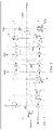
FIG. 1 is a schematic structural diagram of a gate driving circuit provided in the related art. -
FIG. 2 is a schematic timing chart for the gate driving circuit shown inFIG. 1 . -
FIG. 3 is a schematic structural diagram of a gate driving circuit provided by an embodiment of the disclosure. -
FIG. 4 is a schematic timing chart for the gate driving circuit shown inFIG. 3 . -
FIG. 5 is a specific schematic structural diagram of a shift register in which all transistors are N-type transistors provided by an embodiment of the disclosure. - The specific implementations of a gate driving circuit and a display device provided by the embodiments of the disclosure will be described in detail below with reference to the accompanying drawings.
- As shown in
FIG. 1, FIG. 1 is a schematic structural diagram of a gate driving circuit provided in the related art, which adopts 10CLK design. The gate driving circuit includes a plurality of cascaded shift registers (......GOA(n-4), GOA(n-3)......GOA(n+4), GOA(n+5)......), each shift register includes an input signal terminal IN, a reset signal terminal RS, an output control terminal OC and a gate signal output terminal G-O. The gate signal output terminals G-O are electrically connected to gate lines of a display panel in a one-to-one correspondence. In every six adjacent shift registers, such as six adjacent shift registers from GOAn to GOA(n+5), the output control terminal OC of the first shift register GOAn is electrically connected to the input signal terminal IN of the sixth shift register GOA(n+5). For six adjacent shift registers from GOA(n-1) to GOA(n+4), the output control terminal OC of the first shift register GOA(n-1) is electrically connected to the input signal terminal IN of the sixth shift register GOA(n+4), and so on. - In every seven adjacent shift registers, such as seven adjacent shift registers from GOAn to GOA(n+6), the output control terminal OC of the seventh shift register GOA(n+6) is electrically connected to the reset signal terminal RS of the first shift register GOAn; while for seven adjacent shift registers from GOA(n-1) to GOA(n+5), the output control terminal OC of the seventh shift register GOA(n+5) is electrically connected to the reset signal terminal RS of the first shift register GOA(n-1); and so on.
- A cascade structure shown in
FIG. 1 resets a first node PU in a GOA circuit by delaying the time of 1 row, so as to reverse discharge a gate line to a CLK signal through a switching transistor electrically connected to a CLK. As shown inFIG. 2, FIG. 2 is an input and output timing chart of each shift register in the gate driving circuit shown inFIG. 1 . It can be seen that in the cascade structure design ofFIG. 1 , the time of a high pulse signal and a low pulse signal of the CLK accounts for half respectively, the clock signal duty cycle only is 50%, the flexibility of an external circuit board to input a clock signal to a clock signal line is poor, and there are many cascade signal lines in the cascade structures shown inFIG. 1 , which is not conductive to saving space to further realize a narrow bezel. - In view of this, the gate driving circuit provided by the embodiment of the disclosure, as shown in
FIG. 3 , includes a plurality of cascaded shift registers (......GOA(n-4), GOA(n-3)......GOA(n+4), GOA(n+5)......), each shift register includes an input signal terminal IN, a reset signal terminal RS, an output control terminal OC and a gate signal output terminal G-O. The respective gate signal output terminals G-O are electrically connected to gate lines of a display panel in a one-to-one corresponding mode. - In every five adjacent shift registers, such as five adjacent shift registers from GOAn to GOA(n+4), the output control terminal OC of the first shift register GOAn is electrically connected to the input signal terminal IN of the fifth shift register GOA(n+4); while for five adjacent shift registers from GOA(n-1) to GOA(n+3), the output control terminal OC of the first shift register GOA(n-1) is electrically connected to the input signal terminal IN of the fifth shift register GOA(n+3), and so on.
- In every six adjacent shift registers, such as six adjacent shift registers from GOAn to GOA(n+5), the output control terminal OC of the sixth shift register GOA(n+5) is electrically connected to the reset signal terminal RS of the first shift register GOAn; for six adjacent shift registers from GOA(n-1) to GOA(n+4), the output control terminal OC of the sixth shift register GOA(n+4) is electrically connected to the reset signal terminal RS of the first shift register GOA(n-1); and so on.
- In the gate driving circuit provided by the embodiment of the disclosure, in every five adjacent shift registers, the output control terminal of the first shift register is electrically connected to the input signal terminal of the fifth shift register; and in every six adjacent shift registers, the output control terminal of the sixth shift register is electrically connected to the reset signal terminal of the first shift register, so that there are fewer cascade signal lines in the gate driving circuit of the cascade structure, thereby saving space, and further implementing the narrow bezel of a display device. In addition, for the gate driving circuit of the cascade structure provided by the disclosure, the signal provided by the external circuit board can be more flexible, even if a display product is manufactured, a pulse width of a clock signal can be adjusted by means of the external circuit board, thereby adjusting a high-level width of a gate signal output by the gate signal output terminal, and the flexibility is high.
- In the specific implementation, the gate driving circuit provided by the embodiment of the disclosure, as illustrated in
FIG. 3 , includes 10 clock signal lines (CLK1, CLK2, CLK3......CLK10), and each shift register further includes a clock signal terminal CLK. - The clock signal terminal of the (10k-9)th shift register is electrically connected to the first clock signal line, for example, clock signal terminals of first, 11th, 21th...... shift registers are electrically connected to the first clock signal line CLK1 respectively.
- The clock signal terminal of the (10k-8)th shift register is electrically connected to the second clock signal line, for example, clock signal terminals of second, 12th, 22th......shift registers are electrically connected to the second clock signal line CLK2 respectively.
- The clock signal terminal of a (10k-7)th shift register is electrically connected to the third clock signal line, for example, clock signal terminals of third, 13th, 23th......shift registers are electrically connected to the third clock signal line CLK3 respectively.
- The clock signal terminal of a (10k-6)th shift register is electrically connected to the fourth clock signal line, for example, clock signal terminals of fourth, 14th, 24th......shift registers are electrically connected to the fourth clock signal line CLK4 respectively.
- The clock signal terminal of the (10k-5)th shift register is electrically connected to the fifth clock signal line, for example, clock signal terminals of fifth, 15th, 25th......shift registers are electrically connected to the fifth clock signal line CLK5 respectively.
- The clock signal terminal of the (10k-4)th shift register is electrically connected to the sixth clock signal line, for example, clock signal terminals of sixth, 16th, 26th......shift registers are electrically connected to the sixth clock signal line CLK6 respectively.
- The clock signal terminal of the (10k-3)th shift register is electrically connected to the seventh clock signal line, for example, clock signal terminals of seventh, 17th, 27th......shift registers are electrically connected to the seventh clock signal line CLK7 respectively.
- The clock signal terminal of the (10k-2)th shift register is electrically connected to the eighth clock signal line, for example, clock signal terminals of eighth, 18th, 28th......shift registers are electrically connected to the eighth clock signal line CLK8 respectively.
- The clock signal terminal of the (10k-1)th shift register is electrically connected to the ninth clock signal line, for example, clock signal terminals of ninth, 19th, 29th......shift registers are electrically connected to the ninth clock signal line CLK9 respectively.
- The clock signal terminal of the (10k)th shift register is electrically connected to the tenth clock signal line, for example, clock signal terminals of tenth, 20th, 30th......shift registers are electrically connected to the tenth clock signal line CLK10.
- Here, k is a positive integer.
- In the specific implementation, in the gate driving circuit provided by the embodiment of the disclosure, as shown in
FIG. 4 , which is an input and output timing chart of each shift register in the gate driving circuit shown inFIG. 3 . Here a clock signal duty cycle of each clock signal line is about 40%. In this way, the cascade structure provided by the embodiment of the disclosure is adopted, so that the clock signal duty cycle of each clock signal line may be about 40%, the signal provided by the external circuit board can be more flexible, even if the display product is manufactured, the pulse width of the clock signal can be adjusted by means of the external circuit board, thereby adjusting the high-level width of the gate signal output by the gate signal output terminal, and the flexibility is high. - It should be noted that the clock signal duty cycle of each clock signal line may also be slightly higher than 40% or slightly lower than 40%, which is designed according to actual needs.
- In the specific implementation, in the gate driving circuit provided by the embodiment of the disclosure, as shown in
FIG. 5 , each shift register may include: aninput circuit 1, areset circuit 2, a control circuit, afirst output circuit 4, asecond output circuit 5 and a resetting circuit 6. In order to avoid the problem of characteristic offset or even damage of a switching transistor caused by long-time direct-current bias of a switching transistor of one control circuit, there may be two control circuits in the embodiment of the disclosure, which respectively are afirst control circuit 3 and a second control circuit 3'. A control signal terminal VDD includes a first control signal terminal VDD1 and a second control signal terminal VDD2 which are electrically connected to thefirst control circuit 3 and the second control circuit 3' respectively, and the first control signal terminal VDD1 and the second control signal terminal VDD2 alternately input valid control signals. - The
input circuit 1 is configured to control a potential of a first node PU in response to a signal input by the input signal terminal IN. - The
reset circuit 2 is configured to provide a signal input by a first reference signal terminal VSS1 to the first node PU in response to a signal input by the reset signal terminal RS. - The
first control circuit 3 is configured to provide the signal of the first reference signal terminal VSS1 to a second node PD1 in response to the signal input by the input signal terminal IN, control the potentials of the first node PU and the second node PD1 in response to a signal input by the first control signal terminal VDD1, provide a signal of a second reference signal terminal VSS2 to the gate signal output terminal G-O in response to the potential of the second node PD1, and provide the signal of the first reference signal terminal VSS1 to the output control terminal OC in response to the potential of the second node PD1. - The second control circuit 3' is configured to provide the signal of the first reference signal terminal VSS1 to a third node PD2 in response to the signal input by the input signal terminal IN, control the potentials of the first node PU and the third node PD2 in response to a signal input by the second control signal terminal VDD2, provide a signal of a second reference signal terminal VSS2 to the gate signal output terminal G-O in response to the potential of the third node PD2, and provide the signal of the first reference signal terminal VSS1 to the output control terminal OC in response to the potential of the third node PD2.
- The
first output circuit 4 is configured to provide a signal of the clock signal terminal CLK to the gate signal output terminal G-O in response to the potential of the first node PU. - The
second output circuit 5 is configured to provide the signal of the clock signal terminal CLK to the output control terminal OC in response to the potential of the first node PU. - The resetting circuit 6 is configured to provide the signal of the first reference signal terminal VSS1 to the first node PU in response to a potential of a signal input by a resetting signal terminal STV0.
- Specifically, after each frame image is output, that is, after the plurality of cascaded shift registers provided by the embodiment of the disclosure output signals, before the next frame image is output, the potentials of all first nodes PU in the plurality of cascaded shift registers are reset through the resetting circuit 6.
- In the specific implementation, in the gate driving circuit provided by the embodiment of the disclosure, as shown in
FIG. 5 , theinput circuit 1 may specifically include a first switching transistor M1; where
a gate and a first electrode of the first switching transistor M1 are electrically connected to the input signal terminal, and a second electrode is electrically connected to the first node. - The above is only an example to illustrate the specific structure of the input circuit in the shift register. In the specific implementation, the specific structure of the input circuit is not limited to the above structure provided by the embodiment of the disclosure, and may also be other structures known to those skilled in the art, which is not limited here.
- In the specific implementation, in the gate driving circuit provided by the embodiment of the disclosure, as shown in
FIG. 5 , thereset circuit 2 may include: a second switching transistor M2; and
a gate of the second switching transistor M2 is electrically connected to the reset signal terminal RS, a first electrode is electrically connected to the first node PU, and a second electrode is electrically connected to the first reference signal terminal VSS1. - The above is only an example to illustrate the specific structure of the reset circuit in the shift register. In the specific implementation, the specific structure of the reset circuit is not limited to the above structure provided by the embodiment of the disclosure, and may also be other structures known to those skilled in the art, which is not limited here.
- In the specific implementation, in the gate driving circuit provided by the embodiment of the disclosure, as shown in
FIG. 5 , thefirst control circuit 3 may include: a third switching transistor M3, a fourth switching transistor M4, a fifth switching transistor M5, a sixth switching transistor M6, a seventh switching transistor M7, an eighth switching transistor M8, a ninth switching transistor M9 and a tenth switching transistor M10. - A gate of the third switching transistor M3 is electrically connected to the input signal terminal IN, a first electrode of the third switching transistor M3 is electrically connected to the second node PD1, and a second electrode of third switching transistor M3 is electrically connected to the first reference signal terminal VSS1.
- A gate of the fourth switching transistor M4 is electrically connected to the second node PD1, a first electrode of the fourth switching transistor M4 is electrically connected to the first node PU, and a second electrode of the fourth switching transistor M4 is electrically connected to the first reference signal terminal VSS1.
- A gate of the fifth switching transistor M5 is electrically connected to the second node PD1, a first electrode of the fifth switching transistor M4 is electrically connected to the gate signal output terminal G-O of the gate driving circuit, and a second electrode of the fifth switching transistor M4 is electrically connected to the second reference signal terminal VSS2.
- A gate and a first electrode of the sixth switching transistor M6 are electrically connected to the first control signal terminal VDD1, and a second electrode of the sixth switching transistor M6 is electrically connected to a first electrode of the eighth switching transistor M8 and a gate of the seventh switching transistor M7 respectively.
- A first electrode of the seventh switching transistor M7 is electrically connected to the first control signal terminal VDD1, and a second electrode of the seventh switching transistor M7 is electrically connected to the second node PD1.
- A gate of the eighth switching transistor M8 is electrically connected to the first node PU, and a second electrode of the eighth switching transistor M8 is electrically connected to the first reference signal terminal VSS1.
- A gate of the ninth switching transistor M9 is electrically connected to the first node PU, a first electrode of the ninth switching transistor M9 is electrically connected to the second node PD1, and a second electrode of the ninth switching transistor M9 is electrically connected to the first reference signal terminal VSS1.
- A gate of the tenth switching transistor M10 is electrically connected to the second node PD1, a first electrode of the tenth switching transistor M10 is electrically connected to the output control terminal OC of the gate driving circuit, and a second electrode of the tenth switching transistor M10 is electrically connected to the first reference signal terminal VSS1.
- The second control circuit 3' may include: a fourteenth switching transistor M3', a fifteenth switching transistor M4', a sixteenth switching transistor M5', a seventeenth switching transistor M6', an eighteenth switching transistor M7', a nineteenth switching transistor M8', a twentieth switching transistor M9' and a twenty-first switching transistor M10'.
- A gate of the fourteenth switching transistor M3' is electrically connected to the input signal terminal IN, a first electrode of the fourteenth switching transistor M3' is electrically connected to the second node PD1, and a second electrode of the fourteenth switching transistor M3' is electrically connected to the first reference signal terminal VSS1.
- A gate of the fifteenth switching transistor M4' is electrically connected to the third node PD2, a first electrode of the fifteenth switching transistor M4' is electrically connected to the first node PU, and a second electrode of the fifteenth switching transistor M4' is electrically connected to the first reference signal terminal VSS1.
- A gate of the sixteenth switching transistor M5' is electrically connected to the third node PD2, a first electrode of the sixteenth switching transistor M5' is electrically connected to the gate signal output terminal G-O of the gate driving circuit, and a second electrode of the sixteenth switching transistor M5' is electrically connected to the second reference signal terminal VSS2.
- A gate and a first electrode of the seventeenth switching transistor M6' are electrically connected to the second control signal terminal VDD2, and a second electrode of the seventeenth switching transistor M6' is electrically connected to a first electrode of the nineteenth switching transistor M8' and a gate of the eighteenth switching transistor M7' respectively.
- A first electrode of the eighteenth switching transistor M7' is electrically connected to the second control signal terminal VDD2, and a second electrode of the eighteenth switching transistor M7' is electrically connected to the third node PD2.
- A gate of the nineteenth switching transistor M8' is electrically connected to the first node PU, and a second electrode of the nineteenth switching transistor M8' is electrically connected to the first reference signal terminal VSS1.
- A gate of the twentieth switching transistor M9' is electrically connected to the first node PU, a first electrode of the twentieth switching transistor M9' is electrically connected to the third node PD2, and a second electrode of the twentieth switching transistor M9' is electrically connected to the first reference signal terminal VSS1.
- A gate of the twenty-first switching transistor M10' is electrically connected to the third node PD2, a first electrode of the twenty-first switching transistor M10' is electrically connected to the output control terminal OC of the gate driving circuit, and a second electrode of the twenty-first switching transistor M10' is electrically connected to the first reference signal terminal VSS1.
- The above is only an example to illustrate the specific structures of the first control circuit and the second control circuit in the shift register. In the specific implementation, the specific structures of the first control circuit and the second control circuit are not limited to the above structures provided by the embodiment of the disclosure, and may also be other structures known to those skilled in the art, which is not limited here.
- In the specific implementation, in the gate driving circuit provided by the embodiment of the disclosure, as shown in
FIG. 5 , thefirst output circuit 4 may specifically include an eleventh switching transistor M11 and a capacitor C. - A gate of the eleventh switching transistor M11 is electrically connected to the first node PU, a first electrode of the eleventh switching transistor M11 is electrically connected to the clock signal terminal CLK, and a second electrode of the eleventh switching transistor M11 is electrically connected to the gate signal output terminal G-O of the gate driving circuit.
- The capacitor C is connected between the gate and the second electrode of the eleventh switching transistor M11.
- The above is only an example to illustrate the specific structure of the first output circuit in the shift register. In the specific implementation, the specific structure of the first output circuit is not limited to the above structure provided by the embodiment of the disclosure, and may also be other structures known to those skilled in the art, which is not limited here.
- In the specific implementation, in the gate driving circuit provided by the embodiment of the disclosure, as shown in
FIG. 5 , thesecond output circuit 5 may specifically include: a twelfth switching transistor M12; and
a gate of the twelfth switching transistor M12 is electrically connected to the first node PU, a first electrode of the twelfth switching transistor M12 is electrically connected to the clock signal terminal CLK, and a second electrode of the twelfth switching transistor M12 is electrically connected to the output control terminal OC of the gate driving circuit. - The above is only an example to illustrate the specific structure of the second output circuit in the shift register. In the specific implementation, the specific structure of the second output circuit is not limited to the above structure provided by the embodiment of the disclosure, and may also be other structures known to those skilled in the art, which is not limited here.
- In the specific implementation, in the gate driving circuit provided by the embodiment of the disclosure, as shown in
FIG. 5 , the resetting circuit 6 may specifically include: a thirteenth switching transistor M13; and
a gate of the thirteenth switching transistor M13 is electrically connected to the resetting signal terminal STV0, a first electrode of the thirteenth switching transistor M13 is electrically connected to the first node PU, and a second electrode of the thirteenth switching transistor M13 is electrically connected to the first reference signal terminal VSS1. - The above is only an example to illustrate the specific structure of the resetting circuit in the shift register. In the specific implementation, the specific structure of the resetting circuit is not limited to the above structure provided by the embodiment of the disclosure, and may also be other structures known to those skilled in the art, which is not limited here.
- It should be noted that in a normal shift register, a signal output by the gate signal output terminal G-O of this stage is used as a signal of the input signal terminal IN of the gate driving circuit of next stage, however, in the specific working process, the signal output by the gate signal output terminal G-O may fluctuate due to the influence of a gate line, resulting in unstable output. Therefore, a signal output by the second output circuit in the Nth shift register of the disclosure is output from the output control terminal OC to be used as a signal of the input signal terminal IN of a (N+4)th shift register, which can improve the stability of signal output and ensure the normal output of the gate driving circuit.
- It should be noted that the embodiment of the disclosure mainly solves the problem that in an existing 75-inch/8K/120Hz display product, there are many cascade signal lines for cascading the shift registers, and the flexibility of the external circuit board to provide clock signals to the existing gate driving circuit is poor, the input and output working principle of the gate driving circuit in a normal working state is the same as the working principle of the gate driving circuit in the related art, which will be not described in detail here.
- In the specific implementation, in the gate driving circuit provided by the embodiment of the disclosure, as shown in
FIG. 5 , all switching transistors may be N-type transistors. Potentials of the first reference signal terminal VSS1 and the second reference signal terminal VSS2 are both low potentials, the first control signal terminal VDD1 and the second control signal terminal VDD2 alternately output high and low potentials, that is, when the first control signal terminal VDD1 is at a high potential, the second control signal terminal VDD2 is at a low potential, and when the first control signal terminal VDD1 is at the low potential, the second control signal terminal VDD2 is at the high potential. - Of course, in the specific implementation, in the gate driving circuit provided by the embodiment of the disclosure, all switching transistors may also be P-type transistors.
- Moreover, in the specific implementation, the N-type transistors are turned on in response to the high potential, and are turned off in response to the low potential; and the P-type transistors are turned off in response to the high potential, and are turned on in response to the low potential.
- It should be noted that the switching transistors mentioned in the above embodiments of the disclosure may be thin film transistors (TFTs), and may also be metal oxide semiconductors (MOSs), which is not limited here. In the specific implementation, the functions of the first electrodes and the second electrodes of these switching transistors may be interchanged according to the type of the transistor and the input signals, which is not specifically distinguished. Specifically, the first electrodes of the switching transistors mentioned in the above embodiments of the disclosure may be sources, and the second electrodes may be drains; or the first electrodes may be drains, and the second electrodes may be sources, which is not specifically distinguished.
- Based on the same inventive concept, an embodiment of the disclosure further provides a display device, including the above gate driving circuit. The display device may be any display panels of products with display functions such as a mobile phone, a tablet computer, a television, a monitor, a notebook computer, a digital photo frame, a navigator, etc. The implementation of the display device may refer to the implementation of the above gate driving circuit, and the repetition will not be made.
- The embodiments of the disclosure provide the gate driving circuit and the display device. According to the gate driving circuit, in every five adjacent shift registers, the output control terminal of the first shift register is electrically connected to the input signal terminal of the fifth shift register; and in every six adjacent shift registers, the output control terminal of the sixth shift register is electrically connected to the reset signal terminal of the first shift register. In the gate driving circuit of the cascade structure provided by the disclosure, there are fewer cascade signal lines, thereby saving space, further implementing the narrow bezel of the display device; in addition, for the gate driving circuit of the cascade structure provided by the disclosure, the signal provided by the external circuit board can be more flexible, even if a display product is manufactured, the pulse width of the clock signal can be adjusted by means of the external circuit board, thereby adjusting the high-level width of the gate signal output by the gate signal output terminal, and the flexibility is high.
- Obviously, those skilled in the art can make various changes and modifications to the disclosure without departing from the spirit and scope of the disclosure. As such, provided that these modifications and variations of the disclosure fall within the scope of the claims of the disclosure and their equivalents, the disclosure is also intended to cover such modifications and variations.
Claims (12)
- A gate driving circuit, comprising a plurality of cascaded shift registers, whereineach shift register comprises an input signal terminal, a reset signal terminal, an output control terminal and a gate signal output terminal;gate signal output terminals are electrically connected to gate lines of a display panel in a one-to-one corresponding mode;in every five adjacent shift registers, an output control terminal of a first shift register among the every five adjacent shift registers is electrically connected to an input signal terminal of a fifth shift register among the every five adjacent shift registers; andin every six adjacent shift registers, an output control terminal of a sixth shift register among the every six adjacent shift registers is electrically connected to the reset signal terminal of the first shift register among the every six adjacent shift registers.
- The gate driving circuit according to claim 1, comprising 10 clock signal lines, wherein each shift register further comprises a clock signal terminal;a clock signal terminal of a (10k-9)th shift register is electrically connected to a first clock signal line;a clock signal terminal of a (10k-8)th shift register is electrically connected to a second clock signal line;a clock signal terminal of a (10k-7)th shift register is electrically connected to a third clock signal line;a clock signal terminal of a (10k-6)th shift register is electrically connected to a fourth clock signal line;a clock signal terminal of a (10k-5)th shift register is electrically connected to a fifth clock signal line;a clock signal terminal of a (10k-4)th shift register is electrically connected to a sixth clock signal line;a clock signal terminal of a (10k-3)th shift register is electrically connected to a seventh clock signal line;a clock signal terminal of a (10k-2)th shift register is electrically connected to an eighth clock signal line;a clock signal terminal of a (10k-1)th shift register is electrically connected to a ninth clock signal line; anda clock signal terminal of a (10k)th shift register is electrically connected to a tenth clock signal line; andk is a positive integer.
- The gate driving circuit according to claim 2, wherein a clock signal duty cycle of each clock signal line is approximately 40%.
- The gate driving circuit according to any one of claims 1-3, wherein each shift register comprises: an input circuit, a reset circuit, a control circuit, a first output circuit, a second output circuit and a resetting circuit; whereinthe input circuit is configured to control a potential of a first node in response to a signal input by the input signal terminal;the reset circuit is configured to provide a signal input by a first reference signal terminal to the first node in response to a signal input by the reset signal terminal;the control circuit is configured to provide the signal of the first reference signal terminal to a second node in response to the signal input by the input signal terminal, control the potentials of the first node and the second node in response to a signal input by a control signal terminal, provide a signal of a second reference signal terminal to the gate signal output terminal in response to a potential of the second node, and provide the signal of the first reference signal terminal to the output control terminal in response to the potential of the second node;the first output circuit is configured to provide a signal of the clock signal terminal to the gate signal output terminal in response to the potential of the first node;the second output circuit is configured to provide the signal of the clock signal terminal to the output control terminal in response to the potential of the first node; andthe resetting circuit is configured to provide the signal of the first reference signal terminal to the first node in response to a signal input by a resetting signal terminal.
- The gate driving circuit according to claim 4, wherein the input circuit comprises: a first switching transistor; and
a gate and a first electrode of the first switching transistor are electrically connected to the input signal terminal, and a second electrode of the first switching transistor is electrically connected to the first node. - The gate driving circuit according to claim 4, wherein the reset circuit comprises: a second switching transistor; and
a gate of the second switching transistor is electrically connected to the reset signal terminal, a first electrode of the second switching transistor is electrically connected to the first node, and a second electrode of the second switching transistor is electrically connected to the first reference signal terminal. - The gate driving circuit according to claim 4, wherein the control circuit comprises: a third switching transistor, a fourth switching transistor, a fifth switching transistor, a sixth switching transistor, a seventh switching transistor, an eighth switching transistor, a ninth switching transistor and a tenth switching transistor;a gate of the third switching transistor is electrically connected to the input signal terminal, a first electrode of the third switching transistor is electrically connected to the second node, and a second electrode of the third switching transistor is electrically connected to the first reference signal terminal;a gate of the fourth switching transistor is electrically connected to the second node, a first electrode of the fourth switching transistor is electrically connected to the first node, and a second electrode of the fourth switching transistor is electrically connected to the first reference signal terminal;a gate of the fifth switching transistor is electrically connected to the second node, a first electrode of the fifth switching transistor is electrically connected to the gate signal output terminal, and a second electrode of the fifth switching transistor is electrically connected to the second reference signal terminal;a gate and a first electrode of the sixth switching transistor are electrically connected to the control signal terminal, and a second electrode of the sixth switching transistor is electrically connected to a first electrode of the eighth switching transistor and a gate of the seventh switching transistor respectively;a first electrode of the seventh switching transistor is electrically connected to the control signal terminal, and a second electrode of the seventh switching transistor is electrically connected to the second node;a gate of the eighth switching transistor is electrically connected to the first node, and a second electrode of the eighth switching transistor is electrically connected to the first reference signal terminal;a gate of the ninth switching transistor is electrically connected to the first node, a first electrode of the ninth switching transistor is electrically connected to the second node, and a second electrode of the ninth switching transistor is electrically connected to the first reference signal terminal; anda gate of the tenth switching transistor is electrically connected to the second node, a first electrode of the tenth switching transistor is electrically connected to the output control terminal, and a second electrode of the tenth switching transistor is electrically connected to the first reference signal terminal.
- The gate driving circuit according to claim 7, wherein two said control circuits are provided and electrically connected to different control signal terminals respectively, and the two control signal terminals alternately input valid control signals.
- The gate driving circuit according to claim 4, wherein the first output circuit comprises: an eleventh switching transistor and a capacitor;a gate of the eleventh switching transistor is electrically connected to the first node, a first electrode of the eleventh switching transistor is electrically connected to the clock signal terminal, and a second electrode of the eleventh switching transistor is electrically connected to the gate signal output terminal; andthe capacitor is connected between the gate and the second electrode of the eleventh switching transistor.
- The gate driving circuit according to claim 7, wherein the second output circuit comprises: a twelfth switching transistor; and
a gate of the twelfth switching transistor is electrically connected to the first node, a first electrode of the twelfth switching transistor is electrically connected to the clock signal terminal, and a second electrode of the twelfth switching transistor is electrically connected to the output control terminal. - The gate driving circuit according to claim 4, wherein the resetting circuit comprises: a thirteenth switching transistor; and
a gate of the thirteenth switching transistor is electrically connected to the resetting signal terminal, a first electrode of the thirteenth switching transistor is electrically connected to the first node, and a second electrode of the thirteenth switching transistor is electrically connected to the first reference signal terminal. - A display device, comprising the gate driving circuit according to any one of claims 1-11.
Applications Claiming Priority (2)
| Application Number | Priority Date | Filing Date | Title |
|---|---|---|---|
| CN202010129236.0A CN111210758B (en) | 2020-02-28 | 2020-02-28 | Grid driving circuit and display device |
| PCT/CN2021/075127 WO2021169761A1 (en) | 2020-02-28 | 2021-02-03 | Gate driving circuit and display device |
Publications (2)
| Publication Number | Publication Date |
|---|---|
| EP4044164A1 true EP4044164A1 (en) | 2022-08-17 |
| EP4044164A4 EP4044164A4 (en) | 2022-12-07 |
Family
ID=70786126
Family Applications (1)
| Application Number | Title | Priority Date | Filing Date |
|---|---|---|---|
| EP21760337.2A Pending EP4044164A4 (en) | 2020-02-28 | 2021-02-03 | GATE DRIVER CIRCUIT AND INDICATOR |
Country Status (5)
| Country | Link |
|---|---|
| US (1) | US11922846B2 (en) |
| EP (1) | EP4044164A4 (en) |
| JP (1) | JP7741070B2 (en) |
| CN (1) | CN111210758B (en) |
| WO (1) | WO2021169761A1 (en) |
Cited By (1)
| Publication number | Priority date | Publication date | Assignee | Title |
|---|---|---|---|---|
| US11922846B2 (en) | 2020-02-28 | 2024-03-05 | Hefei Xinsheng Optoelectronics Technology Co., Ltd. | Gate driving circuit and display device |
Families Citing this family (5)
| Publication number | Priority date | Publication date | Assignee | Title |
|---|---|---|---|---|
| CN113838404B (en) | 2020-06-24 | 2023-01-24 | 京东方科技集团股份有限公司 | Display substrate and display device |
| CN114067712B (en) * | 2020-07-31 | 2023-09-15 | 京东方科技集团股份有限公司 | Gate drive circuit and display panel |
| CN112951140B (en) * | 2021-02-08 | 2023-12-12 | 京东方科技集团股份有限公司 | Gate driving circuit, display panel, display device and driving method |
| CN117995131B (en) * | 2024-02-21 | 2024-12-24 | 惠科股份有限公司 | Display panel and driving method of display panel |
| CN119905063B (en) * | 2025-02-28 | 2025-10-17 | 京东方科技集团股份有限公司 | Pixel circuit and driving method thereof, display panel, and display device |
Family Cites Families (20)
| Publication number | Priority date | Publication date | Assignee | Title |
|---|---|---|---|---|
| KR101542509B1 (en) | 2008-12-24 | 2015-08-06 | 삼성디스플레이 주식회사 | Gate driving device and liquid crystal display comprising therein |
| JP5436324B2 (en) * | 2010-05-10 | 2014-03-05 | 三菱電機株式会社 | Shift register circuit |
| KR20160024048A (en) | 2014-08-22 | 2016-03-04 | 삼성디스플레이 주식회사 | Display device |
| CN104537977B (en) * | 2015-01-20 | 2017-08-11 | 京东方科技集团股份有限公司 | A kind of GOA unit and driving method, GOA circuits and display device |
| CN105448258B (en) * | 2015-12-25 | 2019-01-04 | 上海中航光电子有限公司 | Gate drivers and display panel |
| CN105869566B (en) * | 2016-06-21 | 2019-12-03 | 京东方科技集团股份有限公司 | Shift register unit, driving method, gate driving circuit and display device |
| CN106448533A (en) * | 2016-09-30 | 2017-02-22 | 京东方科技集团股份有限公司 | Shift register unit, grid scanning circuit, driving method and display device |
| US10923064B2 (en) | 2017-04-17 | 2021-02-16 | Sharp Kabushiki Kaisha | Scanning signal line drive circuit and display device equipped with same |
| CN107610736B (en) * | 2017-09-27 | 2021-09-14 | 京东方科技集团股份有限公司 | Shifting register, grid driving circuit and display device |
| CN108320692B (en) | 2018-02-14 | 2022-01-07 | 京东方科技集团股份有限公司 | Shifting register unit, driving method, grid driving circuit and display panel |
| CN109979396B (en) * | 2018-02-26 | 2021-12-17 | 重庆京东方光电科技有限公司 | Grid driving circuit, touch display device and driving method |
| CN110322848B (en) | 2018-03-30 | 2021-01-08 | 京东方科技集团股份有限公司 | Shift register unit, grid driving circuit, display device and driving method |
| CN108831403B (en) | 2018-08-29 | 2020-09-04 | 合肥鑫晟光电科技有限公司 | Shifting register unit, driving method, grid driving circuit and display device |
| CN109192173A (en) | 2018-10-31 | 2019-01-11 | 京东方科技集团股份有限公司 | Gate driving circuit and its driving method, display device |
| CN109584942B (en) | 2019-01-04 | 2020-08-11 | 京东方科技集团股份有限公司 | Shifting register unit and driving method thereof, grid driving circuit and display device |
| CN109785787B (en) * | 2019-03-21 | 2022-07-01 | 合肥鑫晟光电科技有限公司 | Shift register, driving method thereof, gate driving circuit and display device |
| CN110010054B (en) | 2019-05-06 | 2023-07-28 | 京东方科技集团股份有限公司 | A gate drive circuit, a display panel, and a display device |
| CN110364110B (en) * | 2019-08-15 | 2021-03-23 | 京东方科技集团股份有限公司 | Shift register and driving method thereof, gate driving circuit, and display device |
| CN110459190B (en) | 2019-08-26 | 2021-11-05 | 京东方科技集团股份有限公司 | Shift register unit and driving method thereof, gate driving circuit, and display device |
| CN111210758B (en) | 2020-02-28 | 2023-01-31 | 合肥鑫晟光电科技有限公司 | Grid driving circuit and display device |
-
2020
- 2020-02-28 CN CN202010129236.0A patent/CN111210758B/en active Active
-
2021
- 2021-02-03 JP JP2022528944A patent/JP7741070B2/en active Active
- 2021-02-03 EP EP21760337.2A patent/EP4044164A4/en active Pending
- 2021-02-03 WO PCT/CN2021/075127 patent/WO2021169761A1/en not_active Ceased
- 2021-02-03 US US17/755,900 patent/US11922846B2/en active Active
Cited By (1)
| Publication number | Priority date | Publication date | Assignee | Title |
|---|---|---|---|---|
| US11922846B2 (en) | 2020-02-28 | 2024-03-05 | Hefei Xinsheng Optoelectronics Technology Co., Ltd. | Gate driving circuit and display device |
Also Published As
| Publication number | Publication date |
|---|---|
| US20220383804A1 (en) | 2022-12-01 |
| WO2021169761A1 (en) | 2021-09-02 |
| EP4044164A4 (en) | 2022-12-07 |
| CN111210758A (en) | 2020-05-29 |
| JP2023514908A (en) | 2023-04-12 |
| CN111210758B (en) | 2023-01-31 |
| JP7741070B2 (en) | 2025-09-17 |
| US11922846B2 (en) | 2024-03-05 |
Similar Documents
| Publication | Publication Date | Title |
|---|---|---|
| US11922846B2 (en) | Gate driving circuit and display device | |
| US10049609B2 (en) | Shift register, gate driving circuit, and display device | |
| US9847067B2 (en) | Shift register, gate driving circuit, display panel, driving method thereof and display device | |
| CN205282054U (en) | Shift register unit, gate drive circuit and display panel | |
| US10121437B2 (en) | Shift register and method for driving the same, gate driving circuit and display device | |
| CN105632562B (en) | A kind of shift register, gate driving circuit, display panel and display device | |
| EP3709287B1 (en) | Gate drive circuit and drive method therefor, and display device | |
| WO2019237956A1 (en) | Shift register and driving method therefor, gate drive circuit, and display device | |
| CN105551422B (en) | A kind of shift register, gate driving circuit and display panel | |
| CN105976749A (en) | Shift register, grid driving circuit and display panel | |
| US11393402B2 (en) | OR logic operation circuit and driving method, shift register unit, gate drive circuit, and display device | |
| CN109785787B (en) | Shift register, driving method thereof, gate driving circuit and display device | |
| US11893919B2 (en) | Gate driving circuit and display panel that alleviate trailing of a falling edge of a signal output terminal | |
| US12205555B2 (en) | Gate driving circuit and display panel | |
| CN107492338A (en) | A kind of gate driving circuit and display device | |
| US12340866B2 (en) | Shift register unit, driving method thereof, and device | |
| CN107516505A (en) | Shift register unit and its driving method, gate driving circuit and display panel | |
| CN107068083B (en) | Grid line integrated drive electronics, display panel and display device | |
| CN202363089U (en) | Shift register and array substrate grid drive circuit | |
| CN107123389A (en) | Shift register, gate driving circuit and display device | |
| CN108305581B (en) | A shift register and gate drive circuit | |
| CN106057161A (en) | Shifting register, grid line integration driving circuit, array substrate and display apparatus | |
| CN107516492B (en) | Shifting register, grid driving circuit and display device | |
| CN107507598A (en) | A kind of shift register, gate driving circuit and display device | |
| JP3146959B2 (en) | Liquid crystal display device and shift register circuit thereof |
Legal Events
| Date | Code | Title | Description |
|---|---|---|---|
| STAA | Information on the status of an ep patent application or granted ep patent |
Free format text: STATUS: THE INTERNATIONAL PUBLICATION HAS BEEN MADE |
|
| PUAI | Public reference made under article 153(3) epc to a published international application that has entered the european phase |
Free format text: ORIGINAL CODE: 0009012 |
|
| STAA | Information on the status of an ep patent application or granted ep patent |
Free format text: STATUS: REQUEST FOR EXAMINATION WAS MADE |
|
| 17P | Request for examination filed |
Effective date: 20220513 |
|
| AK | Designated contracting states |
Kind code of ref document: A1 Designated state(s): AL AT BE BG CH CY CZ DE DK EE ES FI FR GB GR HR HU IE IS IT LI LT LU LV MC MK MT NL NO PL PT RO RS SE SI SK SM TR |
|
| A4 | Supplementary search report drawn up and despatched |
Effective date: 20221108 |
|
| RIC1 | Information provided on ipc code assigned before grant |
Ipc: G09G 3/36 20060101ALI20221102BHEP Ipc: G09G 3/3266 20160101ALI20221102BHEP Ipc: G09G 3/20 20060101AFI20221102BHEP |
|
| DAV | Request for validation of the european patent (deleted) | ||
| DAX | Request for extension of the european patent (deleted) | ||
| STAA | Information on the status of an ep patent application or granted ep patent |
Free format text: STATUS: EXAMINATION IS IN PROGRESS |
|
| 17Q | First examination report despatched |
Effective date: 20240917 |