EP4040471A1 - Power semiconductor module, power semiconductor device and method for producing a power semiconductor device - Google Patents
Power semiconductor module, power semiconductor device and method for producing a power semiconductor device Download PDFInfo
- Publication number
- EP4040471A1 EP4040471A1 EP21155784.8A EP21155784A EP4040471A1 EP 4040471 A1 EP4040471 A1 EP 4040471A1 EP 21155784 A EP21155784 A EP 21155784A EP 4040471 A1 EP4040471 A1 EP 4040471A1
- Authority
- EP
- European Patent Office
- Prior art keywords
- power semiconductor
- alignment
- semiconductor module
- cooler
- alignment holes
- Prior art date
- Legal status (The legal status is an assumption and is not a legal conclusion. Google has not performed a legal analysis and makes no representation as to the accuracy of the status listed.)
- Granted
Links
Images



Classifications
-
- H—ELECTRICITY
- H05—ELECTRIC TECHNIQUES NOT OTHERWISE PROVIDED FOR
- H05K—PRINTED CIRCUITS; CASINGS OR CONSTRUCTIONAL DETAILS OF ELECTRIC APPARATUS; MANUFACTURE OF ASSEMBLAGES OF ELECTRICAL COMPONENTS
- H05K7/00—Constructional details common to different types of electric apparatus
- H05K7/20—Modifications to facilitate cooling, ventilating, or heating
- H05K7/2089—Modifications to facilitate cooling, ventilating, or heating for power electronics, e.g. for inverters for controlling motor
- H05K7/20927—Liquid coolant without phase change
-
- H—ELECTRICITY
- H10—SEMICONDUCTOR DEVICES; ELECTRIC SOLID-STATE DEVICES NOT OTHERWISE PROVIDED FOR
- H10W—GENERIC PACKAGES, INTERCONNECTIONS, CONNECTORS OR OTHER CONSTRUCTIONAL DETAILS OF DEVICES COVERED BY CLASS H10
- H10W40/00—Arrangements for thermal protection or thermal control
- H10W40/60—Securing means for detachable heating or cooling arrangements, e.g. clamps
-
- H—ELECTRICITY
- H05—ELECTRIC TECHNIQUES NOT OTHERWISE PROVIDED FOR
- H05K—PRINTED CIRCUITS; CASINGS OR CONSTRUCTIONAL DETAILS OF ELECTRIC APPARATUS; MANUFACTURE OF ASSEMBLAGES OF ELECTRICAL COMPONENTS
- H05K7/00—Constructional details common to different types of electric apparatus
- H05K7/20—Modifications to facilitate cooling, ventilating, or heating
- H05K7/20218—Modifications to facilitate cooling, ventilating, or heating using a liquid coolant without phase change in electronic enclosures
- H05K7/20254—Cold plates transferring heat from heat source to coolant
-
- H—ELECTRICITY
- H10—SEMICONDUCTOR DEVICES; ELECTRIC SOLID-STATE DEVICES NOT OTHERWISE PROVIDED FOR
- H10W—GENERIC PACKAGES, INTERCONNECTIONS, CONNECTORS OR OTHER CONSTRUCTIONAL DETAILS OF DEVICES COVERED BY CLASS H10
- H10W40/00—Arrangements for thermal protection or thermal control
- H10W40/01—Manufacture or treatment
- H10W40/03—Manufacture or treatment of arrangements for cooling
- H10W40/037—Assembling together parts thereof
-
- H—ELECTRICITY
- H10—SEMICONDUCTOR DEVICES; ELECTRIC SOLID-STATE DEVICES NOT OTHERWISE PROVIDED FOR
- H10W—GENERIC PACKAGES, INTERCONNECTIONS, CONNECTORS OR OTHER CONSTRUCTIONAL DETAILS OF DEVICES COVERED BY CLASS H10
- H10W40/00—Arrangements for thermal protection or thermal control
- H10W40/40—Arrangements for thermal protection or thermal control involving heat exchange by flowing fluids
- H10W40/47—Arrangements for thermal protection or thermal control involving heat exchange by flowing fluids by flowing liquids, e.g. forced water cooling
-
- H—ELECTRICITY
- H10—SEMICONDUCTOR DEVICES; ELECTRIC SOLID-STATE DEVICES NOT OTHERWISE PROVIDED FOR
- H10W—GENERIC PACKAGES, INTERCONNECTIONS, CONNECTORS OR OTHER CONSTRUCTIONAL DETAILS OF DEVICES COVERED BY CLASS H10
- H10W46/00—Marks applied to devices, e.g. for alignment or identification
-
- H—ELECTRICITY
- H10—SEMICONDUCTOR DEVICES; ELECTRIC SOLID-STATE DEVICES NOT OTHERWISE PROVIDED FOR
- H10W—GENERIC PACKAGES, INTERCONNECTIONS, CONNECTORS OR OTHER CONSTRUCTIONAL DETAILS OF DEVICES COVERED BY CLASS H10
- H10W70/00—Package substrates; Interposers; Redistribution layers [RDL]
- H10W70/40—Leadframes
- H10W70/421—Shapes or dispositions
-
- H—ELECTRICITY
- H10—SEMICONDUCTOR DEVICES; ELECTRIC SOLID-STATE DEVICES NOT OTHERWISE PROVIDED FOR
- H10W—GENERIC PACKAGES, INTERCONNECTIONS, CONNECTORS OR OTHER CONSTRUCTIONAL DETAILS OF DEVICES COVERED BY CLASS H10
- H10W90/00—Package configurations
-
- H—ELECTRICITY
- H10—SEMICONDUCTOR DEVICES; ELECTRIC SOLID-STATE DEVICES NOT OTHERWISE PROVIDED FOR
- H10W—GENERIC PACKAGES, INTERCONNECTIONS, CONNECTORS OR OTHER CONSTRUCTIONAL DETAILS OF DEVICES COVERED BY CLASS H10
- H10W46/00—Marks applied to devices, e.g. for alignment or identification
- H10W46/301—Marks applied to devices, e.g. for alignment or identification for alignment
Definitions
- the power semiconductor module exemplarily comprises at least two semiconductor chips.
- the two semiconductor chips are spaced apart from one another in lateral directions.
- one of the at least two semiconductor chips is formed as a switch and the other of the at least two semiconductor chips is formed as a diode.
- the switch and the diode are connected antiparallel to one another.
- the at least two semiconductor chips being connected antiparallel to one another form, for example, a half bridge.
- the power semiconductor module comprises one or more half bridges.
- the cooler comprises an inlet port and an outlet port.
- the cooler is adapted for a flow direction of a cooling medium within the cooling cavity from the inlet port to the outlet port.
- the cooling medium is pumped from the inlet port through the cooling cavity to the outlet port.
- the cooling medium is, for example, a liquid coolant or a gas coolant.
- heat generated during operation of the power semiconductor module can be dissipated away via the cooling medium effectively.
- At least one of the at least two second alignment holes can have a cross section in lateral directions being a slotted hole, circular, elliptical, oval, triangular or squared.
- the method comprises providing a fixture provided with at least two first alignment pins and with at least two second alignment pins.
- the fixture comprises a base substrate on which the first alignment pins and the second alignment pins are arranged.
- the method comprises, fixing the at least one power semiconductor module to the cooler by at least one clamp.
- the clamp is configured to press the power semiconductor module in direction to the cooler.
- the clamp is fixed exemplarily by a clamping screw to the cooler. This is to say that the clamp presses the power semiconductor module and the cooler together in vertical direction, by tightening the clamping screw for example.
- a relative position of the at least two first alignment holes with respect to the at least two second alignment holes is preset.
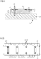
- the protruding parts 9 with the first alignment holes 10 are provided on a same lateral side of the power semiconductor module 1.
Landscapes
- Engineering & Computer Science (AREA)
- Microelectronics & Electronic Packaging (AREA)
- Physics & Mathematics (AREA)
- Thermal Sciences (AREA)
- Cooling Or The Like Of Semiconductors Or Solid State Devices (AREA)
Abstract
- at least one semiconductor chip (5) being connected to a cooling structure (3),
- at least two power terminals (7) being in electrical contact to the at least one semiconductor chip (5), and
- a housing (23) for the power semiconductor chip (5) and the at least two power terminals (7), wherein
- each of the at least two power terminals (7) has a protruding part (9) protruding beyond the housing (23) in lateral directions, and
- each of the at least two protruding parts (9) is provided with a first alignment hole (10).
Description
- The present disclosure relates to a power semiconductor module, a power semiconductor device and a method for producing a power semiconductor device.
- Exemplarily, power semiconductor modules provided with base plates having pin fins are mounted on a cooler for direct liquid cooling. For example, a correct positioning of the power semiconductor modules is needed to achieve a tight mechanical connection between the cooler and the power semiconductor module without any leakage of a cooling medium during operation. Furthermore, a correct positioning of the pin fins within the cooling cavity of the cooler provides, for example, an optimum cooling efficiency.
- When mounting several power semiconductor modules on the cooler, not only the positioning of the power semiconductor modules on the cooler itself, but also an alignment of the power semiconductor modules relative to one another is important. Only a correct alignment facilitates a proper fitting of corresponding control terminals of the power semiconductor modules to a common control board.
- Embodiments of the disclosure address in whole or in part the above shortcomings by a power semiconductor module which has an improved reliability, a power semiconductor device having such a power semiconductor module and a method for producing such a power semiconductor device.
- The exemplary embodiment of the disclosure addresses the above shortcomings by the subject-matter of the independent claims. Further exemplary embodiments are evident from the dependent claims and the following description.
- A first aspect relates to a power semiconductor device. The term "power" here and in the following, for example, refers to power semiconductor modules, semiconductor chips and power semiconductor devices adapted for processing voltages and currents of more of 100 V, e.g. more than 5000 V, and/or more than 10 A, e.g. more than 1000 A. For example, the power semiconductor module is used in automotive applications, such as electric vehicles, hybrid vehicles, motorbikes, buses, trucks, off-road construction vehicles and charging stations.
- The power semiconductor module has, for example, a main plane of extension. Lateral directions are aligned parallel to the main plane of extension and a vertical direction is aligned perpendicular to the main plane of extension.
- According to the embodiment of the first aspect, the power semiconductor module comprises at least one semiconductor chip being connected to a cooling structure.
- For example, the power semiconductor module comprises a base plate comprising a cooling structure at a first main side. Alternatively, the semiconductor module is a base plate-less power semiconductor module.
- For example, the cooling structure comprises a plurality of pin fins. Each pin fin is exemplarily formed from a pillar, wherein a tip of each pin fin extends in vertical direction facing away from the first main side. For example, all of the pin fins have a common direction of extension being parallel to the vertical direction. For example, the pin fins increase an area of a bottom surface of the base plate at the first main side.
- For example, the base plate comprises or consists of a metal, such as Cu. The pin fins are formed, for example, from the same material as the base plate, such as Cu. For example, the cooling structure and the base plate are formed integrally with one another.
- The semiconductor chip comprises, for example, a substrate or a lead frame. The substrate or the lead frame is, e.g., mounted on the base plate. The semiconductor chip is, for example, directly arranged on the substrate. Exemplarily, the at least one semiconductor chip is arranged on the base plate at a second main side opposite the first main side. The semiconductor chip is based, for example, on silicon or a wide bandgap material, exemplarily silicon carbide.
- The semiconductor chip, for example, is formed of at least one of a diode and a switch. The semiconductor chip is, exemplarily, a transistor, a varistor, an insulated gate bipolar transistor, IGBT for short, or a metal oxide semiconductor field-effect transistor, MOSFET for short, or a metal insulator semiconductor field-effect transistor, MISFET for short.
- The power semiconductor module exemplarily comprises at least two semiconductor chips. The two semiconductor chips are spaced apart from one another in lateral directions. For example, one of the at least two semiconductor chips is formed as a switch and the other of the at least two semiconductor chips is formed as a diode. In this case, the switch and the diode are connected antiparallel to one another. The at least two semiconductor chips being connected antiparallel to one another form, for example, a half bridge. For example, the power semiconductor module comprises one or more half bridges.
- According to at least one embodiment, the power semiconductor module comprises at least two power terminals being in electrical contact to at least one semiconductor chip. For example, the power terminals are configured for external contacting of the power semiconductor module, i.e. the semiconductor chip. The power terminals exemplary extend in lateral directions at least in regions. The power terminals comprise or consist, for example, of a metal, exemplarily Cu.
- For example, the power terminals show traces of an alignment process at the first side. The traces of an alignment process are, e.g. scratch marks.
- According to the embodiment, the power semiconductor module comprises a housing for the power semiconductor chip and the at least two power terminals. The housing is formed, for example, by any element being a package for the power semiconductor chip, e.g. comprising an encapsulation material such as a mold compound, a gel or a resin, e.g. a potting resin.
- For example, the housing comprises a mold compound arranged on the power semiconductor chip, the at least two power terminals and the base plate at the second main side. For example, the mold compound is in direct contact to the power semiconductor module, the power terminals and the base plate.
- The mold compound comprises or consists of an epoxy mold compound, exemplarily an epoxy resin.
- For example, the power semiconductor chip is encapsulated completely by the mold compound and the base plate. "Encapsulated" means here and in the following that the semiconductor chip is three-dimensionally encapsulated.
- Further, each of the power terminals is embedded at least in regions within the housing, e.g. the mold compound. "Embedded" means here and the following that an outer surface of each power terminal is at least in regions close to the semiconductor chip covered by the housing, e.g. the mold compound.
- According to at least one embodiment of the power semiconductor module, each of the at least two power terminals has a protruding part protruding from the housing in lateral directions. This is to say that each power terminal exemplary protrudes beyond the housing in lateral directions. The protruding parts are, for example, free of the housing. Exemplarily, the protruding parts are freely accessible in order to be externally contactable.
- According to at least one embodiment of the power semiconductor module, at least two protruding parts are provided with a first alignment hole. For example, each of the first alignment holes completely penetrates the power terminals in vertical direction.
- For example, each of the first alignment holes comprises at least one side surface. At least one of the side surfaces of at least one first alignment hole extends exemplarily in vertical direction. Alternatively, at least one of the side surfaces of at least one first alignment hole is inclined to the vertical direction. In this case, the at least one side surface of at least one first alignment hole encloses an angle with the vertical direction of at most 80°, 60°, 40° or 30° e.g. at most 20°, 10° or 5°.
- Exemplary, the power terminals can have at least one additional hole. The additional hole is exemplarily further configured to receive a screw. Exemplarily, the additional hole is configured for a screwed interconnection with an external busbar. For example, dimensions in lateral directions of the additional hole are larger than dimensions in lateral directions of the first alignment hole.
- The first alignment hole has, for example, a diameter in lateral directions of at least 0.5 mm or at least 5 mm. Further, the additional hole has, for example, a diameter being bigger than the diameter of the first alignment hole.
- In summary, such a power semiconductor module can provide, inter alia, the following advantages. For example, a correct alignment and positioning of the power semiconductor module in lateral directions can be realized with the help of the first alignment holes. Furthermore, when more than one power semiconductor module is to be positioned, the power semiconductor modules can be aligned and positioned correctly relative to one another with the help of the first alignment holes. Since such a power semiconductor module can be positioned properly, a cooling efficiency is not reduced and consequently a lifetime of the power semiconductor module is improved. Therefore, a reliability of the power semiconductor module is exemplary improved.
- According to at least one embodiment of the power semiconductor module, the at least two protruding parts are provided on a first lateral side of the power semiconductor module or on a second lateral side of the power semiconductor module opposite the first lateral side.
- According to at least one embodiment of the power semiconductor module, at least one of the at least two protruding parts are provided on a first lateral side of the power semiconductor module and at least another one of the at least two protruding parts are provided on a second lateral side of the power semiconductor module being opposite the first lateral side. This is to say that the first alignment holes are provided exemplarily on opposite lateral sides of the power semiconductor module. For example, one of the protruding parts protrudes from the housing at the first lateral side. Further, the other of the protruding parts protrudes from the housing at the second lateral side.
- According to at least one embodiment of the power semiconductor module, at least one of the at least two first alignment holes has a shape being different to at least another one of the at least two first alignment holes. Alternatively, the shapes of the at least two first alignment holes are the same.
- According to at least one embodiment of the power semiconductor module, at least one of the at least two first alignment holes has a circular shape. For example, one of the first alignment holes has a cross section aligned in lateral directions being circular.
- According to at least one embodiment of the power semiconductor module, at least another one of the at least two first alignment holes has a slotted hole shape. For example, one of the first alignment holes has a cross section aligned in lateral directions being shaped as a slotted hole.
- For an improved handling in the alignment and positioning of the power module, for example, one of the at least two first alignment holes should be circular, e.g. round, to facilitate an exact positioning in lateral directions, whereas the other one of the at least two first alignment holes should be slotted holes being sufficient for exact rotational positioning. Exemplarily, these different shapes are also considering a possible error in the positioning due to a slightly varying distance of the first alignment holes.
- Alternatively or additionally, at least one of the at least two first alignment holes can have a shape, e.g. a cross section in lateral directions, being slotted hole, elliptical, oval, triangular or squared.
- A second aspect relates to a power semiconductor device. According to the embodiment of the second aspect, the power semiconductor device comprises at least one power semiconductor module described herein above. All features disclosed in connection with the power semiconductor module are therefore also disclosed in connection with the power semiconductor device and vice versa.
- According to the embodiment, the power semiconductor device comprises a cooler on which the at least one power semiconductor module is arranged. The cooler exemplarily comprises a cooling cavity for receiving a cooling medium.
- Exemplarily the cooler comprises an inlet port and an outlet port. Exemplarily, the cooler is adapted for a flow direction of a cooling medium within the cooling cavity from the inlet port to the outlet port.
- Exemplarily, the cooling medium is pumped from the inlet port through the cooling cavity to the outlet port. The cooling medium is, for example, a liquid coolant or a gas coolant. Exemplarily, heat generated during operation of the power semiconductor module can be dissipated away via the cooling medium effectively.
- According to the embodiment of the power semiconductor device, the cooler is provided with at least two second alignment holes. For example, at least one of the second alignment holes completely penetrates the cooler in vertical direction.
- Alternatively, at least one of the second alignment holes penetrates the cooler partially. In this case the second alignment holes extend within the cooler from a bottom surface at the first main side into the cooler.
- According to the embodiment of the power semiconductor device, at least one of the at least two first alignment holes has at least one side surface extending in vertical direction or obliquely to the vertical direction.
- According to the embodiment of the power semiconductor device, at least one of the at least two second alignment holes has at least one side surface extending in vertical direction or obliquely to the vertical direction.
- For example, each of the second alignment holes comprises at least one side surface. At least one side surface of at least one second alignment hole extends exemplarily in vertical direction. Alternatively, at least one side surface of at least one second alignment hole is inclined to the vertical direction. In this case, the at least one side surface of at least one second alignment hole encloses an angle with the vertical direction of at most 80°, 60°, 40° or 30° e.g. at most 20°, 10° or 5°..
- For example, at least one of the at least two second alignment holes can have a cross section in lateral directions being a slotted hole, circular, elliptical, oval, triangular or squared.
- Exemplarily, one of the at least two second alignment holes is located in a region of a front surface of the cooler and another one of the at least two second alignment holes is located in a region of a back surface of the cooler opposite the front surface. The front surface and the back surface exemplarily extend in vertical direction. The region of the front surface extends in lateral directions in direction to the power semiconductor module and comprises, for example, the inlet port, and the region of the back surface extends in lateral directions in direction to the power semiconductor module and comprises for example the inlet port. For example, one of the at least two second alignment holes is located in a region of the inlet port and another one of the at least two second alignment holes is located in a region of the outlet port.
- Due to the first alignment holes and the second alignment holes, a correct positioning and alignment of the at least one power semiconductor module to the cooler can be achieved. Simultaneously, if more than one power semiconductor modules are present, a correct positioning and alignment of the power semiconductor modules with respect to one another can be achieved.
- According to at least one embodiment of the power semiconductor device, the cooling structure is formed integrally with the cooler. Exemplary, the cooling structure can comprise pin fins integrally formed with the cooler.
- Alternatively, the cooling structure is, for example, a cooling region without elevated structures. In this case, the cooling structure is a cooling plate integrally formed with the cooler.
- According to at least one embodiment of the power semiconductor device, the cooler is provided with at least one opening.
- For example, the cooler is provided with more than one opening. Exemplarily, the openings are provided in the cooler consecutively in the direction of the flow direction. For example, the openings are spaced apart from one another in lateral directions, e.g. along the flow direction. In this case a power semiconductor module is provided on each opening.
- Exemplarily, the power semiconductor module has a dimension in lateral directions being at least 5% larger than a dimension in lateral directions of the opening on which the power semiconductor module is arranged.
- According to at least one embodiment of the power semiconductor device, the at least one power semiconductor module is provided on the at least one opening such that the cooling structure protrudes into a cooling cavity of the cooler.
- A third aspect relates to a method for producing a power semiconductor device. For example, the method produces a power semiconductor device described herein above. Thus, all features disclosed in connection with the power semiconductor device are therefore also disclosed in connection with the method and vice versa.
- According to the embodiment of the third aspect, the method comprises providing a fixture provided with at least two first alignment pins and with at least two second alignment pins. For example, the fixture comprises a base substrate on which the first alignment pins and the second alignment pins are arranged.
- At least one of the first alignment pins and the second alignment pins is exemplarily formed from a rod, wherein a tip of the rod extends in vertical direction facing away from the fixture. For example, all first alignment pins and all second alignment pins have a common direction of extension being parallel to the vertical direction.
- Exemplary, each of the first alignment pins is configured to be insertable into a corresponding first alignment hole. The first alignment pin has a shape adapted to the corresponding first alignment hole, for example. Exemplarily, the cross section in lateral directions of the first alignment pin is at least 10 µm, e.g. at least 500 pm or at least 1 mm, smaller than the corresponding first alignment hole.
- Further, each of the second alignment pins is configured to be insertable into a corresponding second alignment hole, for example. The second alignment pin has a shape adapted to the corresponding second alignment hole, for example. Exemplarily, the cross section in lateral directions of the second alignment pin is at least 10 µm, e.g. at least 500 µm or at least 1 mm, smaller than the corresponding first alignment hole.
- According to the embodiment, the method comprises providing the at least one power semiconductor device comprising at least two power terminals being provided with at least two first alignment holes.
- According to the embodiment, the method comprises providing the cooler provided with at least two second alignment holes.
- According to the embodiment, the method comprises arranging the cooler on the fixture such that the at least two second alignment pins are introduced into the at least two second alignment holes.
- According to the embodiment, the method comprises arranging the at least one power semiconductor module on the cooler such that the at least two first alignment pins are introduced into the at least two first alignment holes.
- Exemplarily, the cooler is arranged on the fixture before the at least one power semiconductor module is arranged on the cooler.
- Due to the first alignment pins and holes and the second alignment pins and holes, a precise positioning of the power semiconductor module on the cooler can be achieved. The method provides a simple and easy method for correct and reproducible positioning and alignment. Further, a yield in an installation process of the power semiconductor module on one hand to a common control board or driver board, and on the other hand to a busbar structure of an inverter is increased. Consequently, this exemplarily results in an enhanced customer satisfactory. In addition, there is, for example, no cost adder when implementing alignment holes to the power terminals.
- According to at least one embodiment, the method comprises, fixing the at least one power semiconductor module to the cooler by at least one clamp. For example, the clamp is configured to press the power semiconductor module in direction to the cooler. The clamp is fixed exemplarily by a clamping screw to the cooler. This is to say that the clamp presses the power semiconductor module and the cooler together in vertical direction, by tightening the clamping screw for example.
- Exemplary, time needed for mounting the power semiconductor module to the cooler by screwing down clamps is reduced by the method using the first alignment pins and holes and the second alignment pins and holes and results in lower manufacturing costs. Further, by using the first alignment pins and holes and the second alignment pins and holes, exemplary, also an unwanted movement of the power semiconductor module is prevented during screwing down the clamps.
- Alternatively, the at least one power semiconductor module is fixed to the cooler by gluing, sintering or soldering.
- According to at least one embodiment of the method, a relative position of the at least two first alignment holes with respect to the at least two second alignment holes is preset.
- According to at least one embodiment of the method, at least one of the at least two first alignment pins has at least partially at least one of the shapes cylindrical, conical.
- According to at least one embodiment of the method, at least one of the at least two second alignment pins has at least partially at least one of the shapes cylindrical, conical.
- For example, at least one of the first alignment pins and the second alignment pins are formed of rods having an end region being shaped cylindrically or conically.
- For example, having an end region being conical, a self-alignment can be achieved.
- According to at least one embodiment the method comprises, providing at least one of the at least two first alignment pins and the at least two second alignment pins with a spring element. At least one of the at least two first alignment pins are provided with a spring element, for example. Further, exemplarily at least one of the at least two second alignment pins is provided with a spring element. The spring element is exemplary configured to apply a force to a respective alignment pin in vertical direction.
- According to at least one embodiment of the method, the at least one power semiconductor module further comprises at least two auxiliary terminals. For example, the auxiliary terminals are configured to provide electrical signals to the at least one power semiconductor chip. Exemplary, the auxiliary terminals are embedded in the housing, e.g. the mold compound, at least in regions. Further, each of the power terminals is embedded at least in regions within the housing, e.g. the mold compound. "Embedded" means here and the following that an outer surface of each auxiliary terminal is at least in regions close to the semiconductor chip covered by the housing, e.g. the mold compound.
- According to at least one embodiment of the method, the at least two auxiliary terminals extend at least in regions in vertical direction. Due to production tolerances, the at least two auxiliary terminals extending in vertical direction in regions can enclose an angle to the vertical direction of at most 10° or at most 5°, for example, 1°.
- For example, each of the auxiliary terminals has a further protruding part protruding from a lateral side from the housing. The further protruding parts of the auxiliary terminals extend in vertical direction at least in regions. End regions of the further protruding parts of the auxiliary terminals are configured to be directly contactable to a common control board or a driver board, exemplary by soldering or press fit connection.
- According to at least one embodiment the method comprises, arranging a common control board comprising further second alignment holes on the fixture, wherein the further second alignment holes are configured to receive the second alignment pins.
- According to at least one embodiment of the method, the common control board comprises contact holes, which are configured to receive the auxiliary terminals.
- This is to say when the common control board is mounted, the further second alignment holes of the common control board are positioned in vertical direction directly above the second alignment holes of the cooler. Exemplarily, the further second alignment holes of the common control board and the second alignment holes of the cooler are overlapping congruently.
- According to at least one embodiment the method comprises, arranging at least two power semiconductor modules, each being provided with at least two first alignment holes, on the cooler.
- Since the method enables a correct and reproducible alignment of the power semiconductor modules on the cooler and a correct and reproducible alignment of the power semiconductor modules relative to one another, a cooling medium by-pass around the cooling structure is better controlled, for example. Furthermore, all auxiliary terminals are better aligned to one another, exemplary, for better mounting of the common control board, such as a PCB, at customer side.
- The subject-matter of the disclosure will be explained in more detail in the following with reference to exemplary embodiments which are illustrated in the attached drawings.
-
Figure 1 schematically shows a three dimensional sketch of a power semiconductor module according to an exemplary embodiment. -
Figures 2 ,3, 4 and 5 each schematically show a power semiconductor device according to an exemplary embodiment. -
Figures 6, 7 and8 schematically show a method stage for producing a power semiconductor device according to an exemplary embodiment. -
Figure 9 schematically shows a power semiconductor device with a common control board according to an exemplary embodiment. -
Figures 10, 11, 12 and 13 each schematically show first alignment pins and or second alignment pins used by a method for producing a power semiconductor module according to an exemplary embodiment. - The reference symbols used in the drawings, and their meanings, are listed in summary form in the list of reference symbols. In principle, identical parts are provided with the same reference symbols in the figures.
- The
power semiconductor module 1 according to the exemplary embodiment ofFigure 1 comprises a base plate 2, alternatively a substrate, with acooling structure 3 at a first main side. Thecooling structure 3 is formed of a plurality of pin fins. - Further, at least one semiconductor chip 5 is arranged on the base plate 2 at a second main side opposite the first main side 4, not shown here since the semiconductor chip 5 is covered by a
housing 23, which is in this exemplary embodiment amold compound 8. Themold compound 8 is arranged on the power semiconductor chip 5, the at least twopower terminals 7 and the base plate 2 at the second main side 6. - In addition, the
power semiconductor module 1 comprises in this embodiment fourpower terminals 7 being in electrical contact to the at least one semiconductor chip 5. Thepower terminals 7 close to the power semiconductor chip 5 are embedded within themold compound 8. Each of thepower terminals 7 further extend beyond themold compound 8 in lateral directions. Thus, each of thepower terminals 7 has a protruding part 9 protruding from themold compound 8 in lateral directions. The protruding parts 9 are free of themold compound 8 and can be accessed freely for electrical contacting. - Two protruding parts 9, being provided on opposite lateral sides of the
power semiconductor module 1, is provided with afirst alignment hole 10. This is to say that one of thepower terminals 7 is arranged on a first lateral side 11 being provided with one of the first alignment holes 10 and another of thepower terminals 7 is arranged on a secondlateral side 12 opposite the first lateral side 11 being provided with another of the first alignment holes 10. - The
power semiconductor module 1 further comprises sevenauxiliary terminals 21 configured to provide electrical signals to the power semiconductor chip 5. Theauxiliary terminals 21 are embedded in themold compound 8 close to the power semiconductor chip 5. Theauxiliary terminals 21 extend at least in regions in vertical direction, in a region where theauxiliary terminals 21 are not embedded in themold compound 8. - The
power semiconductor device 35 according to the exemplary embodiment ofFigures 2 and3 comprises threepower semiconductor modules 1 according toFigure 1 and a cooler 13. Here,Figure 3 is a cross sectional side view of thepower semiconductor device 35 ofFigure 2 . - The cooler 13 comprises a
cooling cavity 22 for receiving a cooling medium. Further, the cooler 13 comprises aninlet port 18 and anoutlet port 19. Thus, the cooler 13 is adapted for a flow direction of a cooling medium within the coolingcavity 22 from theinlet port 18 to theoutlet port 19. - The cooler 13 is provided with three
openings 15 in this exemplary embodiment. Theopenings 15 are provided in the cooler 13 consecutively in the direction of the flow direction. In this exemplary embodiment, onepower semiconductor module 1 is provided on eachopening 15 such that each of thecooling structures 3 protrude into thecooling cavity 22 of the cooler 13. - Each of the
power semiconductor modules 1 is fixed to the cooler 13 by twoclamps 17. Further, eachclamp 17 is fixed by twoscrews 16 to the cooler 13. Directly neighbouringpower semiconductor modules 1 share oneclamp 17. Two of theclamps 17 are configured to press onepower semiconductor module 1 to the cooler 13, wherein between the cooler 13 and the power semiconductor module 1 aseal 20 is arranged. Theseal 20 can comprise a flexible material being impermeable to a cooling medium. - The cooler 13 according to
Figure 4 does not compriseopenings 15 as shown inFigure 3 . Each of thepower semiconductor modules 1 is fixed directly to the cooler 13. In this exemplary embodiment, thecooling structure 3 is formed integrally with the cooler 13 in the region in vertical direction below eachpower semiconductor module 1. - In contrast to
Figures 3 and 4 , each of thepower semiconductor modules 1 are fixed directly to the to the cooler 13 by gluing, sintering or soldering, without using aclamp 17, according toFigure 5 . - In addition, the cooler 13 is provided with two second alignment holes 14 described and shown in more detail in connection with
Figures 6, 7 and8 . - In the method stage according to
Figures 6, 7 and8 apower semiconductor device 35 according toFigure 2 is produced. Initially, afixture 25 is provided. Thefixture 25 comprises abase substrate 31 on which first alignment pins 26 and second alignment pins 27 are arranged. In this embodiment, thefixture 25 comprises six first alignment pins 26 and two second alignment pins 27. - Subsequently, a cooler 13 provided with two second alignment holes 14 is arranged on the
fixture 25 such that eachsecond alignment pin 27 is introduced into onesecond alignment hole 14. - One of the two second alignment holes 14 is located in a region of a
front surface 36 of the cooler 13 and the other one of the two second alignment holes 14 is located in a region of aback surface 37 of the cooler opposite thefront surface 36 - After the arrangement of the cooler 13 on the
fixture 25, threepower semiconductor modules 1 are arranged on the cooler 13 such that eachfirst alignment pin 26 is introduced into onefirst alignment hole 10. - In connection with
Figure 6 , the first alignment holes 10 of eachpower semiconductor module 1 are arranged on opposite lateral sides of thepower semiconductor module 1. E.g. one of the two first alignment holes 10 is located on a first lateral side 11 and the other of the two first alignment holes 10 is located on a secondlateral side 12 opposite the first lateral side 11, as shown in connection withFigure 1 . Here, theclamps 17 are connected to the cooler 13 byscrews 16. - In connection with
Figure 7 , the protruding parts 9 with the first alignment holes 10 are provided on a same lateral side of thepower semiconductor module 1. - In connection with
Figure 9 auxiliary terminals 21 of thepower semiconductor modules 1 are aligned. Theauxiliary terminals 21 can comprise pin type or press-fit type connections with which theauxiliary terminals 21 are connected to the common control board. For example, each auxiliary terminal has a pin shoulder 30 at an end region (not shown here). - A
common control board 34 is arranged on theauxiliary terminals 21. Thecommon control board 34 comprises contact holes 33 which are configured to receive theauxiliary terminals 21. Further, thecommon control board 34 comprises further second alignment holes 24, which are configured to receive the second alignment pins 27. - At least one of the
first alignment pin 26 andsecond alignment pin 27 according toFigures 10, 11, 12 and 13 are formed from of a rod, differing in their end region. The end region is configured to be inserted in at least one of thefirst alignment hole 10 andsecond alignment hole 14. The end region ofFigure 10 is cylindrical and the end region ofFigure 11 is conical. The end region ofFigure 12 is divided in two parts. The part facing the rod is formed cylindrical and the part facing away from the rod is formed conical. - At least one of the
first alignment pin 26 andsecond alignment pin 27 according toFigure 13 is further provided with aspring element 32. For example, thespring element 32 is only used when at least one of thefirst alignment pin 26 andsecond alignment pin 27 is bigger than the corresponding alignment hole and has a conical tip, in order to reduce tolerances in lateral directions to zero. Thespring element 32 is configured to apply a force in vertical direction. Exemplary, thespring element 32 is used to compensate tolerances in vertical direction. -
- 1
- power semiconductor module
- 2
- base plate
- 3
- cooling structure
- 4
- first main side
- 5
- semiconductor chip
- 6
- second main side
- 7
- power terminal
- 8
- mold compound
- 9
- protruding part
- 10
- first alignment hole
- 11
- first lateral side
- 12
- second lateral side
- 13
- cooler
- 14
- second alignment hole
- 15
- opening
- 16
- screw
- 17
- clamp
- 18
- inlet port
- 19
- outlet port
- 20
- seal
- 21
- auxiliary terminal
- 22
- cooling cavity
- 23
- housing
- 24
- further second alignment holes
- 25
- fixture
- 26
- first alignment pin
- 27
- second alignment pin
- 30
- auxiliary pin shoulder
- 31
- base substrate
- 32
- spring element
- 33
- contact holes
- 34
- control board
- 35
- power semiconductor device36 front surface
- 37
- back surface
Claims (15)
- A power semiconductor module (1), with- at least one semiconductor chip (5) being connected to a cooling structure (3),- at least two power terminals (7) being in electrical contact to the at least one semiconductor chip (5), and- a housing (23) for the power semiconductor chip (5) and the at least two power terminals (7), wherein- each of the at least two power terminals (7) has a protruding part (9) protruding beyond the housing (23) in lateral directions, and- at least two protruding parts (9) are provided with a first alignment hole (10).
- The power semiconductor module (1) according to claim 1, wherein- the at least two protruding parts (9) are provided on a first lateral side (11) of the power semiconductor module (1) or on a second lateral side (12) of the power semiconductor module (1) opposite the first lateral side (11), or- at least one of the at least two protruding parts (9) are provided on a first lateral side (11) of the power semiconductor module (1) and at least another one of the at least two protruding parts (9) are provided on a second lateral side (12) of the power semiconductor module (1) being opposite the first lateral side (11).
- The power semiconductor module (1) according to any one of the preceding claims, wherein at least one of the at least two first alignment holes (10) has a shape being different to at least another one of the at least two first alignment holes (10).
- The power semiconductor module (1) according to any one of the preceding claims, wherein- at least one of the at least two first alignment holes (10) has a circular shape, and- at least another one of the at least two first alignment holes (10) has a slotted hole shape.
- A power semiconductor device (35), with- at least one power semiconductor module (1) according to any one of the preceding claims, and- a cooler (13) on which the at least one power semiconductor module (1) is arranged, wherein- the cooler (13) is provided with at least two second alignment holes (14).
- The power semiconductor device (35) according to claim 5, wherein- the cooling structure (3) is formed integrally with the cooler (13), or- the cooler (13) is provided with at least one opening (15), and the at least one power semiconductor module (1) is provided on one of the at least one opening (15) such that the cooling structure (3) protrudes into a cooling cavity (22) of the cooler (13).
- The power semiconductor device (35) according to any one of the claims 5 to 6, wherein at least one of- each of the at least one of the at least two first alignment holes (10) has at least one side surface extending in vertical direction or obliquely to the vertical direction, and- at least one of the at least two second alignment holes (14) has at least one side surface extending in vertical direction or obliquely to the vertical direction.
- A method for producing a power semiconductor device (35) with at least one power semiconductor module (1) and a cooler (13), comprising:- providing a fixture (25) provided with at least two first alignment pins (26) and with at least two second alignment pins (27),- providing the at least one power semiconductor device (35) comprising at least two power terminals (7) being provided with at least two first alignment holes (10),- providing the cooler (13) provided with at least two second alignment holes (14),- arranging the cooler (13) on the fixture (25) such that the at least two second alignment pins (27) are introduced in the at least two second alignment holes (14), and- arranging the at least one power semiconductor module (1) on the cooler (13) such that the at least two first alignment pins (26) are introduced in the at least two first alignment holes (10).
- The method according to claim 8, wherein fixing the at least one power semiconductor module (1) to the cooler (13) by at least one clamp (17).
- The method according to any one of the claims 8 to 9, wherein a relative position of the at least two first alignment holes (10) with respect to the at least two second alignment holes (14) is pre-set.
- The method according to any one of the claims 8 to 10, wherein at least one of the at least two first alignment pins (26) has at least partially at least one of the shapes:
cylindrical, conical. - The method according to any one of the claims 8 to 11, wherein at least one of the at least two second alignment pins (27) has at least partially at least one of the shapes:
cylindrical, conical. - The method according to any one of the claims 8 to 12, wherein providing at least one of the at least two first alignment pins (26) and the at least two second alignment pins (27) with a spring element (32).
- The method according to any one of the claims 8 to 13, wherein- the at least one power semiconductor module (1) further comprises at least two auxiliary terminals (21),- the at least two auxiliary terminals (21) extend at least in regions in a vertical direction, and- arranging a common control board (33) comprising further second alignment holes (24) on the fixture (25), wherein the further second alignment holes (24) are configured to receive the second alignment pins (27), such that contact holes (33) of the common control board (34) are configured to receive the auxiliary terminals (21).
- The method according to any one of the claims 8 to 14, wherein arranging at least two power semiconductor modules (1), each being provided with at least two first alignment holes (10), on the cooler (13).
Priority Applications (5)
| Application Number | Priority Date | Filing Date | Title |
|---|---|---|---|
| EP21155784.8A EP4040471B1 (en) | 2021-02-08 | 2021-02-08 | Power semiconductor module, power semiconductor device and method for producing a power semiconductor device |
| PCT/EP2022/051903 WO2022167317A1 (en) | 2021-02-08 | 2022-01-27 | Power semiconductor module, power semiconductor device and method for producing a power semiconductor device |
| US18/276,237 US20240120255A1 (en) | 2021-02-08 | 2022-01-27 | Power semiconductor module, power semiconductor device and method for producing a power semiconductor device |
| CN202280013845.7A CN116830247B (en) | 2021-02-08 | 2022-01-27 | Power semiconductor module, power semiconductor device and method for producing a power semiconductor device |
| JP2023547661A JP7685063B2 (en) | 2021-02-08 | 2022-01-27 | POWER SEMICONDUCTOR MODULE, POWER SEMICONDUCTOR DEVICE AND METHOD FOR FABRICATING A POWER SEMICONDUCTOR DEVICE - Patent application |
Applications Claiming Priority (1)
| Application Number | Priority Date | Filing Date | Title |
|---|---|---|---|
| EP21155784.8A EP4040471B1 (en) | 2021-02-08 | 2021-02-08 | Power semiconductor module, power semiconductor device and method for producing a power semiconductor device |
Publications (2)
| Publication Number | Publication Date |
|---|---|
| EP4040471A1 true EP4040471A1 (en) | 2022-08-10 |
| EP4040471B1 EP4040471B1 (en) | 2025-08-06 |
Family
ID=74561780
Family Applications (1)
| Application Number | Title | Priority Date | Filing Date |
|---|---|---|---|
| EP21155784.8A Active EP4040471B1 (en) | 2021-02-08 | 2021-02-08 | Power semiconductor module, power semiconductor device and method for producing a power semiconductor device |
Country Status (5)
| Country | Link |
|---|---|
| US (1) | US20240120255A1 (en) |
| EP (1) | EP4040471B1 (en) |
| JP (1) | JP7685063B2 (en) |
| CN (1) | CN116830247B (en) |
| WO (1) | WO2022167317A1 (en) |
Families Citing this family (2)
| Publication number | Priority date | Publication date | Assignee | Title |
|---|---|---|---|---|
| US20240064944A1 (en) * | 2022-08-17 | 2024-02-22 | Semiconductor Components Industries, Llc | Sealing method for direct liquid cooled power electronics package |
| US12122251B2 (en) * | 2022-09-28 | 2024-10-22 | BorgWarner US Technologies LLC | Systems and methods for bidirectional message architecture for inverter for electric vehicle |
Citations (7)
| Publication number | Priority date | Publication date | Assignee | Title |
|---|---|---|---|---|
| JP2001168278A (en) * | 1999-12-09 | 2001-06-22 | Toshiba Corp | Power semiconductor module and power converter |
| JP2006086438A (en) * | 2004-09-17 | 2006-03-30 | Nichicon Corp | Semiconductor module bus bar structure |
| EP2395647A1 (en) * | 2009-02-06 | 2011-12-14 | Hitachi Automotive Systems, Ltd. | Power converter |
| WO2013140704A1 (en) * | 2012-03-21 | 2013-09-26 | 富士電機株式会社 | Power conversion apparatus |
| JP2015128138A (en) * | 2013-11-27 | 2015-07-09 | 株式会社豊田自動織機 | Semiconductor device |
| US20170110341A1 (en) * | 2014-03-26 | 2017-04-20 | Denso Corporation | Semiconductor device manufacturing method |
| DE102019202903A1 (en) * | 2019-03-04 | 2020-09-10 | Abb Schweiz Ag | Electronic converter trained based on welding technologies |
Family Cites Families (37)
| Publication number | Priority date | Publication date | Assignee | Title |
|---|---|---|---|---|
| US3381554A (en) * | 1967-06-30 | 1968-05-07 | Mcdonnell Aircraft Corp | Bushings for locating two adjaent parts |
| US3763730A (en) * | 1972-01-27 | 1973-10-09 | O Ahlegian | Optical hole film punch |
| US3918694A (en) * | 1974-05-06 | 1975-11-11 | Richard D Laudick | Locator pin |
| JP2684863B2 (en) * | 1991-04-02 | 1997-12-03 | 三菱電機株式会社 | Semiconductor device |
| US6309601B1 (en) * | 1993-11-01 | 2001-10-30 | Nanogen, Inc. | Scanning optical detection system |
| US6273554B1 (en) * | 2000-04-25 | 2001-08-14 | Hewlett-Packard Company | Apparatus for aligning a flexible circuit on a ink jet printer carriage |
| US8169780B2 (en) * | 2009-06-18 | 2012-05-01 | Honda Motor Co., Ltd. | Power conversion device |
| JP4724245B2 (en) * | 2009-12-25 | 2011-07-13 | 株式会社東芝 | Electronics |
| GB2512559B (en) * | 2010-07-05 | 2016-02-24 | Tb Composites Ltd | Bridge superstructure decking panel and attachment system |
| WO2012051704A1 (en) * | 2010-10-19 | 2012-04-26 | Electronic Motion Systems Holdings Limited | A power module for converting dc to ac |
| DE112013003222B4 (en) * | 2012-06-29 | 2021-08-19 | Denso Corporation | Semiconductor device and semiconductor device connection structure |
| CN203503643U (en) * | 2013-08-27 | 2014-03-26 | 南京银茂微电子制造有限公司 | Power module free of bending of power terminals |
| DE102014111995B4 (en) * | 2014-08-21 | 2022-10-13 | Infineon Technologies Ag | METHODS OF GRASPING, MOVING AND ELECTRICAL TESTING OF A SEMICONDUCTOR MODULE |
| CN104900640A (en) * | 2015-05-06 | 2015-09-09 | 嘉兴斯达微电子有限公司 | Power semiconductor module with snap ring structured shell |
| WO2017195283A1 (en) * | 2016-05-11 | 2017-11-16 | 日立オートモティブシステムズ株式会社 | Power semiconductor module, power conversion device using same, and method for manufacturing power conversion device |
| CN205921880U (en) * | 2016-07-22 | 2017-02-01 | 江森自控空调冷冻设备(无锡)有限公司 | A cold drawing subassembly for regulator cubicle |
| EP3545550B1 (en) * | 2016-11-23 | 2021-02-17 | ABB Schweiz AG | Manufacturing of a power semiconductor module |
| CN110050339B (en) * | 2016-12-16 | 2023-12-22 | 日立能源有限公司 | Power semiconductor modules with low gate path inductance |
| JP6750514B2 (en) * | 2017-01-18 | 2020-09-02 | 株式会社デンソー | Semiconductor device |
| CN110622307B (en) * | 2017-05-12 | 2023-06-16 | 三菱电机株式会社 | Semiconductor module and power conversion device |
| WO2018224511A1 (en) * | 2017-06-07 | 2018-12-13 | Abb Schweiz Ag | Power semiconductor module |
| CN107170714B (en) * | 2017-06-14 | 2020-01-14 | 扬州国扬电子有限公司 | Low parasitic inductance power module and double-sided heat dissipation low parasitic inductance power module |
| CN107403783B (en) * | 2017-08-30 | 2023-10-31 | 扬州国扬电子有限公司 | A parallel electrode combination, power module and power module |
| JP6899784B2 (en) * | 2018-01-17 | 2021-07-07 | 日立Astemo株式会社 | Power semiconductor device |
| CN110323142B (en) * | 2018-03-29 | 2021-08-31 | 台达电子工业股份有限公司 | Power module and method of manufacturing the same |
| JP7100569B2 (en) * | 2018-11-22 | 2022-07-13 | 日立Astemo株式会社 | Manufacturing method of semiconductor modules, power converters and semiconductor modules |
| JP7124769B2 (en) * | 2019-03-06 | 2022-08-24 | 株式会社デンソー | semiconductor module |
| JP6750809B1 (en) * | 2019-04-22 | 2020-09-02 | 三菱電機株式会社 | Cooler |
| DE102019114001A1 (en) * | 2019-05-24 | 2020-11-26 | Schaeffler Technologies AG & Co. KG | Power electronics unit with at least one semiconductor module connected by means of a plastic holder |
| US11309649B2 (en) * | 2019-05-31 | 2022-04-19 | Apple Inc. | Floating connector assembly |
| DE102019213385A1 (en) * | 2019-09-04 | 2021-03-04 | Zf Friedrichshafen Ag | Control device for operating an electric drive for a vehicle and method for producing such a control device |
| JP7419050B2 (en) * | 2019-12-16 | 2024-01-22 | 日立Astemo株式会社 | Power module, power converter, and power module manufacturing method |
| DE102021000513A1 (en) * | 2020-02-10 | 2021-08-12 | Semiconductor Components lndustries, LLC | INTEGRATION OF SEMI-CONDUCTOR DEVICE ARRANGEMENTS IN HEAT DISSIPATION MECHANISMS |
| US11961782B2 (en) * | 2020-02-10 | 2024-04-16 | Semiconductor Components Industries, Llc | Integration of semiconductor device assemblies with thermal dissipation mechanisms |
| JPWO2021176996A1 (en) * | 2020-03-04 | 2021-09-10 | ||
| JP7677066B2 (en) * | 2021-08-26 | 2025-05-15 | 富士電機株式会社 | Semiconductor device and method for manufacturing the same |
| CN114334921B (en) * | 2021-12-31 | 2025-07-01 | 佛山市国星光电股份有限公司 | Power module and cooling system |
-
2021
- 2021-02-08 EP EP21155784.8A patent/EP4040471B1/en active Active
-
2022
- 2022-01-27 WO PCT/EP2022/051903 patent/WO2022167317A1/en not_active Ceased
- 2022-01-27 JP JP2023547661A patent/JP7685063B2/en active Active
- 2022-01-27 CN CN202280013845.7A patent/CN116830247B/en active Active
- 2022-01-27 US US18/276,237 patent/US20240120255A1/en active Pending
Patent Citations (7)
| Publication number | Priority date | Publication date | Assignee | Title |
|---|---|---|---|---|
| JP2001168278A (en) * | 1999-12-09 | 2001-06-22 | Toshiba Corp | Power semiconductor module and power converter |
| JP2006086438A (en) * | 2004-09-17 | 2006-03-30 | Nichicon Corp | Semiconductor module bus bar structure |
| EP2395647A1 (en) * | 2009-02-06 | 2011-12-14 | Hitachi Automotive Systems, Ltd. | Power converter |
| WO2013140704A1 (en) * | 2012-03-21 | 2013-09-26 | 富士電機株式会社 | Power conversion apparatus |
| JP2015128138A (en) * | 2013-11-27 | 2015-07-09 | 株式会社豊田自動織機 | Semiconductor device |
| US20170110341A1 (en) * | 2014-03-26 | 2017-04-20 | Denso Corporation | Semiconductor device manufacturing method |
| DE102019202903A1 (en) * | 2019-03-04 | 2020-09-10 | Abb Schweiz Ag | Electronic converter trained based on welding technologies |
Also Published As
| Publication number | Publication date |
|---|---|
| WO2022167317A1 (en) | 2022-08-11 |
| US20240120255A1 (en) | 2024-04-11 |
| JP2024505712A (en) | 2024-02-07 |
| JP7685063B2 (en) | 2025-05-28 |
| EP4040471B1 (en) | 2025-08-06 |
| CN116830247B (en) | 2024-08-09 |
| CN116830247A (en) | 2023-09-29 |
Similar Documents
| Publication | Publication Date | Title |
|---|---|---|
| US9379083B2 (en) | Semiconductor device and method for manufacturing semiconductor device | |
| US9385061B2 (en) | Semiconductor device and method for manufacturing semiconductor device | |
| US9312192B2 (en) | Semiconductor device | |
| US9147649B2 (en) | Multi-chip module | |
| US11251108B2 (en) | Semiconductor module mounted on a cooling device for use in a vehicle | |
| US7508068B2 (en) | Semiconductor module and power conversion device | |
| US11018076B2 (en) | Cooling apparatus, semiconductor module, and vehicle | |
| US11631641B2 (en) | Semiconductor device, semiconductor module, and vehicle | |
| US10699978B2 (en) | SMD package with top side cooling | |
| CN111816572B (en) | Chip package and forming method thereof, semiconductor device and forming method thereof, semiconductor device and forming method thereof, three-phase system | |
| CN105684147A (en) | Semiconductor module and manufacturing method thereof | |
| US10903149B2 (en) | Semiconductor module, electric vehicle, and power control unit | |
| US11217511B2 (en) | Quad package with conductive clips connected to terminals at upper surface of semiconductor die | |
| US20240120255A1 (en) | Power semiconductor module, power semiconductor device and method for producing a power semiconductor device | |
| EP1378941B1 (en) | Semiconductor module and power conversion device | |
| JP2020092250A (en) | Semiconductor module, vehicle and manufacturing method | |
| US11937413B2 (en) | Power electronics module and method for fabricating a power electronics module | |
| US10699987B2 (en) | SMD package with flat contacts to prevent bottleneck | |
| JPWO2020035931A1 (en) | Semiconductor module | |
| CN113644038A (en) | Semiconductor Modules and Vehicles | |
| JP2020501380A (en) | Manufacture of power semiconductor modules | |
| CN114365282B (en) | Semiconductor module | |
| US7229855B2 (en) | Process for assembling a double-sided circuit component | |
| US20250070104A1 (en) | Power electronic system having a power semiconductor module and a current sensor and power semiconductor module | |
| CN222395577U (en) | Copper busbar structure, motor controller and vehicle |
Legal Events
| Date | Code | Title | Description |
|---|---|---|---|
| PUAI | Public reference made under article 153(3) epc to a published international application that has entered the european phase |
Free format text: ORIGINAL CODE: 0009012 |
|
| STAA | Information on the status of an ep patent application or granted ep patent |
Free format text: STATUS: THE APPLICATION HAS BEEN PUBLISHED |
|
| AK | Designated contracting states |
Kind code of ref document: A1 Designated state(s): AL AT BE BG CH CY CZ DE DK EE ES FI FR GB GR HR HU IE IS IT LI LT LU LV MC MK MT NL NO PL PT RO RS SE SI SK SM TR |
|
| STAA | Information on the status of an ep patent application or granted ep patent |
Free format text: STATUS: REQUEST FOR EXAMINATION WAS MADE |
|
| 17P | Request for examination filed |
Effective date: 20230111 |
|
| RBV | Designated contracting states (corrected) |
Designated state(s): AL AT BE BG CH CY CZ DE DK EE ES FI FR GB GR HR HU IE IS IT LI LT LU LV MC MK MT NL NO PL PT RO RS SE SI SK SM TR |
|
| P01 | Opt-out of the competence of the unified patent court (upc) registered |
Effective date: 20230527 |
|
| RAP1 | Party data changed (applicant data changed or rights of an application transferred) |
Owner name: HITACHI ENERGY LTD |
|
| RIC1 | Information provided on ipc code assigned before grant |
Ipc: H01L 25/18 20060101ALI20250220BHEP Ipc: H01L 23/40 20060101ALI20250220BHEP Ipc: H01L 23/473 20060101ALI20250220BHEP Ipc: H01L 23/495 20060101ALI20250220BHEP Ipc: H01L 23/544 20060101ALI20250220BHEP Ipc: H01L 25/07 20060101ALI20250220BHEP Ipc: H01L 21/48 20060101AFI20250220BHEP |
|
| GRAP | Despatch of communication of intention to grant a patent |
Free format text: ORIGINAL CODE: EPIDOSNIGR1 |
|
| STAA | Information on the status of an ep patent application or granted ep patent |
Free format text: STATUS: GRANT OF PATENT IS INTENDED |
|
| INTG | Intention to grant announced |
Effective date: 20250408 |
|
| GRAS | Grant fee paid |
Free format text: ORIGINAL CODE: EPIDOSNIGR3 |
|
| GRAA | (expected) grant |
Free format text: ORIGINAL CODE: 0009210 |
|
| STAA | Information on the status of an ep patent application or granted ep patent |
Free format text: STATUS: THE PATENT HAS BEEN GRANTED |
|
| AK | Designated contracting states |
Kind code of ref document: B1 Designated state(s): AL AT BE BG CH CY CZ DE DK EE ES FI FR GB GR HR HU IE IS IT LI LT LU LV MC MK MT NL NO PL PT RO RS SE SI SK SM TR |
|
| REG | Reference to a national code |
Ref country code: GB Ref legal event code: FG4D |
|
| REG | Reference to a national code |
Ref country code: CH Ref legal event code: EP |
|
| REG | Reference to a national code |
Ref country code: DE Ref legal event code: R096 Ref document number: 602021035415 Country of ref document: DE |
|
| REG | Reference to a national code |
Ref country code: IE Ref legal event code: FG4D |
|
| REG | Reference to a national code |
Ref country code: DE Ref legal event code: R079 Ref document number: 602021035415 Country of ref document: DE Free format text: PREVIOUS MAIN CLASS: H01L0021480000 Ipc: H10W0076010000 |
|
| REG | Reference to a national code |
Ref country code: NL Ref legal event code: MP Effective date: 20250806 |
|
| PG25 | Lapsed in a contracting state [announced via postgrant information from national office to epo] |
Ref country code: IS Free format text: LAPSE BECAUSE OF FAILURE TO SUBMIT A TRANSLATION OF THE DESCRIPTION OR TO PAY THE FEE WITHIN THE PRESCRIBED TIME-LIMIT Effective date: 20251206 |
|
| PG25 | Lapsed in a contracting state [announced via postgrant information from national office to epo] |
Ref country code: NO Free format text: LAPSE BECAUSE OF FAILURE TO SUBMIT A TRANSLATION OF THE DESCRIPTION OR TO PAY THE FEE WITHIN THE PRESCRIBED TIME-LIMIT Effective date: 20251106 |
|
| REG | Reference to a national code |
Ref country code: LT Ref legal event code: MG9D |
|
| PG25 | Lapsed in a contracting state [announced via postgrant information from national office to epo] |
Ref country code: PT Free format text: LAPSE BECAUSE OF FAILURE TO SUBMIT A TRANSLATION OF THE DESCRIPTION OR TO PAY THE FEE WITHIN THE PRESCRIBED TIME-LIMIT Effective date: 20251209 |
|
| PG25 | Lapsed in a contracting state [announced via postgrant information from national office to epo] |
Ref country code: FI Free format text: LAPSE BECAUSE OF FAILURE TO SUBMIT A TRANSLATION OF THE DESCRIPTION OR TO PAY THE FEE WITHIN THE PRESCRIBED TIME-LIMIT Effective date: 20250806 |
|
| PG25 | Lapsed in a contracting state [announced via postgrant information from national office to epo] |
Ref country code: NL Free format text: LAPSE BECAUSE OF FAILURE TO SUBMIT A TRANSLATION OF THE DESCRIPTION OR TO PAY THE FEE WITHIN THE PRESCRIBED TIME-LIMIT Effective date: 20250806 Ref country code: HR Free format text: LAPSE BECAUSE OF FAILURE TO SUBMIT A TRANSLATION OF THE DESCRIPTION OR TO PAY THE FEE WITHIN THE PRESCRIBED TIME-LIMIT Effective date: 20250806 |
|
| PG25 | Lapsed in a contracting state [announced via postgrant information from national office to epo] |
Ref country code: GR Free format text: LAPSE BECAUSE OF FAILURE TO SUBMIT A TRANSLATION OF THE DESCRIPTION OR TO PAY THE FEE WITHIN THE PRESCRIBED TIME-LIMIT Effective date: 20251107 |
|
| PG25 | Lapsed in a contracting state [announced via postgrant information from national office to epo] |
Ref country code: SE Free format text: LAPSE BECAUSE OF FAILURE TO SUBMIT A TRANSLATION OF THE DESCRIPTION OR TO PAY THE FEE WITHIN THE PRESCRIBED TIME-LIMIT Effective date: 20250806 |
|
| PG25 | Lapsed in a contracting state [announced via postgrant information from national office to epo] |
Ref country code: LV Free format text: LAPSE BECAUSE OF FAILURE TO SUBMIT A TRANSLATION OF THE DESCRIPTION OR TO PAY THE FEE WITHIN THE PRESCRIBED TIME-LIMIT Effective date: 20250806 |
|
| PG25 | Lapsed in a contracting state [announced via postgrant information from national office to epo] |
Ref country code: PL Free format text: LAPSE BECAUSE OF FAILURE TO SUBMIT A TRANSLATION OF THE DESCRIPTION OR TO PAY THE FEE WITHIN THE PRESCRIBED TIME-LIMIT Effective date: 20250806 Ref country code: BG Free format text: LAPSE BECAUSE OF FAILURE TO SUBMIT A TRANSLATION OF THE DESCRIPTION OR TO PAY THE FEE WITHIN THE PRESCRIBED TIME-LIMIT Effective date: 20250806 |
|
| PG25 | Lapsed in a contracting state [announced via postgrant information from national office to epo] |
Ref country code: RS Free format text: LAPSE BECAUSE OF FAILURE TO SUBMIT A TRANSLATION OF THE DESCRIPTION OR TO PAY THE FEE WITHIN THE PRESCRIBED TIME-LIMIT Effective date: 20251106 |
|
| PG25 | Lapsed in a contracting state [announced via postgrant information from national office to epo] |
Ref country code: ES Free format text: LAPSE BECAUSE OF FAILURE TO SUBMIT A TRANSLATION OF THE DESCRIPTION OR TO PAY THE FEE WITHIN THE PRESCRIBED TIME-LIMIT Effective date: 20250806 |
|
| REG | Reference to a national code |
Ref country code: AT Ref legal event code: MK05 Ref document number: 1822983 Country of ref document: AT Kind code of ref document: T Effective date: 20250806 |
|
| PG25 | Lapsed in a contracting state [announced via postgrant information from national office to epo] |
Ref country code: SM Free format text: LAPSE BECAUSE OF FAILURE TO SUBMIT A TRANSLATION OF THE DESCRIPTION OR TO PAY THE FEE WITHIN THE PRESCRIBED TIME-LIMIT Effective date: 20250806 |
|
| PGFP | Annual fee paid to national office [announced via postgrant information from national office to epo] |
Ref country code: GB Payment date: 20260220 Year of fee payment: 6 |
|
| PG25 | Lapsed in a contracting state [announced via postgrant information from national office to epo] |
Ref country code: DK Free format text: LAPSE BECAUSE OF FAILURE TO SUBMIT A TRANSLATION OF THE DESCRIPTION OR TO PAY THE FEE WITHIN THE PRESCRIBED TIME-LIMIT Effective date: 20250806 |
|
| PGFP | Annual fee paid to national office [announced via postgrant information from national office to epo] |
Ref country code: DE Payment date: 20260218 Year of fee payment: 6 |
|
| PG25 | Lapsed in a contracting state [announced via postgrant information from national office to epo] |
Ref country code: AT Free format text: LAPSE BECAUSE OF FAILURE TO SUBMIT A TRANSLATION OF THE DESCRIPTION OR TO PAY THE FEE WITHIN THE PRESCRIBED TIME-LIMIT Effective date: 20250806 |
|
| PG25 | Lapsed in a contracting state [announced via postgrant information from national office to epo] |
Ref country code: IT Free format text: LAPSE BECAUSE OF FAILURE TO SUBMIT A TRANSLATION OF THE DESCRIPTION OR TO PAY THE FEE WITHIN THE PRESCRIBED TIME-LIMIT Effective date: 20250806 |
|
| PG25 | Lapsed in a contracting state [announced via postgrant information from national office to epo] |
Ref country code: CZ Free format text: LAPSE BECAUSE OF FAILURE TO SUBMIT A TRANSLATION OF THE DESCRIPTION OR TO PAY THE FEE WITHIN THE PRESCRIBED TIME-LIMIT Effective date: 20250806 |
|
| PG25 | Lapsed in a contracting state [announced via postgrant information from national office to epo] |
Ref country code: SK Free format text: LAPSE BECAUSE OF FAILURE TO SUBMIT A TRANSLATION OF THE DESCRIPTION OR TO PAY THE FEE WITHIN THE PRESCRIBED TIME-LIMIT Effective date: 20250806 Ref country code: EE Free format text: LAPSE BECAUSE OF FAILURE TO SUBMIT A TRANSLATION OF THE DESCRIPTION OR TO PAY THE FEE WITHIN THE PRESCRIBED TIME-LIMIT Effective date: 20250806 |