EP4040468A1 - Method for manufacturing semiconductor element, and semiconductor device - Google Patents
Method for manufacturing semiconductor element, and semiconductor device Download PDFInfo
- Publication number
- EP4040468A1 EP4040468A1 EP20872323.9A EP20872323A EP4040468A1 EP 4040468 A1 EP4040468 A1 EP 4040468A1 EP 20872323 A EP20872323 A EP 20872323A EP 4040468 A1 EP4040468 A1 EP 4040468A1
- Authority
- EP
- European Patent Office
- Prior art keywords
- semiconductor
- mask
- manufacturing
- semiconductor element
- substrate
- Prior art date
- Legal status (The legal status is an assumption and is not a legal conclusion. Google has not performed a legal analysis and makes no representation as to the accuracy of the status listed.)
- Withdrawn
Links
Images
Classifications
-
- H—ELECTRICITY
- H10—SEMICONDUCTOR DEVICES; ELECTRIC SOLID-STATE DEVICES NOT OTHERWISE PROVIDED FOR
- H10P—GENERIC PROCESSES OR APPARATUS FOR THE MANUFACTURE OR TREATMENT OF DEVICES COVERED BY CLASS H10
- H10P14/00—Formation of materials, e.g. in the shape of layers or pillars
- H10P14/20—Formation of materials, e.g. in the shape of layers or pillars of semiconductor materials
- H10P14/27—Formation of materials, e.g. in the shape of layers or pillars of semiconductor materials using selective deposition, e.g. simultaneous growth of monocrystalline and non-monocrystalline semiconductor materials
- H10P14/271—Formation of materials, e.g. in the shape of layers or pillars of semiconductor materials using selective deposition, e.g. simultaneous growth of monocrystalline and non-monocrystalline semiconductor materials characterised by the preparation of substrate for selective deposition
-
- H—ELECTRICITY
- H10—SEMICONDUCTOR DEVICES; ELECTRIC SOLID-STATE DEVICES NOT OTHERWISE PROVIDED FOR
- H10D—INORGANIC ELECTRIC SEMICONDUCTOR DEVICES
- H10D30/00—Field-effect transistors [FET]
- H10D30/60—Insulated-gate field-effect transistors [IGFET]
- H10D30/67—Thin-film transistors [TFT]
- H10D30/6729—Thin-film transistors [TFT] characterised by the electrodes
- H10D30/6737—Thin-film transistors [TFT] characterised by the electrodes characterised by the electrode materials
- H10D30/6738—Schottky barrier electrodes
-
- H—ELECTRICITY
- H10—SEMICONDUCTOR DEVICES; ELECTRIC SOLID-STATE DEVICES NOT OTHERWISE PROVIDED FOR
- H10D—INORGANIC ELECTRIC SEMICONDUCTOR DEVICES
- H10D30/00—Field-effect transistors [FET]
- H10D30/60—Insulated-gate field-effect transistors [IGFET]
- H10D30/67—Thin-film transistors [TFT]
- H10D30/674—Thin-film transistors [TFT] characterised by the active materials
- H10D30/675—Group III-V materials, Group II-VI materials, Group IV-VI materials, selenium or tellurium
-
- H—ELECTRICITY
- H10—SEMICONDUCTOR DEVICES; ELECTRIC SOLID-STATE DEVICES NOT OTHERWISE PROVIDED FOR
- H10D—INORGANIC ELECTRIC SEMICONDUCTOR DEVICES
- H10D62/00—Semiconductor bodies, or regions thereof, of devices having potential barriers
- H10D62/10—Shapes, relative sizes or dispositions of the regions of the semiconductor bodies; Shapes of the semiconductor bodies
- H10D62/102—Constructional design considerations for preventing surface leakage or controlling electric field concentration
- H10D62/103—Constructional design considerations for preventing surface leakage or controlling electric field concentration for increasing or controlling the breakdown voltage of reverse-biased devices
- H10D62/105—Constructional design considerations for preventing surface leakage or controlling electric field concentration for increasing or controlling the breakdown voltage of reverse-biased devices by having particular doping profiles, shapes or arrangements of PN junctions; by having supplementary regions, e.g. junction termination extension [JTE]
- H10D62/106—Constructional design considerations for preventing surface leakage or controlling electric field concentration for increasing or controlling the breakdown voltage of reverse-biased devices by having particular doping profiles, shapes or arrangements of PN junctions; by having supplementary regions, e.g. junction termination extension [JTE] having supplementary regions doped oppositely to or in rectifying contact with regions of the semiconductor bodies, e.g. guard rings with PN or Schottky junctions
- H10D62/107—Buried supplementary regions, e.g. buried guard rings
-
- H—ELECTRICITY
- H10—SEMICONDUCTOR DEVICES; ELECTRIC SOLID-STATE DEVICES NOT OTHERWISE PROVIDED FOR
- H10D—INORGANIC ELECTRIC SEMICONDUCTOR DEVICES
- H10D62/00—Semiconductor bodies, or regions thereof, of devices having potential barriers
- H10D62/80—Semiconductor bodies, or regions thereof, of devices having potential barriers characterised by the materials
- H10D62/85—Semiconductor bodies, or regions thereof, of devices having potential barriers characterised by the materials being Group III-V materials, e.g. GaAs
- H10D62/8503—Nitride Group III-V materials, e.g. AlN or GaN
-
- H—ELECTRICITY
- H10—SEMICONDUCTOR DEVICES; ELECTRIC SOLID-STATE DEVICES NOT OTHERWISE PROVIDED FOR
- H10D—INORGANIC ELECTRIC SEMICONDUCTOR DEVICES
- H10D64/00—Electrodes of devices having potential barriers
- H10D64/20—Electrodes characterised by their shapes, relative sizes or dispositions
- H10D64/23—Electrodes carrying the current to be rectified, amplified, oscillated or switched, e.g. sources, drains, anodes or cathodes
-
- H—ELECTRICITY
- H10—SEMICONDUCTOR DEVICES; ELECTRIC SOLID-STATE DEVICES NOT OTHERWISE PROVIDED FOR
- H10D—INORGANIC ELECTRIC SEMICONDUCTOR DEVICES
- H10D64/00—Electrodes of devices having potential barriers
- H10D64/60—Electrodes characterised by their materials
- H10D64/64—Electrodes comprising a Schottky barrier to a semiconductor
-
- H—ELECTRICITY
- H10—SEMICONDUCTOR DEVICES; ELECTRIC SOLID-STATE DEVICES NOT OTHERWISE PROVIDED FOR
- H10D—INORGANIC ELECTRIC SEMICONDUCTOR DEVICES
- H10D8/00—Diodes
- H10D8/01—Manufacture or treatment
- H10D8/051—Manufacture or treatment of Schottky diodes
-
- H—ELECTRICITY
- H10—SEMICONDUCTOR DEVICES; ELECTRIC SOLID-STATE DEVICES NOT OTHERWISE PROVIDED FOR
- H10D—INORGANIC ELECTRIC SEMICONDUCTOR DEVICES
- H10D8/00—Diodes
- H10D8/60—Schottky-barrier diodes
-
- H—ELECTRICITY
- H10—SEMICONDUCTOR DEVICES; ELECTRIC SOLID-STATE DEVICES NOT OTHERWISE PROVIDED FOR
- H10P—GENERIC PROCESSES OR APPARATUS FOR THE MANUFACTURE OR TREATMENT OF DEVICES COVERED BY CLASS H10
- H10P14/00—Formation of materials, e.g. in the shape of layers or pillars
- H10P14/20—Formation of materials, e.g. in the shape of layers or pillars of semiconductor materials
- H10P14/29—Formation of materials, e.g. in the shape of layers or pillars of semiconductor materials characterised by the substrates
- H10P14/2901—Materials
- H10P14/2907—Materials being Group IIIA-VA materials
- H10P14/2908—Nitrides
-
- H—ELECTRICITY
- H10—SEMICONDUCTOR DEVICES; ELECTRIC SOLID-STATE DEVICES NOT OTHERWISE PROVIDED FOR
- H10P—GENERIC PROCESSES OR APPARATUS FOR THE MANUFACTURE OR TREATMENT OF DEVICES COVERED BY CLASS H10
- H10P14/00—Formation of materials, e.g. in the shape of layers or pillars
- H10P14/20—Formation of materials, e.g. in the shape of layers or pillars of semiconductor materials
- H10P14/34—Deposited materials, e.g. layers
- H10P14/3402—Deposited materials, e.g. layers characterised by the chemical composition
- H10P14/3414—Deposited materials, e.g. layers characterised by the chemical composition being group IIIA-VIA materials
- H10P14/3416—Nitrides
-
- H—ELECTRICITY
- H10—SEMICONDUCTOR DEVICES; ELECTRIC SOLID-STATE DEVICES NOT OTHERWISE PROVIDED FOR
- H10P—GENERIC PROCESSES OR APPARATUS FOR THE MANUFACTURE OR TREATMENT OF DEVICES COVERED BY CLASS H10
- H10P32/00—Diffusion of dopants within, into or out of wafers, substrates or parts of devices
- H10P32/10—Diffusion of dopants within, into or out of semiconductor bodies or layers
- H10P32/14—Diffusion of dopants within, into or out of semiconductor bodies or layers within a single semiconductor body or layer in a solid phase; between different semiconductor bodies or layers, both in a solid phase
-
- H—ELECTRICITY
- H10—SEMICONDUCTOR DEVICES; ELECTRIC SOLID-STATE DEVICES NOT OTHERWISE PROVIDED FOR
- H10P—GENERIC PROCESSES OR APPARATUS FOR THE MANUFACTURE OR TREATMENT OF DEVICES COVERED BY CLASS H10
- H10P32/00—Diffusion of dopants within, into or out of wafers, substrates or parts of devices
- H10P32/10—Diffusion of dopants within, into or out of semiconductor bodies or layers
- H10P32/17—Diffusion of dopants within, into or out of semiconductor bodies or layers characterised by the semiconductor material
- H10P32/174—Diffusion of dopants within, into or out of semiconductor bodies or layers characterised by the semiconductor material being Group III-V material
-
- H—ELECTRICITY
- H10—SEMICONDUCTOR DEVICES; ELECTRIC SOLID-STATE DEVICES NOT OTHERWISE PROVIDED FOR
- H10P—GENERIC PROCESSES OR APPARATUS FOR THE MANUFACTURE OR TREATMENT OF DEVICES COVERED BY CLASS H10
- H10P76/00—Manufacture or treatment of masks on semiconductor bodies, e.g. by lithography or photolithography
- H10P76/40—Manufacture or treatment of masks on semiconductor bodies, e.g. by lithography or photolithography of masks comprising inorganic materials
- H10P76/408—Manufacture or treatment of masks on semiconductor bodies, e.g. by lithography or photolithography of masks comprising inorganic materials characterised by their sizes, orientations, dispositions, behaviours or shapes
- H10P76/4085—Manufacture or treatment of masks on semiconductor bodies, e.g. by lithography or photolithography of masks comprising inorganic materials characterised by their sizes, orientations, dispositions, behaviours or shapes characterised by the processes involved to create the masks
-
- H—ELECTRICITY
- H10—SEMICONDUCTOR DEVICES; ELECTRIC SOLID-STATE DEVICES NOT OTHERWISE PROVIDED FOR
- H10P—GENERIC PROCESSES OR APPARATUS FOR THE MANUFACTURE OR TREATMENT OF DEVICES COVERED BY CLASS H10
- H10P95/00—Generic processes or apparatus for manufacture or treatments not covered by the other groups of this subclass
- H10P95/11—Separation of active layers from substrates
-
- H—ELECTRICITY
- H10—SEMICONDUCTOR DEVICES; ELECTRIC SOLID-STATE DEVICES NOT OTHERWISE PROVIDED FOR
- H10W—GENERIC PACKAGES, INTERCONNECTIONS, CONNECTORS OR OTHER CONSTRUCTIONAL DETAILS OF DEVICES COVERED BY CLASS H10
- H10W74/00—Encapsulations, e.g. protective coatings
- H10W74/01—Manufacture or treatment
- H10W74/014—Manufacture or treatment using batch processing
-
- H—ELECTRICITY
- H10—SEMICONDUCTOR DEVICES; ELECTRIC SOLID-STATE DEVICES NOT OTHERWISE PROVIDED FOR
- H10W—GENERIC PACKAGES, INTERCONNECTIONS, CONNECTORS OR OTHER CONSTRUCTIONAL DETAILS OF DEVICES COVERED BY CLASS H10
- H10W74/00—Encapsulations, e.g. protective coatings
- H10W74/10—Encapsulations, e.g. protective coatings characterised by their shape or disposition
- H10W74/131—Encapsulations, e.g. protective coatings characterised by their shape or disposition the semiconductor body being only partially enclosed
- H10W74/137—Encapsulations, e.g. protective coatings characterised by their shape or disposition the semiconductor body being only partially enclosed the encapsulations being directly on the semiconductor body
-
- H—ELECTRICITY
- H10—SEMICONDUCTOR DEVICES; ELECTRIC SOLID-STATE DEVICES NOT OTHERWISE PROVIDED FOR
- H10D—INORGANIC ELECTRIC SEMICONDUCTOR DEVICES
- H10D62/00—Semiconductor bodies, or regions thereof, of devices having potential barriers
- H10D62/10—Shapes, relative sizes or dispositions of the regions of the semiconductor bodies; Shapes of the semiconductor bodies
- H10D62/102—Constructional design considerations for preventing surface leakage or controlling electric field concentration
- H10D62/103—Constructional design considerations for preventing surface leakage or controlling electric field concentration for increasing or controlling the breakdown voltage of reverse-biased devices
- H10D62/105—Constructional design considerations for preventing surface leakage or controlling electric field concentration for increasing or controlling the breakdown voltage of reverse-biased devices by having particular doping profiles, shapes or arrangements of PN junctions; by having supplementary regions, e.g. junction termination extension [JTE]
- H10D62/106—Constructional design considerations for preventing surface leakage or controlling electric field concentration for increasing or controlling the breakdown voltage of reverse-biased devices by having particular doping profiles, shapes or arrangements of PN junctions; by having supplementary regions, e.g. junction termination extension [JTE] having supplementary regions doped oppositely to or in rectifying contact with regions of the semiconductor bodies, e.g. guard rings with PN or Schottky junctions
-
- H—ELECTRICITY
- H10—SEMICONDUCTOR DEVICES; ELECTRIC SOLID-STATE DEVICES NOT OTHERWISE PROVIDED FOR
- H10D—INORGANIC ELECTRIC SEMICONDUCTOR DEVICES
- H10D62/00—Semiconductor bodies, or regions thereof, of devices having potential barriers
- H10D62/10—Shapes, relative sizes or dispositions of the regions of the semiconductor bodies; Shapes of the semiconductor bodies
- H10D62/117—Shapes of semiconductor bodies
-
- H—ELECTRICITY
- H10—SEMICONDUCTOR DEVICES; ELECTRIC SOLID-STATE DEVICES NOT OTHERWISE PROVIDED FOR
- H10D—INORGANIC ELECTRIC SEMICONDUCTOR DEVICES
- H10D62/00—Semiconductor bodies, or regions thereof, of devices having potential barriers
- H10D62/80—Semiconductor bodies, or regions thereof, of devices having potential barriers characterised by the materials
- H10D62/82—Heterojunctions
-
- H—ELECTRICITY
- H10—SEMICONDUCTOR DEVICES; ELECTRIC SOLID-STATE DEVICES NOT OTHERWISE PROVIDED FOR
- H10D—INORGANIC ELECTRIC SEMICONDUCTOR DEVICES
- H10D64/00—Electrodes of devices having potential barriers
- H10D64/111—Field plates
-
- H—ELECTRICITY
- H10—SEMICONDUCTOR DEVICES; ELECTRIC SOLID-STATE DEVICES NOT OTHERWISE PROVIDED FOR
- H10P—GENERIC PROCESSES OR APPARATUS FOR THE MANUFACTURE OR TREATMENT OF DEVICES COVERED BY CLASS H10
- H10P14/00—Formation of materials, e.g. in the shape of layers or pillars
- H10P14/20—Formation of materials, e.g. in the shape of layers or pillars of semiconductor materials
- H10P14/27—Formation of materials, e.g. in the shape of layers or pillars of semiconductor materials using selective deposition, e.g. simultaneous growth of monocrystalline and non-monocrystalline semiconductor materials
- H10P14/271—Formation of materials, e.g. in the shape of layers or pillars of semiconductor materials using selective deposition, e.g. simultaneous growth of monocrystalline and non-monocrystalline semiconductor materials characterised by the preparation of substrate for selective deposition
- H10P14/272—Formation of materials, e.g. in the shape of layers or pillars of semiconductor materials using selective deposition, e.g. simultaneous growth of monocrystalline and non-monocrystalline semiconductor materials characterised by the preparation of substrate for selective deposition using mask materials other than SiO2 or SiN
-
- H—ELECTRICITY
- H10—SEMICONDUCTOR DEVICES; ELECTRIC SOLID-STATE DEVICES NOT OTHERWISE PROVIDED FOR
- H10P—GENERIC PROCESSES OR APPARATUS FOR THE MANUFACTURE OR TREATMENT OF DEVICES COVERED BY CLASS H10
- H10P14/00—Formation of materials, e.g. in the shape of layers or pillars
- H10P14/20—Formation of materials, e.g. in the shape of layers or pillars of semiconductor materials
- H10P14/32—Formation of materials, e.g. in the shape of layers or pillars of semiconductor materials characterised by intermediate layers between substrates and deposited layers
- H10P14/3202—Materials thereof
- H10P14/3214—Materials thereof being Group IIIA-VA semiconductors
- H10P14/3216—Nitrides
Definitions
- the present disclosure relates to a method for manufacturing a semiconductor element, and a semiconductor device.
- ELO epiaxial lateral overgrowth
- GaN gallium nitride
- a method for manufacturing a semiconductor element includes providing, on a surface of a substrate, a mask which has an opening and in which a peripheral upper surface region of the opening is processed to have a predetermined structure, and epitaxially growing a semiconductor from the surface of the substrate exposed from the opening to the top of the peripheral upper surface region to fabricate a semiconductor element having a semiconductor layer with the predetermined structure transferred thereon.
- a semiconductor element is manufactured as follows.
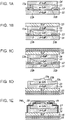
- a mask 12 made of Si02 is formed on the upper surface of a GaN layer which is a surface layer of a substrate 11 illustrated in Fig. 1A .
- the lower surface of the GaN layer which is the surface layer of the substrate 11 may be supported by a component, such as a silicon substrate (not illustrated), other than GaN.
- the component may be, for example, a sapphire substrate or a SiC (silicon carbide) substrate.
- Another material such as SiN, AlN, Al2O3, or Ga2O3 may be used as the material of the mask 12.
- the mask 12 may be amorphous.
- the mask 12 has an opening 12a.
- a peripheral upper surface region of the opening 12a is subjected to a region selection due to a shape.
- the region selection is due to a shape having a difference in level 12b and is a selection for dividing a region into an upper side and a lower side of the difference in level.
- the difference in level 12b surrounds the entire periphery of the opening 12a, and a lower step is formed near the opening 12a and an upper step is formed in a region away from the opening 12a. That is, the boundary line between the regions divided by the region selection surrounds the opening 12a.
- Such a shape with the difference in level 12b is formed by, for example, a well-known photolithography technique and wet etching or dry etching.
- GaN is epitaxially grown from the surface of the substrate 11 exposed from the opening 12a to the top of the peripheral upper surface region by the ELO technique described above to form a GaN layer 13.
- the GaN layer 13 since the GaN layer 13 is grown to the top of the peripheral upper surface region that has been subjected to the region selection, the GaN layer 13 extends to different regions that have been subjected to the region selection.
- the different regions that have been subjected to the region selection are the lower step and the upper step with respect to the difference in level 12b. Accordingly, the GaN layer 13 extends not only to the lower step but also to the upper step.
- the effect of the region selection in this embodiment is the transfer of the shape to a semiconductor layer.
- the doping amount of an n-type impurity is controlled such that the GaN layer 13 has an electron carrier concentration of less than 10 17 cm -3 .
- the n-type impurity may be, for example, Si (silicon). This enables the formation of a voltage withstanding layer in which a depletion layer spreads when a voltage is applied during the operation of the device.
- a GaN layer 14 having a high impurity concentration is epitaxially grown so as to cover the GaN layer 13, thereby forming the state illustrated in Fig. 1A .
- a semiconductor element having a semiconductor layer (GaN layer 13) in which the effect of the region selection on the upper surface of the mask 12 remains is fabricated.
- a surface of a semiconductor layer (upper surface of the GaN layer 14) opposite to the substrate 11 is joined to a support substrate 15.
- a joining via a metal or a direct joining may be used as the joining to reduce the resistance of the connection.
- a back-surface electrode 16 is formed on the upper surface of the support substrate 15 by, for example, sputtering.
- the back-surface electrode 16 is, for example, an Al layer plated with Ti, Ni, and Au.
- the back-surface electrode may be formed after an upper-surface-electrode metal film 19 described later is formed.
- a support substrate 15 on which a back-surface electrode 16 is provided in advance may be used.
- the support substrate 15 may be formed of a semiconductor having a high impurity concentration so as to achieve a low resistance.
- the semiconductor layers 13 and 14 are separated from the substrate 11 in the state where the surface of the semiconductor layer (upper surface of the GaN layer 14) is joined to the support substrate 15.
- the mask 12 is previously dissolved by wet etching, dry etching, or the like, and cracks are then formed in crystals near the opening 12a by, for example, ultrasonic waves to perform stripping from the substrate 11.
- a step 13b is formed around the surface 13a at a position one step lower from the surface 13a
- a step 13c is formed around the step 13b at a position one step lower from the step 13b.
- a difference in level 13b-13c is used as a mesa structure.
- an insulating film 17 that has an opening surrounding the surface 13a and that covers the mesa structure (13b-13c) is formed.
- a Schottky metal film 18 that is joined to the GaN layer 13 exposed in the opening of the insulating film 17 by Schottky junction is formed.
- the opening of the insulating film 17 is covered with the Schottky metal film 18.
- an upper-surface-electrode metal film 19 extending to the mesa structure (13b-13c) is formed on the Schottky metal film 18 and on the insulating film 17.
- the upper-surface-electrode metal film 19 forms the so-called field plate on the insulating film 17.
- the semiconductor element 100 is a Schottky barrier diode.
- the mesa structure is formed in the semiconductor element 100 by transferring the shape of the mask 12.
- the shape is not limited to the embodiment described above and may have a difference in level at two or more positions.
- a protruding shape can also be formed by forming a shape that ascends upward once and descends downward.
- a trench structure can also be formed by transferring such a protruding shape of the mask 12.
- the mesa structure may be a trench structure.
- one or a plurality of trench structures and a mesa structure at the outermost edge can be formed from the center of the semiconductor element 100 toward the periphery thereof.
- the shape may be a step with an inclination or a structure with a rounded corner.
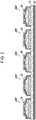
- the manufacturing process described above is simultaneously performed in parallel so as to manufacture a plurality of semiconductor elements 100 at the same time, as illustrated in Fig. 2 .
- a plurality of openings 12a is formed in the mask 12, and a plurality of semiconductor elements is fabricated at the same time so that one semiconductor element corresponds to one opening.
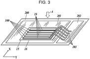
- the semiconductor elements 100 can be separated into pieces and individually used as a semiconductor device. However, if it is necessary to increase the capacity, while the support substrate 15 and the back-surface electrode 16 are shared by the plurality of semiconductor elements 100 as illustrated in Fig. 2 , the semiconductor elements 100 can be mounted and used as a semiconductor device, as illustrated in Fig. 3 .
- the common back-surface electrode 16 is die-bonded to one electrode pad 201 on a mounting substrate 200, and upper-surface-electrode metal films 19 are each connected to another electrode pad 202 through bonding wires 203.
- the manufacturing is performed such that the plurality of semiconductor elements 100 is arranged side by side in one direction X.
- the semiconductor elements 100 each have, in plan view (as viewed in the direction of arrow A), a shape that is long in a direction Y substantially orthogonal to the direction X in which the semiconductor elements 100 are arranged. Such a shape and an arrangement easily increase the junction area of the diodes.
- the opening 12a of the mask 12 in the manufacturing process has a substantially rectangular shape in plan view perpendicular to the substrate 11.
- the long-side direction of this rectangle is a direction perpendicular to the drawing in Fig. 2 .
- the semiconductor layers 13 and 14 and the semiconductor element 100 that mainly includes the semiconductor layers 13 and 14 each have a substantially rectangular shape having a long-side direction (Y) in the long-side direction of the opening 12a of the mask 12 in plan view.
- a region selection on a mask 12 is due to a predetermined element that is selectively arranged, and the effect of the region selection on a semiconductor layer is diffusion of the element into the semiconductor layer.
- an element is arranged for a mask 12 instead of the difference in level of the first embodiment.
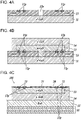
- a P-type impurity 12p is arranged.
- the method for arranging the P-type impurity 12p is not particularly limited and may be a method in which the P-type impurity 12p is introduced into the mask 12, as illustrated in Fig. 4A . Sputtering, thermal diffusion, or the like can be used for the introduction method. This gives a region selection, that is, a region selection for division into regions in which the P-type impurity 12p is arranged and other regions.
- a compound including a P-type impurity (a compound including a substance to be diffused into a semiconductor layer 13) may be arranged for the mask 12.
- the region may be previously formed in such a manner that the compound is arranged to be embedded so as not to affect the outer shape of the mask 12, or the compound may be arranged on the mask 12. If a shape having a difference in level on the upper surface of the mask 12 is formed, a region selection due to the shape and a region selection due to the substance are given at the same time. That is, a mask 12 that has been subjected to region selections due to the shape and the substance is provided.
- the P-type impurity 12p is arranged in a ring shape surrounding an opening 12a.
- GaN layers 13 and 14 are formed by epitaxial growth as in the first embodiment ( Fig. 4B ).
- part of the P-type impurity 12p moves into the GaN layer 13 and diffuses into the GaN layer 13 to form P-type regions 13p in the GaN layer 13.
- the diffusion of the P-type impurity 12p may be naturally performed in a high-temperature state during epitaxial growth of the GaN layers 13 and 14, or a heating step of diffusing the P-type impurity 12p may be further separately provided.
- a support substrate 15 and the formation of a back-surface electrode 16 are also similarly performed, and an insulating film 20 having openings is then formed on the surface of the GaN layer 13, as illustrated in Fig. 4C . Furthermore, through the openings of the insulating film 20, a Schottky metal film 21 that is joined to the N-type region of the GaN layer 13 by Schottky junction and metal rings 22 that are joined to the P-type regions 13p by ohmic junction are formed so that the metal rings 22 function as guard rings.
- a Schottky barrier diode 101 with guard rings can be manufactured. Details described with reference to Figs. 2 and 3 can be similarly carried out.
- the second embodiment is partially changed, and a semiconductor element 102 in which a PN junction and a Schottky junction coexist is manufactured.
- a manufacturing process similar to that of the second embodiment is performed.
- the number of lines of the P-type impurity 12p and the arrangement thereof are freely selected.
- the upper-surface-electrode metal film 30 is joined to P-type regions 13p and N-type regions of the GaN layer 13. Specifically, the upper-surface-electrode metal film 30 that is joined to the P-type regions 13p by ohmic junction and is joined to the N-type regions adjacent to the P-type regions 13p by Schottky junction is formed.
- the semiconductor element 102 in which a PN junction and a Schottky junction coexist can be manufactured. Details described with reference to Figs. 2 and 3 can be similarly carried out.
- a structure due to the effect of a region selection on the mask 12 can be formed on a surface of the semiconductor layers 13 and 14 that are epitaxially grown on the mask 12, the surface being in contact with the upper surface of the mask 12. Furthermore, by separating the semiconductor layers 13 and 14 from the substrate 11 and placing the resulting element such that the structure is located on the upper surface side of the element, a base of a high withstand voltage structure such as a mesa step, a field plate, or a guard ring can be provided.
- various structures other than the structures presented as examples may be formed by appropriately combining the first embodiment, the second embodiment, and the third embodiment.
- an N-type impurity may be diffused into the GaN layer instead of the P-type impurity.
- the region selection on the mask is not limited as long as the mask is physically or chemically subjected to a region selection due to a macroscopic or microscopic change in the structure, and the region selection leaves, so as to correspond to regions divided by the selection (sorting), different effects on epitaxial films that are grown on the regions.
- the region selection due to the shape can be achieved by a change in the inclination or a change in the surface roughness, and the shape is transferred. Even in the case of the same substance, a region selection may be achieved by a difference in the crystal structure or crystal orientation.
- the present disclosure is applicable to a method for manufacturing a semiconductor element, and a semiconductor device.
Landscapes
- Electrodes Of Semiconductors (AREA)
Abstract
Description
- The present disclosure relates to a method for manufacturing a semiconductor element, and a semiconductor device.
- There is a known technique called ELO (epitaxial lateral overgrowth) in which a GaN (gallium nitride) layer is formed by crystal growth in an opening of a growth mask provided on a substrate, and the crystals are further grown on the growth mask in the lateral direction (
Japanese Patent No. 4638958 - A method for manufacturing a semiconductor element according to one aspect of the present disclosure includes providing, on a surface of a substrate, a mask which has an opening and in which a peripheral upper surface region of the opening is processed to have a predetermined structure, and epitaxially growing a semiconductor from the surface of the substrate exposed from the opening to the top of the peripheral upper surface region to fabricate a semiconductor element having a semiconductor layer with the predetermined structure transferred thereon.
-
- [
Fig. 1A] Fig. 1A is a schematic sectional view for describing a first embodiment of the present disclosure. - [
Fig. 1B] Fig. 1B is a schematic sectional view for describing the first embodiment of the present disclosure. - [
Fig. 1C] Fig. 1C is a schematic sectional view for describing the first embodiment of the present disclosure. - [
Fig. 1D] Fig. 1D is a schematic sectional view for describing the first embodiment of the present disclosure. - [
Fig. 1E] Fig. 1E is a schematic sectional view for describing the first embodiment of the present disclosure. - [
Fig. 2] Fig. 2 is a schematic sectional view for describing the first embodiment of the present disclosure. - [
Fig. 3] Fig. 3 is a schematic perspective view for describing the first embodiment of the present disclosure. - [
Fig. 4A] Fig. 4A is a schematic sectional view for describing a second embodiment of the present disclosure. - [
Fig. 4B] Fig. 4B is a schematic sectional view for describing the second embodiment of the present disclosure. - [
Fig. 4C] Fig. 4C is a schematic sectional view for describing the second embodiment of the present disclosure. - [
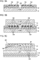
Fig. 5A] Fig. 5A is a schematic sectional view for describing a third embodiment of the present disclosure. - [
Fig. 5B] Fig. 5B is a schematic sectional view for describing the third embodiment of the present disclosure. - [
Fig. 5C] Fig. 5C is a schematic sectional view for describing the third embodiment of the present disclosure. Description of Embodiments - An embodiment of the present disclosure will be described below with reference to the drawings.
- First, a method for manufacturing a semiconductor element, and a semiconductor device of a first embodiment will be described.
- A semiconductor element is manufactured as follows.
- A
mask 12 made of Si02 is formed on the upper surface of a GaN layer which is a surface layer of asubstrate 11 illustrated inFig. 1A . The lower surface of the GaN layer which is the surface layer of thesubstrate 11 may be supported by a component, such as a silicon substrate (not illustrated), other than GaN. The component may be, for example, a sapphire substrate or a SiC (silicon carbide) substrate. Another material such as SiN, AlN, Al2O3, or Ga2O3 may be used as the material of themask 12. Themask 12 may be amorphous. - The
mask 12 has an opening 12a. In this embodiment, a peripheral upper surface region of the opening 12a is subjected to a region selection due to a shape. The region selection is due to a shape having a difference inlevel 12b and is a selection for dividing a region into an upper side and a lower side of the difference in level. The difference inlevel 12b surrounds the entire periphery of the opening 12a, and a lower step is formed near the opening 12a and an upper step is formed in a region away from the opening 12a. That is, the boundary line between the regions divided by the region selection surrounds the opening 12a. Such a shape with the difference inlevel 12b is formed by, for example, a well-known photolithography technique and wet etching or dry etching. - Next, GaN is epitaxially grown from the surface of the
substrate 11 exposed from the opening 12a to the top of the peripheral upper surface region by the ELO technique described above to form aGaN layer 13. In this case, since the GaNlayer 13 is grown to the top of the peripheral upper surface region that has been subjected to the region selection, theGaN layer 13 extends to different regions that have been subjected to the region selection. In this embodiment, the different regions that have been subjected to the region selection are the lower step and the upper step with respect to the difference inlevel 12b. Accordingly, the GaNlayer 13 extends not only to the lower step but also to the upper step. - As a result, a stepped shape is transferred to the lower surface of the
GaN layer 13. Thus, the effect of the region selection in this embodiment is the transfer of the shape to a semiconductor layer. - The doping amount of an n-type impurity is controlled such that the
GaN layer 13 has an electron carrier concentration of less than 1017 cm-3. The n-type impurity may be, for example, Si (silicon). This enables the formation of a voltage withstanding layer in which a depletion layer spreads when a voltage is applied during the operation of the device. - Furthermore, in this embodiment, in order to obtain a desired impurity concentration profile, a
GaN layer 14 having a high impurity concentration is epitaxially grown so as to cover theGaN layer 13, thereby forming the state illustrated inFig. 1A . - As described above, a semiconductor element having a semiconductor layer (GaN layer 13) in which the effect of the region selection on the upper surface of the
mask 12 remains is fabricated. - Next, as illustrated in
Fig. 1B , a surface of a semiconductor layer (upper surface of the GaN layer 14) opposite to thesubstrate 11 is joined to asupport substrate 15. A joining via a metal or a direct joining may be used as the joining to reduce the resistance of the connection. - Next, as illustrated in
Fig. 1C , a back-surface electrode 16 is formed on the upper surface of thesupport substrate 15 by, for example, sputtering. The back-surface electrode 16 is, for example, an Al layer plated with Ti, Ni, and Au. - The back-surface electrode may be formed after an upper-surface-
electrode metal film 19 described later is formed. Alternatively, asupport substrate 15 on which a back-surface electrode 16 is provided in advance may be used. Thesupport substrate 15 may be formed of a semiconductor having a high impurity concentration so as to achieve a low resistance. - Next, the semiconductor layers 13 and 14 are separated from the
substrate 11 in the state where the surface of the semiconductor layer (upper surface of the GaN layer 14) is joined to thesupport substrate 15. Themask 12 is previously dissolved by wet etching, dry etching, or the like, and cracks are then formed in crystals near theopening 12a by, for example, ultrasonic waves to perform stripping from thesubstrate 11. - After the separation, the resulting product is turned upside down to form the state illustrated in
Fig. 1D . - As illustrated in
Fig. 1D , with respect to asurface 13a of thesemiconductor layer 13 separated from thesubstrate 11, astep 13b is formed around thesurface 13a at a position one step lower from thesurface 13a, and astep 13c is formed around thestep 13b at a position one step lower from thestep 13b. A difference inlevel 13b-13c is used as a mesa structure. - Next, an insulating
film 17 that has an opening surrounding thesurface 13a and that covers the mesa structure (13b-13c) is formed. Next, a Schottky metal film 18 that is joined to theGaN layer 13 exposed in the opening of the insulatingfilm 17 by Schottky junction is formed. The opening of the insulatingfilm 17 is covered with the Schottky metal film 18. - Next, an upper-surface-
electrode metal film 19 extending to the mesa structure (13b-13c) is formed on the Schottky metal film 18 and on the insulatingfilm 17. The upper-surface-electrode metal film 19 forms the so-called field plate on the insulatingfilm 17. - Thus, a
semiconductor element 100 is manufactured. Here, thesemiconductor element 100 is a Schottky barrier diode. - As described above, the mesa structure is formed in the
semiconductor element 100 by transferring the shape of themask 12. - The shape is not limited to the embodiment described above and may have a difference in level at two or more positions. In
Fig. 1A , not only a difference in level ascending from theopening 12a toward the periphery but also a difference in level descending downward can be carried out. Accordingly, a protruding shape can also be formed by forming a shape that ascends upward once and descends downward. A trench structure can also be formed by transferring such a protruding shape of themask 12. Accordingly, the mesa structure may be a trench structure. Alternatively, one or a plurality of trench structures and a mesa structure at the outermost edge can be formed from the center of thesemiconductor element 100 toward the periphery thereof. - The shape may be a step with an inclination or a structure with a rounded corner.
- The manufacturing process described above is simultaneously performed in parallel so as to manufacture a plurality of
semiconductor elements 100 at the same time, as illustrated inFig. 2 . Specifically, a plurality ofopenings 12a is formed in themask 12, and a plurality of semiconductor elements is fabricated at the same time so that one semiconductor element corresponds to one opening. - The
semiconductor elements 100 can be separated into pieces and individually used as a semiconductor device. However, if it is necessary to increase the capacity, while thesupport substrate 15 and the back-surface electrode 16 are shared by the plurality ofsemiconductor elements 100 as illustrated inFig. 2 , thesemiconductor elements 100 can be mounted and used as a semiconductor device, as illustrated inFig. 3 . - As illustrated in
Fig. 3 , the common back-surface electrode 16 is die-bonded to oneelectrode pad 201 on a mountingsubstrate 200, and upper-surface-electrode metal films 19 are each connected to anotherelectrode pad 202 throughbonding wires 203. - Mounting in this manner enables a plurality of diodes to be connected in parallel and to be used in a large capacity. In this case, the manufacturing is performed such that the plurality of
semiconductor elements 100 is arranged side by side in one direction X. Thesemiconductor elements 100 each have, in plan view (as viewed in the direction of arrow A), a shape that is long in a direction Y substantially orthogonal to the direction X in which thesemiconductor elements 100 are arranged. Such a shape and an arrangement easily increase the junction area of the diodes. - For this purpose, the
opening 12a of themask 12 in the manufacturing process has a substantially rectangular shape in plan view perpendicular to thesubstrate 11. The long-side direction of this rectangle is a direction perpendicular to the drawing inFig. 2 . As a result of epitaxial growth from the substantiallyrectangular opening 12a, the semiconductor layers 13 and 14 and thesemiconductor element 100 that mainly includes the semiconductor layers 13 and 14 each have a substantially rectangular shape having a long-side direction (Y) in the long-side direction of theopening 12a of themask 12 in plan view. - Next, a second embodiment which is another embodiment will be described.
- In this embodiment, a region selection on a
mask 12 is due to a predetermined element that is selectively arranged, and the effect of the region selection on a semiconductor layer is diffusion of the element into the semiconductor layer. - As illustrated in
Fig. 4A , an element is arranged for amask 12 instead of the difference in level of the first embodiment. Here, a P-type impurity 12p is arranged. The method for arranging the P-type impurity 12p is not particularly limited and may be a method in which the P-type impurity 12p is introduced into themask 12, as illustrated inFig. 4A . Sputtering, thermal diffusion, or the like can be used for the introduction method. This gives a region selection, that is, a region selection for division into regions in which the P-type impurity 12p is arranged and other regions. - Alternatively, a compound including a P-type impurity (a compound including a substance to be diffused into a semiconductor layer 13) may be arranged for the
mask 12. Regarding the arrangement position, the region may be previously formed in such a manner that the compound is arranged to be embedded so as not to affect the outer shape of themask 12, or the compound may be arranged on themask 12. If a shape having a difference in level on the upper surface of themask 12 is formed, a region selection due to the shape and a region selection due to the substance are given at the same time. That is, amask 12 that has been subjected to region selections due to the shape and the substance is provided. The P-type impurity 12p is arranged in a ring shape surrounding anopening 12a. - After the
mask 12 is subjected to the region selection due to an element, GaN layers 13 and 14 are formed by epitaxial growth as in the first embodiment (Fig. 4B ). - Consequently, part of the P-
type impurity 12p moves into theGaN layer 13 and diffuses into theGaN layer 13 to form P-type regions 13p in theGaN layer 13. In this case, the diffusion of the P-type impurity 12p may be naturally performed in a high-temperature state during epitaxial growth of the GaN layers 13 and 14, or a heating step of diffusing the P-type impurity 12p may be further separately provided. - The joining of a
support substrate 15 and the formation of a back-surface electrode 16 are also similarly performed, and an insulatingfilm 20 having openings is then formed on the surface of theGaN layer 13, as illustrated inFig. 4C . Furthermore, through the openings of the insulatingfilm 20, aSchottky metal film 21 that is joined to the N-type region of theGaN layer 13 by Schottky junction and metal rings 22 that are joined to the P-type regions 13p by ohmic junction are formed so that the metal rings 22 function as guard rings. - Thus, a
Schottky barrier diode 101 with guard rings can be manufactured. Details described with reference toFigs. 2 and3 can be similarly carried out. - A third embodiment which is still another embodiment will be described.
- In this embodiment, the second embodiment is partially changed, and a
semiconductor element 102 in which a PN junction and a Schottky junction coexist is manufactured. - As illustrated in
Figs. 5A and 5B , a manufacturing process similar to that of the second embodiment is performed. The number of lines of the P-type impurity 12p and the arrangement thereof are freely selected. - As illustrated in
Fig. 5C , the separation from asubstrate 11 and amask 12 and the formation of a back-surface electrode 16 are completed, and an upper-surface-electrode metal film 30 is formed on the surface of aGaN layer 13. - The upper-surface-
electrode metal film 30 is joined to P-type regions 13p and N-type regions of theGaN layer 13. Specifically, the upper-surface-electrode metal film 30 that is joined to the P-type regions 13p by ohmic junction and is joined to the N-type regions adjacent to the P-type regions 13p by Schottky junction is formed. - Thus, the
semiconductor element 102 in which a PN junction and a Schottky junction coexist can be manufactured. Details described with reference toFigs. 2 and3 can be similarly carried out. - According to the above embodiments of the present disclosure, a structure due to the effect of a region selection on the
mask 12 can be formed on a surface of the semiconductor layers 13 and 14 that are epitaxially grown on themask 12, the surface being in contact with the upper surface of themask 12. Furthermore, by separating the semiconductor layers 13 and 14 from thesubstrate 11 and placing the resulting element such that the structure is located on the upper surface side of the element, a base of a high withstand voltage structure such as a mesa step, a field plate, or a guard ring can be provided. - Although embodiments of the present disclosure have been described above, these embodiments are presented as examples and can be carried out in other various forms, and omissions, replacements, and changes are possible within the range that does not depart from the gist of the invention.
- For example, various structures other than the structures presented as examples may be formed by appropriately combining the first embodiment, the second embodiment, and the third embodiment.
- For example, in the second embodiment and the third embodiment, an N-type impurity may be diffused into the GaN layer instead of the P-type impurity.
- In the embodiments described above, a region selection due to the shape and a region selection due to the arrangement of a substance have been described. However, the region selection on the mask is not limited as long as the mask is physically or chemically subjected to a region selection due to a macroscopic or microscopic change in the structure, and the region selection leaves, so as to correspond to regions divided by the selection (sorting), different effects on epitaxial films that are grown on the regions.
- The region selection due to the shape can be achieved by a change in the inclination or a change in the surface roughness, and the shape is transferred. Even in the case of the same substance, a region selection may be achieved by a difference in the crystal structure or crystal orientation.
- The present disclosure is applicable to a method for manufacturing a semiconductor element, and a semiconductor device.
-
- 11
- substrate
- 12
- mask
- 12a
- opening of mask
- 12b
- difference in level
- 12p
- P-type impurity
- 13
- GaN layer (semiconductor layer)
- 13p
- P-type region
- 14
- GaN layer (semiconductor layer)
- 15
- support substrate
- 16
- back-surface electrode
- 17
- insulating film
- 18
- Schottky metal film
- 19
- upper-surface-electrode metal film
- 20
- insulating film
- 21
- Schottky metal film
- 22
- metal ring (guard ring)
- 30
- upper-surface-electrode metal film
- 100
- semiconductor element (diode)
- 200
- mounting substrate
- 201
- electrode pad
- 202
- electrode pad
- 203
- bonding wire
Claims (14)
- A method for manufacturing a semiconductor element, comprising:providing, on a surface of a substrate, a mask which has an opening and in which a peripheral upper surface region of the opening is processed to have a predetermined structure; andepitaxially growing a semiconductor from the surface of the substrate exposed from the opening to the top of the peripheral upper surface region to fabricate a semiconductor element having a semiconductor layer with the predetermined structure transferred thereon.
- The method for manufacturing a semiconductor element according to claim 1, wherein the predetermined structure is a shape having a difference in level.
- The method for manufacturing a semiconductor element according to claim 2, wherein a mesa structure or a trench structure is formed in the semiconductor element by transferring the shape.
- The method for manufacturing a semiconductor element according to any one of claims 1 to 3, wherein the processed region surrounds the opening.
- The method for manufacturing a semiconductor element according to claim 3, comprising:removing the mask;separating the semiconductor layer from the substrate in a state where a surface of the semiconductor layer opposite to the substrate is joined to a support substrate;subsequently forming an insulating film that has an opening surrounding a surface of the semiconductor layer separated from the substrate and that covers the mesa structure or the trench structure; andsubsequently covering the opening of the insulating film and forming, on the insulating film, a metal film extending to the mesa structure or the trench structure.
- The method for manufacturing a semiconductor element according to claim 1,wherein the predetermined structure is formed by selectively arranging a predetermined element for the mask, andthe element is moved into the semiconductor layer by the transfer.
- The method for manufacturing a semiconductor element according to claim 1 or 6, wherein the predetermined element is arranged for the mask by introducing the predetermined element into the mask.
- The method for manufacturing a semiconductor element according to claim 1 or 6, wherein the predetermined element is arranged for the mask by arranging a compound including the predetermined element.
- The method for manufacturing a semiconductor element according to claim 6 or 7, wherein the processed region surrounds the opening.
- The method for manufacturing a semiconductor element according to claim 9, comprising:epitaxially growing the semiconductor to be of N-type;diffusing a P-type impurity as the element into the semiconductor layer to form a P-type region in the semiconductor layer;subsequently removing the mask;separating the semiconductor layer from the substrate in a state where a surface of the semiconductor layer opposite to the substrate is joined to a support substrate; andsubsequently forming a metal ring joined to the P-type region to function as a guard ring.
- The method for manufacturing a semiconductor element according to claim 9, comprising:epitaxially growing the semiconductor to be of N-type;diffusing a P-type impurity as the substance into the semiconductor layer to form a P-type region in the semiconductor layer;subsequently removing the mask;separating the semiconductor layer from the substrate in a state where a surface of the semiconductor layer opposite to the substrate is joined to a support substrate; andsubsequently forming a metal film that is joined to the P-type region by ohmic junction and that is joined to the N-type region adjacent to the P-type region by Schottky junction.
- The method for manufacturing a semiconductor element according to any one of claims 1 to 11,wherein the opening of the mask has a substantially rectangular shape in plan view, andthe semiconductor layer has a substantially rectangular shape having a long-side direction in a long-side direction of the opening of the mask in plan view.
- The method for manufacturing a semiconductor element according to any one of claims 1 to 12, wherein a plurality of openings is formed in the mask, and a plurality of semiconductor elements is fabricated at the same time so that one semiconductor element corresponds to one opening.
- A semiconductor device comprising a semiconductor element manufactured by the method for manufacturing a semiconductor element according to any one of claims 1 to 13.
Applications Claiming Priority (2)
| Application Number | Priority Date | Filing Date | Title |
|---|---|---|---|
| JP2019178961 | 2019-09-30 | ||
| PCT/JP2020/036647 WO2021065803A1 (en) | 2019-09-30 | 2020-09-28 | Method for manufacturing semiconductor element, and semiconductor device |
Publications (1)
| Publication Number | Publication Date |
|---|---|
| EP4040468A1 true EP4040468A1 (en) | 2022-08-10 |
Family
ID=75338232
Family Applications (1)
| Application Number | Title | Priority Date | Filing Date |
|---|---|---|---|
| EP20872323.9A Withdrawn EP4040468A1 (en) | 2019-09-30 | 2020-09-28 | Method for manufacturing semiconductor element, and semiconductor device |
Country Status (5)
| Country | Link |
|---|---|
| US (1) | US20220359196A1 (en) |
| EP (1) | EP4040468A1 (en) |
| JP (1) | JPWO2021065803A1 (en) |
| CN (1) | CN114402422A (en) |
| WO (1) | WO2021065803A1 (en) |
Families Citing this family (2)
| Publication number | Priority date | Publication date | Assignee | Title |
|---|---|---|---|---|
| US20230197446A1 (en) * | 2020-04-27 | 2023-06-22 | Kyocera Corporation | Manufacturing method for semiconductor element, and semiconductor device |
| CN116508137A (en) * | 2020-10-28 | 2023-07-28 | 加利福尼亚大学董事会 | Method for transferring patterns to epitaxial layers of light emitting devices |
Family Cites Families (10)
| Publication number | Priority date | Publication date | Assignee | Title |
|---|---|---|---|---|
| JPS4638958B1 (en) | 1962-03-20 | 1971-11-16 | ||
| JP2001010898A (en) * | 1999-06-24 | 2001-01-16 | Nec Corp | Crystal substrate and its production |
| US20050186757A1 (en) * | 2004-02-20 | 2005-08-25 | National Chiao Tung University | Method for lift off GaN pseudomask epitaxy layer using wafer bonding way |
| US20060292719A1 (en) * | 2005-05-17 | 2006-12-28 | Amberwave Systems Corporation | Lattice-mismatched semiconductor structures with reduced dislocation defect densities and related methods for device fabrication |
| JP4638958B1 (en) * | 2009-08-20 | 2011-02-23 | 株式会社パウデック | Manufacturing method of semiconductor device |
| WO2012066804A1 (en) * | 2010-11-19 | 2012-05-24 | 京セラ株式会社 | Method for manufacturing semiconductor substrate, and light emitting element |
| TWI627303B (en) * | 2011-11-04 | 2018-06-21 | Asm國際股份有限公司 | Method for depositing doped silicon oxide on substrate in reaction chamber |
| KR101363611B1 (en) * | 2012-04-30 | 2014-02-19 | 부경대학교 산학협력단 | Compound Semiconductor With Selective Sputtered Film And Manufacturing Method Thereof |
| JP2014049616A (en) * | 2012-08-31 | 2014-03-17 | Sony Corp | Diode and manufacturing method of diode |
| CN111919281B (en) * | 2018-02-12 | 2024-04-02 | 克罗米斯有限公司 | Method and system for forming doped regions in gallium nitride material by diffusion |
-
2020
- 2020-09-28 WO PCT/JP2020/036647 patent/WO2021065803A1/en not_active Ceased
- 2020-09-28 JP JP2021551254A patent/JPWO2021065803A1/ja active Pending
- 2020-09-28 CN CN202080059243.6A patent/CN114402422A/en active Pending
- 2020-09-28 US US17/763,043 patent/US20220359196A1/en not_active Abandoned
- 2020-09-28 EP EP20872323.9A patent/EP4040468A1/en not_active Withdrawn
Also Published As
| Publication number | Publication date |
|---|---|
| JPWO2021065803A1 (en) | 2021-04-08 |
| CN114402422A (en) | 2022-04-26 |
| WO2021065803A1 (en) | 2021-04-08 |
| US20220359196A1 (en) | 2022-11-10 |
Similar Documents
| Publication | Publication Date | Title |
|---|---|---|
| US9608100B2 (en) | High electron mobility transistor and method of manufacturing the same | |
| US11417778B2 (en) | Semiconductor MPS diode with reduced current-crowding effect and manufacturing method thereof | |
| US8956960B2 (en) | Method for stress reduced manufacturing semiconductor devices | |
| EP3300100B1 (en) | Semiconductor wafer and method for fabricating a semiconductor wafer | |
| EP3608972B1 (en) | Semiconductor device | |
| EP4040468A1 (en) | Method for manufacturing semiconductor element, and semiconductor device | |
| CN103681879B (en) | Diode and the method for manufacturing diode | |
| CN102479705B (en) | Semiconductor device and the method be used for producing the semiconductor devices | |
| CN113394281A (en) | GaN-based HEMT device based on substrate conductive hole and preparation method thereof | |
| JP7113554B2 (en) | Semiconductor device manufacturing method and semiconductor substrate | |
| US12283534B2 (en) | Power semiconductor devices with improved overcoat adhesion and/or protection | |
| US12113127B2 (en) | GaN-based high electron mobility transistors and fabrication method thereof | |
| US20230030874A1 (en) | Semiconductor element, method for manufacturing semiconductor element, semiconductor device, and method for manufacturing semiconductor device | |
| US9735290B2 (en) | Semiconductor device | |
| CN120826994A (en) | Junction Barrier Schottky Diode | |
| CN115443544A (en) | Manufacturing method of semiconductor element and semiconductor device | |
| TWI893614B (en) | Schottky barrier diode | |
| WO2022025080A1 (en) | Manufacturing method for semiconductor element, semiconductor element and semiconductor device | |
| US20250194191A1 (en) | Power Semiconductor Devices | |
| US20260053057A1 (en) | Encapsulation delamination prevention structures at die edge | |
| EP4040484A1 (en) | Method for manufacturing semiconductor device and semiconductor device | |
| US11764110B2 (en) | Moat coverage with dielectric film for device passivation and singulation | |
| WO2022091803A1 (en) | Method for producing semiconductor element, semiconductor element, and semiconductor device | |
| CN114846589A (en) | Method for manufacturing semiconductor element and semiconductor device | |
| WO2022131059A1 (en) | Method for manufacturing semiconductor element, semiconductor element, and semiconductor device |
Legal Events
| Date | Code | Title | Description |
|---|---|---|---|
| STAA | Information on the status of an ep patent application or granted ep patent |
Free format text: STATUS: THE INTERNATIONAL PUBLICATION HAS BEEN MADE |
|
| PUAI | Public reference made under article 153(3) epc to a published international application that has entered the european phase |
Free format text: ORIGINAL CODE: 0009012 |
|
| STAA | Information on the status of an ep patent application or granted ep patent |
Free format text: STATUS: REQUEST FOR EXAMINATION WAS MADE |
|
| 17P | Request for examination filed |
Effective date: 20220311 |
|
| AK | Designated contracting states |
Kind code of ref document: A1 Designated state(s): AL AT BE BG CH CY CZ DE DK EE ES FI FR GB GR HR HU IE IS IT LI LT LU LV MC MK MT NL NO PL PT RO RS SE SI SK SM TR |
|
| DAV | Request for validation of the european patent (deleted) | ||
| DAX | Request for extension of the european patent (deleted) | ||
| P01 | Opt-out of the competence of the unified patent court (upc) registered |
Effective date: 20230505 |
|
| STAA | Information on the status of an ep patent application or granted ep patent |
Free format text: STATUS: THE APPLICATION HAS BEEN WITHDRAWN |
|
| 18W | Application withdrawn |
Effective date: 20230628 |