EP4037097A1 - Waveguide with lobe suppression - Google Patents
Waveguide with lobe suppression Download PDFInfo
- Publication number
- EP4037097A1 EP4037097A1 EP21212703.9A EP21212703A EP4037097A1 EP 4037097 A1 EP4037097 A1 EP 4037097A1 EP 21212703 A EP21212703 A EP 21212703A EP 4037097 A1 EP4037097 A1 EP 4037097A1
- Authority
- EP
- European Patent Office
- Prior art keywords
- waveguide
- pipe
- radiating slots
- parasitic
- parasitic groove
- Prior art date
- Legal status (The legal status is an assumption and is not a legal conclusion. Google has not performed a legal analysis and makes no representation as to the accuracy of the status listed.)
- Granted
Links
Images




Classifications
-
- H—ELECTRICITY
- H01—ELECTRIC ELEMENTS
- H01Q—ANTENNAS, i.e. RADIO AERIALS
- H01Q21/00—Antenna arrays or systems
- H01Q21/0006—Particular feeding systems
- H01Q21/0037—Particular feeding systems linear waveguide fed arrays
- H01Q21/0043—Slotted waveguides
-
- G—PHYSICS
- G01—MEASURING; TESTING
- G01S—RADIO DIRECTION-FINDING; RADIO NAVIGATION; DETERMINING DISTANCE OR VELOCITY BY USE OF RADIO WAVES; LOCATING OR PRESENCE-DETECTING BY USE OF THE REFLECTION OR RERADIATION OF RADIO WAVES; ANALOGOUS ARRANGEMENTS USING OTHER WAVES
- G01S7/00—Details of systems according to groups G01S13/00, G01S15/00, G01S17/00
- G01S7/02—Details of systems according to groups G01S13/00, G01S15/00, G01S17/00 of systems according to group G01S13/00
- G01S7/03—Details of HF subsystems specially adapted therefor, e.g. common to transmitter and receiver
-
- H—ELECTRICITY
- H01—ELECTRIC ELEMENTS
- H01Q—ANTENNAS, i.e. RADIO AERIALS
- H01Q13/00—Waveguide horns or mouths; Slot antennas; Leaky-waveguide antennas; Equivalent structures causing radiation along the transmission path of a guided wave
- H01Q13/20—Non-resonant leaky-waveguide or transmission-line antennas; Equivalent structures causing radiation along the transmission path of a guided wave
- H01Q13/22—Longitudinal slot in boundary wall of waveguide or transmission line
-
- B—PERFORMING OPERATIONS; TRANSPORTING
- B60—VEHICLES IN GENERAL
- B60R—VEHICLES, VEHICLE FITTINGS, OR VEHICLE PARTS, NOT OTHERWISE PROVIDED FOR
- B60R16/00—Electric or fluid circuits specially adapted for vehicles and not otherwise provided for; Arrangement of elements of electric or fluid circuits specially adapted for vehicles and not otherwise provided for
- B60R16/02—Electric or fluid circuits specially adapted for vehicles and not otherwise provided for; Arrangement of elements of electric or fluid circuits specially adapted for vehicles and not otherwise provided for electric constitutive elements
- B60R16/023—Electric or fluid circuits specially adapted for vehicles and not otherwise provided for; Arrangement of elements of electric or fluid circuits specially adapted for vehicles and not otherwise provided for electric constitutive elements for transmission of signals between vehicle parts or subsystems
-
- G—PHYSICS
- G01—MEASURING; TESTING
- G01S—RADIO DIRECTION-FINDING; RADIO NAVIGATION; DETERMINING DISTANCE OR VELOCITY BY USE OF RADIO WAVES; LOCATING OR PRESENCE-DETECTING BY USE OF THE REFLECTION OR RERADIATION OF RADIO WAVES; ANALOGOUS ARRANGEMENTS USING OTHER WAVES
- G01S13/00—Systems using the reflection or reradiation of radio waves, e.g. radar systems; Analogous systems using reflection or reradiation of waves whose nature or wavelength is irrelevant or unspecified
- G01S13/88—Radar or analogous systems specially adapted for specific applications
- G01S13/93—Radar or analogous systems specially adapted for specific applications for anti-collision purposes
- G01S13/931—Radar or analogous systems specially adapted for specific applications for anti-collision purposes of land vehicles
-
- H—ELECTRICITY
- H01—ELECTRIC ELEMENTS
- H01P—WAVEGUIDES; RESONATORS, LINES, OR OTHER DEVICES OF THE WAVEGUIDE TYPE
- H01P3/00—Waveguides; Transmission lines of the waveguide type
- H01P3/12—Hollow waveguides
- H01P3/122—Dielectric loaded (not air)
-
- H—ELECTRICITY
- H01—ELECTRIC ELEMENTS
- H01Q—ANTENNAS, i.e. RADIO AERIALS
- H01Q1/00—Details of, or arrangements associated with, antennas
- H01Q1/27—Adaptation for use in or on movable bodies
- H01Q1/32—Adaptation for use in or on road or rail vehicles
- H01Q1/3208—Adaptation for use in or on road or rail vehicles characterised by the application wherein the antenna is used
- H01Q1/3233—Adaptation for use in or on road or rail vehicles characterised by the application wherein the antenna is used particular used as part of a sensor or in a security system, e.g. for automotive radar, navigation systems
-
- H—ELECTRICITY
- H01—ELECTRIC ELEMENTS
- H01Q—ANTENNAS, i.e. RADIO AERIALS
- H01Q13/00—Waveguide horns or mouths; Slot antennas; Leaky-waveguide antennas; Equivalent structures causing radiation along the transmission path of a guided wave
- H01Q13/10—Resonant slot antennas
-
- H—ELECTRICITY
- H01—ELECTRIC ELEMENTS
- H01Q—ANTENNAS, i.e. RADIO AERIALS
- H01Q1/00—Details of, or arrangements associated with, antennas
- H01Q1/52—Means for reducing coupling between antennas; Means for reducing coupling between an antenna and another structure
- H01Q1/528—Means for reducing coupling between antennas; Means for reducing coupling between an antenna and another structure reducing the re-radiation of a support structure
Definitions
- Some devices use electromagnetic signals to detect and track objects.
- the electromagnetic signals are transmitted and received using one or more antennas.
- An antenna may be characterized in terms of gain, beam width, or, more specifically, pattern, which is a measure of the gain as a function of direction.
- a precisely controlled pattern may improve applications that require electromagnetic signals, and a waveguide may be used to improve such characteristics.
- the waveguide can include perforations or radiating slots that guide radiation near the antenna. Grating lobes, or secondary main lobes, may arise when the perforation spacing is greater than one-half wavelength of the transceiver signal.
- an apparatus may include a waveguide including a pipe for containing a dielectric, the pipe defining an open end to a longitudinal direction through the pipe, and further including an array of radiating slots through a surface of the pipe and in communication with the dielectric.
- the waveguide further including at least one parasitic groove separate from the pipe and with at least a portion of a length that is parallel to the array of radiating slots.
- a system may include a coupler, a transceiver operable upon actuation to interact with electromagnetic waves associated with the coupler, and a waveguide.
- the waveguide includes a pipe for capturing the electromagnetic waves and containing a dielectric, the pipe defining an open end to a longitudinal direction through the pipe.
- the waveguide further including an array of radiating slots through a surface of the pipe and in communication with the dielectric, and at least one parasitic groove separate from the pipe and with at least a portion of a length that is parallel to the array of radiating slots.
- the waveguide provides an antenna pattern where grating lobes are suppressed or substantially reduced.
- This document also describes other configurations and systems for providing lobe suppression.
- Radar systems are a sensing technology used in many industries (including the automotive industry) to acquire information about the surrounding environment.
- An antenna such as one described herein, may be employed in radar systems to transmit and receive electromagnetic energy or signals.
- Such a radar system may use multiple antenna-elements in an array to provide increased gain and directivity over what can be achieved using a single antenna-element.
- signals from the individual elements are combined with appropriate phases and weighted amplitudes to provide the desired antenna-reception pattern during reception.
- the antenna arrays are also used in transmission, splitting signal power amongst the elements and using appropriate phases and weighted amplitudes to provide the desired antenna transmission pattern.
- the waveguide can include an array of radiating slots.
- the radiating slots represent apertures of the waveguide, which may be arranged to provide desired phasing, combining, or splitting of signals and energy.
- the radiating slots which may also sometimes referred to as apertures, may be equally spaced in a surface of the waveguide, along a propagation direction of the electromagnetic waves.
- the radiating slots may cause grating lobes to appear in an antenna pattern. The size and shape of the grating lobes are based on the spacing and arrangement of the array of radiating slots.
- Reduced form factors may cause undesired grating lobe propagation according to ratios between radiating slot lengths, radiating slot spacing, wavelengths of the electromagnetic signal, and other organizational factors associated with the waveguide.
- the geometry of the waveguide may be adjusted, or the radiating slots may be rearranged in an attempt to reduce grating lobes below design specifications.
- the waveguide includes at least one parasitic groove that is separate from the pipe and with at least a portion of a length that is parallel to the array of radiating slots.
- the at least one parasitic groove has a uniform narrow width and uniform depth and is spaced apart from an array of radiating slots to achieve the desired lobe suppression.
- the parasitic groove is in a same surface of the waveguide, which defines the array of radiating slots.
- This parasitic groove may be defined according to various geometric shapes. As one example, the grooves may be linear and arranged in parallel to the radiating slots. In this way, the waveguide provides an antenna pattern where grating lobes are suppressed or substantially reduced.
- the example waveguide may be particularly advantageous for use in an automotive context, for example, detecting objects in a roadway.
- the grating lobes can indicate false detections within an automotive radar field-of-view. Suppressing these grating lobes improves accuracy of the radar as the number of false detections is reduced.
- the present disclosure describes lobe suppression with a waveguide. Indeed, such application of this and other examples provided in this disclosure increased radiation performance of a waveguide. These are but a few examples of how the described techniques and devices may be used to suppress grating lobes for multi-element waveguides.
- the document now turns to an example operating environment, after which example devices, methods, and systems are described.
- Fig. 1 illustrates an example system 100 that includes a waveguide 102 in accordance with techniques, apparatuses, and systems of this disclosure.
- the system 100 includes the waveguide 102, a coupler 108, a transceiver 110.
- the transceiver 110 may be operable upon actuation to interact with electromagnetic waves associated with the coupler 108 and the waveguide 102.
- the transceiver 110 may be a variety of components and may be a receiver or transmitter only.
- the coupler 108 is a link between the transceiver 110 and the waveguide 102 and may be a coaxial cable or another implement that connects through the open end 112 of the waveguide 102, forming an antenna assembly.
- the open end 112 may be opposite a closed end of the pipe 104.
- the open end 112 may define an opening such that the open end borders the dielectric 114 and defines an opening to a channel 116 through the pipe 104.
- the waveguide 102 includes a pipe 104.
- the pipe 104 may comprise various materials having various geometric shapes.
- the pipe 104 may be formed from metal to have a rectangular cross-section. Other non-exhaustive examples include cylindrical or square cross-sections.
- the pipe 104 includes an array of radiating slots 118 arranged on a surface 106 of the waveguide 102.
- the radiating slots 118 may be in communication with the dielectric 114, allowing electromagnetic waves propagated through the dielectric to bidirectionally flow through the radiating slots 118.
- the dielectric 114 may be any material. As an example, the dielectric 114 may be air from an environment surrounding the waveguide 102. Dielectric contained within the pipe 104 of the waveguide 102 may be reduced or removed to generate a vacuum volume defined by the waveguide 102.
- the waveguide 102 Separate from the pipe 104, the waveguide 102 includes a parasitic groove 120.
- the parasitic groove 120 may be implemented as various geometric shapes. In one example, the parasitic groove 120 may be linear and defined in parallel to the radiating slots 118.
- a second parasitic groove 122 of the waveguide 102 may be separate from the pipe 104.
- the second parasitic groove 122 may be similar to the parasitic groove 120 but on an opposite side of the radiating slots 118.
- the parasitic grooves 120, 122 may be defined anywhere on the pipe 104 and may be on a same side of the radiating slots 118 to achieve a particular suppression of grating lobes.
- the pipe 104 defines a longitudinal direction 128 and a latitudinal direction 126 perpendicular to the longitudinal direction 128.
- the parasitic grooves 120, 122 may be in parallel to the longitudinal direction 128.
- a propagation direction defined in the direction of electromagnetic waves traversing the pipe 104 and emanating from the coupler 108 may also be in parallel with the longitudinal direction 128. In this way, the parasitic grooves 120, 122 may be in parallel to the propagation direction of the electromagnetic waves that traverse the pipe 104.
- Fig. 2A illustrates a top-down view of an example waveguide 102-1 with lobe suppression, in accordance with one or more implementations of the present disclosure.
- the waveguide 102-1 shown in Fig. 2A illustrates similar components to those depicted in Fig. 1 and is therefore an example of the waveguide 102-1.
- the pipe 104 defines a surface 106. Radiating slots 118 may be defined by the pipe 104 through the surface 106.
- First radiating slots 204, 208, 212, and 216 are arranged in a first row 200, and the first row 200 may be parallel to the longitudinal direction 128.
- the first radiating slots 204, 208, 212, and 216 may define respective first centroids 206, 210, 214, and 218.
- centroids may be defined as a geometric center of the respective shape or radiating slot.
- Second radiating slots 220, 224, and 228 are arranged in a second row 202, and the second row 202 may be parallel to the longitudinal direction 128.
- the second radiating slots 220, 224, and 228 may define respective second centroids 222, 226, and 230.
- the radiating slots 204, 208, 212, 216, 220, 224, and 228 may be slots defined to radiate electromagnetic waves propagated through the pipe 104.
- the radiating slots 204, 208, 212, 216, 220, 224, and 228 may be various geometric shapes.
- the radiating slots 204, 208, 212, 216, 220, 224, and 228 may be defined within boundaries of the channel 246 (as shown in Fig. 2A ), communicating with the dielectric 114 or empty space defined therein.
- the first row 200 may be interleaved with the second row 202. As an example, the first row 200 overlaps with the second row 202 in the longitudinal direction 128.
- the first radiating slots 204, 208, 212, and 216 alternate with the second radiating slots 220, 224, and 228 in the longitudinal direction 128 forming a row or pseudo row (e.g., radiating slots 204, 220, 208, 224, 212, 228, and 216).
- the first radiating slots 204, 208, 212, and 216 may be spaced from the second radiating slots 220, 224, and 228 in the latitudinal direction 126 according to the respective centroids 206, 210, 214, 218, 222, 226, and 230.
- the first centroids 206, 210, 214, and 218 may be aligned in the longitudinal direction 128, and the second centroids 222, 226, and 230 may be aligned in the longitudinal direction 128.
- parasitic groove 120 is defined on the surface 106, and the parasitic groove 120 is defined in parallel with the longitudinal direction 128. As such, the parasitic groove 120 may be in parallel with the first row 200 and the second row 202.
- the parasitic groove 120 may be spaced a first distance 242 from the first centroids 206, 210, 214, and 218 and spaced a second distance 244 from the second centroids 222, 226, and 230.
- the parasitic groove 120 may be spaced from the first centroids 206, 210, 214, and 218 and the second centroids 222, 226, and 230 in the latitudinal direction.
- the parasitic groove 120 defines a length 234.
- the length 234 may be defined as the longest measure between edges of the parasitic groove 120 and may be uniform or non-uniform across the groove 120. In the example, the length 234 is greater than a first-row length 410 (as shown in Fig. 4 ).
- the first-row length 410 may be a collective length of all of the radiating slots 204, 220, 208, 224, 212, 228, and 216.
- the collective length may be the first-row length 410 added to the second-row length 412.
- the length 234 may also be greater than a second-row length 412 (also shown in Fig. 4 ).
- the parasitic groove 120 defines a width 236.
- the width 236 is defined in the latitudinal direction 126 and may be less than a radiating slot width 232.
- the radiating slot width 232 may be uniform or non-uniform for all of the radiating slots 204, 208, 212, 216, 220, 224, and 228 or across all of the radiating slots 204, 208, 212, 216, 220, 224, and 228.
- the width 236 is related to a width of the radiating slots 204, 208, 212, 216, 220, 224, and 228, and the width 236 may be uniform or non-uniform across the parasitic groove 120.
- a second parasitic groove 122 may be defined on the surface 106.
- the second parasitic groove 122 and the parasitic groove 120 may bound one or more of the radiating slots 204, 208, 212, 216, 220, 224, and 228 in one or more directions.
- the parasitic groove 120 and the second parasitic groove 122 may bound the radiating slots 204, 208, 212, 216, 220, 224, and 228 in the longitudinal direction 128 (as shown).
- the second parasitic groove 122 defines a length 238 and a width 240.
- the length 238 and the width 240 may be uniform or non-uniform across respective portions of the second parasitic groove 122.
- the length 238 may be equal to the length 234, and the width 240 may be equal to the width 236.
- the second parasitic groove 122 may be in parallel with the first row 200 and the second row 202.
- the second parasitic groove 122 may be spaced the first distance 242 from the second centroids 222, 226, and 230 and spaced the second distance 244 from first centroids 206, 210, 214, and 218.
- the parasitic groove 120 may be spaced from the first centroids 206, 210, 214, and 218 and the second centroids 222, 226, and 230 in the latitudinal direction.
- Fig. 2B illustrates a plan view and radiating pattern 254 of the example waveguide shown in 2A.
- the pipe 104 radiates electromagnetic waves similar to radiation pattern 254 with respect to the defined longitudinal direction 128 and latitudinal direction 126.
- the radiation pattern 254 includes a main lobe 256 and associated grating lobes 258, 260, 262, 264, and 266.
- the grooves 120 and 122 depicted in Fig. 2A may be defined to reduce the grating lobes 258, 260, 262, 264, and 266.
- the effect of the parasitic grooves 120 and 122 may be to suppress the grating lobes 258, 260, 262, 264, and 266 below negative twenty decibels for use in various applications, which reduces noise and interference with the associated signal.
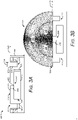
- Fig. 3A illustrates a cross-sectional side view of an example waveguide 102-2 with lobe suppression, in accordance with one or more implementations of the present disclosure.
- the waveguide 102-2 is an example of the waveguide 102 and 102-1.
- a cross-section of the pipe 104 is shown perpendicular to the longitudinal direction 128 and the latitudinal direction 126.
- the pipe 104 includes a surface 106 defining the parasitic groove 120 and the second parasitic groove 122, along with radiating slots 212 and 228.
- the pipe 104 may define an outer diameter 300 and an inner diameter 304.
- the dielectric 114 may fill the inner diameter 304.
- the inner diameter 304 may be defined by the channel 116.
- the parasitic groove 120 defines a depth 310.
- the depth 310 may be uniform or non-uniform across the entire parasitic groove 120.
- the depth 310 may include a portion that is less than the outer diameter 300. In another example, the depth 310 includes a portion that is less than the inner diameter 304.
- the parasitic groove 120 may be defined by a wall or walls 308 perpendicular to the surface at a vertex 306 of the walls 308 and the surface 106.
- the second parasitic groove 122 defines a depth 312.
- the depth 312 may be uniform or non-uniform across the entire second parasitic groove 122.
- the depth 312 may include a portion that is less than the outer diameter 300. In another example, the depth 312 includes a portion that is less than the inner diameter 304.
- Fig. 3B illustrates a side view of radiated grating lobes, in accordance with one or more implementations of the present disclosure.
- the pipe 104 defines the radiation pattern 254 according to the parasitic grooves 120 and 122 and the radiating slots 204, 208, 212, 216, 220, 224, and 228.
- the radiation pattern 254 includes the main lobe 256 and the grating lobes 258 and 260.
- the radiation energy of grating lobes 258 and 260 may be reduced by the parasitic grooves 120 and 122.
- Fig. 4 illustrates a top-down view of an example waveguide 102-3 with lobe suppression, in accordance with one or more implementations of the present disclosure.
- the waveguide 102-3 is an example of the waveguides 102, 102-1, and 102-2.
- the first radiating slots 204, 208, 212, and 216 are arranged in a first row 200, and the first row 200 may be parallel to the longitudinal direction 128.
- the first radiating slots 204, 208, 212, and 216 may define respective first centroids 206, 210, 214, and 218. In an example, centroids may be defined as a geometric center of the respective shape or radiating slot.
- Second radiating slots 220, 224, and 228 are arranged in a second row 202, and the second row 202 may be parallel to the longitudinal direction 128.
- the second radiating slots 220, 224, and 228 may define respective second centroids 222, 226, and 230.
- the radiating slots 204, 208, 212, 216, 220, 224, and 228 may be slots defined to radiate electromagnetic waves propagated through the pipe 104.
- the radiating slots 204, 208, 212, 216, 220, 224, and 228 may be various geometric shapes.
- the radiating slots 204, 208, 212, 216, 220, 224, and 228 may be defined within boundaries of the channel 246, communicating with the dielectric 114 or empty space defined therein.
- the first row 200 may be interleaved with the second row 202.
- the parasitic groove 120 may be defined on the surface 106.
- the parasitic groove 120 is defined in parallel with the longitudinal direction 128. As such, the parasitic groove 120 may be in parallel with the first row 200 and the second row 202 of radiating slots. The parasitic groove 120 may be spaced a first distance 242 from the first centroids 206, 210, 214, and 218 and spaced a second distance 244 from the second centroids 222, 226, and 230. The parasitic groove 120 may be spaced from the first centroids 206, 210, 214, and 218 and the second centroids 222, 226, and 230 in the latitudinal direction. In an example, the parasitic groove 120 defines a length 234.
- the length 234 may be defined as the longest measure between edges of the parasitic groove 120 and may be uniform or non-uniform across the parasitic groove 120. In the example, the length 234 is greater than a first-row length 410 (as shown in Fig. 4 ). The length 234 may also be greater than a second-row length 412 (also shown in Fig. 4 ).
- the parasitic groove 120 defines a width 236.
- the width 236 is defined in the latitudinal direction 126. In the example, the width 236 is related to a width of the radiating slots 204, 208, 212, 216, 220, 224, and 228, and the width 236 may be uniform or non-uniform across the parasitic groove 120.
- the pipe 104 of the waveguide 102-3 defines another parasitic groove 400.
- the other parasitic groove 400 may be similarly situated with regard to the parasitic groove 120, in parallel with the first row 200 and the second row 202.
- another width 404 similar to the width 236, and another length 402 similar to the length 234, may be defined by the other parasitic groove 400.
- the length 402 and other width 404 may be uniform or non-uniform across the other parasitic groove 400.
- the first centroids 206, 210, 214, and 218 may be spaced from the other parasitic groove 400 by a third distance 406, and the other parasitic groove 400 may be spaced a fourth distance 408 from the second centroids 222, 226, and 230.
- the other parasitic groove 400 can be spaced from the first centroids 206, 210, 214, and 218 and the second centroids 222, 226, and 230 in the latitudinal direction.
- the first distance 242 may be less than the third distance 406, and the second distance 244 may be less than the fourth distance 408.
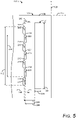
- Fig. 5 illustrates a top-down view of an example waveguide 102-4 with lobe suppression, in accordance with one or more implementations of the present disclosure.
- the waveguide 102-4 is an example of the waveguides 102, 102-1, 102-2, and 102-4.
- the first radiating slots 204, 208, 212, and 216 are arranged in a first row 200, and the first row 200 may be parallel to the longitudinal direction 128.
- the first radiating slots 204, 208, 212, and 216 may define respective first centroids 206, 210, 214, and 218.
- centroids may be defined as a geometric center of the respective shape or radiating slot.
- Second radiating slots 220, 224, and 228 are arranged in a second row 202, and the second row 202 may be parallel to the longitudinal direction 128.
- the second radiating slots 220, 224, and 228 may define respective second centroids 222, 226, and 230.
- the radiating slots 204, 208, 212, 216, 220, 224, and 228 may be radiating slots that radiate electromagnetic waves propagated through the pipe 104.
- the radiating slots 204, 208, 212, 216, 220, 224, and 228 may be various geometric shapes.
- the radiating slots 204, 208, 212, 216, 220, 224, and 228 may be defined within boundaries of the channel 246, communicating with the dielectric 114 or empty space defined therein.
- the first row 200 may be interleaved with the second row 202.
- the parasitic groove 120 may be defined on the surface 106.
- the parasitic groove 120 is defined in parallel with the longitudinal direction 128. As such, the parasitic groove 120 may be in parallel with the first row 200 and the second row 202. The parasitic groove 120 may be spaced a first distance 242 from the first centroids 206, 210, 214, and 218 and spaced a second distance 244 from the second centroids 222, 226, and 230. The parasitic groove 120 may be spaced from the first centroids 206, 210, 214, and 218 and the second centroids 222, 226, and 230 in the latitudinal direction. In an example, the parasitic groove 120 defines a groove length 234.
- the groove length 234 may be defined as the longest measure between edges of the parasitic groove 120 and may be uniform or non-uniform across the groove 120. In the example, the length 234 is greater than a first-row length 410 (as shown in Fig. 4 ). The length 234 may also be greater than a second-row length 412 (also shown in Fig. 4 ).
- the parasitic groove 120 defines a width 236.
- the width 236 is defined in the latitudinal direction 126. In the example, the width 236 is related to a width of the radiating slots 204, 208, 212, 216, 220, 224, and 228, and the width 236 may be uniform or non-uniform across the parasitic groove 120.
- an example method 600 in accordance with one or more implementations of the present disclosure.
- the method 600 is shown as a set of blocks that specify operations and steps performed but are not necessarily limited to the order or combinations shown for performing the operations by the respective blocks. Further, any of one or more of the operations may be repeated, combined, reorganized, omitted, or linked to provide a wide array of additional and/or alternate methods.
- electromagnetic waves are propagated through the waveguide 102.
- the transceiver 110 may output electromagnetic waves through the coupler 108 into the channel 246.
- electromagnetic waves are propagated through the channel 246 and out of the radiating slots 118.
- the electromagnetic waves are suppressed by the groove 120, groove 122, groove 400, other grooves not specifically depicted, or any combination thereof.
- first, second, and other are only used to provide clarity and designation of elements.
- first row 200 and the second row 202 may be interchanged and are only used for clarity when referring to the instant figures.
- "at least one of: a, b, or c” is intended to cover a, b, c, a-b, a-c, b-c, and a-b-c, as well as any combination with multiples of the same element (e.g., a-a, a-a-a, a-a-b, a-a-c, a-b-b, a-c-c, b-b, b-b-b, b-b-c, c-c, and c-c-c or any other ordering of a, b, and c).
Landscapes
- Engineering & Computer Science (AREA)
- Radar, Positioning & Navigation (AREA)
- Remote Sensing (AREA)
- Physics & Mathematics (AREA)
- Computer Networks & Wireless Communication (AREA)
- General Physics & Mathematics (AREA)
- Computer Security & Cryptography (AREA)
- Mechanical Engineering (AREA)
- Electromagnetism (AREA)
- Waveguide Aerials (AREA)
- Variable-Direction Aerials And Aerial Arrays (AREA)
Abstract
Description
- Some devices (e.g., radar) use electromagnetic signals to detect and track objects. The electromagnetic signals are transmitted and received using one or more antennas. An antenna may be characterized in terms of gain, beam width, or, more specifically, pattern, which is a measure of the gain as a function of direction. A precisely controlled pattern may improve applications that require electromagnetic signals, and a waveguide may be used to improve such characteristics. The waveguide can include perforations or radiating slots that guide radiation near the antenna. Grating lobes, or secondary main lobes, may arise when the perforation spacing is greater than one-half wavelength of the transceiver signal.
- This document describes techniques, apparatuses, and systems for a waveguide with lobe suppression. In some examples, an apparatus may include a waveguide including a pipe for containing a dielectric, the pipe defining an open end to a longitudinal direction through the pipe, and further including an array of radiating slots through a surface of the pipe and in communication with the dielectric. The waveguide further including at least one parasitic groove separate from the pipe and with at least a portion of a length that is parallel to the array of radiating slots.
- In some examples, a system may include a coupler, a transceiver operable upon actuation to interact with electromagnetic waves associated with the coupler, and a waveguide. The waveguide includes a pipe for capturing the electromagnetic waves and containing a dielectric, the pipe defining an open end to a longitudinal direction through the pipe. The waveguide further including an array of radiating slots through a surface of the pipe and in communication with the dielectric, and at least one parasitic groove separate from the pipe and with at least a portion of a length that is parallel to the array of radiating slots.
- In this way, the waveguide provides an antenna pattern where grating lobes are suppressed or substantially reduced. This document also describes other configurations and systems for providing lobe suppression.
- This Summary introduces simplified concepts related to lobe suppression for waveguides with lobe suppression, which are further described below in the Detailed Description and Drawings. This Summary is not intended to identify essential features of the claimed subject matter, nor is it intended for use in determining the scope of the claimed subject matter.
- The details of one or more aspects of waveguides with lobe suppression are described in this document with reference to the following drawings. The same numbers are used throughout the drawings to reference like features and components:
-
Fig. 1 illustrates an example system with an example waveguide with lobe suppression, in accordance with one or more implementations of the present disclosure; -
Fig. 2A illustrates a top-down view of an example waveguide with lobe suppression, in accordance with one or more implementations of the present disclosure; -
Fig. 2B illustrates a plan view and radiating pattern of the example waveguide shown in 2A; -
Fig. 3A illustrates a cross-sectional side view of an example waveguide with lobe suppression, in accordance with one or more implementations of the present disclosure; -
Fig. 3B illustrates a side view of radiated grating lobes, in accordance with one or more implementations of the present disclosure; -
Fig. 4 illustrates a top-down view of an example waveguide with lobe suppression, in accordance with one or more implementations of the present disclosure; -
Fig. 5 illustrates a top-down view of an example waveguide with lobe suppression, in accordance with one or more implementations of the present disclosure; and -
Fig. 6 illustrates an example method performed with a waveguide with lobe suppression, in accordance with one or more implementations of the present disclosure. - Radar systems are a sensing technology used in many industries (including the automotive industry) to acquire information about the surrounding environment. An antenna, such as one described herein, may be employed in radar systems to transmit and receive electromagnetic energy or signals. Such a radar system may use multiple antenna-elements in an array to provide increased gain and directivity over what can be achieved using a single antenna-element. As taught herein, signals from the individual elements are combined with appropriate phases and weighted amplitudes to provide the desired antenna-reception pattern during reception. The antenna arrays are also used in transmission, splitting signal power amongst the elements and using appropriate phases and weighted amplitudes to provide the desired antenna transmission pattern.
- Consider, for example, a waveguide employed to transfer electromagnetic energy to and from the antenna elements. The waveguide can include an array of radiating slots. The radiating slots represent apertures of the waveguide, which may be arranged to provide desired phasing, combining, or splitting of signals and energy. As an example, the radiating slots, which may also sometimes referred to as apertures, may be equally spaced in a surface of the waveguide, along a propagation direction of the electromagnetic waves. The radiating slots may cause grating lobes to appear in an antenna pattern. The size and shape of the grating lobes are based on the spacing and arrangement of the array of radiating slots. Reduced form factors may cause undesired grating lobe propagation according to ratios between radiating slot lengths, radiating slot spacing, wavelengths of the electromagnetic signal, and other organizational factors associated with the waveguide. The geometry of the waveguide may be adjusted, or the radiating slots may be rearranged in an attempt to reduce grating lobes below design specifications.
- In contrast to this and other techniques, a waveguide with lobe suppression is described. To suppress grating lobes in an antenna pattern, the waveguide includes at least one parasitic groove that is separate from the pipe and with at least a portion of a length that is parallel to the array of radiating slots. The at least one parasitic groove has a uniform narrow width and uniform depth and is spaced apart from an array of radiating slots to achieve the desired lobe suppression. The parasitic groove is in a same surface of the waveguide, which defines the array of radiating slots. This parasitic groove may be defined according to various geometric shapes. As one example, the grooves may be linear and arranged in parallel to the radiating slots. In this way, the waveguide provides an antenna pattern where grating lobes are suppressed or substantially reduced.
- The example waveguide may be particularly advantageous for use in an automotive context, for example, detecting objects in a roadway. The grating lobes can indicate false detections within an automotive radar field-of-view. Suppressing these grating lobes improves accuracy of the radar as the number of false detections is reduced.
- In this way, the present disclosure describes lobe suppression with a waveguide. Indeed, such application of this and other examples provided in this disclosure increased radiation performance of a waveguide. These are but a few examples of how the described techniques and devices may be used to suppress grating lobes for multi-element waveguides. The document now turns to an example operating environment, after which example devices, methods, and systems are described.
-
Fig. 1 illustrates anexample system 100 that includes awaveguide 102 in accordance with techniques, apparatuses, and systems of this disclosure. Thesystem 100 includes thewaveguide 102, acoupler 108, atransceiver 110. Thetransceiver 110 may be operable upon actuation to interact with electromagnetic waves associated with thecoupler 108 and thewaveguide 102. - The
transceiver 110 may be a variety of components and may be a receiver or transmitter only. Thecoupler 108 is a link between thetransceiver 110 and thewaveguide 102 and may be a coaxial cable or another implement that connects through theopen end 112 of thewaveguide 102, forming an antenna assembly. Theopen end 112 may be opposite a closed end of thepipe 104. Theopen end 112 may define an opening such that the open end borders the dielectric 114 and defines an opening to achannel 116 through thepipe 104. - The
waveguide 102 includes apipe 104. Thepipe 104 may comprise various materials having various geometric shapes. Thepipe 104 may be formed from metal to have a rectangular cross-section. Other non-exhaustive examples include cylindrical or square cross-sections. - The
pipe 104 includes an array of radiatingslots 118 arranged on asurface 106 of thewaveguide 102. The radiatingslots 118 may be in communication with the dielectric 114, allowing electromagnetic waves propagated through the dielectric to bidirectionally flow through the radiatingslots 118. The dielectric 114 may be any material. As an example, the dielectric 114 may be air from an environment surrounding thewaveguide 102. Dielectric contained within thepipe 104 of thewaveguide 102 may be reduced or removed to generate a vacuum volume defined by thewaveguide 102. - Separate from the
pipe 104, thewaveguide 102 includes aparasitic groove 120. Theparasitic groove 120 may be implemented as various geometric shapes. In one example, theparasitic groove 120 may be linear and defined in parallel to the radiatingslots 118. A secondparasitic groove 122 of thewaveguide 102 may be separate from thepipe 104. The secondparasitic groove 122 may be similar to theparasitic groove 120 but on an opposite side of the radiatingslots 118. Theparasitic grooves pipe 104 and may be on a same side of the radiatingslots 118 to achieve a particular suppression of grating lobes. - The
pipe 104 defines alongitudinal direction 128 and alatitudinal direction 126 perpendicular to thelongitudinal direction 128. Theparasitic grooves longitudinal direction 128. A propagation direction defined in the direction of electromagnetic waves traversing thepipe 104 and emanating from thecoupler 108 may also be in parallel with thelongitudinal direction 128. In this way, theparasitic grooves pipe 104. -
Fig. 2A illustrates a top-down view of an example waveguide 102-1 with lobe suppression, in accordance with one or more implementations of the present disclosure. The waveguide 102-1 shown inFig. 2A illustrates similar components to those depicted inFig. 1 and is therefore an example of the waveguide 102-1. Thepipe 104 defines asurface 106. Radiatingslots 118 may be defined by thepipe 104 through thesurface 106. First radiatingslots first row 200, and thefirst row 200 may be parallel to thelongitudinal direction 128. Thefirst radiating slots first centroids slots 220, 224, and 228 are arranged in asecond row 202, and thesecond row 202 may be parallel to thelongitudinal direction 128. Thesecond radiating slots 220, 224, and 228 may define respectivesecond centroids 222, 226, and 230. The radiatingslots pipe 104. The radiatingslots slots Fig. 2A ), communicating with the dielectric 114 or empty space defined therein. - The
first row 200 may be interleaved with thesecond row 202. As an example, thefirst row 200 overlaps with thesecond row 202 in thelongitudinal direction 128. Thefirst radiating slots second radiating slots 220, 224, and 228 in thelongitudinal direction 128 forming a row or pseudo row (e.g., radiatingslots first radiating slots second radiating slots 220, 224, and 228 in thelatitudinal direction 126 according to therespective centroids first centroids longitudinal direction 128, and thesecond centroids 222, 226, and 230 may be aligned in thelongitudinal direction 128. - In an example,
parasitic groove 120 is defined on thesurface 106, and theparasitic groove 120 is defined in parallel with thelongitudinal direction 128. As such, theparasitic groove 120 may be in parallel with thefirst row 200 and thesecond row 202. - The
parasitic groove 120 may be spaced afirst distance 242 from thefirst centroids second distance 244 from thesecond centroids 222, 226, and 230. Theparasitic groove 120 may be spaced from thefirst centroids second centroids 222, 226, and 230 in the latitudinal direction. In an example, theparasitic groove 120 defines alength 234. Thelength 234 may be defined as the longest measure between edges of theparasitic groove 120 and may be uniform or non-uniform across thegroove 120. In the example, thelength 234 is greater than a first-row length 410 (as shown inFig. 4 ). The first-row length 410 may be a collective length of all of the radiatingslots row length 410 added to the second-row length 412. Thelength 234 may also be greater than a second-row length 412 (also shown inFig. 4 ). - In the example, the
parasitic groove 120 defines awidth 236. Thewidth 236 is defined in thelatitudinal direction 126 and may be less than aradiating slot width 232. The radiatingslot width 232 may be uniform or non-uniform for all of the radiatingslots slots width 236 is related to a width of the radiatingslots width 236 may be uniform or non-uniform across theparasitic groove 120. - A second
parasitic groove 122 may be defined on thesurface 106. The secondparasitic groove 122 and theparasitic groove 120 may bound one or more of the radiatingslots parasitic groove 120 and the secondparasitic groove 122 may bound the radiatingslots parasitic groove 122 defines alength 238 and awidth 240. Thelength 238 and thewidth 240 may be uniform or non-uniform across respective portions of the secondparasitic groove 122. Thelength 238 may be equal to thelength 234, and thewidth 240 may be equal to thewidth 236. As such, the secondparasitic groove 122 may be in parallel with thefirst row 200 and thesecond row 202. The secondparasitic groove 122 may be spaced thefirst distance 242 from thesecond centroids 222, 226, and 230 and spaced thesecond distance 244 fromfirst centroids parasitic groove 120 may be spaced from thefirst centroids second centroids 222, 226, and 230 in the latitudinal direction. -
Fig. 2B illustrates a plan view andradiating pattern 254 of the example waveguide shown in 2A. When propagating, thepipe 104 radiates electromagnetic waves similar toradiation pattern 254 with respect to the definedlongitudinal direction 128 andlatitudinal direction 126. - The
radiation pattern 254 includes amain lobe 256 and associated gratinglobes grooves Fig. 2A may be defined to reduce thegrating lobes parasitic grooves grating lobes -
Fig. 3A illustrates a cross-sectional side view of an example waveguide 102-2 with lobe suppression, in accordance with one or more implementations of the present disclosure. The waveguide 102-2 is an example of thewaveguide 102 and 102-1. - A cross-section of the
pipe 104 is shown perpendicular to thelongitudinal direction 128 and thelatitudinal direction 126. Thepipe 104 includes asurface 106 defining theparasitic groove 120 and the secondparasitic groove 122, along with radiatingslots pipe 104 may define anouter diameter 300 and aninner diameter 304. The dielectric 114 may fill theinner diameter 304. Theinner diameter 304 may be defined by thechannel 116. - The
parasitic groove 120 defines adepth 310. Thedepth 310 may be uniform or non-uniform across the entireparasitic groove 120. Thedepth 310 may include a portion that is less than theouter diameter 300. In another example, thedepth 310 includes a portion that is less than theinner diameter 304. Theparasitic groove 120 may be defined by a wall orwalls 308 perpendicular to the surface at avertex 306 of thewalls 308 and thesurface 106. - The second
parasitic groove 122 defines adepth 312. Thedepth 312 may be uniform or non-uniform across the entire secondparasitic groove 122. Thedepth 312 may include a portion that is less than theouter diameter 300. In another example, thedepth 312 includes a portion that is less than theinner diameter 304. -
Fig. 3B illustrates a side view of radiated grating lobes, in accordance with one or more implementations of the present disclosure. Thepipe 104 defines theradiation pattern 254 according to theparasitic grooves slots radiation pattern 254 includes themain lobe 256 and thegrating lobes lobes parasitic grooves -
Fig. 4 illustrates a top-down view of an example waveguide 102-3 with lobe suppression, in accordance with one or more implementations of the present disclosure. The waveguide 102-3 is an example of thewaveguides 102, 102-1, and 102-2. - In the waveguide 102-3, the
first radiating slots first row 200, and thefirst row 200 may be parallel to thelongitudinal direction 128. Thefirst radiating slots first centroids slots 220, 224, and 228 are arranged in asecond row 202, and thesecond row 202 may be parallel to thelongitudinal direction 128. Thesecond radiating slots 220, 224, and 228 may define respectivesecond centroids 222, 226, and 230. The radiatingslots pipe 104. The radiatingslots slots channel 246, communicating with the dielectric 114 or empty space defined therein. Thefirst row 200 may be interleaved with thesecond row 202. Theparasitic groove 120 may be defined on thesurface 106. - In an example, the
parasitic groove 120 is defined in parallel with thelongitudinal direction 128. As such, theparasitic groove 120 may be in parallel with thefirst row 200 and thesecond row 202 of radiating slots. Theparasitic groove 120 may be spaced afirst distance 242 from thefirst centroids second distance 244 from thesecond centroids 222, 226, and 230. Theparasitic groove 120 may be spaced from thefirst centroids second centroids 222, 226, and 230 in the latitudinal direction. In an example, theparasitic groove 120 defines alength 234. Thelength 234 may be defined as the longest measure between edges of theparasitic groove 120 and may be uniform or non-uniform across theparasitic groove 120. In the example, thelength 234 is greater than a first-row length 410 (as shown inFig. 4 ). Thelength 234 may also be greater than a second-row length 412 (also shown inFig. 4 ). In the example, theparasitic groove 120 defines awidth 236. Thewidth 236 is defined in thelatitudinal direction 126. In the example, thewidth 236 is related to a width of the radiatingslots width 236 may be uniform or non-uniform across theparasitic groove 120. - The
pipe 104 of the waveguide 102-3 defines anotherparasitic groove 400. The otherparasitic groove 400 may be similarly situated with regard to theparasitic groove 120, in parallel with thefirst row 200 and thesecond row 202. anotherwidth 404 similar to thewidth 236, and anotherlength 402 similar to thelength 234, may be defined by the otherparasitic groove 400. Thelength 402 andother width 404 may be uniform or non-uniform across the otherparasitic groove 400. Thefirst centroids parasitic groove 400 by athird distance 406, and the otherparasitic groove 400 may be spaced afourth distance 408 from thesecond centroids 222, 226, and 230. The otherparasitic groove 400 can be spaced from thefirst centroids second centroids 222, 226, and 230 in the latitudinal direction. Thefirst distance 242 may be less than thethird distance 406, and thesecond distance 244 may be less than thefourth distance 408. -
Fig. 5 illustrates a top-down view of an example waveguide 102-4 with lobe suppression, in accordance with one or more implementations of the present disclosure. The waveguide 102-4 is an example of thewaveguides 102, 102-1, 102-2, and 102-4. - In the example, the
first radiating slots first row 200, and thefirst row 200 may be parallel to thelongitudinal direction 128. Thefirst radiating slots first centroids slots 220, 224, and 228 are arranged in asecond row 202, and thesecond row 202 may be parallel to thelongitudinal direction 128. Thesecond radiating slots 220, 224, and 228 may define respectivesecond centroids 222, 226, and 230. The radiatingslots pipe 104. The radiatingslots slots channel 246, communicating with the dielectric 114 or empty space defined therein. Thefirst row 200 may be interleaved with thesecond row 202. Theparasitic groove 120 may be defined on thesurface 106. - In an example, the
parasitic groove 120 is defined in parallel with thelongitudinal direction 128. As such, theparasitic groove 120 may be in parallel with thefirst row 200 and thesecond row 202. Theparasitic groove 120 may be spaced afirst distance 242 from thefirst centroids second distance 244 from thesecond centroids 222, 226, and 230. Theparasitic groove 120 may be spaced from thefirst centroids second centroids 222, 226, and 230 in the latitudinal direction. In an example, theparasitic groove 120 defines agroove length 234. Thegroove length 234 may be defined as the longest measure between edges of theparasitic groove 120 and may be uniform or non-uniform across thegroove 120. In the example, thelength 234 is greater than a first-row length 410 (as shown inFig. 4 ). Thelength 234 may also be greater than a second-row length 412 (also shown inFig. 4 ). In the example, theparasitic groove 120 defines awidth 236. Thewidth 236 is defined in thelatitudinal direction 126. In the example, thewidth 236 is related to a width of the radiatingslots width 236 may be uniform or non-uniform across theparasitic groove 120. - Referring to
Fig. 6 , anexample method 600 in accordance with one or more implementations of the present disclosure. Themethod 600 is shown as a set of blocks that specify operations and steps performed but are not necessarily limited to the order or combinations shown for performing the operations by the respective blocks. Further, any of one or more of the operations may be repeated, combined, reorganized, omitted, or linked to provide a wide array of additional and/or alternate methods. In portions of the following discussion, reference may be made to the examples of the preceding figures, reference to which is made for example only. The techniques are not limited to performance by one entity or multiple entities operating on one device. - At 602, electromagnetic waves are propagated through the
waveguide 102. As an example, thetransceiver 110 may output electromagnetic waves through thecoupler 108 into thechannel 246. - At 604, electromagnetic waves are propagated through the
channel 246 and out of the radiatingslots 118. At 606, the electromagnetic waves are suppressed by thegroove 120,groove 122,groove 400, other grooves not specifically depicted, or any combination thereof. - As referenced herein, adjectives, including first, second, and other, are only used to provide clarity and designation of elements. As an example, the
first row 200 and thesecond row 202 may be interchanged and are only used for clarity when referring to the instant figures. - The following are some additional examples of a waveguide with lobe suppression:
- Example 1. An apparatus, the apparatus comprising: a waveguide including: a pipe for containing a dielectric, the pipe defining an open end to a longitudinal direction through the pipe; an array of radiating slots through a surface of the pipe and in communication with the dielectric; and at least one parasitic groove separate from the pipe and with a length that is in parallel with the array of radiating slots.
- Example 2. The waveguide of any preceding example, wherein the at least one parasitic groove is spaced a first distance from the array of radiating slots to suppress grating lobes in an antenna pattern.
- Example 3. The waveguide of any preceding example, wherein the at least one parasitic groove has a depth less than a depth of the pipe.
- Example 4. The waveguide of any preceding example, wherein the at least one parasitic groove has a depth that is uniform.
- Example 5. The waveguide of any preceding example, wherein the at least one parasitic groove has a narrow width that is uniform.
- Example 6. The waveguide of any preceding example, wherein the pipe has a closed end opposite the open end.
- Example 7. The waveguide of any preceding example, wherein the at least one parasitic groove has a length that extends along an entire length of the array of radiating slots.
- Example 8. The waveguide of any preceding example, wherein the at least one parasitic groove has a length that extends beyond a length of the array of radiating slots.
- Example 9. The waveguide of any preceding example, further comprising, a second parasitic groove separate from the pipe and in parallel with the first parasitic groove and the array of radiating slots.
- Example 10. The waveguide of any preceding example, wherein the second parasitic groove is on a first side of the array of radiating slots and the at least one parasitic groove is on an opposite side of the array of radiating slots.
- Example 11. The waveguide of any preceding example, wherein the longitudinal direction is parallel to a propagation direction associated with the waveguide.
- Example 12. A system, the system comprising: a coupler; a transceiver operable upon actuation to interact with electromagnetic waves associated with the coupler; and a waveguide comprising: a pipe for capturing the electromagnetic waves and containing a dielectric, the pipe defining an open end to a longitudinal direction through the pipe; an array of radiating slots through a surface of the pipe and in communication with the dielectric; and at least one parasitic groove separate from the pipe and with a length that is in parallel with the array of radiating slots.
- Example 13. The system of any preceding example, wherein the at least one parasitic groove is spaced a first distance from the array of radiating slots to suppress grating lobes in an antenna pattern.
- Example 14. The system of any preceding example, wherein the at least one parasitic groove has a depth less than a depth of the pipe.
- Example 15. The system of any preceding example, wherein the at least one parasitic groove has a depth that is uniform.
- Example 16. The system of any preceding example, wherein the at least one parasitic groove has a narrow width that is uniform.
- Example 17. The system of any preceding example, wherein the pipe has a closed end opposite the open end.
- Example 18. The system of any preceding example, wherein the at least one parasitic groove has a length that extends along an entire length of the array of radiating slots.
- Example 19. The system of any preceding example, wherein the system comprises part of an automobile that detects the electromagnetic waves for operating on a roadway.
- Example 20. The system of any preceding example, wherein the at least one parasitic groove comprises a first parasitic groove on a first side of the array of radiating slots and a second parasitic groove on a second, opposite side of the array of radiating slots.
- While various embodiments of the disclosure are described in the foregoing description and shown in the drawings, it is to be understood that this disclosure is not limited thereto but may be variously embodied to practice within the scope of the following claims. From the foregoing description, it will be apparent that various changes may be made without departing from the spirit and scope of the disclosure as defined by the following claims.
- The use of "or" and grammatically related terms indicates non-exclusive alternatives without limitation unless the context clearly dictates otherwise. As used herein, a phrase referring to "at least one of' a list of items refers to any combination of those items, including single members. As an example, "at least one of: a, b, or c" is intended to cover a, b, c, a-b, a-c, b-c, and a-b-c, as well as any combination with multiples of the same element (e.g., a-a, a-a-a, a-a-b, a-a-c, a-b-b, a-c-c, b-b, b-b-b, b-b-c, c-c, and c-c-c or any other ordering of a, b, and c).
Claims (15)
- An apparatus, the apparatus comprising:
a waveguide including:a pipe for containing a dielectric, the pipe defining an open end to a longitudinal direction through the pipe;an array of radiating slots through a surface of the pipe and in communication with the dielectric; andat least one parasitic groove separate from the pipe and with at least a portion of a length that is parallel to the array of radiating slots. - The waveguide of claim 1,
wherein the at least one parasitic groove is spaced a first distance from the array of radiating slots to suppress grating lobes in an antenna pattern. - The waveguide of any of the preceding claims,
wherein the at least one parasitic groove has a depth less than a depth of the pipe. - The waveguide of any of the preceding claims,
wherein the at least one parasitic groove has a depth that is uniform. - The waveguide of any of the preceding claims,
wherein the at least one parasitic groove has a uniform width. - The waveguide of any of the preceding claims,
wherein the pipe has a closed end opposite the open end. - The waveguide of any of the preceding claims,
wherein the at least one parasitic groove has a length that extends along an entire length of the array of radiating slots. - The waveguide of claim 7,
wherein the at least one parasitic groove has a length that extends beyond a length of the array of radiating slots. - The waveguide of any of the preceding claims, further comprising:
another parasitic groove that is separate from the pipe and parallel to the parasitic groove and the array of radiating slots. - The waveguide of claim 9,
wherein the other parasitic groove is on a first side of the array of radiating slots and the parasitic groove is on an opposite side of the array of radiating slots. - The waveguide of any of the preceding claims,
wherein the longitudinal direction is parallel to a propagation direction associated with the waveguide. - The waveguide of any of the preceding claims,
wherein the waveguide comprises part of an automobile that detects electromagnetic waves for operating on a roadway. - The waveguide of claim 12,
wherein the part of the automobile comprises a radar system for detecting the electromagnetic waves for operating the automobile on the roadway. - A system comprising:the waveguide of any of claims 1-13; anda radar system for transceiving the electromagnetic waves detected using the waveguide of any of claims 1-13.
- The system of claim 14, wherein the radar system comprises part of an automobile for operating on a roadway based on the electromagnetic waves.
Applications Claiming Priority (1)
| Application Number | Priority Date | Filing Date | Title |
|---|---|---|---|
| US17/162,664 US11668787B2 (en) | 2021-01-29 | 2021-01-29 | Waveguide with lobe suppression |
Publications (3)
| Publication Number | Publication Date |
|---|---|
| EP4037097A1 true EP4037097A1 (en) | 2022-08-03 |
| EP4037097B1 EP4037097B1 (en) | 2024-04-10 |
| EP4037097B8 EP4037097B8 (en) | 2024-05-22 |
Family
ID=78822313
Family Applications (1)
| Application Number | Title | Priority Date | Filing Date |
|---|---|---|---|
| EP21212703.9A Active EP4037097B8 (en) | 2021-01-29 | 2021-12-07 | Waveguide with lobe suppression |
Country Status (3)
| Country | Link |
|---|---|
| US (1) | US11668787B2 (en) |
| EP (1) | EP4037097B8 (en) |
| CN (1) | CN114824747A (en) |
Cited By (1)
| Publication number | Priority date | Publication date | Assignee | Title |
|---|---|---|---|---|
| WO2025115994A1 (en) * | 2023-11-29 | 2025-06-05 | ソニーグループ株式会社 | Waveguide structure and antenna device |
Families Citing this family (5)
| Publication number | Priority date | Publication date | Assignee | Title |
|---|---|---|---|---|
| US12015201B2 (en) * | 2021-11-05 | 2024-06-18 | Magna Electronics, Llc | Waveguides and waveguide sensors with signal-improving grooves and/or slots |
| DE102023124524A1 (en) | 2023-09-12 | 2025-03-13 | Valeo Schalter Und Sensoren Gmbh | Waveguide antenna device for a radar system, transmitter-receiver device, radar system, driver assistance system, vehicle and method for operating a waveguide antenna device |
| CN117855812B (en) * | 2024-01-29 | 2024-07-26 | 中国科学院上海微系统与信息技术研究所 | A waveguide antenna array and communication module |
| DE102024202153A1 (en) * | 2024-03-07 | 2025-09-11 | Robert Bosch Gesellschaft mit beschränkter Haftung | Antenna device and method for producing an antenna device |
| TWI910972B (en) * | 2024-12-18 | 2026-01-01 | 智易科技股份有限公司 | Radar antenna device and radar element thereof |
Citations (1)
| Publication number | Priority date | Publication date | Assignee | Title |
|---|---|---|---|---|
| US20200287293A1 (en) * | 2019-03-06 | 2020-09-10 | Aptiv Technologies Limited | Slot array antenna including parasitic features |
Family Cites Families (121)
| Publication number | Priority date | Publication date | Assignee | Title |
|---|---|---|---|---|
| US3032762A (en) * | 1959-01-02 | 1962-05-01 | John L Kerr | Circularly arrayed slot antenna |
| US3328800A (en) | 1964-03-12 | 1967-06-27 | North American Aviation Inc | Slot antenna utilizing variable standing wave pattern for controlling slot excitation |
| US3462713A (en) | 1967-07-19 | 1969-08-19 | Bell Telephone Labor Inc | Waveguide-stripline transducer |
| US3594806A (en) | 1969-04-02 | 1971-07-20 | Hughes Aircraft Co | Dipole augmented slot radiating elements |
| US3579149A (en) | 1969-12-08 | 1971-05-18 | Westinghouse Electric Corp | Waveguide to stripline transition means |
| NL7609903A (en) | 1976-09-07 | 1978-03-09 | Philips Nv | MICROWAVE DEVICE FOR CONVERTING A WAVE PIPE INTO A MICROSTRIP GUIDE STRUCTURE. |
| US4453142A (en) | 1981-11-02 | 1984-06-05 | Motorola Inc. | Microstrip to waveguide transition |
| US4562416A (en) | 1984-05-31 | 1985-12-31 | Sanders Associates, Inc. | Transition from stripline to waveguide |
| US4590480A (en) | 1984-08-31 | 1986-05-20 | Rca Corporation | Broadcast antenna which radiates horizontal polarization towards distant locations and circular polarization towards nearby locations |
| GB2463711B (en) | 1987-03-31 | 2010-09-29 | Dassault Electronique | Double polarization flat array antenna |
| US5030965A (en) | 1989-11-15 | 1991-07-09 | Hughes Aircraft Company | Slot antenna having controllable polarization |
| IL107582A (en) | 1993-11-12 | 1998-02-08 | Ramot Ramatsity Authority For | Slotted waveguide array antennas |
| US5986527A (en) | 1995-03-28 | 1999-11-16 | Murata Manufacturing Co., Ltd. | Planar dielectric line and integrated circuit using the same line |
| JP3366552B2 (en) | 1997-04-22 | 2003-01-14 | 京セラ株式会社 | Dielectric waveguide line and multilayer wiring board including the same |
| WO1999034477A1 (en) | 1997-12-29 | 1999-07-08 | Hsin Hsien Chung | Low cost high performance portable phased array antenna system for satellite communication |
| CA2292064C (en) | 1998-12-25 | 2003-08-19 | Murata Manufacturing Co., Ltd. | Line transition device between dielectric waveguide and waveguide, and oscillator and transmitter using the same |
| US6166701A (en) | 1999-08-05 | 2000-12-26 | Raytheon Company | Dual polarization antenna array with radiating slots and notch dipole elements sharing a common aperture |
| US6590477B1 (en) | 1999-10-29 | 2003-07-08 | Fci Americas Technology, Inc. | Waveguides and backplane systems with at least one mode suppression gap |
| AU2000277887A1 (en) | 2000-10-18 | 2002-04-29 | Nokia Corporation | Waveguide to stripline transition |
| EP1346431A1 (en) | 2000-12-21 | 2003-09-24 | Paratek Microwave, Inc. | Waveguide to microstrip transition |
| US6967347B2 (en) | 2001-05-21 | 2005-11-22 | The Regents Of The University Of Colorado | Terahertz interconnect system and applications |
| US6956537B2 (en) * | 2001-09-12 | 2005-10-18 | Kathrein-Werke Kg | Co-located antenna array for passive beam forming |
| WO2003044896A1 (en) * | 2001-11-20 | 2003-05-30 | Anritsu Corporation | Waveguide slot type radiator having construction to facilitate manufacture |
| JP2003289201A (en) | 2002-03-28 | 2003-10-10 | Anritsu Corp | Post-wall waveguide and junction conversion structure for cavity waveguide |
| US20070054064A1 (en) | 2003-12-26 | 2007-03-08 | Tadahiro Ohmi | Microwave plasma processing method, microwave plasma processing apparatus, and its plasma head |
| US7091919B2 (en) | 2003-12-30 | 2006-08-15 | Spx Corporation | Apparatus and method to increase apparent resonant slot length in a slotted coaxial antenna |
| US7034774B2 (en) | 2004-04-22 | 2006-04-25 | Northrop Grumman Corporation | Feed structure and antenna structures incorporating such feed structures |
| US7098070B2 (en) | 2004-11-16 | 2006-08-29 | International Business Machines Corporation | Device and method for fabricating double-sided SOI wafer scale package with through via connections |
| CN2796131Y (en) | 2005-05-30 | 2006-07-12 | 东南大学 | Multilayer substrate integrated wave guide elliptical response filter |
| FR2886773B1 (en) | 2005-06-03 | 2007-09-07 | Thales Sa | DISPERSIVE ANTENNA IN FREQUENCY APPLIED IN PARTICULAR TO WEATHER RADAR |
| WO2007114391A1 (en) | 2006-03-31 | 2007-10-11 | Kyocera Corporation | Dielectric waveguide device; phase shifter, high frequency switch, and attenuator provided with dielectric waveguide device; and method of manufacturing high frequency transmitter, high frequency receiver, high frequency transmitter/receiver and radar device, array antenna, and dielectric waveguide device |
| CN101915957B (en) | 2006-06-12 | 2012-12-12 | 加利福尼亚太平洋生物科学公司 | Substrates for performing analytical reactions |
| KR100846872B1 (en) | 2006-11-17 | 2008-07-16 | 한국전자통신연구원 | Apparatus for the transition of dielectric waveguide and transmission line in millimeter wave band |
| JP4365852B2 (en) | 2006-11-30 | 2009-11-18 | 株式会社日立製作所 | Waveguide structure |
| EP1936741A1 (en) | 2006-12-22 | 2008-06-25 | Sony Deutschland GmbH | Flexible substrate integrated waveguides |
| US8231284B2 (en) | 2007-03-26 | 2012-07-31 | International Business Machines Corporation | Ultra-high bandwidth, multiple-channel full-duplex, single-chip CMOS optical transceiver |
| US7768457B2 (en) | 2007-06-22 | 2010-08-03 | Vubiq, Inc. | Integrated antenna and chip package and method of manufacturing thereof |
| US8159316B2 (en) | 2007-12-28 | 2012-04-17 | Kyocera Corporation | High-frequency transmission line connection structure, circuit board, high-frequency module, and radar device |
| WO2009107216A1 (en) | 2008-02-28 | 2009-09-03 | 三菱電機株式会社 | Waveguide slot array antenna apparatus |
| CA2629035A1 (en) | 2008-03-27 | 2009-09-27 | Her Majesty The Queen In Right Of Canada, As Represented By The Minister Of Industry, Through The Communications Research Centre Canada | Waveguide filter with broad stopband based on sugstrate integrated waveguide scheme |
| JP5172481B2 (en) | 2008-06-05 | 2013-03-27 | 株式会社東芝 | Short slot directional coupler with post-wall waveguide, butler matrix and on-vehicle radar antenna using the same |
| US8089327B2 (en) | 2009-03-09 | 2012-01-03 | Toyota Motor Engineering & Manufacturing North America, Inc. | Waveguide to plural microstrip transition |
| KR101327375B1 (en) | 2009-03-31 | 2013-11-08 | 쿄세라 코포레이션 | Waveguide structure, high frequency module including waveguide structure, and radar apparatus |
| CN201383535Y (en) | 2009-04-01 | 2010-01-13 | 惠州市硕贝德通讯科技有限公司 | Rectangular waveguide-substrate integrated waveguide signal conversion and power divider |
| WO2010127709A1 (en) | 2009-05-08 | 2010-11-11 | Telefonaktiebolaget L M Ericsson (Publ) | A transition from a chip to a waveguide port |
| US8604990B1 (en) | 2009-05-23 | 2013-12-10 | Victory Microwave Corporation | Ridged waveguide slot array |
| CN101645539A (en) * | 2009-08-28 | 2010-02-10 | 中国科学院光电技术研究所 | A Low Mutual Coupling Slot Array Antenna |
| FR2953651B1 (en) | 2009-12-07 | 2012-01-20 | Eads Defence & Security Sys | MICROFREQUENCY TRANSITION DEVICE BETWEEN A MICRO-TAPE LINE AND A RECTANGULAR WAVEGUIDE |
| CN101719595A (en) * | 2009-12-25 | 2010-06-02 | 中国科学院光电技术研究所 | Medium loading type groove slot array antenna |
| US9774076B2 (en) | 2010-08-31 | 2017-09-26 | Siklu Communication ltd. | Compact millimeter-wave radio systems and methods |
| US8674885B2 (en) | 2010-08-31 | 2014-03-18 | Siklu Communication ltd. | Systems for interfacing waveguide antenna feeds with printed circuit boards |
| CN102157787A (en) | 2010-12-22 | 2011-08-17 | 中国科学院上海微系统与信息技术研究所 | Planar array microwave antenna for dual-beam traffic information detection radar |
| KR101761920B1 (en) | 2011-02-16 | 2017-07-26 | 삼성전기주식회사 | Dielectric waveguide antenna |
| EP2500978B1 (en) | 2011-03-17 | 2013-07-10 | Sivers Ima AB | Waveguide transition |
| GB2489950A (en) | 2011-04-12 | 2012-10-17 | Filtronic Plc | A substrate integrated waveguide (SIW) to air filled waveguide transition comprising a tapered dielectric layer |
| US9147924B2 (en) | 2011-09-02 | 2015-09-29 | The United States Of America As Represented By The Secretary Of The Army | Waveguide to co-planar-waveguide (CPW) transition |
| CN102420352A (en) | 2011-12-14 | 2012-04-18 | 佛山市健博通电讯实业有限公司 | Dual polarized antenna |
| JP2013187752A (en) | 2012-03-08 | 2013-09-19 | Mitsubishi Electric Corp | Waveguide slot array antenna apparatus |
| US9203139B2 (en) * | 2012-05-04 | 2015-12-01 | Apple Inc. | Antenna structures having slot-based parasitic elements |
| EP2862230B1 (en) | 2012-06-18 | 2016-08-10 | Huawei Technologies Co., Ltd. | Directional coupler waveguide structure and method |
| JP5694246B2 (en) | 2012-07-13 | 2015-04-01 | 株式会社東芝 | Waveguide connection structure, antenna device, and radar device |
| US20140106684A1 (en) | 2012-10-15 | 2014-04-17 | Qualcomm Mems Technologies, Inc. | Transparent antennas on a display device |
| JP2016503245A (en) | 2013-01-10 | 2016-02-01 | 日本電気株式会社 | Broadband converter between planar transmission line and waveguide. |
| EP2979321B1 (en) | 2013-03-24 | 2017-01-11 | Telefonaktiebolaget LM Ericsson (publ) | A transition between a siw and a waveguide interface |
| CN103515682B (en) | 2013-07-24 | 2015-07-29 | 中国电子科技集团公司第五十五研究所 | Multi-step formula substrate integration wave-guide realizes micro-vertical transition structure bringing to waveguide |
| WO2015013927A1 (en) | 2013-07-31 | 2015-02-05 | 华为技术有限公司 | Antenna |
| EP2843758A1 (en) | 2013-08-27 | 2015-03-04 | Microelectronics Technology Inc. | Multi-layer circuit board with waveguide to microstrip transition structure |
| US10014566B2 (en) | 2013-10-01 | 2018-07-03 | Sony Semiconductor Solutions Corporation | Connector apparatus and communication system |
| US9059490B2 (en) | 2013-10-08 | 2015-06-16 | Blackberry Limited | 60 GHz integrated circuit to printed circuit board transitions |
| DE102014201728A1 (en) | 2014-01-31 | 2015-08-06 | Conti Temic Microelectronic Gmbh | Radar system for environment detection for a vehicle |
| JP6269127B2 (en) | 2014-02-07 | 2018-01-31 | 富士通株式会社 | High frequency module and manufacturing method thereof |
| JP5727069B1 (en) | 2014-04-23 | 2015-06-03 | 株式会社フジクラ | Waveguide type slot array antenna and slot array antenna module |
| US9620841B2 (en) | 2014-06-13 | 2017-04-11 | Nxp Usa, Inc. | Radio frequency coupling structure |
| US10103447B2 (en) | 2014-06-13 | 2018-10-16 | Nxp Usa, Inc. | Integrated circuit package with radio frequency coupling structure |
| US9583811B2 (en) | 2014-08-07 | 2017-02-28 | Infineon Technologies Ag | Transition between a plastic waveguide and a semiconductor chip, where the semiconductor chip is embedded and encapsulated within a mold compound |
| KR101621480B1 (en) | 2014-10-16 | 2016-05-16 | 현대모비스 주식회사 | Transit structure of waveguide and dielectric waveguide |
| US9666930B2 (en) | 2014-10-23 | 2017-05-30 | Nxp Usa, Inc. | Interface between a semiconductor die and a waveguide, where the interface is covered by a molding compound |
| DE112015005575T5 (en) | 2014-12-12 | 2017-09-28 | Sony Corporation | MICROWAVE ANTENNA DEVICE, UNIT AND MANUFACTURING METHOD |
| US9537199B2 (en) | 2015-03-19 | 2017-01-03 | International Business Machines Corporation | Package structure having an integrated waveguide configured to communicate between first and second integrated circuit chips |
| US10109604B2 (en) | 2015-03-30 | 2018-10-23 | Sony Corporation | Package with embedded electronic components and a waveguide cavity through the package cover, antenna apparatus including package, and method of manufacturing the same |
| KR101689353B1 (en) | 2015-04-13 | 2016-12-23 | 성균관대학교산학협력단 | On-chip waveguide feeder for silicon millimiter wave ics and feeding method using said feeder, and multiple input and output millimeter wave transceivers using said feeder |
| CN104900956A (en) | 2015-05-06 | 2015-09-09 | 东南大学 | Device for switching waveguide to substrate integrated waveguide |
| US10083923B2 (en) | 2015-09-21 | 2018-09-25 | Intel Corporation | Platform with thermally stable wireless interconnects |
| DE102016125412B4 (en) | 2015-12-24 | 2023-08-17 | Nidec Elesys Corporation | Slot array antenna and radar, radar system and wireless communication system using the slot array antenna |
| CN105680133B (en) | 2016-01-11 | 2018-08-10 | 中国电子科技集团公司第十研究所 | Vertical interconnection circuit structure between substrate integrated ridge waveguide plate |
| CN108475833A (en) | 2016-01-20 | 2018-08-31 | 索尼公司 | Connector modules, communication board and electronic device |
| CN105609909A (en) | 2016-03-08 | 2016-05-25 | 电子科技大学 | Device for transition from rectangular waveguide to substrate integrated waveguide on Ka-band |
| JP6683539B2 (en) | 2016-05-25 | 2020-04-22 | 日立オートモティブシステムズ株式会社 | Antenna, sensor and in-vehicle system |
| CN207587944U (en) | 2016-06-29 | 2018-07-06 | 日本电产株式会社 | Waveguide device module and microwave module |
| CN105958167B (en) | 2016-07-01 | 2019-03-05 | 北京交通大学 | Vertical substrate integrated waveguide and vertical connection structure including the same |
| US10490905B2 (en) * | 2016-07-11 | 2019-11-26 | Waymo Llc | Radar antenna array with parasitic elements excited by surface waves |
| KR101963936B1 (en) | 2016-11-08 | 2019-07-31 | 한국과학기술원 | Printed-circuit board having antennas and electromagnetic-tunnel-embedded arhchitecture and manufacturing method thereof |
| WO2018116416A1 (en) | 2016-12-21 | 2018-06-28 | 三菱電機株式会社 | Waveguide-microstrip line converter and antenna device |
| US9935065B1 (en) | 2016-12-21 | 2018-04-03 | Infineon Technologies Ag | Radio frequency device packages and methods of formation thereof |
| US10468736B2 (en) | 2017-02-08 | 2019-11-05 | Aptiv Technologies Limited | Radar assembly with ultra wide band waveguide to substrate integrated waveguide transition |
| EP3364457A1 (en) | 2017-02-15 | 2018-08-22 | Nxp B.V. | Integrated circuit package including an antenna |
| US10317459B2 (en) | 2017-04-03 | 2019-06-11 | Nvidia Corporation | Multi-chip package with selection logic and debug ports for testing inter-chip communications |
| US10608345B2 (en) | 2017-04-13 | 2020-03-31 | Nidec Corporation | Slot array antenna |
| CN108736166B (en) * | 2017-04-14 | 2020-11-13 | 日本电产株式会社 | Slot antenna device and radar device |
| DE102017111319A1 (en) | 2017-05-24 | 2018-11-29 | Miele & Cie. Kg | Device for generating and transmitting high-frequency waves (HF waves) |
| CN108987866A (en) | 2017-06-05 | 2018-12-11 | 日本电产株式会社 | Waveguide assembly and antenna assembly with the waveguide assembly |
| DE102018115610A1 (en) | 2017-06-30 | 2019-01-03 | Nidec Corporation | Waveguide device module, microwave module, radar device and radar system |
| US11183751B2 (en) | 2017-09-20 | 2021-11-23 | Aptiv Technologies Limited | Antenna device with direct differential input useable on an automated vehicle |
| US10852390B2 (en) * | 2017-12-20 | 2020-12-01 | Waymo Llc | Multiple polarization radar unit |
| US10283832B1 (en) | 2017-12-26 | 2019-05-07 | Vayyar Imaging Ltd. | Cavity backed slot antenna with in-cavity resonators |
| US11217904B2 (en) | 2018-02-06 | 2022-01-04 | Aptiv Technologies Limited | Wide angle coverage antenna with parasitic elements |
| CN207868388U (en) | 2018-02-13 | 2018-09-14 | 中磊电子(苏州)有限公司 | Antenna system |
| EP3565059B1 (en) * | 2018-04-30 | 2021-04-07 | NXP USA, Inc. | Antenna with switchable beam pattern |
| CN111009710A (en) | 2018-10-04 | 2020-04-14 | 日本电产株式会社 | Waveguide device and antenna device |
| US10931030B2 (en) | 2018-12-21 | 2021-02-23 | Waymo Llc | Center fed open ended waveguide (OEWG) antenna arrays |
| JP2020108147A (en) * | 2018-12-27 | 2020-07-09 | 日本電産株式会社 | Antenna device, radar system and communication system |
| DE102019200893B4 (en) | 2019-01-21 | 2023-06-15 | Infineon Technologies Ag | Method of creating a waveguide, circuit device and radar system |
| CN209389219U (en) | 2019-02-25 | 2019-09-13 | 贵州航天电子科技有限公司 | A kind of Waveguide slot array antenna structure suitable for increasing material manufacturing |
| US10775573B1 (en) | 2019-04-03 | 2020-09-15 | International Business Machines Corporation | Embedding mirror with metal particle coating |
| CN109980361A (en) | 2019-04-08 | 2019-07-05 | 深圳市华讯方舟微电子科技有限公司 | Array antenna |
| US11527808B2 (en) | 2019-04-29 | 2022-12-13 | Aptiv Technologies Limited | Waveguide launcher |
| US11171399B2 (en) * | 2019-07-23 | 2021-11-09 | Veoneer Us, Inc. | Meandering waveguide ridges and related sensor assemblies |
| CN110401022B (en) | 2019-08-02 | 2021-01-22 | 电子科技大学 | Millimeter-wave high-gain slot array antenna based on MEMS technology |
| US11349220B2 (en) | 2020-02-12 | 2022-05-31 | Veoneer Us, Inc. | Oscillating waveguides and related sensor assemblies |
| US11444364B2 (en) | 2020-12-22 | 2022-09-13 | Aptiv Technologies Limited | Folded waveguide for antenna |
| US11962085B2 (en) | 2021-05-13 | 2024-04-16 | Aptiv Technologies AG | Two-part folded waveguide having a sinusoidal shape channel including horn shape radiating slots formed therein which are spaced apart by one-half wavelength |
-
2021
- 2021-01-29 US US17/162,664 patent/US11668787B2/en active Active
- 2021-12-07 EP EP21212703.9A patent/EP4037097B8/en active Active
-
2022
- 2022-01-30 CN CN202210113347.1A patent/CN114824747A/en active Pending
Patent Citations (1)
| Publication number | Priority date | Publication date | Assignee | Title |
|---|---|---|---|---|
| US20200287293A1 (en) * | 2019-03-06 | 2020-09-10 | Aptiv Technologies Limited | Slot array antenna including parasitic features |
Non-Patent Citations (2)
| Title |
|---|
| CHENG HUANG ET AL: "The Rectangular Waveguide Board Wall Slot Array Antenna Integrated with One Dimensional Subwavelength Periodic Corrugated Grooves and Artificially Soft Surface Structure", INTERNATIONAL JOURNAL OF INFRARED AND MILLIMETER WAVES, KLUWER ACADEMIC PUBLISHERS-PLENUM PUBLISHERS, NE, vol. 30, no. 4, 20 December 2008 (2008-12-20), pages 357 - 366, XP019677088, ISSN: 1572-9559 * |
| OGIWARA T ET AL: "2-D MoM Analysis of the Choke Structure for Isolation Improvement between Two Waveguide Slot Array Antennas", MICROWAVE CONFERENCE, 2007. APMC 2007. ASIA-PACIFIC, IEEE, PISCATAWAY, NJ, USA, 11 December 2007 (2007-12-11), pages 1 - 4, XP031280334, ISBN: 978-1-4244-0748-4 * |
Cited By (1)
| Publication number | Priority date | Publication date | Assignee | Title |
|---|---|---|---|---|
| WO2025115994A1 (en) * | 2023-11-29 | 2025-06-05 | ソニーグループ株式会社 | Waveguide structure and antenna device |
Also Published As
| Publication number | Publication date |
|---|---|
| CN114824747A (en) | 2022-07-29 |
| EP4037097B1 (en) | 2024-04-10 |
| US11668787B2 (en) | 2023-06-06 |
| US20220244346A1 (en) | 2022-08-04 |
| EP4037097B8 (en) | 2024-05-22 |
Similar Documents
| Publication | Publication Date | Title |
|---|---|---|
| US11668787B2 (en) | Waveguide with lobe suppression | |
| US11444364B2 (en) | Folded waveguide for antenna | |
| US12519246B2 (en) | Antenna arrangement with a low-ripple radiation pattern | |
| EP3621156A1 (en) | Antenna and wireless communication device including antenna | |
| KR101405283B1 (en) | Planar horn array antenna | |
| EP3178131B1 (en) | Folded radiation slots for short wall waveguide radiation | |
| EP2843757B1 (en) | Suppressing modes in an antenna feed including a coaxial waveguide | |
| US20200136224A1 (en) | Radiating cable and method of manufacturing a radiating cable | |
| US20100117923A1 (en) | Antenna Assembly | |
| JP6720796B2 (en) | Antenna and radar | |
| JP2017216587A (en) | Dielectric substrate circuit board and antenna device | |
| JP3884772B2 (en) | Antenna device for mounting a flat antenna inside an automobile window | |
| US12300881B2 (en) | Radar device | |
| JP4422657B2 (en) | Antenna device | |
| JP4602585B2 (en) | Leaky wave antenna | |
| GB1573604A (en) | Aerial arrays | |
| KR102298095B1 (en) | Waveguide transition structure | |
| CN104752828B (en) | A kind of ground communication equipment in subway train-ground communication system | |
| KR102929669B1 (en) | Antenna having a dual mode, method for measuring antenna performance, and wireless device having the same | |
| JP6367747B2 (en) | Antenna device and short-range communication method | |
| EP4693733A1 (en) | Mimo system | |
| JP5842823B2 (en) | Communication medium | |
| EP2863475B1 (en) | Radar wave guiding arrangement | |
| CN102045090B (en) | Method and device for realizing seamless coverage of waveguide tube signals | |
| JP2020096323A (en) | Radio transmission cable |
Legal Events
| Date | Code | Title | Description |
|---|---|---|---|
| PUAI | Public reference made under article 153(3) epc to a published international application that has entered the european phase |
Free format text: ORIGINAL CODE: 0009012 |
|
| STAA | Information on the status of an ep patent application or granted ep patent |
Free format text: STATUS: THE APPLICATION HAS BEEN PUBLISHED |
|
| AK | Designated contracting states |
Kind code of ref document: A1 Designated state(s): AL AT BE BG CH CY CZ DE DK EE ES FI FR GB GR HR HU IE IS IT LI LT LU LV MC MK MT NL NO PL PT RO RS SE SI SK SM TR |
|
| STAA | Information on the status of an ep patent application or granted ep patent |
Free format text: STATUS: REQUEST FOR EXAMINATION WAS MADE |
|
| 17P | Request for examination filed |
Effective date: 20230201 |
|
| RBV | Designated contracting states (corrected) |
Designated state(s): AL AT BE BG CH CY CZ DE DK EE ES FI FR GB GR HR HU IE IS IT LI LT LU LV MC MK MT NL NO PL PT RO RS SE SI SK SM TR |
|
| GRAP | Despatch of communication of intention to grant a patent |
Free format text: ORIGINAL CODE: EPIDOSNIGR1 |
|
| STAA | Information on the status of an ep patent application or granted ep patent |
Free format text: STATUS: GRANT OF PATENT IS INTENDED |
|
| RIC1 | Information provided on ipc code assigned before grant |
Ipc: H01Q 1/52 20060101ALN20231009BHEP Ipc: H01Q 21/00 20060101ALI20231009BHEP Ipc: H01Q 1/32 20060101AFI20231009BHEP |
|
| RIC1 | Information provided on ipc code assigned before grant |
Ipc: H01Q 1/52 20060101ALN20231026BHEP Ipc: H01Q 21/00 20060101ALI20231026BHEP Ipc: H01Q 1/32 20060101AFI20231026BHEP |
|
| INTG | Intention to grant announced |
Effective date: 20231110 |
|
| GRAS | Grant fee paid |
Free format text: ORIGINAL CODE: EPIDOSNIGR3 |
|
| GRAA | (expected) grant |
Free format text: ORIGINAL CODE: 0009210 |
|
| STAA | Information on the status of an ep patent application or granted ep patent |
Free format text: STATUS: THE PATENT HAS BEEN GRANTED |
|
| P01 | Opt-out of the competence of the unified patent court (upc) registered |
Effective date: 20240223 |
|
| AK | Designated contracting states |
Kind code of ref document: B1 Designated state(s): AL AT BE BG CH CY CZ DE DK EE ES FI FR GB GR HR HU IE IS IT LI LT LU LV MC MK MT NL NO PL PT RO RS SE SI SK SM TR |
|
| REG | Reference to a national code |
Ref country code: GB Ref legal event code: FG4D |
|
| REG | Reference to a national code |
Ref country code: CH Ref legal event code: EP |
|
| REG | Reference to a national code |
Ref country code: DE Ref legal event code: R081 Ref document number: 602021011591 Country of ref document: DE Owner name: APTIV TECHNOLOGIES AG, CH Free format text: FORMER OWNER: APTIV TECHNOLOGIES LIMITED, ST. MICHAEL, BB |
|
| REG | Reference to a national code |
Ref country code: CH Ref legal event code: PK Free format text: BERICHTIGUNG B8 |
|
| RAP2 | Party data changed (patent owner data changed or rights of a patent transferred) |
Owner name: APTIV TECHNOLOGIES AG |
|
| REG | Reference to a national code |
Ref country code: DE Ref legal event code: R096 Ref document number: 602021011591 Country of ref document: DE |
|
| REG | Reference to a national code |
Ref country code: IE Ref legal event code: FG4D |
|
| REG | Reference to a national code |
Ref country code: LT Ref legal event code: MG9D |
|
| REG | Reference to a national code |
Ref country code: NL Ref legal event code: MP Effective date: 20240410 |
|
| REG | Reference to a national code |
Ref country code: AT Ref legal event code: MK05 Ref document number: 1675886 Country of ref document: AT Kind code of ref document: T Effective date: 20240410 |
|
| PG25 | Lapsed in a contracting state [announced via postgrant information from national office to epo] |
Ref country code: NL Free format text: LAPSE BECAUSE OF FAILURE TO SUBMIT A TRANSLATION OF THE DESCRIPTION OR TO PAY THE FEE WITHIN THE PRESCRIBED TIME-LIMIT Effective date: 20240410 |
|
| RAP4 | Party data changed (patent owner data changed or rights of a patent transferred) |
Owner name: APTIV TECHNOLOGIES AG |
|
| PG25 | Lapsed in a contracting state [announced via postgrant information from national office to epo] |
Ref country code: NL Free format text: LAPSE BECAUSE OF FAILURE TO SUBMIT A TRANSLATION OF THE DESCRIPTION OR TO PAY THE FEE WITHIN THE PRESCRIBED TIME-LIMIT Effective date: 20240410 |
|
| PG25 | Lapsed in a contracting state [announced via postgrant information from national office to epo] |
Ref country code: IS Free format text: LAPSE BECAUSE OF FAILURE TO SUBMIT A TRANSLATION OF THE DESCRIPTION OR TO PAY THE FEE WITHIN THE PRESCRIBED TIME-LIMIT Effective date: 20240810 |
|
| PG25 | Lapsed in a contracting state [announced via postgrant information from national office to epo] |
Ref country code: BG Free format text: LAPSE BECAUSE OF FAILURE TO SUBMIT A TRANSLATION OF THE DESCRIPTION OR TO PAY THE FEE WITHIN THE PRESCRIBED TIME-LIMIT Effective date: 20240410 |
|
| PG25 | Lapsed in a contracting state [announced via postgrant information from national office to epo] |
Ref country code: FI Free format text: LAPSE BECAUSE OF FAILURE TO SUBMIT A TRANSLATION OF THE DESCRIPTION OR TO PAY THE FEE WITHIN THE PRESCRIBED TIME-LIMIT Effective date: 20240410 Ref country code: HR Free format text: LAPSE BECAUSE OF FAILURE TO SUBMIT A TRANSLATION OF THE DESCRIPTION OR TO PAY THE FEE WITHIN THE PRESCRIBED TIME-LIMIT Effective date: 20240410 |
|
| PG25 | Lapsed in a contracting state [announced via postgrant information from national office to epo] |
Ref country code: GR Free format text: LAPSE BECAUSE OF FAILURE TO SUBMIT A TRANSLATION OF THE DESCRIPTION OR TO PAY THE FEE WITHIN THE PRESCRIBED TIME-LIMIT Effective date: 20240711 |
|
| PG25 | Lapsed in a contracting state [announced via postgrant information from national office to epo] |
Ref country code: PT Free format text: LAPSE BECAUSE OF FAILURE TO SUBMIT A TRANSLATION OF THE DESCRIPTION OR TO PAY THE FEE WITHIN THE PRESCRIBED TIME-LIMIT Effective date: 20240812 |
|
| PG25 | Lapsed in a contracting state [announced via postgrant information from national office to epo] |
Ref country code: ES Free format text: LAPSE BECAUSE OF FAILURE TO SUBMIT A TRANSLATION OF THE DESCRIPTION OR TO PAY THE FEE WITHIN THE PRESCRIBED TIME-LIMIT Effective date: 20240410 |
|
| PG25 | Lapsed in a contracting state [announced via postgrant information from national office to epo] |
Ref country code: AT Free format text: LAPSE BECAUSE OF FAILURE TO SUBMIT A TRANSLATION OF THE DESCRIPTION OR TO PAY THE FEE WITHIN THE PRESCRIBED TIME-LIMIT Effective date: 20240410 |
|
| PG25 | Lapsed in a contracting state [announced via postgrant information from national office to epo] |
Ref country code: PL Free format text: LAPSE BECAUSE OF FAILURE TO SUBMIT A TRANSLATION OF THE DESCRIPTION OR TO PAY THE FEE WITHIN THE PRESCRIBED TIME-LIMIT Effective date: 20240410 |
|
| PG25 | Lapsed in a contracting state [announced via postgrant information from national office to epo] |
Ref country code: LV Free format text: LAPSE BECAUSE OF FAILURE TO SUBMIT A TRANSLATION OF THE DESCRIPTION OR TO PAY THE FEE WITHIN THE PRESCRIBED TIME-LIMIT Effective date: 20240410 |
|
| PG25 | Lapsed in a contracting state [announced via postgrant information from national office to epo] |
Ref country code: PT Free format text: LAPSE BECAUSE OF FAILURE TO SUBMIT A TRANSLATION OF THE DESCRIPTION OR TO PAY THE FEE WITHIN THE PRESCRIBED TIME-LIMIT Effective date: 20240812 Ref country code: PL Free format text: LAPSE BECAUSE OF FAILURE TO SUBMIT A TRANSLATION OF THE DESCRIPTION OR TO PAY THE FEE WITHIN THE PRESCRIBED TIME-LIMIT Effective date: 20240410 Ref country code: NO Free format text: LAPSE BECAUSE OF FAILURE TO SUBMIT A TRANSLATION OF THE DESCRIPTION OR TO PAY THE FEE WITHIN THE PRESCRIBED TIME-LIMIT Effective date: 20240710 Ref country code: LV Free format text: LAPSE BECAUSE OF FAILURE TO SUBMIT A TRANSLATION OF THE DESCRIPTION OR TO PAY THE FEE WITHIN THE PRESCRIBED TIME-LIMIT Effective date: 20240410 Ref country code: IS Free format text: LAPSE BECAUSE OF FAILURE TO SUBMIT A TRANSLATION OF THE DESCRIPTION OR TO PAY THE FEE WITHIN THE PRESCRIBED TIME-LIMIT Effective date: 20240810 Ref country code: HR Free format text: LAPSE BECAUSE OF FAILURE TO SUBMIT A TRANSLATION OF THE DESCRIPTION OR TO PAY THE FEE WITHIN THE PRESCRIBED TIME-LIMIT Effective date: 20240410 Ref country code: GR Free format text: LAPSE BECAUSE OF FAILURE TO SUBMIT A TRANSLATION OF THE DESCRIPTION OR TO PAY THE FEE WITHIN THE PRESCRIBED TIME-LIMIT Effective date: 20240711 Ref country code: FI Free format text: LAPSE BECAUSE OF FAILURE TO SUBMIT A TRANSLATION OF THE DESCRIPTION OR TO PAY THE FEE WITHIN THE PRESCRIBED TIME-LIMIT Effective date: 20240410 Ref country code: ES Free format text: LAPSE BECAUSE OF FAILURE TO SUBMIT A TRANSLATION OF THE DESCRIPTION OR TO PAY THE FEE WITHIN THE PRESCRIBED TIME-LIMIT Effective date: 20240410 Ref country code: BG Free format text: LAPSE BECAUSE OF FAILURE TO SUBMIT A TRANSLATION OF THE DESCRIPTION OR TO PAY THE FEE WITHIN THE PRESCRIBED TIME-LIMIT Effective date: 20240410 Ref country code: AT Free format text: LAPSE BECAUSE OF FAILURE TO SUBMIT A TRANSLATION OF THE DESCRIPTION OR TO PAY THE FEE WITHIN THE PRESCRIBED TIME-LIMIT Effective date: 20240410 Ref country code: RS Free format text: LAPSE BECAUSE OF FAILURE TO SUBMIT A TRANSLATION OF THE DESCRIPTION OR TO PAY THE FEE WITHIN THE PRESCRIBED TIME-LIMIT Effective date: 20240710 |
|
| REG | Reference to a national code |
Ref country code: DE Ref legal event code: R097 Ref document number: 602021011591 Country of ref document: DE |
|
| PG25 | Lapsed in a contracting state [announced via postgrant information from national office to epo] |
Ref country code: DK Free format text: LAPSE BECAUSE OF FAILURE TO SUBMIT A TRANSLATION OF THE DESCRIPTION OR TO PAY THE FEE WITHIN THE PRESCRIBED TIME-LIMIT Effective date: 20240410 |
|
| PG25 | Lapsed in a contracting state [announced via postgrant information from national office to epo] |
Ref country code: EE Free format text: LAPSE BECAUSE OF FAILURE TO SUBMIT A TRANSLATION OF THE DESCRIPTION OR TO PAY THE FEE WITHIN THE PRESCRIBED TIME-LIMIT Effective date: 20240410 |
|
| PG25 | Lapsed in a contracting state [announced via postgrant information from national office to epo] |
Ref country code: CZ Free format text: LAPSE BECAUSE OF FAILURE TO SUBMIT A TRANSLATION OF THE DESCRIPTION OR TO PAY THE FEE WITHIN THE PRESCRIBED TIME-LIMIT Effective date: 20240410 |
|
| PG25 | Lapsed in a contracting state [announced via postgrant information from national office to epo] |
Ref country code: SK Free format text: LAPSE BECAUSE OF FAILURE TO SUBMIT A TRANSLATION OF THE DESCRIPTION OR TO PAY THE FEE WITHIN THE PRESCRIBED TIME-LIMIT Effective date: 20240410 Ref country code: RO Free format text: LAPSE BECAUSE OF FAILURE TO SUBMIT A TRANSLATION OF THE DESCRIPTION OR TO PAY THE FEE WITHIN THE PRESCRIBED TIME-LIMIT Effective date: 20240410 |
|
| PG25 | Lapsed in a contracting state [announced via postgrant information from national office to epo] |
Ref country code: SM Free format text: LAPSE BECAUSE OF FAILURE TO SUBMIT A TRANSLATION OF THE DESCRIPTION OR TO PAY THE FEE WITHIN THE PRESCRIBED TIME-LIMIT Effective date: 20240410 |
|
| PG25 | Lapsed in a contracting state [announced via postgrant information from national office to epo] |
Ref country code: SM Free format text: LAPSE BECAUSE OF FAILURE TO SUBMIT A TRANSLATION OF THE DESCRIPTION OR TO PAY THE FEE WITHIN THE PRESCRIBED TIME-LIMIT Effective date: 20240410 Ref country code: SK Free format text: LAPSE BECAUSE OF FAILURE TO SUBMIT A TRANSLATION OF THE DESCRIPTION OR TO PAY THE FEE WITHIN THE PRESCRIBED TIME-LIMIT Effective date: 20240410 Ref country code: RO Free format text: LAPSE BECAUSE OF FAILURE TO SUBMIT A TRANSLATION OF THE DESCRIPTION OR TO PAY THE FEE WITHIN THE PRESCRIBED TIME-LIMIT Effective date: 20240410 Ref country code: EE Free format text: LAPSE BECAUSE OF FAILURE TO SUBMIT A TRANSLATION OF THE DESCRIPTION OR TO PAY THE FEE WITHIN THE PRESCRIBED TIME-LIMIT Effective date: 20240410 Ref country code: DK Free format text: LAPSE BECAUSE OF FAILURE TO SUBMIT A TRANSLATION OF THE DESCRIPTION OR TO PAY THE FEE WITHIN THE PRESCRIBED TIME-LIMIT Effective date: 20240410 Ref country code: CZ Free format text: LAPSE BECAUSE OF FAILURE TO SUBMIT A TRANSLATION OF THE DESCRIPTION OR TO PAY THE FEE WITHIN THE PRESCRIBED TIME-LIMIT Effective date: 20240410 |
|
| PG25 | Lapsed in a contracting state [announced via postgrant information from national office to epo] |
Ref country code: IT Free format text: LAPSE BECAUSE OF FAILURE TO SUBMIT A TRANSLATION OF THE DESCRIPTION OR TO PAY THE FEE WITHIN THE PRESCRIBED TIME-LIMIT Effective date: 20240410 |
|
| PLBE | No opposition filed within time limit |
Free format text: ORIGINAL CODE: 0009261 |
|
| STAA | Information on the status of an ep patent application or granted ep patent |
Free format text: STATUS: NO OPPOSITION FILED WITHIN TIME LIMIT |
|
| 26N | No opposition filed |
Effective date: 20250113 |
|
| PG25 | Lapsed in a contracting state [announced via postgrant information from national office to epo] |
Ref country code: SI Free format text: LAPSE BECAUSE OF FAILURE TO SUBMIT A TRANSLATION OF THE DESCRIPTION OR TO PAY THE FEE WITHIN THE PRESCRIBED TIME-LIMIT Effective date: 20240410 |
|
| PG25 | Lapsed in a contracting state [announced via postgrant information from national office to epo] |
Ref country code: MC Free format text: LAPSE BECAUSE OF FAILURE TO SUBMIT A TRANSLATION OF THE DESCRIPTION OR TO PAY THE FEE WITHIN THE PRESCRIBED TIME-LIMIT Effective date: 20240410 |
|
| REG | Reference to a national code |
Ref country code: CH Ref legal event code: PL |
|
| PG25 | Lapsed in a contracting state [announced via postgrant information from national office to epo] |
Ref country code: LU Free format text: LAPSE BECAUSE OF NON-PAYMENT OF DUE FEES Effective date: 20241207 |
|
| PG25 | Lapsed in a contracting state [announced via postgrant information from national office to epo] |
Ref country code: SE Free format text: LAPSE BECAUSE OF FAILURE TO SUBMIT A TRANSLATION OF THE DESCRIPTION OR TO PAY THE FEE WITHIN THE PRESCRIBED TIME-LIMIT Effective date: 20240410 |
|
| REG | Reference to a national code |
Ref country code: BE Ref legal event code: MM Effective date: 20241231 |
|
| PG25 | Lapsed in a contracting state [announced via postgrant information from national office to epo] |
Ref country code: BE Free format text: LAPSE BECAUSE OF NON-PAYMENT OF DUE FEES Effective date: 20241231 |
|
| PG25 | Lapsed in a contracting state [announced via postgrant information from national office to epo] |
Ref country code: CH Free format text: LAPSE BECAUSE OF NON-PAYMENT OF DUE FEES Effective date: 20241231 |
|
| PG25 | Lapsed in a contracting state [announced via postgrant information from national office to epo] |
Ref country code: IE Free format text: LAPSE BECAUSE OF NON-PAYMENT OF DUE FEES Effective date: 20241207 |
|
| PGFP | Annual fee paid to national office [announced via postgrant information from national office to epo] |
Ref country code: DE Payment date: 20251117 Year of fee payment: 5 |
|
| PGFP | Annual fee paid to national office [announced via postgrant information from national office to epo] |
Ref country code: GB Payment date: 20251107 Year of fee payment: 5 |
|
| PGFP | Annual fee paid to national office [announced via postgrant information from national office to epo] |
Ref country code: FR Payment date: 20251112 Year of fee payment: 5 |
|
| PG25 | Lapsed in a contracting state [announced via postgrant information from national office to epo] |
Ref country code: CY Free format text: LAPSE BECAUSE OF FAILURE TO SUBMIT A TRANSLATION OF THE DESCRIPTION OR TO PAY THE FEE WITHIN THE PRESCRIBED TIME-LIMIT; INVALID AB INITIO Effective date: 20211207 |