EP4036990A1 - Wide gap semiconductor device - Google Patents
Wide gap semiconductor device Download PDFInfo
- Publication number
- EP4036990A1 EP4036990A1 EP22162506.4A EP22162506A EP4036990A1 EP 4036990 A1 EP4036990 A1 EP 4036990A1 EP 22162506 A EP22162506 A EP 22162506A EP 4036990 A1 EP4036990 A1 EP 4036990A1
- Authority
- EP
- European Patent Office
- Prior art keywords
- region
- concentration
- type semiconductor
- gate
- conductivity type
- Prior art date
- Legal status (The legal status is an assumption and is not a legal conclusion. Google has not performed a legal analysis and makes no representation as to the accuracy of the status listed.)
- Pending
Links
Images





Classifications
-
- H—ELECTRICITY
- H10—SEMICONDUCTOR DEVICES; ELECTRIC SOLID-STATE DEVICES NOT OTHERWISE PROVIDED FOR
- H10D—INORGANIC ELECTRIC SEMICONDUCTOR DEVICES
- H10D84/00—Integrated devices formed in or on semiconductor substrates that comprise only semiconducting layers, e.g. on Si wafers or on GaAs-on-Si wafers
- H10D84/101—Integrated devices comprising main components and built-in components, e.g. IGBT having built-in freewheel diode
- H10D84/141—VDMOS having built-in components
- H10D84/148—VDMOS having built-in components the built-in components being breakdown diodes, e.g. Zener diodes
-
- H—ELECTRICITY
- H10—SEMICONDUCTOR DEVICES; ELECTRIC SOLID-STATE DEVICES NOT OTHERWISE PROVIDED FOR
- H10D—INORGANIC ELECTRIC SEMICONDUCTOR DEVICES
- H10D62/00—Semiconductor bodies, or regions thereof, of devices having potential barriers
- H10D62/10—Shapes, relative sizes or dispositions of the regions of the semiconductor bodies; Shapes of the semiconductor bodies
- H10D62/13—Semiconductor regions connected to electrodes carrying current to be rectified, amplified or switched, e.g. source or drain regions
- H10D62/149—Source or drain regions of field-effect devices
- H10D62/151—Source or drain regions of field-effect devices of IGFETs
- H10D62/152—Source regions of DMOS transistors
- H10D62/153—Impurity concentrations or distributions
-
- H—ELECTRICITY
- H10—SEMICONDUCTOR DEVICES; ELECTRIC SOLID-STATE DEVICES NOT OTHERWISE PROVIDED FOR
- H10D—INORGANIC ELECTRIC SEMICONDUCTOR DEVICES
- H10D62/00—Semiconductor bodies, or regions thereof, of devices having potential barriers
- H10D62/80—Semiconductor bodies, or regions thereof, of devices having potential barriers characterised by the materials
- H10D62/83—Semiconductor bodies, or regions thereof, of devices having potential barriers characterised by the materials being Group IV materials, e.g. B-doped Si or undoped Ge
- H10D62/832—Semiconductor bodies, or regions thereof, of devices having potential barriers characterised by the materials being Group IV materials, e.g. B-doped Si or undoped Ge being Group IV materials comprising two or more elements, e.g. SiGe
- H10D62/8325—Silicon carbide
-
- H—ELECTRICITY
- H10—SEMICONDUCTOR DEVICES; ELECTRIC SOLID-STATE DEVICES NOT OTHERWISE PROVIDED FOR
- H10D—INORGANIC ELECTRIC SEMICONDUCTOR DEVICES
- H10D84/00—Integrated devices formed in or on semiconductor substrates that comprise only semiconducting layers, e.g. on Si wafers or on GaAs-on-Si wafers
-
- H—ELECTRICITY
- H10—SEMICONDUCTOR DEVICES; ELECTRIC SOLID-STATE DEVICES NOT OTHERWISE PROVIDED FOR
- H10D—INORGANIC ELECTRIC SEMICONDUCTOR DEVICES
- H10D84/00—Integrated devices formed in or on semiconductor substrates that comprise only semiconducting layers, e.g. on Si wafers or on GaAs-on-Si wafers
- H10D84/01—Manufacture or treatment
- H10D84/02—Manufacture or treatment characterised by using material-based technologies
- H10D84/03—Manufacture or treatment characterised by using material-based technologies using Group IV technology, e.g. silicon technology or silicon-carbide [SiC] technology
- H10D84/038—Manufacture or treatment characterised by using material-based technologies using Group IV technology, e.g. silicon technology or silicon-carbide [SiC] technology using silicon technology, e.g. SiGe
-
- H—ELECTRICITY
- H10—SEMICONDUCTOR DEVICES; ELECTRIC SOLID-STATE DEVICES NOT OTHERWISE PROVIDED FOR
- H10D—INORGANIC ELECTRIC SEMICONDUCTOR DEVICES
- H10D84/00—Integrated devices formed in or on semiconductor substrates that comprise only semiconducting layers, e.g. on Si wafers or on GaAs-on-Si wafers
- H10D84/101—Integrated devices comprising main components and built-in components, e.g. IGBT having built-in freewheel diode
- H10D84/141—VDMOS having built-in components
-
- H—ELECTRICITY
- H10—SEMICONDUCTOR DEVICES; ELECTRIC SOLID-STATE DEVICES NOT OTHERWISE PROVIDED FOR
- H10W—GENERIC PACKAGES, INTERCONNECTIONS, CONNECTORS OR OTHER CONSTRUCTIONAL DETAILS OF DEVICES COVERED BY CLASS H10
- H10W10/00—Isolation regions in semiconductor bodies between components of integrated devices
-
- H—ELECTRICITY
- H10—SEMICONDUCTOR DEVICES; ELECTRIC SOLID-STATE DEVICES NOT OTHERWISE PROVIDED FOR
- H10W—GENERIC PACKAGES, INTERCONNECTIONS, CONNECTORS OR OTHER CONSTRUCTIONAL DETAILS OF DEVICES COVERED BY CLASS H10
- H10W10/00—Isolation regions in semiconductor bodies between components of integrated devices
- H10W10/01—Manufacture or treatment
-
- H—ELECTRICITY
- H10—SEMICONDUCTOR DEVICES; ELECTRIC SOLID-STATE DEVICES NOT OTHERWISE PROVIDED FOR
- H10D—INORGANIC ELECTRIC SEMICONDUCTOR DEVICES
- H10D62/00—Semiconductor bodies, or regions thereof, of devices having potential barriers
- H10D62/10—Shapes, relative sizes or dispositions of the regions of the semiconductor bodies; Shapes of the semiconductor bodies
- H10D62/102—Constructional design considerations for preventing surface leakage or controlling electric field concentration
- H10D62/103—Constructional design considerations for preventing surface leakage or controlling electric field concentration for increasing or controlling the breakdown voltage of reverse-biased devices
- H10D62/105—Constructional design considerations for preventing surface leakage or controlling electric field concentration for increasing or controlling the breakdown voltage of reverse-biased devices by having particular doping profiles, shapes or arrangements of PN junctions; by having supplementary regions, e.g. junction termination extension [JTE]
- H10D62/106—Constructional design considerations for preventing surface leakage or controlling electric field concentration for increasing or controlling the breakdown voltage of reverse-biased devices by having particular doping profiles, shapes or arrangements of PN junctions; by having supplementary regions, e.g. junction termination extension [JTE] having supplementary regions doped oppositely to or in rectifying contact with regions of the semiconductor bodies, e.g. guard rings with PN or Schottky junctions
Definitions
- the present invention relates to a wide gap semiconductor device having a drift layer being a first conductivity type, a well region being a second conductivity type provided in the drift layer, and a source region provided in the well region.
- JP 2012-064727 A proposes that such a Zener diode is manufactured by multiple connection of p-type polysilicon and n-type polysilicon doped at a high concentration.
- a MOSFET including a wide gap semiconductor such as SiC can be used at high temperatures.
- a Zener diode including polysilicon as disclosed in JP 2012-064727 A increases leakage currents at high temperatures. The increase of leakage currents reduces a charge/discharge rate of a gate, which causes a slowdown of switching.
- MOSFETs including a wide gap semiconductor such as SiC generally require a higher driving voltage than Si-MOSFETs and have a large Ciss (input capacitance). Accordingly, in MOSFETs with a wide gap semiconductor, a charge/discharge rate is easily affected by leakage currents.
- the present invention provides a wide gap semiconductor device which can prevent reduction of a charge/discharge rate and protect of a gate insulating film.
- a wide gap semiconductor device may comprise:
- the gate contact region may be a superhigh-concentration first conductivity type semiconductor region or a high-concentration first conductivity type semiconductor region.
- the Zener diode region and the source region may be separated in the plane direction.
- a wide gap semiconductor device may comprise:
- a separation region being a first conductivity type semiconductor and having a higher impurity concentration than the drift layer, may be provided between the first well region and the second well region.
- any one of concepts 1 to 8 may further comprise:
- the Zener diode region or the secondary MOSFET region is provided between the source region and the gate contact region.
- the Zener diode region or the secondary MOSFET region is provided between the source region and the gate contact region.
- a vertical MOSFET will be described as an example.
- a first conductivity type is described as n-type, and a second conductivity type is described as p-type.
- the first conductivity type may be p-type
- the second conductivity type may be n-type.
- silicon carbide is employed as a wide gap semiconductor in this embodiment, but the present invention is not limited to such an aspect.
- Gallium nitride or the like may be employed as the wide gap semiconductor.
- a direction perpendicular to a thickness direction or the vertical direction in Fig. 1 is referred to as "in-plane direction.” In other words, a plane including the horizontal direction and the normal direction of Fig. 1 is the "in-plane direction.”
- a silicon carbide semiconductor device may have an n-type silicon carbide semiconductor substrate 11, a drift layer 12 provided on a first main surface (upper surface) of the silicon carbide semiconductor substrate 11 and including an n-type silicon carbide material, a plurality of p-type well regions 20 provided in the drift layer 12, and an n-type source region 30 provided in each well region 20.
- the well region 20 may be formed by, for example, implantation of a p-type impurity into the drift layer 12.
- the source region 30 may be formed by, for example, implantation of an n-type impurity into the well region 20.
- a drain electrode 90 may be provided on a second main surface (lower surface) of the silicon carbide semiconductor substrate 11.
- a withstand voltage structure may be provided outside a circumferential part of a region used as a cell.
- the drain electrode 90 may include, for example, titanium, aluminum, or nickel.
- the silicon carbide semiconductor device may have a gate contact region 103 provided in the well region 20 and electrically connected to a gate pad 120, and a Zener diode region 100 provided in the well region 20 and between the source region 30 and the gate contact region 103.
- the gate contact region 103 and the Zener diode region 100 may be formed by, for example, implantation of an n-type impurity or a p-type impurity into the well region 20.
- the gate contact region 103 may be a superhigh-concentration n-type semiconductor region (n ++ ) or a high-concentration p-type semiconductor region (n + ).
- the gate contact region 103 may be formed by contact between the gate pad 120 and the superhigh-concentration n-type semiconductor region (n ++ ) or the high-concentration p-type semiconductor region (n + ) through a gate contact hole provided in an interlayer insulating film 65.
- the gate contact region 103 is a superhigh-concentration n-type semiconductor region (n ++ ), and the superhigh-concentration n-type semiconductor region (n ++ ) is electrically connected to the gate pad 120.
- the gate pad 120 may be connected to a gate electrode 125 so as to form a gate connection region 126.
- the gate connection region 126 may be formed by contact between the gate electrode 125 and the gate pad 120 via a gate contact hole provided in the interlayer insulating film 65.
- a gate insulating film 60 is provided between the well region 20 and the interlayer insulating film 65.
- the gate insulating film 60 may have a substantially uniform thickness.
- a field insulating film which is typically provided below the gate pad 120 may not be employed.
- the "substantially uniform thickness” indicates that the thickness is within 10% of an average thickness D 0 of the gate insulating film 60 and that the thickness of the gate insulating film 60 between the well region 20 and the interlayer insulating film 65 is 0.9 ⁇ D 0 or more and 1.1 ⁇ D 0 or less.
- the gate electrode 125 may be provided on the gate insulating film 60 between the source regions 30. As illustrated in Fig. 2 , the gate electrode 125 is electrically connected to the gate pad 120.
- the drift layer 12 may be formed on the first main surface of the silicon carbide semiconductor substrate 11 by CVD or the like.
- the drift layer 12 may have a lower n-type impurity concentration than that of the silicon carbide semiconductor substrate 11.
- the drift layer 12 may have a low-concentration region (n - ), and the silicon carbide semiconductor substrate 11 may have a higher concentration than that of the drift layer 12.
- N and P are employable as the n-type impurity
- Al and B are employable as the p-type impurity.
- the low-concentration region (n - ), or the drift layer 12 in this embodiment has an impurity concentration of, for example, 1 ⁇ 10 14 to 4 ⁇ 10 16 cm -3 .
- the silicon carbide semiconductor substrate 11 has an impurity concentration of, for example, 1 ⁇ 10 18 to 3 ⁇ 10 19 cm -3 .
- the gate pad 120 may include a metal such as Al, and the gate electrode 125 may be formed of, for example, polysilicon.
- the interlayer insulating film 65 may be formed on the upper surface of the gate electrode 125 and the like.
- the gate electrode 125 may be formed by, for example, CVD or photolithography.
- the interlayer insulating film 65 may be formed by CVD or the like and may include, for example, silicon dioxide.
- the Zener diode region 100 may have the aforementioned superhigh-concentration p-type semiconductor region (p ++ ) 102 and high-concentration n-type semiconductor region (n + ) 101 adjacent to the superhigh-concentration p-type semiconductor region 102.
- the gate contact region 103 may be adjacent to the high-concentration n-type semiconductor region 101.
- a high-concentration n-type region (n + ) in this embodiment has an impurity concentration of, for example, 1 ⁇ 10 18 to 2 ⁇ 10 19 cm -3
- a superhigh-concentration n-type region (n ++ ) has an impurity concentration of, for example, 2 ⁇ 10 19 to 1 ⁇ 10 21 cm -3 .
- the well region 20 in this embodiment has an impurity concentration of, for example, 5 ⁇ 10 16 to 1 ⁇ 10 19 cm -3 .
- a superhigh-concentration p-type region (p ++ ) has an impurity concentration of, for example, 2 ⁇ 10 19 to 1 ⁇ 10 21 cm -3
- a high-concentration p-type region (p + ) has an impurity concentration of, for example, 3 ⁇ 10 17 to 2 ⁇ 10 19 cm -3 .
- Each of the superhigh-concentration p-type semiconductor region 102, the high-concentration n-type semiconductor region 101, and the gate contact region 103 may have substantially equal depths.
- the "substantially equal depths" indicates that each depth is within 10% of an average depth.
- the superhigh-concentration p-type semiconductor region 102, the high-concentration n-type semiconductor region 101, and the gate contact region 103 being substantially equal in depth indicates that these are within 10% of an average depth H 0 of the superhigh-concentration p-type semiconductor region 102, the high-concentration n-type semiconductor region 101 and the gate contact region 103, and each of the superhigh-concentration p-type semiconductor region 102, the high-concentration n-type semiconductor region 101 and the gate contact region 103 has a depth of 0.9 ⁇ H 0 or more and 1.1 ⁇ H 0 or less.
- the superhigh-concentration p-type semiconductor region 102, the high-concentration n-type semiconductor region 101, and the gate contact region 103 each may have a depth substantially equal to those of a high-concentration n-type region 31 and a superhigh-concentration n-type region 32 of the source region 30.
- a depth of the well region 20 is set so that a bottom surface of the well region 20 is higher than a bottom surface of the drift layer 12, which indicates that the well region 20 is provided in the drift layer 12.
- a depth of the source region 30 is set so that a bottom surface of the source region 30 is higher than the bottom surface of the well region 20, which indicates that the source region 30 is formed in the well region 20.
- Depths of the gate contact region 103 and the Zener diode region 100 are set so that bottom surfaces of those regions are higher than the bottom surface of the well region 20, which indicates that the gate contact region 103 and the Zener diode region 100 are formed in the well region 20.
- a part connected to the source pad 110 may be a superhigh-concentration n-type region (n ++ ), and a high-concentration n-type region (n + ) may be adjacent to the superhigh-concentration n-type region (n ++ ) .
- the Zener diode region 100 as in this embodiment may be provided not only around the gate pad 120 but also around a gate runner (not illustrated) or a wire relative to the gate electrode provided on the interlayer insulating film 65 along whole or part of a circumferential part of a cell region.
- the present invention is not limited to such an aspect, and the Zener diode region 100 as in this embodiment may be provided only around the gate pad 120 or may be provided only around the gate runner.
- the source region 30 may have the high-concentration n-type region (n + ) 31 provided on the side closer to the gate electrode 125 and the superhigh-concentration n-type region (n ++ ) 32 adjacent to the high-concentration n-type region (n + ) 31.
- the superhigh-concentration p-type semiconductor region 102 of the Zener diode region 100 may be adjacent to the superhigh-concentration n-type region (n ++ ) 32.
- a metallic layer 40 including nickel, titanium, or an alloy containing nickel or titanium may be provided.
- the superhigh-concentration n-type region (n ++ ) 32 of the source region 30 may come into contact with the metallic layer 40 provided below the source pad 110 by an ohmic contact. Furthermore, the superhigh-concentration p-type semiconductor region 102 may come into contact with the metallic layer 40 provided below the source pad 110 by an ohmic contact.
- a well contact region 21 that is in contact with the metallic layer 40 may be provided between the source regions 30 in the plane direction.
- the well contact region 21 may include a superhigh-concentration p-type semiconductor.
- the well contact region 21 and the metallic layer 40 may be in contact with each other by an ohmic contact.
- the well contact region 21 may be formed by, for example, implantation of a p-type impurity into the well region 20.
- the Zener diode region 100 is provided between the source region 30 and the gate contact region 103, it is possible to prevent reduction in charge/discharge rate and to protect the gate insulating film 60.
- a withstand voltage is determined by a junction between the superhigh-concentration p-type semiconductor region 102 and the high-concentration n-type semiconductor region 101.
- a withstand voltage for example, 15 to 40 V
- a withstand voltage obtained by device simulation is about 30 V.
- a thickness of the well region 20 is increased to such an extent that a parasitic bipolar transistor does not operate, which makes it possible to transfer part of junction capacitance between the drift layer 12 and the well region 20 to Crss (reverse transfer capacitance). Accordingly, it is possible to perform passive mirror operation and to prevent dV/dt from increasing more than necessary.
- the gate insulating film 60 between the well region 20 and the interlayer insulating film 65 has a substantially uniform thickness and where no field insulating film is provided, it is possible to prevent a decrease of a gate withstand voltage.
- a step is formed in the gate insulating film 60. Such a step decreases a gate withstand voltage.
- the gate insulating film 60 has a substantially uniform thickness and where no field insulating film is provided, such a step is not formed in the first place, which makes it possible to prevent a decrease of a gate withstand voltage.
- a well region 20 provided with a Zener diode region 100 and a well region 20 provided with a source region 30 are separated in the plane direction.
- Other configurations are similar to those of the first embodiment.
- the second embodiment can employ any configuration employed in the first embodiment.
- the members described in the first embodiment are described with the same reference numerals.
- an increase in thickness of the well region 20 makes it possible to transfer part of junction capacitance between the Zener diode region 100 and the well region 20 to Crss (reverse transfer capacitance) and to perform passive mirror operation.
- Performing such passive mirror operation is advantageous in that the well region 20 provided with a superhigh-concentration p-type semiconductor region 102 of the Zener diode region 100 and the source region 30 is separated.
- the superhigh-concentration p-type semiconductor region 102 of the Zener diode region 100 and the well region 20 provided with a well contact region 21 adjacent to the source region 30 may be separated in the plane direction.
- a planar secondary MOSFET region 150 is provided in a well region 20.
- the secondary MOSFET region 150 has a pair of n-type semiconductor regions 151a, 151b, 152a, and 152b, a p-type semiconductor region 156 provided between the pair of n-type semiconductor regions 151a, 151b, 152a, and 152b, and a secondary MOSFET gate electrode 159.
- the secondary MOSFET gate electrode 159 is provided on the n-type semiconductor regions 151a, 151b, 152a, 152b and the p-type semiconductor region 156 via a gate insulating film 60 serving as a secondary MOSFET insulating layer and is electrically connected to a gate pad 120.
- the third embodiment can employ any configuration employed in each of the above embodiments. The members described in the above embodiments are described with the same reference numerals. In an aspect illustrated in Fig.
- one of the pair of n-type semiconductor regions 151a, 151b, 152a, and 152b has n-type semiconductor regions 151a and 152a electrically connected to the source pad 110, and the other has n-type semiconductor regions 151b and 152b electrically connected to the gate pad 120.
- the n-type semiconductor regions 151a, 151b, 152a, and 152b of the secondary MOSFET region 150 may have high-concentration n-type regions (n + ) 151a and 151b and superhigh-concentration n-type regions (n ++ ) 152a and 152b having a higher impurity concentration than that of the high-concentration n-type regions 151a and 151b.
- One superhigh-concentration n-type region 152a may come into contact with the source pad 110 via a metallic layer 40 to form a source contact region, and the other superhigh-concentration n-type region 152b may come into contact with the gate pad 120 to form a gate contact region.
- the p-type semiconductor region 156 of the secondary MOSFET region 150 may be a high-concentration p-type semiconductor region (p + ).
- a threshold voltage of the secondary MOSFET is required to be higher than a positive bias to be applied to a gate of a cell. Accordingly, in a case where at least the gate insulating film 60 of the secondary MOSFET is substantially equal to the cell in thickness, the p-type semiconductor region 156 is required to have a higher impurity concentration than that of the well region 20.
- a gate electrode 125 and the gate pad 120 are electrically connected via a gate connection region 126.
- This gate electrode 125 may be electrically connected to the secondary MOSFET gate electrode 159 illustrated in Fig. 5 .
- the gate electrode 125 and the secondary MOSFET gate electrode 159 may be formed in an integrated manner.
- n-type semiconductor regions 151a, 151b, 152a, 152b and the p-type semiconductor region 156 of the secondary MOSFET region 150 bottom surfaces thereof are placed higher than a bottom surface of the well region 20.
- the n-type semiconductor regions 151a, 151b, 152a, 152b and the p-type semiconductor region 156 of the secondary MOSFET region 150 are formed in the well region 20.
- Each of the n-type semiconductor regions 151a, 151b, 152a, 152b and the p-type semiconductor region 156 of the secondary MOSFET region 150 may be formed by, for example, implantation of an n-type impurity or a p-type impurity into the well region 20.
- the n-type semiconductor regions 151a, 151b, 152a, 152b and the p-type semiconductor region 156 may have a substantially equal depth. Furthermore, the n-type semiconductor regions 151a, 151b, 152a and 152b and the p-type semiconductor region 156; and the high-concentration n-type region 31 and the superhigh-concentration n-type region 32 of the source region 30 may have a substantially equal depth.
- the secondary MOSFET region 150 as in this embodiment may be provided not only around the gate pad 120 but also around a gate runner.
- the present invention is not limited to such an aspect, and the secondary MOSFET region 150 as in this embodiment may be provided only around the gate pad 120 or may be provided only around the gate runner.
- both the Zener diode region 100 as described in each of the embodiments and the secondary MOSFET region 150 in this embodiment may be employed, and the Zener diode region 100 and the secondary MOSFET region 150 are may be provided around the gate pad 120 and around the gate runner. Still further, both the Zener diode region 100 and the secondary MOSFET region 150 may be provided only around the gate pad 120 or may be provided only around the gate runner. Alternatively, one of the Zener diode region 100 and the secondary MOSFET region 150 may be provided only around the gate pad 120, and the other may be provided only around the gate runner.
- a well region 20 has a first well region 20a provided below a part of a gate pad 120 and a second well region 20b separated from the first well region 20a in the plane direction.
- the fourth embodiment can employ any configuration employed in each of the above embodiments. The members described in the above embodiments are described with the same reference numerals.
- a Zener diode region 100 is provided in the first well region 20a.
- a part of a secondary MOSFET region 150 is provided in the first well region 20a.
- dV/dt is significantly limited.
- a separation region 105 being an n-type semiconductor having a higher impurity concentration than a drift layer 12 may be provided between the first well region 20a and the second well region 20b. Due to the separation region 105 that includes the n-type semiconductor having a higher impurity concentration than that of the drift layer 12, it is possible to separate the first well region 20a and the second well region 20b more reliably.
- the separation region 105 may be formed by, for example, implantation of an n-type impurity around a gap of the well region 20.
- the separation region 105 has an impurity concentration of, for example, 5 ⁇ 10 16 to 5 ⁇ 10 17 cm -3 .
- a high-concentration n-type region (n + ) 103a is employed as a gate contact region, and the gate contact region 103a is brought into contact with the gate pad 120 by a Schottky contact, instead of employing a superhigh-concentration n-type region (n ++ ) as a gate contact region and bringing the gate contact region into contact with the gate pad 120 by an ohmic contact.
- a part of the gate contact region 103a excluding an end has an n-type impurity concentration lower than a p-type impurity concentration of the well region 20, and the part may be, for example, a low-concentration n-type region (n - ) 109.
- the fifth embodiment can employ any configuration employed in each of the above embodiments. The members described in the above embodiments are described with the same reference numerals.
- n + n +
- a Schottky contact enable application of a negative bias (for example, -3 V or lower) equal to or more than the built-in voltage of a pn diode.
Landscapes
- Metal-Oxide And Bipolar Metal-Oxide Semiconductor Integrated Circuits (AREA)
- Electrodes Of Semiconductors (AREA)
- Semiconductor Integrated Circuits (AREA)
Abstract
A wide gap semiconductor device has: a drift layer using wide gap semiconductor material being a first conductivity type; a well region being a second conductivity type and provided in the drift layer; a source region provided in the well region; a gate contact region provided in the well region and electrically connected to a gate pad; and a Zener diode region provided in the well region and provided between the source region and the gate contact region.
Description
- The present invention relates to a wide gap semiconductor device having a drift layer being a first conductivity type, a well region being a second conductivity type provided in the drift layer, and a source region provided in the well region.
- In a power MOSFET, it is proposed to provide a Zener diode between a gate and a source in order to protect a gate insulating film. For example,
JP 2012-064727 A - A MOSFET including a wide gap semiconductor such as SiC can be used at high temperatures. However, a Zener diode including polysilicon as disclosed in
JP 2012-064727 A - The present invention provides a wide gap semiconductor device which can prevent reduction of a charge/discharge rate and protect of a gate insulating film.
- A wide gap semiconductor device may comprise:
- a drift layer being a first conductivity type;
- a well region being a second conductivity type and provided in the drift layer;
- a source region provided in the well region;
- a gate contact region provided in the well region and electrically connected to a gate pad; and
- a Zener diode region provided in the well region and provided between the source region and the gate contact region in a plane direction.
- In the wide gap semiconductor device according to concept 1,
- the Zener diode region may have a superhigh-concentration second conductivity type semiconductor region and a high-concentration first conductivity type semiconductor region adjacent to the superhigh-concentration second conductivity type semiconductor region,
- the gate contact region may be adjacent to the high-concentration first conductivity type semiconductor region, and
- the superhigh-concentration second conductivity type semiconductor region may be provided in a side of the source region than the high-concentration first conductivity type semiconductor region.
- In the wide gap semiconductor device according to concept 1 or 2,
the gate contact region may be a superhigh-concentration first conductivity type semiconductor region or a high-concentration first conductivity type semiconductor region. - In the wide gap semiconductor device according to any one of concepts 1 to 3,
the Zener diode region and the source region may be separated in the plane direction. - A wide gap semiconductor device may comprise:
- a drift layer being a first conductivity type;
- a well region being a second conductivity type and provided in the drift layer;
- a source region provided in the well region; and
- a secondary MOSFET region provided in the well region, wherein
- the secondary MOSFET region has a pair of first conductivity type semiconductor regions, a second conductivity type semiconductor region provided between the pair of the first conductivity type semiconductor regions, and a secondary MOSFET gate electrode, which is provided on the first conductivity type semiconductor regions and the second conductivity type semiconductor region via a secondary MOSFET insulating layer and which is electrically connected to a gate pad,
- one of the first conductivity type semiconductor regions is electrically connected to a source pad, and
- the other of the first conductivity type semiconductor regions is electrically connected to a gate pad.
- In the wide gap semiconductor device according to concept 5,
- the first conductivity type semiconductor region may have a high-concentration first conductivity type region, and
- the second conductivity type semiconductor region may have a high-concentration second conductivity type region.
- In the wide gap semiconductor device according to any one of concepts 1 to 6,
- the well region may have a first well region provided below a part of the gate pad and a second well region separated from the first well region,
- the Zener diode region or the secondary MOSFET region may be provided in the first well region.
- In the wide gap semiconductor device according to any one of concepts 1 to 7,
a separation region, being a first conductivity type semiconductor and having a higher impurity concentration than the drift layer, may be provided between the first well region and the second well region. - In the wide gap semiconductor device, according to any one of concepts 1 to 8, may further comprise:
- an interlayer insulating film; and
- a gate insulating film provided between the well region and the interlayer insulating film, wherein
- the gate insulating film has a substantially uniform thickness.
- In the present invention, the Zener diode region or the secondary MOSFET region is provided between the source region and the gate contact region. Thus, it is possible to prevent reduction of a charge/discharge rate and protect a gate insulating film.
-
-
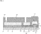
Fig. 1 is a cross-sectional view of a semiconductor device used in a first embodiment of the present invention. -
Fig. 2 is a cross-sectional view of the semiconductor device used in the first embodiment of the present invention, and the view illustrates a part different from one illustrated inFig. 1 . -
Fig. 3 is a cross-sectional view of the semiconductor device used in the first embodiment of the present invention, and the view illustrates the side close to a cell region. -
Fig. 4 is a cross-sectional view of a semiconductor device used in a second embodiment of the present invention. -
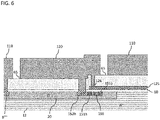
Fig. 5 is a cross-sectional view of a semiconductor device used in a third embodiment of the present invention. -
Fig. 6 is a cross-sectional view of the semiconductor device used in the third embodiment of the present invention, and the view illustrates a part different from one illustrated inFig. 5 . -
Fig. 7 is a cross-sectional view of a semiconductor device according to a fourth embodiment of the present invention based on an aspect according to the first embodiment. -
Fig. 8 is a cross-sectional view of the semiconductor device according to the fourth embodiment based on an aspect according to first embodiment, and the view illustrates a part different from one illustrated inFig. 7 . -
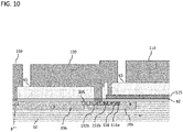
Fig. 9 is a cross-sectional view of a semiconductor device according to a fourth embodiment of the present invention based on an aspect according to the third embodiment. -
Fig. 10 is a cross-sectional view of the semiconductor device according to the fourth embodiment of the present invention based on an aspect according to the third embodiment, and the view illustrates a part different from one illustrated inFig. 9 . -
Fig. 11 is a cross-sectional view of a semiconductor device used in a fifth embodiment of the present invention. - In this embodiment, a vertical MOSFET will be described as an example. In this embodiment, a first conductivity type is described as n-type, and a second conductivity type is described as p-type. However, the present invention is not limited to such an aspect. The first conductivity type may be p-type, and the second conductivity type may be n-type. Furthermore, silicon carbide is employed as a wide gap semiconductor in this embodiment, but the present invention is not limited to such an aspect. Gallium nitride or the like may be employed as the wide gap semiconductor. In this embodiment, a direction perpendicular to a thickness direction or the vertical direction in
Fig. 1 is referred to as "in-plane direction." In other words, a plane including the horizontal direction and the normal direction ofFig. 1 is the "in-plane direction." - As illustrated in
Fig. 3 , a silicon carbide semiconductor device according to this embodiment may have an n-type siliconcarbide semiconductor substrate 11, adrift layer 12 provided on a first main surface (upper surface) of the siliconcarbide semiconductor substrate 11 and including an n-type silicon carbide material, a plurality of p-type well regions 20 provided in thedrift layer 12, and an n-type source region 30 provided in eachwell region 20. Thewell region 20 may be formed by, for example, implantation of a p-type impurity into thedrift layer 12. Thesource region 30 may be formed by, for example, implantation of an n-type impurity into thewell region 20. Adrain electrode 90 may be provided on a second main surface (lower surface) of the siliconcarbide semiconductor substrate 11. A withstand voltage structure may be provided outside a circumferential part of a region used as a cell. Thedrain electrode 90 may include, for example, titanium, aluminum, or nickel. - As illustrated in
Fig. 1 , the silicon carbide semiconductor device may have agate contact region 103 provided in thewell region 20 and electrically connected to agate pad 120, and aZener diode region 100 provided in thewell region 20 and between thesource region 30 and thegate contact region 103. Thegate contact region 103 and theZener diode region 100 may be formed by, for example, implantation of an n-type impurity or a p-type impurity into thewell region 20. - The
gate contact region 103 may be a superhigh-concentration n-type semiconductor region (n++) or a high-concentration p-type semiconductor region (n+). Thegate contact region 103 may be formed by contact between thegate pad 120 and the superhigh-concentration n-type semiconductor region (n++) or the high-concentration p-type semiconductor region (n+) through a gate contact hole provided in aninterlayer insulating film 65. In an aspect illustrated inFig. 1 , thegate contact region 103 is a superhigh-concentration n-type semiconductor region (n++), and the superhigh-concentration n-type semiconductor region (n++) is electrically connected to thegate pad 120. - As illustrated in
Fig. 2 , at a part other than thegate contact region 103, thegate pad 120 may be connected to agate electrode 125 so as to form agate connection region 126. Thegate connection region 126 may be formed by contact between thegate electrode 125 and thegate pad 120 via a gate contact hole provided in theinterlayer insulating film 65. - A
gate insulating film 60 is provided between thewell region 20 and theinterlayer insulating film 65. Thegate insulating film 60 may have a substantially uniform thickness. In other words, in this embodiment, a field insulating film which is typically provided below thegate pad 120 may not be employed. The "substantially uniform thickness" indicates that the thickness is within 10% of an average thickness D0 of thegate insulating film 60 and that the thickness of thegate insulating film 60 between thewell region 20 and theinterlayer insulating film 65 is 0.9 × D0 or more and 1.1 × D0 or less. - As illustrated in
Fig. 1 , thegate electrode 125 may be provided on thegate insulating film 60 between thesource regions 30. As illustrated inFig. 2 , thegate electrode 125 is electrically connected to thegate pad 120. - The
drift layer 12 may be formed on the first main surface of the siliconcarbide semiconductor substrate 11 by CVD or the like. Thedrift layer 12 may have a lower n-type impurity concentration than that of the siliconcarbide semiconductor substrate 11. Thedrift layer 12 may have a low-concentration region (n-), and the siliconcarbide semiconductor substrate 11 may have a higher concentration than that of thedrift layer 12. - N and P, for example, are employable as the n-type impurity, and Al and B, for example, are employable as the p-type impurity. The low-concentration region (n-), or the
drift layer 12 in this embodiment, has an impurity concentration of, for example, 1 × 10¹⁴ to 4 × 1016 cm-3. The siliconcarbide semiconductor substrate 11 has an impurity concentration of, for example, 1 × 10¹⁸ to 3 × 1019 cm-3. - The
gate pad 120 may include a metal such as Al, and thegate electrode 125 may be formed of, for example, polysilicon. Theinterlayer insulating film 65 may be formed on the upper surface of thegate electrode 125 and the like. Thegate electrode 125 may be formed by, for example, CVD or photolithography. Theinterlayer insulating film 65 may be formed by CVD or the like and may include, for example, silicon dioxide. - As illustrated in
Fig. 1 , theZener diode region 100 may have the aforementioned superhigh-concentration p-type semiconductor region (p++) 102 and high-concentration n-type semiconductor region (n+) 101 adjacent to the superhigh-concentration p-type semiconductor region 102. Thegate contact region 103 may be adjacent to the high-concentration n-type semiconductor region 101. A high-concentration n-type region (n+) in this embodiment has an impurity concentration of, for example, 1 × 10¹⁸ to 2 × 1019 cm-3, and a superhigh-concentration n-type region (n++) has an impurity concentration of, for example, 2 × 10¹⁹ to 1 × 1021 cm-3. Thewell region 20 in this embodiment has an impurity concentration of, for example, 5 × 10¹⁶ to 1 × 1019 cm-3. A superhigh-concentration p-type region (p++) has an impurity concentration of, for example, 2 × 10¹⁹ to 1 × 1021 cm-3, and a high-concentration p-type region (p+) has an impurity concentration of, for example, 3 × 10¹⁷ to 2 × 1019 cm-3. - Each of the superhigh-concentration p-
type semiconductor region 102, the high-concentration n-type semiconductor region 101, and thegate contact region 103 may have substantially equal depths. In this embodiment, the "substantially equal depths" indicates that each depth is within 10% of an average depth. Accordingly, the superhigh-concentration p-type semiconductor region 102, the high-concentration n-type semiconductor region 101, and thegate contact region 103 being substantially equal in depth indicates that these are within 10% of an average depth H0 of the superhigh-concentration p-type semiconductor region 102, the high-concentration n-type semiconductor region 101 and thegate contact region 103, and each of the superhigh-concentration p-type semiconductor region 102, the high-concentration n-type semiconductor region 101 and thegate contact region 103 has a depth of 0.9 × H0 or more and 1.1 × H0 or less. - Furthermore, the superhigh-concentration p-
type semiconductor region 102, the high-concentration n-type semiconductor region 101, and thegate contact region 103 each may have a depth substantially equal to those of a high-concentration n-type region 31 and a superhigh-concentration n-type region 32 of thesource region 30. - A depth of the
well region 20 is set so that a bottom surface of thewell region 20 is higher than a bottom surface of thedrift layer 12, which indicates that thewell region 20 is provided in thedrift layer 12. In addition, a depth of thesource region 30 is set so that a bottom surface of thesource region 30 is higher than the bottom surface of thewell region 20, which indicates that thesource region 30 is formed in thewell region 20. Depths of thegate contact region 103 and theZener diode region 100 are set so that bottom surfaces of those regions are higher than the bottom surface of thewell region 20, which indicates that thegate contact region 103 and theZener diode region 100 are formed in thewell region 20. - In the
source region 30, a part connected to thesource pad 110 may be a superhigh-concentration n-type region (n++), and a high-concentration n-type region (n+) may be adjacent to the superhigh-concentration n-type region (n++) . - The
Zener diode region 100 as in this embodiment may be provided not only around thegate pad 120 but also around a gate runner (not illustrated) or a wire relative to the gate electrode provided on theinterlayer insulating film 65 along whole or part of a circumferential part of a cell region. The present invention is not limited to such an aspect, and theZener diode region 100 as in this embodiment may be provided only around thegate pad 120 or may be provided only around the gate runner. - As illustrated in
Fig. 1 , thesource region 30 may have the high-concentration n-type region (n+) 31 provided on the side closer to thegate electrode 125 and the superhigh-concentration n-type region (n++) 32 adjacent to the high-concentration n-type region (n+) 31. In addition, the superhigh-concentration p-type semiconductor region 102 of theZener diode region 100 may be adjacent to the superhigh-concentration n-type region (n++) 32. Between thesource pad 110 and the superhigh-concentration n-type region (n++) 32 of thesource region 30 and between thesource pad 110 and the superhigh-concentration p-type semiconductor region 102 of theZener diode region 100, ametallic layer 40 including nickel, titanium, or an alloy containing nickel or titanium may be provided. - The superhigh-concentration n-type region (n++) 32 of the
source region 30 may come into contact with themetallic layer 40 provided below thesource pad 110 by an ohmic contact. Furthermore, the superhigh-concentration p-type semiconductor region 102 may come into contact with themetallic layer 40 provided below thesource pad 110 by an ohmic contact. - As illustrated in
Fig. 3 , awell contact region 21 that is in contact with themetallic layer 40 may be provided between thesource regions 30 in the plane direction. Thewell contact region 21 may include a superhigh-concentration p-type semiconductor. Thewell contact region 21 and themetallic layer 40 may be in contact with each other by an ohmic contact. Thewell contact region 21 may be formed by, for example, implantation of a p-type impurity into thewell region 20. - Next, examples of operation and effect of the present embodiment having the above-described configuration will be described. Note that all aspects described in "Operation and Effects" can be adopted in the above-described configuration.
- In this embodiment, as illustrated in
Fig. 1 , in an aspect where theZener diode region 100 is provided between thesource region 30 and thegate contact region 103, it is possible to prevent reduction in charge/discharge rate and to protect thegate insulating film 60. - In a case where the
Zener diode region 100 has the superhigh-concentration p-type semiconductor region (p++) 102 and the high-concentration n-type semiconductor region (n+) 101 adjacent to the superhigh-concentration p-type semiconductor region (p++) 102 and where the high-concentration n-type semiconductor region 101 has a higher n-type impurity concentration than a p-type impurity concentration in thewell region 20, a withstand voltage is determined by a junction between the superhigh-concentration p-type semiconductor region 102 and the high-concentration n-type semiconductor region 101. In a wide gap semiconductor such as silicon carbide, even when such a high-concentration region has only one junction, it is possible to apply a sufficient positive bias to a gate and to provide a withstand voltage (for example, 15 to 40 V) preferable for protecting the gate from an excessive positive bias. For example, with 4H-SiC, when the high-concentration n-type semiconductor region (n+) 101 has an impurity concentration of 2.5 × 1018 cm-3 and the superhigh-concentration p-type semiconductor region (p++) 102 has a sufficiently higher impurity concentration (for example, at 2 × 1020 cm-3), a withstand voltage obtained by device simulation is about 30 V. - Furthermore, in a case where the
Zener diode region 100 is provided as in this embodiment, a thickness of thewell region 20 is increased to such an extent that a parasitic bipolar transistor does not operate, which makes it possible to transfer part of junction capacitance between thedrift layer 12 and thewell region 20 to Crss (reverse transfer capacitance). Accordingly, it is possible to perform passive mirror operation and to prevent dV/dt from increasing more than necessary. - In this embodiment, as illustrated in
Fig. 2 , in an aspect where thegate insulating film 60 between thewell region 20 and theinterlayer insulating film 65 has a substantially uniform thickness and where no field insulating film is provided, it is possible to prevent a decrease of a gate withstand voltage. In other words, in a case where a field insulating film is provided and thegate insulating film 60 is provided on the field insulating film, a step is formed in thegate insulating film 60. Such a step decreases a gate withstand voltage. On the other hand, in an aspect where thegate insulating film 60 has a substantially uniform thickness and where no field insulating film is provided, such a step is not formed in the first place, which makes it possible to prevent a decrease of a gate withstand voltage. - Hereinafter, a second embodiment of the present invention will be described.
- In this embodiment, as illustrated in
Fig. 4 , awell region 20 provided with aZener diode region 100 and awell region 20 provided with asource region 30 are separated in the plane direction. Other configurations are similar to those of the first embodiment. The second embodiment can employ any configuration employed in the first embodiment. The members described in the first embodiment are described with the same reference numerals. - As described in the first embodiment, in a case where the
Zener diode region 100 is provided as in this embodiment, an increase in thickness of thewell region 20 makes it possible to transfer part of junction capacitance between theZener diode region 100 and thewell region 20 to Crss (reverse transfer capacitance) and to perform passive mirror operation. Performing such passive mirror operation is advantageous in that thewell region 20 provided with a superhigh-concentration p-type semiconductor region 102 of theZener diode region 100 and thesource region 30 is separated. In this case, as illustrated inFig. 4 , the superhigh-concentration p-type semiconductor region 102 of theZener diode region 100 and thewell region 20 provided with awell contact region 21 adjacent to thesource region 30 may be separated in the plane direction. - Hereinafter, a third embodiment of the present invention will be described.
- In this embodiment, as illustrated in
Fig. 5 , a planarsecondary MOSFET region 150 is provided in awell region 20. Thesecondary MOSFET region 150 has a pair of n-type semiconductor regions type semiconductor region 156 provided between the pair of n-type semiconductor regions MOSFET gate electrode 159. The secondaryMOSFET gate electrode 159 is provided on the n-type semiconductor regions type semiconductor region 156 via agate insulating film 60 serving as a secondary MOSFET insulating layer and is electrically connected to agate pad 120. The third embodiment can employ any configuration employed in each of the above embodiments. The members described in the above embodiments are described with the same reference numerals. In an aspect illustrated inFig. 5 , one of the pair of n-type semiconductor regions type semiconductor regions source pad 110, and the other has n-type semiconductor regions gate pad 120. - The n-
type semiconductor regions secondary MOSFET region 150 may have high-concentration n-type regions (n+) 151a and 151b and superhigh-concentration n-type regions (n++) 152a and 152b having a higher impurity concentration than that of the high-concentration n-type regions type region 152a may come into contact with thesource pad 110 via ametallic layer 40 to form a source contact region, and the other superhigh-concentration n-type region 152b may come into contact with thegate pad 120 to form a gate contact region. The p-type semiconductor region 156 of thesecondary MOSFET region 150 may be a high-concentration p-type semiconductor region (p+). A threshold voltage of the secondary MOSFET is required to be higher than a positive bias to be applied to a gate of a cell. Accordingly, in a case where at least thegate insulating film 60 of the secondary MOSFET is substantially equal to the cell in thickness, the p-type semiconductor region 156 is required to have a higher impurity concentration than that of thewell region 20. - As illustrated in
Fig. 6 , agate electrode 125 and thegate pad 120 are electrically connected via agate connection region 126. Thisgate electrode 125 may be electrically connected to the secondaryMOSFET gate electrode 159 illustrated inFig. 5 . Furthermore, thegate electrode 125 and the secondaryMOSFET gate electrode 159 may be formed in an integrated manner. - In regard to depths of the n-
type semiconductor regions type semiconductor region 156 of thesecondary MOSFET region 150, bottom surfaces thereof are placed higher than a bottom surface of thewell region 20. Thus, the n-type semiconductor regions type semiconductor region 156 of thesecondary MOSFET region 150 are formed in thewell region 20. Each of the n-type semiconductor regions type semiconductor region 156 of thesecondary MOSFET region 150 may be formed by, for example, implantation of an n-type impurity or a p-type impurity into thewell region 20. - The n-
type semiconductor regions type semiconductor region 156 may have a substantially equal depth. Furthermore, the n-type semiconductor regions type semiconductor region 156; and the high-concentration n-type region 31 and the superhigh-concentration n-type region 32 of thesource region 30 may have a substantially equal depth. - The
secondary MOSFET region 150 as in this embodiment may be provided not only around thegate pad 120 but also around a gate runner. The present invention is not limited to such an aspect, and thesecondary MOSFET region 150 as in this embodiment may be provided only around thegate pad 120 or may be provided only around the gate runner. - Furthermore, both the
Zener diode region 100 as described in each of the embodiments and thesecondary MOSFET region 150 in this embodiment may be employed, and theZener diode region 100 and thesecondary MOSFET region 150 are may be provided around thegate pad 120 and around the gate runner. Still further, both theZener diode region 100 and thesecondary MOSFET region 150 may be provided only around thegate pad 120 or may be provided only around the gate runner. Alternatively, one of theZener diode region 100 and thesecondary MOSFET region 150 may be provided only around thegate pad 120, and the other may be provided only around the gate runner. - Hereinafter, a fourth embodiment of the present invention will be described.
- In this embodiment, as illustrated in
Figs. 7 to 10 , awell region 20 has afirst well region 20a provided below a part of agate pad 120 and asecond well region 20b separated from thefirst well region 20a in the plane direction. The fourth embodiment can employ any configuration employed in each of the above embodiments. The members described in the above embodiments are described with the same reference numerals. In an aspect illustrated inFig. 7 , aZener diode region 100 is provided in thefirst well region 20a. In an aspect illustrated inFig. 9 , a part of asecondary MOSFET region 150 is provided in thefirst well region 20a. - In a case where a potential of the
well region 20 rises due to a displacement current that charges large junction capacitance between adrift layer 12 below thegate pad 120 and thewell region 20 during switching, a large current sometimes flows through agate electrode 125. In this case, dV/dt is significantly limited. For this reason, as in this embodiment, it is favorable to separate thefirst well region 20a and thesecond well region 20b, to cover a large part of the region below the gate pad 120 (for example, 80% or more in the region in the plane direction) with thesecond well region 20b, and to separate thesecond well region 20b from a cell region and from thefirst well region 20a provided with theZener diode region 100 or thesecondary MOSFET region 150. In this manner, thefirst well region 20a and thesecond well region 20b are separated so as to prevent significant limitation of dV/dt. - As illustrated in
Figs. 7 to 10 , aseparation region 105 being an n-type semiconductor having a higher impurity concentration than adrift layer 12 may be provided between thefirst well region 20a and thesecond well region 20b. Due to theseparation region 105 that includes the n-type semiconductor having a higher impurity concentration than that of thedrift layer 12, it is possible to separate thefirst well region 20a and thesecond well region 20b more reliably. Theseparation region 105 may be formed by, for example, implantation of an n-type impurity around a gap of thewell region 20. Theseparation region 105 has an impurity concentration of, for example, 5 × 10¹⁶ to 5 × 1017 cm-3. - Hereinafter, a fifth embodiment of the present invention will be described.
- In this embodiment, in a case where the
Zener diode region 100 according to the first embodiment, the second embodiment or the fourth embodiment is employed, a high-concentration n-type region (n+) 103a is employed as a gate contact region, and thegate contact region 103a is brought into contact with thegate pad 120 by a Schottky contact, instead of employing a superhigh-concentration n-type region (n++) as a gate contact region and bringing the gate contact region into contact with thegate pad 120 by an ohmic contact. Furthermore, a part of thegate contact region 103a excluding an end has an n-type impurity concentration lower than a p-type impurity concentration of thewell region 20, and the part may be, for example, a low-concentration n-type region (n-) 109. The fifth embodiment can employ any configuration employed in each of the above embodiments. The members described in the above embodiments are described with the same reference numerals. - Employing a high-concentration n-type region (n+) as the
gate contact region 103a and bringing thegate contact region 103a into contact with thegate pad 120 by a Schottky contact enable application of a negative bias (for example, -3 V or lower) equal to or more than the built-in voltage of a pn diode. - Furthermore, as illustrated in
Fig. 11 , in an aspect where thegate contact region 103a is separated by the low-concentration n-type region 109, it is possible to deplete a part of thegate contact region 103a excluding an end and to prevent Ciss (input capacitance) from increasing excessively. - The description of each embodiment, the description of the modification, and the disclosure of the drawings described above are merely examples for explaining the invention described in the claims, and the invention described in the claims is not limited by the description of the embodiment or the disclosure of the drawings described above. In addition, the recitation of the claims at the original application is merely an example, and the description of the claims can be appropriately changed based on the description of the specification, the drawings, and the like.
-
- 12 Drift layer
- 20 Well region
- 20a First well region
- 20b Second well region
- 30 Source region
- 60 Gate insulating film
- 100 Zener diode region
- 101 High-concentration first conductivity type semiconductor region
- 102 Superhigh-concentration second conductivity type semiconductor region
- 103 Gate contact region
- 105 Separation region
- 120 Gate pad
- 125 Secondary MOSFET gate electrode
- 150 Secondary MOSFET region
- 151a, 151b, 152a, 152b n-type semiconductor region
- 156 p-type semiconductor region
- 159 Secondary MOSFET gate electrode
Claims (5)
- A wide band gap semiconductor device comprising:a drain electrode;a drift layer being a first conductivity type and provided above the drain electrode;a well region being a second conductivity type and provided in the drift layer;a source region being a first conductivity type and provided in the well region;a gate electrode electrically connected to a gate pad;a secondary MOSFET region provided in the well region,an interlayer insulating film (65); anda gate insulating film (60) provided between the well region (20) and the interlayer insulating film (65), whereinthe secondary MOSFET region has a pair of first conductivity type semiconductor regions, a second conductivity type semiconductor region provided between the pair of the first conductivity type semiconductor regions, and a secondary MOSFET gate electrode, which is provided on the first conductivity type semiconductor regions and the second conductivity type semiconductor region via a secondary MOSFET insulating layer and which is electrically connected to a gate pad,one of the first conductivity type semiconductor regions is electrically connected to a source pad, andthe other of the first conductivity type semiconductor regions is electrically connected to a gate pad.
- The wide band gap semiconductor device according to claim 1, whereinthe first conductivity type semiconductor region has a high-concentration first conductivity type region, andthe second conductivity type semiconductor region has a high-concentration second conductivity type region.
- The wide band gap semiconductor device according to claim 1, whereinthe well region has a first well region provided below a part of the gate pad and a second well region separated from the first well region,the secondary MOSFET region is provided in the first well region.
- The wide band gap semiconductor device according to claim 3, wherein
a separation region, being a first conductivity type semiconductor and having a higher impurity concentration than the drift layer, is provided between the first well region and the second well region. - The wide gap semiconductor device, according to claim 1, wherein the gate insulating film has a substantially uniform thickness.
Priority Applications (1)
| Application Number | Priority Date | Filing Date | Title |
|---|---|---|---|
| EP22162506.4A EP4036990A1 (en) | 2017-11-13 | 2017-11-13 | Wide gap semiconductor device |
Applications Claiming Priority (3)
| Application Number | Priority Date | Filing Date | Title |
|---|---|---|---|
| EP17931382.0A EP3712957B1 (en) | 2017-11-13 | 2017-11-13 | Wide band gap semiconductor device |
| EP22162506.4A EP4036990A1 (en) | 2017-11-13 | 2017-11-13 | Wide gap semiconductor device |
| PCT/JP2017/040677 WO2019092872A1 (en) | 2017-11-13 | 2017-11-13 | Wide gap semiconductor device |
Related Parent Applications (2)
| Application Number | Title | Priority Date | Filing Date |
|---|---|---|---|
| EP17931382.0A Division EP3712957B1 (en) | 2017-11-13 | 2017-11-13 | Wide band gap semiconductor device |
| EP17931382.0A Division-Into EP3712957B1 (en) | 2017-11-13 | 2017-11-13 | Wide band gap semiconductor device |
Publications (1)
| Publication Number | Publication Date |
|---|---|
| EP4036990A1 true EP4036990A1 (en) | 2022-08-03 |
Family
ID=66438362
Family Applications (2)
| Application Number | Title | Priority Date | Filing Date |
|---|---|---|---|
| EP17931382.0A Active EP3712957B1 (en) | 2017-11-13 | 2017-11-13 | Wide band gap semiconductor device |
| EP22162506.4A Pending EP4036990A1 (en) | 2017-11-13 | 2017-11-13 | Wide gap semiconductor device |
Family Applications Before (1)
| Application Number | Title | Priority Date | Filing Date |
|---|---|---|---|
| EP17931382.0A Active EP3712957B1 (en) | 2017-11-13 | 2017-11-13 | Wide band gap semiconductor device |
Country Status (5)
| Country | Link |
|---|---|
| US (1) | US11437506B2 (en) |
| EP (2) | EP3712957B1 (en) |
| JP (1) | JP7051890B2 (en) |
| CN (1) | CN111295763B (en) |
| WO (1) | WO2019092872A1 (en) |
Families Citing this family (6)
| Publication number | Priority date | Publication date | Assignee | Title |
|---|---|---|---|---|
| JP7295047B2 (en) * | 2020-01-22 | 2023-06-20 | 株式会社東芝 | semiconductor equipment |
| JP2022012503A (en) * | 2020-07-01 | 2022-01-17 | ローム株式会社 | Semiconductor device |
| KR102878956B1 (en) * | 2020-09-03 | 2025-10-30 | 에스케이하이닉스 주식회사 | image sensing device |
| JP7643179B2 (en) * | 2021-05-24 | 2025-03-11 | 富士電機株式会社 | Silicon carbide semiconductor device |
| JP7570299B2 (en) * | 2021-08-02 | 2024-10-21 | 三菱電機株式会社 | Silicon carbide semiconductor device and method for manufacturing silicon carbide semiconductor device |
| CN115632031B (en) * | 2022-12-21 | 2023-03-28 | 泰科天润半导体科技(北京)有限公司 | Manufacturing method of planar gate silicon carbide MOSFET with integrated gate protection mechanism |
Citations (2)
| Publication number | Priority date | Publication date | Assignee | Title |
|---|---|---|---|---|
| JP2012064727A (en) | 2010-09-15 | 2012-03-29 | Rohm Co Ltd | Semiconductor device |
| US20150008450A1 (en) * | 2013-07-04 | 2015-01-08 | Mitsubishi Electric Corporation | Wide band gap semiconductor device |
Family Cites Families (20)
| Publication number | Priority date | Publication date | Assignee | Title |
|---|---|---|---|---|
| JPS6337846A (en) | 1986-07-31 | 1988-02-18 | Canon Inc | Cassette loading device |
| US5172290A (en) * | 1988-08-10 | 1992-12-15 | Siemens Aktiengesellschaft | Gate-source protective circuit for a power mosfet |
| JPH03129779A (en) | 1989-07-12 | 1991-06-03 | Fuji Electric Co Ltd | Semiconductor device having high breakdown strength |
| FR2649828B1 (en) * | 1989-07-17 | 1991-10-31 | Sgs Thomson Microelectronics | VDMOS / LOGIC INTEGRATED CIRCUIT COMPRISING A DEPLETED VERTICAL TRANSISTOR AND A ZENER DIODE |
| DE69325645T2 (en) * | 1993-04-21 | 1999-12-09 | Consorzio Per La Ricerca Sulla Microelettronica Nel Mezzogiorno, Catania | Integrated protection circuit structure for the protection of logic MOS power semiconductor components from electrostatic discharges |
| JPH08288526A (en) | 1995-04-12 | 1996-11-01 | Oki Electric Ind Co Ltd | Semiconductor device |
| US5602046A (en) * | 1996-04-12 | 1997-02-11 | National Semiconductor Corporation | Integrated zener diode protection structures and fabrication methods for DMOS power devices |
| KR100275758B1 (en) * | 1998-12-17 | 2001-02-01 | 김덕중 | Horizontal Morse Gate Semiconductor Device with Zener Diode and Manufacturing Method Thereof |
| US6580101B2 (en) * | 2000-04-25 | 2003-06-17 | The Furukawa Electric Co., Ltd. | GaN-based compound semiconductor device |
| JP4462030B2 (en) | 2004-12-22 | 2010-05-12 | 富士電機システムズ株式会社 | Semiconductor device |
| JP4955222B2 (en) * | 2005-05-20 | 2012-06-20 | ルネサスエレクトロニクス株式会社 | Manufacturing method of semiconductor device |
| JP2009004399A (en) | 2007-06-19 | 2009-01-08 | Rohm Co Ltd | Semiconductor device |
| WO2008153142A1 (en) | 2007-06-15 | 2008-12-18 | Rohm Co., Ltd. | Semiconductor device |
| CN101226962B (en) * | 2008-02-22 | 2013-07-17 | 苏州赛芯电子科技有限公司 | HVMOS and semiconductor device integrating HVMOS and CMOS |
| JP2009218307A (en) * | 2008-03-10 | 2009-09-24 | Fuji Electric Device Technology Co Ltd | Mos-type semiconductor device |
| JP5340018B2 (en) | 2009-05-01 | 2013-11-13 | 三菱電機株式会社 | Semiconductor device |
| CN103329256B (en) | 2010-12-15 | 2016-09-21 | 宜普电源转换公司 | There is the semiconductor device of rear surface isolation |
| JP6037499B2 (en) * | 2011-06-08 | 2016-12-07 | ローム株式会社 | Semiconductor device and manufacturing method thereof |
| US20130187195A1 (en) * | 2012-01-24 | 2013-07-25 | Infineon Technologies Austria Ag | Power Transistor |
| JP2015159235A (en) * | 2014-02-25 | 2015-09-03 | 住友電気工業株式会社 | Semiconductor device |
-
2017
- 2017-11-13 CN CN201780096412.1A patent/CN111295763B/en active Active
- 2017-11-13 JP JP2019551851A patent/JP7051890B2/en active Active
- 2017-11-13 EP EP17931382.0A patent/EP3712957B1/en active Active
- 2017-11-13 EP EP22162506.4A patent/EP4036990A1/en active Pending
- 2017-11-13 US US16/763,550 patent/US11437506B2/en active Active
- 2017-11-13 WO PCT/JP2017/040677 patent/WO2019092872A1/en not_active Ceased
Patent Citations (2)
| Publication number | Priority date | Publication date | Assignee | Title |
|---|---|---|---|---|
| JP2012064727A (en) | 2010-09-15 | 2012-03-29 | Rohm Co Ltd | Semiconductor device |
| US20150008450A1 (en) * | 2013-07-04 | 2015-01-08 | Mitsubishi Electric Corporation | Wide band gap semiconductor device |
Also Published As
| Publication number | Publication date |
|---|---|
| JPWO2019092872A1 (en) | 2020-11-12 |
| EP3712957A1 (en) | 2020-09-23 |
| EP3712957A4 (en) | 2021-09-29 |
| EP3712957B1 (en) | 2022-12-14 |
| CN111295763A (en) | 2020-06-16 |
| CN111295763B (en) | 2023-12-29 |
| WO2019092872A1 (en) | 2019-05-16 |
| JP7051890B2 (en) | 2022-04-11 |
| US11437506B2 (en) | 2022-09-06 |
| US20210376142A1 (en) | 2021-12-02 |
Similar Documents
| Publication | Publication Date | Title |
|---|---|---|
| EP3712957B1 (en) | Wide band gap semiconductor device | |
| US10714609B2 (en) | Semiconductor device with stripe-shaped trench gate structures, transistor mesas and diode mesas | |
| US9947741B2 (en) | Field-effect semiconductor device having pillar regions of different conductivity type arranged in an active area | |
| US9923066B2 (en) | Wide bandgap semiconductor device | |
| JP5517688B2 (en) | Semiconductor device | |
| JP2016009712A (en) | Silicon carbide semiconductor device | |
| US10573731B2 (en) | Semiconductor transistor and method for forming the semiconductor transistor | |
| US11387359B2 (en) | Ppower semiconductor device with anticorrosive edge termination structure | |
| US9178021B1 (en) | Silicon carbide semiconductor device | |
| US11309415B2 (en) | Wide gap semiconductor device | |
| US10957764B2 (en) | Vertical semiconductor device | |
| US10770579B2 (en) | SiC-MOSFET and method of manufacturing the same | |
| WO2017002255A1 (en) | Semiconductor device | |
| JP2015159235A (en) | Semiconductor device | |
| CN108231868B (en) | Field-effect semiconductor component and method for producing the same | |
| US20160005811A1 (en) | Charge compensation device and manufacturing therefor | |
| JP2013219207A (en) | Semiconductor device for electric power and manufacturing method of the same | |
| US11251266B2 (en) | Power semiconductor device and method of processing a power semiconductor device | |
| CN110660795A (en) | Power semiconductor device |
Legal Events
| Date | Code | Title | Description |
|---|---|---|---|
| PUAI | Public reference made under article 153(3) epc to a published international application that has entered the european phase |
Free format text: ORIGINAL CODE: 0009012 |
|
| STAA | Information on the status of an ep patent application or granted ep patent |
Free format text: STATUS: REQUEST FOR EXAMINATION WAS MADE |
|
| 17P | Request for examination filed |
Effective date: 20220316 |
|
| AC | Divisional application: reference to earlier application |
Ref document number: 3712957 Country of ref document: EP Kind code of ref document: P |
|
| AK | Designated contracting states |
Kind code of ref document: A1 Designated state(s): AL AT BE BG CH CY CZ DE DK EE ES FI FR GB GR HR HU IE IS IT LI LT LU LV MC MK MT NL NO PL PT RO RS SE SI SK SM TR |