EP4036641A1 - Elektronische vorrichtung und verfahren zu deren steuerung und computerlesbares speichermedium - Google Patents
Elektronische vorrichtung und verfahren zu deren steuerung und computerlesbares speichermedium Download PDFInfo
- Publication number
- EP4036641A1 EP4036641A1 EP20869950.4A EP20869950A EP4036641A1 EP 4036641 A1 EP4036641 A1 EP 4036641A1 EP 20869950 A EP20869950 A EP 20869950A EP 4036641 A1 EP4036641 A1 EP 4036641A1
- Authority
- EP
- European Patent Office
- Prior art keywords
- liquid crystal
- movable
- camera
- electronic device
- backlight
- Prior art date
- Legal status (The legal status is an assumption and is not a legal conclusion. Google has not performed a legal analysis and makes no representation as to the accuracy of the status listed.)
- Granted
Links
Images

Classifications
-
- G—PHYSICS
- G02—OPTICS
- G02F—OPTICAL DEVICES OR ARRANGEMENTS FOR THE CONTROL OF LIGHT BY MODIFICATION OF THE OPTICAL PROPERTIES OF THE MEDIA OF THE ELEMENTS INVOLVED THEREIN; NON-LINEAR OPTICS; FREQUENCY-CHANGING OF LIGHT; OPTICAL LOGIC ELEMENTS; OPTICAL ANALOGUE/DIGITAL CONVERTERS
- G02F1/00—Devices or arrangements for the control of the intensity, colour, phase, polarisation or direction of light arriving from an independent light source, e.g. switching, gating or modulating; Non-linear optics
- G02F1/01—Devices or arrangements for the control of the intensity, colour, phase, polarisation or direction of light arriving from an independent light source, e.g. switching, gating or modulating; Non-linear optics for the control of the intensity, phase, polarisation or colour
- G02F1/13—Devices or arrangements for the control of the intensity, colour, phase, polarisation or direction of light arriving from an independent light source, e.g. switching, gating or modulating; Non-linear optics for the control of the intensity, phase, polarisation or colour based on liquid crystals, e.g. single liquid crystal display cells
- G02F1/133—Constructional arrangements; Operation of liquid crystal cells; Circuit arrangements
- G02F1/1333—Constructional arrangements; Manufacturing methods
- G02F1/133371—Cells with varying thickness of the liquid crystal layer
-
- G—PHYSICS
- G02—OPTICS
- G02F—OPTICAL DEVICES OR ARRANGEMENTS FOR THE CONTROL OF LIGHT BY MODIFICATION OF THE OPTICAL PROPERTIES OF THE MEDIA OF THE ELEMENTS INVOLVED THEREIN; NON-LINEAR OPTICS; FREQUENCY-CHANGING OF LIGHT; OPTICAL LOGIC ELEMENTS; OPTICAL ANALOGUE/DIGITAL CONVERTERS
- G02F1/00—Devices or arrangements for the control of the intensity, colour, phase, polarisation or direction of light arriving from an independent light source, e.g. switching, gating or modulating; Non-linear optics
- G02F1/01—Devices or arrangements for the control of the intensity, colour, phase, polarisation or direction of light arriving from an independent light source, e.g. switching, gating or modulating; Non-linear optics for the control of the intensity, phase, polarisation or colour
- G02F1/13—Devices or arrangements for the control of the intensity, colour, phase, polarisation or direction of light arriving from an independent light source, e.g. switching, gating or modulating; Non-linear optics for the control of the intensity, phase, polarisation or colour based on liquid crystals, e.g. single liquid crystal display cells
- G02F1/133—Constructional arrangements; Operation of liquid crystal cells; Circuit arrangements
- G02F1/1333—Constructional arrangements; Manufacturing methods
-
- G—PHYSICS
- G02—OPTICS
- G02F—OPTICAL DEVICES OR ARRANGEMENTS FOR THE CONTROL OF LIGHT BY MODIFICATION OF THE OPTICAL PROPERTIES OF THE MEDIA OF THE ELEMENTS INVOLVED THEREIN; NON-LINEAR OPTICS; FREQUENCY-CHANGING OF LIGHT; OPTICAL LOGIC ELEMENTS; OPTICAL ANALOGUE/DIGITAL CONVERTERS
- G02F1/00—Devices or arrangements for the control of the intensity, colour, phase, polarisation or direction of light arriving from an independent light source, e.g. switching, gating or modulating; Non-linear optics
- G02F1/01—Devices or arrangements for the control of the intensity, colour, phase, polarisation or direction of light arriving from an independent light source, e.g. switching, gating or modulating; Non-linear optics for the control of the intensity, phase, polarisation or colour
- G02F1/13—Devices or arrangements for the control of the intensity, colour, phase, polarisation or direction of light arriving from an independent light source, e.g. switching, gating or modulating; Non-linear optics for the control of the intensity, phase, polarisation or colour based on liquid crystals, e.g. single liquid crystal display cells
- G02F1/133—Constructional arrangements; Operation of liquid crystal cells; Circuit arrangements
- G02F1/13306—Circuit arrangements or driving methods for the control of single liquid crystal cells
- G02F1/13312—Circuits comprising photodetectors for purposes other than feedback
-
- G—PHYSICS
- G02—OPTICS
- G02F—OPTICAL DEVICES OR ARRANGEMENTS FOR THE CONTROL OF LIGHT BY MODIFICATION OF THE OPTICAL PROPERTIES OF THE MEDIA OF THE ELEMENTS INVOLVED THEREIN; NON-LINEAR OPTICS; FREQUENCY-CHANGING OF LIGHT; OPTICAL LOGIC ELEMENTS; OPTICAL ANALOGUE/DIGITAL CONVERTERS
- G02F1/00—Devices or arrangements for the control of the intensity, colour, phase, polarisation or direction of light arriving from an independent light source, e.g. switching, gating or modulating; Non-linear optics
- G02F1/01—Devices or arrangements for the control of the intensity, colour, phase, polarisation or direction of light arriving from an independent light source, e.g. switching, gating or modulating; Non-linear optics for the control of the intensity, phase, polarisation or colour
- G02F1/13—Devices or arrangements for the control of the intensity, colour, phase, polarisation or direction of light arriving from an independent light source, e.g. switching, gating or modulating; Non-linear optics for the control of the intensity, phase, polarisation or colour based on liquid crystals, e.g. single liquid crystal display cells
- G02F1/133—Constructional arrangements; Operation of liquid crystal cells; Circuit arrangements
- G02F1/1333—Constructional arrangements; Manufacturing methods
- G02F1/133308—Support structures for LCD panels, e.g. frames or bezels
- G02F1/133331—Cover glasses
-
- G—PHYSICS
- G02—OPTICS
- G02F—OPTICAL DEVICES OR ARRANGEMENTS FOR THE CONTROL OF LIGHT BY MODIFICATION OF THE OPTICAL PROPERTIES OF THE MEDIA OF THE ELEMENTS INVOLVED THEREIN; NON-LINEAR OPTICS; FREQUENCY-CHANGING OF LIGHT; OPTICAL LOGIC ELEMENTS; OPTICAL ANALOGUE/DIGITAL CONVERTERS
- G02F1/00—Devices or arrangements for the control of the intensity, colour, phase, polarisation or direction of light arriving from an independent light source, e.g. switching, gating or modulating; Non-linear optics
- G02F1/01—Devices or arrangements for the control of the intensity, colour, phase, polarisation or direction of light arriving from an independent light source, e.g. switching, gating or modulating; Non-linear optics for the control of the intensity, phase, polarisation or colour
- G02F1/13—Devices or arrangements for the control of the intensity, colour, phase, polarisation or direction of light arriving from an independent light source, e.g. switching, gating or modulating; Non-linear optics for the control of the intensity, phase, polarisation or colour based on liquid crystals, e.g. single liquid crystal display cells
- G02F1/133—Constructional arrangements; Operation of liquid crystal cells; Circuit arrangements
- G02F1/1333—Constructional arrangements; Manufacturing methods
- G02F1/1335—Structural association of cells with optical devices, e.g. polarisers or reflectors
- G02F1/133509—Filters, e.g. light shielding masks
- G02F1/133514—Colour filters
-
- G—PHYSICS
- G02—OPTICS
- G02F—OPTICAL DEVICES OR ARRANGEMENTS FOR THE CONTROL OF LIGHT BY MODIFICATION OF THE OPTICAL PROPERTIES OF THE MEDIA OF THE ELEMENTS INVOLVED THEREIN; NON-LINEAR OPTICS; FREQUENCY-CHANGING OF LIGHT; OPTICAL LOGIC ELEMENTS; OPTICAL ANALOGUE/DIGITAL CONVERTERS
- G02F1/00—Devices or arrangements for the control of the intensity, colour, phase, polarisation or direction of light arriving from an independent light source, e.g. switching, gating or modulating; Non-linear optics
- G02F1/01—Devices or arrangements for the control of the intensity, colour, phase, polarisation or direction of light arriving from an independent light source, e.g. switching, gating or modulating; Non-linear optics for the control of the intensity, phase, polarisation or colour
- G02F1/13—Devices or arrangements for the control of the intensity, colour, phase, polarisation or direction of light arriving from an independent light source, e.g. switching, gating or modulating; Non-linear optics for the control of the intensity, phase, polarisation or colour based on liquid crystals, e.g. single liquid crystal display cells
- G02F1/133—Constructional arrangements; Operation of liquid crystal cells; Circuit arrangements
- G02F1/1333—Constructional arrangements; Manufacturing methods
- G02F1/1335—Structural association of cells with optical devices, e.g. polarisers or reflectors
- G02F1/133528—Polarisers
-
- G—PHYSICS
- G02—OPTICS
- G02F—OPTICAL DEVICES OR ARRANGEMENTS FOR THE CONTROL OF LIGHT BY MODIFICATION OF THE OPTICAL PROPERTIES OF THE MEDIA OF THE ELEMENTS INVOLVED THEREIN; NON-LINEAR OPTICS; FREQUENCY-CHANGING OF LIGHT; OPTICAL LOGIC ELEMENTS; OPTICAL ANALOGUE/DIGITAL CONVERTERS
- G02F1/00—Devices or arrangements for the control of the intensity, colour, phase, polarisation or direction of light arriving from an independent light source, e.g. switching, gating or modulating; Non-linear optics
- G02F1/01—Devices or arrangements for the control of the intensity, colour, phase, polarisation or direction of light arriving from an independent light source, e.g. switching, gating or modulating; Non-linear optics for the control of the intensity, phase, polarisation or colour
- G02F1/13—Devices or arrangements for the control of the intensity, colour, phase, polarisation or direction of light arriving from an independent light source, e.g. switching, gating or modulating; Non-linear optics for the control of the intensity, phase, polarisation or colour based on liquid crystals, e.g. single liquid crystal display cells
- G02F1/133—Constructional arrangements; Operation of liquid crystal cells; Circuit arrangements
- G02F1/1333—Constructional arrangements; Manufacturing methods
- G02F1/1335—Structural association of cells with optical devices, e.g. polarisers or reflectors
- G02F1/1336—Illuminating devices
-
- G—PHYSICS
- G02—OPTICS
- G02F—OPTICAL DEVICES OR ARRANGEMENTS FOR THE CONTROL OF LIGHT BY MODIFICATION OF THE OPTICAL PROPERTIES OF THE MEDIA OF THE ELEMENTS INVOLVED THEREIN; NON-LINEAR OPTICS; FREQUENCY-CHANGING OF LIGHT; OPTICAL LOGIC ELEMENTS; OPTICAL ANALOGUE/DIGITAL CONVERTERS
- G02F1/00—Devices or arrangements for the control of the intensity, colour, phase, polarisation or direction of light arriving from an independent light source, e.g. switching, gating or modulating; Non-linear optics
- G02F1/01—Devices or arrangements for the control of the intensity, colour, phase, polarisation or direction of light arriving from an independent light source, e.g. switching, gating or modulating; Non-linear optics for the control of the intensity, phase, polarisation or colour
- G02F1/13—Devices or arrangements for the control of the intensity, colour, phase, polarisation or direction of light arriving from an independent light source, e.g. switching, gating or modulating; Non-linear optics for the control of the intensity, phase, polarisation or colour based on liquid crystals, e.g. single liquid crystal display cells
- G02F1/133—Constructional arrangements; Operation of liquid crystal cells; Circuit arrangements
- G02F1/136—Liquid crystal cells structurally associated with a semi-conducting layer or substrate, e.g. cells forming part of an integrated circuit
- G02F1/1362—Active matrix addressed cells
- G02F1/1368—Active matrix addressed cells in which the switching element is a three-electrode device
-
- H—ELECTRICITY
- H04—ELECTRIC COMMUNICATION TECHNIQUE
- H04N—PICTORIAL COMMUNICATION, e.g. TELEVISION
- H04N23/00—Cameras or camera modules comprising electronic image sensors; Control thereof
- H04N23/57—Mechanical or electrical details of cameras or camera modules specially adapted for being embedded in other devices
-
- H—ELECTRICITY
- H04—ELECTRIC COMMUNICATION TECHNIQUE
- H04N—PICTORIAL COMMUNICATION, e.g. TELEVISION
- H04N23/00—Cameras or camera modules comprising electronic image sensors; Control thereof
- H04N23/60—Control of cameras or camera modules
-
- H—ELECTRICITY
- H04—ELECTRIC COMMUNICATION TECHNIQUE
- H04N—PICTORIAL COMMUNICATION, e.g. TELEVISION
- H04N23/00—Cameras or camera modules comprising electronic image sensors; Control thereof
- H04N23/70—Circuitry for compensating brightness variation in the scene
-
- H—ELECTRICITY
- H04—ELECTRIC COMMUNICATION TECHNIQUE
- H04N—PICTORIAL COMMUNICATION, e.g. TELEVISION
- H04N23/00—Cameras or camera modules comprising electronic image sensors; Control thereof
- H04N23/70—Circuitry for compensating brightness variation in the scene
- H04N23/75—Circuitry for compensating brightness variation in the scene by influencing optical camera components
-
- H—ELECTRICITY
- H04—ELECTRIC COMMUNICATION TECHNIQUE
- H04M—TELEPHONIC COMMUNICATION
- H04M1/00—Substation equipment, e.g. for use by subscribers
- H04M1/02—Constructional features of telephone sets
- H04M1/0202—Portable telephone sets, e.g. cordless phones, mobile phones or bar type handsets
- H04M1/026—Details of the structure or mounting of specific components
- H04M1/0264—Details of the structure or mounting of specific components for a camera module assembly
-
- H—ELECTRICITY
- H04—ELECTRIC COMMUNICATION TECHNIQUE
- H04M—TELEPHONIC COMMUNICATION
- H04M1/00—Substation equipment, e.g. for use by subscribers
- H04M1/02—Constructional features of telephone sets
- H04M1/0202—Portable telephone sets, e.g. cordless phones, mobile phones or bar type handsets
- H04M1/026—Details of the structure or mounting of specific components
- H04M1/0266—Details of the structure or mounting of specific components for a display module assembly
Definitions
- the present disclosure relates to the technical field of communications devices, and in particular, to an electronic device, a control method of the same, and a computer-readable storage medium.
- a camera that is disposed on a frame of a conventional device is disposed below a display module.
- the display module needs to be provided with a light-transmitting area. The camera senses ambient light through the light transmitting area, thereby implementing shooting.
- a display module usually includes a liquid crystal display and a backlight module.
- the liquid crystal display does not have a light-emitting function, so that the backlight module needs to provide backlight, thereby implementing a display function of the liquid crystal display.
- an area of the backlight module opposite to a camera needs to be designed to be a light-transmitting area; and an area of the liquid crystal display opposite to the camera also needs to be designed to be a light-transmitting area.
- light transmittance of the light-transmitting area impacts a shooting effect of the camera.
- an arrangement manner of liquid crystal particles in a liquid crystal layer of the liquid crystal display is controlled via an electric field, thereby displaying a picture.
- the liquid crystal layer is relatively thick, the light transmittance is affected. As a result, light-transmitting performance of the light-transmitting area is poor, which causes a poor shooting effect of the camera.
- a liquid crystal layer in an area, opposite to a light-transmitting area, of a liquid crystal display is hollowed out.
- the liquid crystal display has an area in which displaying cannot be performed.
- display performance of the electronic device is affected.
- appearance of the electronic device is also affected.
- the present disclosure discloses an electronic device, to resolve a problem that a part of a liquid crystal layer of a liquid crystal display is hollowed out, which further leads to poor display performance and poor appearance of the electronic device.
- an electronic device including a housing, a display module, a camera, and a drive structure, where the camera and the drive structure are disposed in an inner cavity formed by the display module and the housing;
- the present disclosure further provides a control method of an electronic device.
- the electronic device is the foregoing electronic device.
- the control method includes following steps:
- the present disclosure further provides an electronic device, including:
- the present disclosure further provides an electronic device, including a processor, a memory, and a computer program stored in the memory and executable on the processor, where when the computer program is executed by the processor, the foregoing control method is implemented.
- the present disclosure further provides a computer-readable storage medium.
- the computer-readable storage medium stores a computer program, and when the computer program is executed, the foregoing control method is implemented.
- a backlight module is divided into a fixed backlight component and a movable backlight component, and the movable backlight component can slide in a first sliding hole formed in the fixed backlight component.
- a second base assembly, disposed between a liquid crystal layer and a camera, of a liquid crystal display is designed to be a structure including a movable block, so that both the movable block and the movable backlight component are disposed opposite to the camera. The camera can shoot an image through the movable block, the movable backlight component, the liquid crystal layer, and the first base assembly.
- the drive structure can drive the camera to move towards the movable backlight component, so that the camera drives the movable backlight component and the movable block to squeeze the liquid crystal layer.
- Liquid crystal particles in the liquid crystal layer deform or move after being squeezed, so that an area of the liquid crystal layer squeezed by the movable block becomes thinner, thereby allowing more light to sequentially penetrate through the movable block and the movable backlight component after passing through the thinned area, to enter the camera. Therefore, shooting requirements of the camera can be better met.
- the shooting quality of the foregoing camera can be improved, so that liquid crystal particles in an area, opposite to the camera, of the liquid crystal layer do not need to be hollowed out. Therefore, impacts on display performance and appearance of the electronic device can be avoided.
- the embodiments of the present disclosure disclose an electronic device.
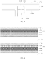
- the disclosed electronic device includes a housing, a display module 100, a camera 200, and a drive structure 300.
- the housing is a basic component of the electronic device and can provide a mounting foundation for other components of the electronic device.
- all of the display module 100, the camera 200, and the drive structure 300 are directly or indirectly mounted in the housing.
- the display module 100 is a display structural member of the electronic device, and can implement presentation of display content.
- the display module 100 is mounted on the housing. In a specific implementation, the display module 100 may be fixed on the housing in a bonding manner.
- the display module 100 and the housing form an inner cavity.
- the camera 200 is disposed in the inner cavity and is in a space covered by the display module 100.
- An area, opposite to the camera 200, of the display module 100 is a light-transmitting area.
- the camera 200 can perform shooting through the light-transmitting area of the display module 100. Disposing the light-transmitting area on the display module 100 to facilitate shooting of the camera 200 is a well-known technology. Details are not described herein again.
- the display module 100 includes a backlight module 110 and a liquid crystal display 120.
- the backlight module 110 is disposed between the liquid crystal display 120 and the camera 200.
- the backlight module 110 is configured to supplement light for the liquid crystal display 120, thereby implementing displaying of the liquid crystal display 120.
- the backlight module 110 may be fixedly connected to the liquid crystal display 120. Specifically, the backlight module 110 is fixedly connected to the liquid crystal display 120 via bonding.
- the backlight module 110 includes a fixed backlight component 111 and a movable backlight component 112.
- the fixed backlight component 111 may be fixedly connected to the liquid crystal display 120, thereby implementing assembly between the entire backlight module 110 and the liquid crystal display 120.
- a first sliding hole is formed in the fixed backlight component 111.
- the first sliding hole is disposed opposite to the camera 200.
- the movable backlight component 112 is slidably disposed in the first sliding hole, so that the movable backlight component 112 and the fixed backlight component 111 can slide relative to each other. Because the camera 200 is disposed opposite to the first sliding hole, and the movable backlight component 112 is disposed in the first sliding hole, the movable backlight component 112 is a partial structure of the light-transmitting area.
- the liquid crystal display 120 includes a first base assembly 121, a second base assembly 122, and a liquid crystal layer 123 disposed between the first base assembly 121 and the second base assembly 122.
- the second base assembly 122 is disposed between the liquid crystal layer 123 and the backlight module 110.
- the second base assembly 122 includes a movable block 1221, and the movable block 1221 is disposed opposite to the movable backlight component 112. Therefore, the movable block 1221 is a partial structure of the light-transmitting area, that is, the camera 200 can shoot an image through the movable block 1221, the movable backlight component 112, a part of the liquid crystal layer 123, and the first base assembly 121.
- the second base assembly 122 may further include a fixed block 1222.
- the movable block 1221 can move relative to the fixed block 1222.
- the fixed block 1222 may be provided with a second sliding hole, and the movable block 1221 is slidably disposed in the second sliding hole in the fixed block 1222, so that the movable block 1221 can move relative to the fixed block 1222.
- the movable backlight component 112 is slidably disposed in the first sliding hole in the fixed backlight component 111, when the movable backlight component 112 moves towards the movable block 1221, the movable block 1221 can move along with the movable backlight component 112 after the movable backlight component 112 is in contact with the movable block 1221. When moving along with the movable backlight component 112, the movable block 1221 can squeeze the liquid crystal layer 123.
- the drive structure 300 is in driving connection with the camera 200.
- the drive structure 300 can drive the camera 200 to move towards the movable backlight component 112.
- the drive structure 300 can drive, via the camera 200, the movable backlight component 112 and the movable block 1221 to squeeze the liquid crystal layer 123, so that an area of the liquid crystal layer 123 opposite to the movable block 1221 becomes thinner, that is, an area of the liquid crystal layer 123 opposite to the camera 200 becomes thinner.
- light transmittance of the area is increased, so that the camera 200 can obtain more light. Therefore, shooting quality of the camera 200 can be better.
- a backlight module 110 is divided into a fixed backlight component 111 and a movable backlight component 112, and the movable backlight component 112 can slide in a first sliding hole formed in the fixed backlight component 111.
- a second base assembly 122, disposed between a liquid crystal layer 123 and a camera 200, of a liquid crystal display 120 is designed to be a structure including a movable block 1221, so that both the movable block 1221 and the movable backlight component 112 are disposed opposite to the camera 200.
- the camera 200 can shoot an image through the movable block 1221, the movable backlight component 112, the liquid crystal layer 123, and the first base assembly 121.
- a drive structure 300 can drive the camera 200 to move, so that the camera 200 moves towards the movable backlight component 112.
- the drive structure 300 drives the camera 200 to move, so that the camera 200 drives the movable backlight component 112 and the movable block 1221 to squeeze the liquid crystal layer 123.
- liquid crystal particles in the liquid crystal layer 123 deform or move, so that an area of the liquid crystal layer 123 opposite to the camera 200 becomes thinner. Therefore, more light can sequentially penetrate through the movable block 1221 and the movable backlight component 112 after passing through the thinned area, to enter the camera 200, which can better meet shooting requirements of the camera 200.
- the shooting quality of the foregoing camera 200 can be improved, so that liquid crystal particles in the area, opposite to the camera 200, of the liquid crystal layer 123 do not need to be hollowed out. Therefore, impacts on display performance and appearance of the electronic device can be avoided.
- liquid crystal particles disposed in this area may be squeezed to another area of the liquid crystal layer 123. After a squeezing force is withdrawn, these liquid crystal particles may return to their original positions.
- part of the liquid crystal particles in the squeezed area may be filled in an accommodating structure newly formed due to squeezing (for example, an annular liquid crystal accommodating component in the following). After the squeezing force is withdrawn, the newly formed accommodating structure disappears; and the liquid crystal particles in the squeezed area may return to their original positions.
- the liquid crystal layer 123 may have various structures. Still referring to FIG. 2 , in an optional solution, the liquid crystal layer 123 may include a first film layer 1231, a second film layer 1232, and liquid crystal particles 1233 disposed between the first film layer 1231 and the second film layer 1232 in an array. A manner of disposing the liquid crystal particles 1233 in an array is a related technology. Details are not described herein again.
- the second film layer 1232 faces the second base assembly 122.
- the first film layer 1231 faces the first base assembly 121.
- the second film layer 1232 includes a fixed area 1232a, a movable area 1232b, and an elastic connection area 1232c.
- the elastic connection area 1232c may be deformed with squeezing of the movable backlight component 112 and the movable block 1221, to form an annular liquid crystal accommodating component protruding from the fixed area 1232a. Part of the liquid crystal particles 1233 are filled in the annular liquid crystal accommodating component.
- the movable area 1232b is disposed opposite to the movable backlight component 112 and the movable block 1221.
- the movable area 1232b moves along with the movable backlight component 112 and the movable block 1221.
- the elastic connection area 1232c has elasticity, so that in a moving process of the movable area 1232b, the elastic connection area 1232c is squeezed to deform, thereby forming the annular liquid crystal accommodating component.
- the formed annular liquid crystal accommodating component can form an additional space that provides a temporary storage location for the liquid crystal particles 1233 in the squeezed area. Therefore, these liquid crystal particles 1233 are prevented from excessively squeezing liquid crystal particles 1233 in another area (un-squeezed area) of the liquid crystal layer 123, which can avoid deficient display that may be generated in the un-squeezed area.
- an accommodating gap may be formed between the fixed backlight component 111 and the movable backlight component 112. Because the backlight module 110 can supplement light for the entire liquid crystal display 120 in a relatively large area, the accommodating gap does not affect a light supplementing effect of the backlight module 110.
- an accommodating space can be provided for an additionally formed annular liquid crystal accommodating component. Therefore, the elastic connection area 1232c may be deformed more easily, thereby forming the annular liquid crystal accommodating component more easily.
- a liquid crystal accommodating component of another form in addition to the annular liquid crystal accommodating component, may also be formed.
- an orthographic projection, in a direction perpendicular to the liquid crystal display 120, of a lens of the camera 200 is located in an area surrounded by the annular liquid crystal accommodating component.
- the annular liquid crystal accommodating component can protect the lens in all directions, so that other stray light in the electronic device is prevented from being incident to the lens, and then, an impact of the stray light on shooting of the camera 200 can be avoided.
- the lens of the camera 200 when the camera 200 is driven by the drive structure 300, the lens of the camera 200 can extend into a space surrounded by the annular liquid crystal accommodating component, thereby achieving a better anti-interference effect.
- the elastic connection area 1232c is an area used to form the annular liquid crystal accommodating component.
- an elastic coefficient of the elastic connection area 1232c may be less than elastic coefficients of the fixed area 1232a and the movable area 1232b, so that the elastic connection area 1232c can be deformed more easily.
- a thickness of the elastic connection area 1232c may be less than thicknesses of the fixed area 1232a and the movable area 1232b.
- the thickness of the elastic connection area 1232c is relatively small, strength of the elastic connection area 1232c is relatively small, which makes the elastic connection area 1232c easier to be deformed.
- the second film layer 1232 is made of a same material. Therefore, the thickness of the elastic connection area 1232c is designed to be relatively small, thereby making a purpose easier to achieve.
- the first base assembly 121 may have various structures.
- the first base assembly 121 may include a first ITO layer 1211, a CF layer 1212, an upper glass plate 1213, and an upper polarizer 1214 that are sequentially stacked on the liquid crystal layer 123.
- the second base assembly 122 may have various structures.
- the second base assembly 122 may include a lower polarizer 122a, a lower glass plate 122b, a thin film transistor (Thin Film Transistor, TFT) layer 122c, and a second ITO layer 122d that are sequentially stacked between the backlight module 110 and the liquid crystal layer 123.
- TFT Thin Film Transistor
- the drive structure 300 can drive the camera 200 to move towards the movable backlight component 112.
- the drive structure may be a hydraulic telescopic component, a pneumatic telescopic component, a linear motor, a screw drive structure, or the like.
- a specific type of the drive structure 300 is not limited.
- the drive structure 300 may be a shape memory deforming alloy structure.
- the shape memory deforming alloy structure When the shape memory deforming alloy structure is electrified, the camera 200 can move via deformation of the drive structure 300.
- the shape memory deforming alloy structure has the advantages that the structure is relatively simple, the cost is relatively low, and the occupied space is relatively small.
- the electronic device disclosed in this embodiment of the present disclosure includes a circuit board (for example, a mainboard) disposed in an inner cavity.
- the camera 200 is supported on the circuit board via the shape memory deforming alloy structure. Both the shape memory deforming alloy structure and the camera 200 are electrically connected to the circuit board.
- the electronic device disclosed in the embodiments of the present disclosure may be a mobile phone, a tablet computer, an e-book reader, a game console, an in-vehicle navigator, a smart watch, or the like.
- a specific type of the electronic device is not limited.
- an embodiment of the present disclosure discloses a control method of an electronic device.
- the electronic device is the electronic device described above.
- the control method may include the following steps.
- S101 Receive a first input.
- S102 Drive, via the drive structure 300 in response to the first input, the camera 200 to move towards the movable backlight component 112 and the movable block 1221.
- the first input may be a voice input, a text input, a keystroke input, or the like.
- step S102 the drive structure 300 drives the camera 200 to move towards the movable backlight component 112 and the movable block 1221, thereby squeezing the liquid crystal layer 123 via the movable backlight component 112 and the movable block 1221. Finally, an area of the liquid crystal layer 123 opposite to the movable block 1221 becomes thinner, thereby increasing light transmittance of the area.
- an embodiment of the present disclosure discloses an electronic device.
- the electronic device may include a receiving unit and a control unit.
- the receiving unit is configured to receive a first input.
- the first input may be a voice input, a text input, a keystroke input, or the like.
- the control unit is configured to drive, via the drive structure 300 in response to the first input, the camera 200 to move towards the movable backlight component 112 and the movable block 1221.
- an embodiment of the present disclosure discloses an electronic device, including a processor, a memory, and a computer program stored in the memory and executable on the processor.
- the computer program is executed by the processor, the foregoing control method is implemented.
- the processor may include but is not limited to a general-purpose processor, a special-purpose processor, an application specific processor, or a field-programmable processor.
- the memory may include a read-only memory (Read-Only Memory, ROM), a random access memory (Random Access Memory, RAM), a magnetic disk storage medium device, an optical storage medium device, a flash storage device, and an electrical, optical, or another physical/tangible storage device.
- ROM read-only memory
- RAM random access memory
- magnetic disk storage medium device an optical storage medium device
- flash storage device an electrical, optical, or another physical/tangible storage device.
- an embodiment of the present disclosure discloses a computer-readable storage medium.
- the computer-readable storage medium stores a computer program, and when the computer program is executed, the foregoing control method is implemented.
- the computer-readable medium may be a non-transitory computer-readable medium, such as a ROM, a RAM, a magnetic disk, or an optical disc.
Landscapes
- Physics & Mathematics (AREA)
- Nonlinear Science (AREA)
- Crystallography & Structural Chemistry (AREA)
- Mathematical Physics (AREA)
- Chemical & Material Sciences (AREA)
- General Physics & Mathematics (AREA)
- Optics & Photonics (AREA)
- Engineering & Computer Science (AREA)
- Signal Processing (AREA)
- Multimedia (AREA)
- Microelectronics & Electronic Packaging (AREA)
- Liquid Crystal (AREA)
- Studio Devices (AREA)
- Devices For Indicating Variable Information By Combining Individual Elements (AREA)
- Preliminary Treatment Of Fibers (AREA)
Applications Claiming Priority (2)
| Application Number | Priority Date | Filing Date | Title |
|---|---|---|---|
| CN201910936808.3A CN110673371B (zh) | 2019-09-29 | 2019-09-29 | 电子设备及其控制方法和计算机可读存储介质 |
| PCT/CN2020/116888 WO2021057732A1 (zh) | 2019-09-29 | 2020-09-22 | 电子设备及其控制方法和计算机可读存储介质 |
Publications (3)
| Publication Number | Publication Date |
|---|---|
| EP4036641A1 true EP4036641A1 (de) | 2022-08-03 |
| EP4036641A4 EP4036641A4 (de) | 2022-10-26 |
| EP4036641B1 EP4036641B1 (de) | 2023-11-08 |
Family
ID=69080265
Family Applications (1)
| Application Number | Title | Priority Date | Filing Date |
|---|---|---|---|
| EP20869950.4A Active EP4036641B1 (de) | 2019-09-29 | 2020-09-22 | Elektronische vorrichtung und verfahren zu deren steuerung und computerlesbares speichermedium |
Country Status (6)
| Country | Link |
|---|---|
| US (1) | US11671693B2 (de) |
| EP (1) | EP4036641B1 (de) |
| JP (1) | JP7250215B2 (de) |
| CN (1) | CN110673371B (de) |
| ES (1) | ES2966837T3 (de) |
| WO (1) | WO2021057732A1 (de) |
Families Citing this family (4)
| Publication number | Priority date | Publication date | Assignee | Title |
|---|---|---|---|---|
| CN110673371B (zh) | 2019-09-29 | 2021-07-20 | 维沃移动通信(杭州)有限公司 | 电子设备及其控制方法和计算机可读存储介质 |
| CN114428414A (zh) * | 2020-10-29 | 2022-05-03 | 北京小米移动软件有限公司 | 屏幕组件、摄像头系统以及电子设备 |
| CN114236895A (zh) * | 2021-12-16 | 2022-03-25 | 上海摩软通讯技术有限公司 | Lcd显示组件及显示装置 |
| KR20240042286A (ko) * | 2022-09-23 | 2024-04-02 | 삼성디스플레이 주식회사 | 표시 장치 및 이의 제조방법 |
Family Cites Families (28)
| Publication number | Priority date | Publication date | Assignee | Title |
|---|---|---|---|---|
| JPH06130360A (ja) * | 1992-10-20 | 1994-05-13 | Fujitsu Ltd | 液晶表示器の座標検出装置 |
| JP2008089884A (ja) * | 2006-09-29 | 2008-04-17 | Toshiba Corp | 表示素子 |
| JP2008111903A (ja) * | 2006-10-30 | 2008-05-15 | Seiko Epson Corp | 液晶装置および電子機器 |
| JP2011221315A (ja) * | 2010-04-12 | 2011-11-04 | Toshiba Mobile Display Co Ltd | 液晶表示装置 |
| DE102011089443B4 (de) * | 2011-02-14 | 2016-12-01 | Lg Display Co., Ltd. | Anzeigevorrichtung |
| US9806219B2 (en) * | 2013-02-14 | 2017-10-31 | Apple Inc. | Displays with camera window openings |
| KR102524754B1 (ko) * | 2015-09-09 | 2023-04-21 | 엘지디스플레이 주식회사 | 표시 장치 |
| EP3982618B1 (de) * | 2017-04-25 | 2023-03-15 | Huawei Technologies Co., Ltd. | Elektronische vorrichtung mit lcd-anzeige |
| WO2018216545A1 (ja) * | 2017-05-22 | 2018-11-29 | シャープ株式会社 | 表示デバイス |
| CN107248374B (zh) * | 2017-06-30 | 2021-04-09 | 厦门天马微电子有限公司 | 显示屏及显示装置 |
| CN207264062U (zh) * | 2017-09-26 | 2018-04-20 | 昆山龙腾光电有限公司 | 显示装置 |
| CN108594524B (zh) * | 2018-04-26 | 2021-04-13 | 京东方科技集团股份有限公司 | 显示装置 |
| CN208386628U (zh) * | 2018-06-01 | 2019-01-15 | Oppo广东移动通信有限公司 | 电子设备及显示屏组件 |
| CN208384291U (zh) * | 2018-06-01 | 2019-01-15 | Oppo广东移动通信有限公司 | 电子设备 |
| CN108873473A (zh) * | 2018-06-29 | 2018-11-23 | 厦门天马微电子有限公司 | 一种液晶显示模组 |
| CN108803146B (zh) * | 2018-07-03 | 2021-07-30 | Oppo广东移动通信有限公司 | 显示屏组件及电子设备 |
| CN108683764A (zh) * | 2018-07-18 | 2018-10-19 | 苏州天为幕烟花科技有限公司 | 手机背光板局部可移实现的手机全面屏技术 |
| CN208834050U (zh) * | 2018-09-30 | 2019-05-07 | Oppo(重庆)智能科技有限公司 | 显示屏组件及电子设备 |
| CN109545099B (zh) * | 2018-11-22 | 2020-06-16 | 武汉华星光电技术有限公司 | 一种液晶显示面板及其终端装置 |
| CN109283736B (zh) * | 2018-12-06 | 2021-10-22 | 华勤技术股份有限公司 | 一种显示屏及电子设备 |
| CN209356799U (zh) * | 2019-03-19 | 2019-09-06 | 北京京东方显示技术有限公司 | 一种显示装置和电子设备 |
| CN109901327A (zh) | 2019-03-27 | 2019-06-18 | 武汉华星光电技术有限公司 | 背光模块及显示装置 |
| CN110187559A (zh) * | 2019-05-28 | 2019-08-30 | 武汉华星光电技术有限公司 | 显示面板及显示装置 |
| CN110012202B (zh) * | 2019-04-19 | 2024-07-02 | 珠海晨新科技有限公司 | 应用于面内挖孔屏的摄像头模组连接结构及其屏和终端 |
| CN110231735B (zh) * | 2019-05-16 | 2023-08-22 | 武汉华星光电技术有限公司 | 显示装置 |
| CN110072060B (zh) * | 2019-05-31 | 2021-11-16 | 维沃移动通信(杭州)有限公司 | 终端设备及其控制方法和控制装置、计算机可读存储介质 |
| CN110471211B (zh) * | 2019-08-28 | 2024-08-30 | 武汉华星光电技术有限公司 | 液晶显示面板、液晶显示装置及电子设备 |
| CN110673371B (zh) * | 2019-09-29 | 2021-07-20 | 维沃移动通信(杭州)有限公司 | 电子设备及其控制方法和计算机可读存储介质 |
-
2019
- 2019-09-29 CN CN201910936808.3A patent/CN110673371B/zh active Active
-
2020
- 2020-09-22 JP JP2022512413A patent/JP7250215B2/ja active Active
- 2020-09-22 EP EP20869950.4A patent/EP4036641B1/de active Active
- 2020-09-22 WO PCT/CN2020/116888 patent/WO2021057732A1/zh not_active Ceased
- 2020-09-22 ES ES20869950T patent/ES2966837T3/es active Active
-
2022
- 2022-02-18 US US17/675,799 patent/US11671693B2/en active Active
Also Published As
| Publication number | Publication date |
|---|---|
| CN110673371A (zh) | 2020-01-10 |
| EP4036641A4 (de) | 2022-10-26 |
| US11671693B2 (en) | 2023-06-06 |
| ES2966837T3 (es) | 2024-04-24 |
| JP7250215B2 (ja) | 2023-03-31 |
| WO2021057732A1 (zh) | 2021-04-01 |
| EP4036641B1 (de) | 2023-11-08 |
| JP2022545031A (ja) | 2022-10-24 |
| US20220174197A1 (en) | 2022-06-02 |
| CN110673371B (zh) | 2021-07-20 |
Similar Documents
| Publication | Publication Date | Title |
|---|---|---|
| US11671693B2 (en) | Electronic device, control method of the same, and non-transitory computer-readable storage medium | |
| EP3511769B1 (de) | Lcd-anzeigemodul und mobiles endgerät | |
| US20220149117A1 (en) | Display apparatus and electronic device | |
| CN110072060B (zh) | 终端设备及其控制方法和控制装置、计算机可读存储介质 | |
| TWI532245B (zh) | 具感應天線之顯示模組及電子裝置 | |
| US9829733B2 (en) | Mobile terminal | |
| CN110213408B (zh) | 电子设备、转动组件控制方法及存储介质 | |
| US20200412854A1 (en) | Terminal Device | |
| CN110474997A (zh) | 终端设备 | |
| US12063429B2 (en) | Image collection method and apparatus, and electronic device | |
| US12220900B2 (en) | Hole-punch screen and electronic device | |
| US20210294157A1 (en) | Array substrate, display device and display method therefor | |
| EP3951758A1 (de) | Kameraanordnung unter der anzeige und entsprechendes endgerät | |
| JP2022520350A (ja) | 電子機器、表示画面アセンブリ及びカバープレート | |
| WO2020192338A1 (zh) | 屏下摄像组件及相应的终端设备 | |
| CN110213471B (zh) | 终端设备 | |
| CN201489236U (zh) | 带触摸屏的液晶显示装置和车载电子设备 | |
| US20180188580A1 (en) | Touch display screen and electronic apparatus using the same | |
| CN211786489U (zh) | 显示组件及电子设备 | |
| CN112684644A (zh) | 显示面板和电子设备 | |
| RU2849344C2 (ru) | Электронное устройство, содержащее модуль камеры | |
| CN109101081A (zh) | 一种显示屏结构及终端设备 | |
| KR20240085801A (ko) | 롤러블 디스플레이를 포함하는 전자 장치 및 상기 전자 장치의 제어 방법 | |
| CN112036377A (zh) | 指纹识别模组及其显示面板 | |
| US20190278124A1 (en) | Liquid crystal display panel and mobile terminal |
Legal Events
| Date | Code | Title | Description |
|---|---|---|---|
| STAA | Information on the status of an ep patent application or granted ep patent |
Free format text: STATUS: THE INTERNATIONAL PUBLICATION HAS BEEN MADE |
|
| PUAI | Public reference made under article 153(3) epc to a published international application that has entered the european phase |
Free format text: ORIGINAL CODE: 0009012 |
|
| STAA | Information on the status of an ep patent application or granted ep patent |
Free format text: STATUS: REQUEST FOR EXAMINATION WAS MADE |
|
| 17P | Request for examination filed |
Effective date: 20220218 |
|
| AK | Designated contracting states |
Kind code of ref document: A1 Designated state(s): AL AT BE BG CH CY CZ DE DK EE ES FI FR GB GR HR HU IE IS IT LI LT LU LV MC MK MT NL NO PL PT RO RS SE SI SK SM TR |
|
| A4 | Supplementary search report drawn up and despatched |
Effective date: 20220923 |
|
| RIC1 | Information provided on ipc code assigned before grant |
Ipc: H04N 5/225 20060101ALI20220919BHEP Ipc: G02F 1/133 20060101ALI20220919BHEP Ipc: H04M 1/02 20060101ALI20220919BHEP Ipc: G02F 1/1333 20060101AFI20220919BHEP |
|
| DAV | Request for validation of the european patent (deleted) | ||
| DAX | Request for extension of the european patent (deleted) | ||
| REG | Reference to a national code |
Ref country code: DE Ref legal event code: R079 Free format text: PREVIOUS MAIN CLASS: G02F0001133300 Ipc: G02F0001133000 Ref document number: 602020020880 Country of ref document: DE |
|
| GRAP | Despatch of communication of intention to grant a patent |
Free format text: ORIGINAL CODE: EPIDOSNIGR1 |
|
| STAA | Information on the status of an ep patent application or granted ep patent |
Free format text: STATUS: GRANT OF PATENT IS INTENDED |
|
| RIC1 | Information provided on ipc code assigned before grant |
Ipc: H04M 1/02 20060101ALN20230821BHEP Ipc: H04N 23/57 20230101ALI20230821BHEP Ipc: G02F 1/1333 20060101ALI20230821BHEP Ipc: G02F 1/133 20060101AFI20230821BHEP |
|
| GRAS | Grant fee paid |
Free format text: ORIGINAL CODE: EPIDOSNIGR3 |
|
| INTG | Intention to grant announced |
Effective date: 20230907 |
|
| GRAA | (expected) grant |
Free format text: ORIGINAL CODE: 0009210 |
|
| STAA | Information on the status of an ep patent application or granted ep patent |
Free format text: STATUS: THE PATENT HAS BEEN GRANTED |
|
| AK | Designated contracting states |
Kind code of ref document: B1 Designated state(s): AL AT BE BG CH CY CZ DE DK EE ES FI FR GB GR HR HU IE IS IT LI LT LU LV MC MK MT NL NO PL PT RO RS SE SI SK SM TR |
|
| REG | Reference to a national code |
Ref country code: GB Ref legal event code: FG4D |
|
| REG | Reference to a national code |
Ref country code: CH Ref legal event code: EP |
|
| REG | Reference to a national code |
Ref country code: DE Ref legal event code: R096 Ref document number: 602020020880 Country of ref document: DE |
|
| REG | Reference to a national code |
Ref country code: IE Ref legal event code: FG4D |
|
| REG | Reference to a national code |
Ref country code: NL Ref legal event code: FP |
|
| REG | Reference to a national code |
Ref country code: LT Ref legal event code: MG9D |
|
| PG25 | Lapsed in a contracting state [announced via postgrant information from national office to epo] |
Ref country code: GR Free format text: LAPSE BECAUSE OF FAILURE TO SUBMIT A TRANSLATION OF THE DESCRIPTION OR TO PAY THE FEE WITHIN THE PRESCRIBED TIME-LIMIT Effective date: 20240209 |
|
| PG25 | Lapsed in a contracting state [announced via postgrant information from national office to epo] |
Ref country code: IS Free format text: LAPSE BECAUSE OF FAILURE TO SUBMIT A TRANSLATION OF THE DESCRIPTION OR TO PAY THE FEE WITHIN THE PRESCRIBED TIME-LIMIT Effective date: 20240308 |
|
| PG25 | Lapsed in a contracting state [announced via postgrant information from national office to epo] |
Ref country code: LT Free format text: LAPSE BECAUSE OF FAILURE TO SUBMIT A TRANSLATION OF THE DESCRIPTION OR TO PAY THE FEE WITHIN THE PRESCRIBED TIME-LIMIT Effective date: 20231108 |
|
| REG | Reference to a national code |
Ref country code: AT Ref legal event code: MK05 Ref document number: 1630146 Country of ref document: AT Kind code of ref document: T Effective date: 20231108 |
|
| PG25 | Lapsed in a contracting state [announced via postgrant information from national office to epo] |
Ref country code: AT Free format text: LAPSE BECAUSE OF FAILURE TO SUBMIT A TRANSLATION OF THE DESCRIPTION OR TO PAY THE FEE WITHIN THE PRESCRIBED TIME-LIMIT Effective date: 20231108 |
|
| REG | Reference to a national code |
Ref country code: ES Ref legal event code: FG2A Ref document number: 2966837 Country of ref document: ES Kind code of ref document: T3 Effective date: 20240424 |
|
| PG25 | Lapsed in a contracting state [announced via postgrant information from national office to epo] |
Ref country code: LT Free format text: LAPSE BECAUSE OF FAILURE TO SUBMIT A TRANSLATION OF THE DESCRIPTION OR TO PAY THE FEE WITHIN THE PRESCRIBED TIME-LIMIT Effective date: 20231108 Ref country code: IS Free format text: LAPSE BECAUSE OF FAILURE TO SUBMIT A TRANSLATION OF THE DESCRIPTION OR TO PAY THE FEE WITHIN THE PRESCRIBED TIME-LIMIT Effective date: 20240308 Ref country code: GR Free format text: LAPSE BECAUSE OF FAILURE TO SUBMIT A TRANSLATION OF THE DESCRIPTION OR TO PAY THE FEE WITHIN THE PRESCRIBED TIME-LIMIT Effective date: 20240209 Ref country code: BG Free format text: LAPSE BECAUSE OF FAILURE TO SUBMIT A TRANSLATION OF THE DESCRIPTION OR TO PAY THE FEE WITHIN THE PRESCRIBED TIME-LIMIT Effective date: 20240208 Ref country code: AT Free format text: LAPSE BECAUSE OF FAILURE TO SUBMIT A TRANSLATION OF THE DESCRIPTION OR TO PAY THE FEE WITHIN THE PRESCRIBED TIME-LIMIT Effective date: 20231108 Ref country code: PT Free format text: LAPSE BECAUSE OF FAILURE TO SUBMIT A TRANSLATION OF THE DESCRIPTION OR TO PAY THE FEE WITHIN THE PRESCRIBED TIME-LIMIT Effective date: 20240308 |
|
| PG25 | Lapsed in a contracting state [announced via postgrant information from national office to epo] |
Ref country code: SE Free format text: LAPSE BECAUSE OF FAILURE TO SUBMIT A TRANSLATION OF THE DESCRIPTION OR TO PAY THE FEE WITHIN THE PRESCRIBED TIME-LIMIT Effective date: 20231108 Ref country code: RS Free format text: LAPSE BECAUSE OF FAILURE TO SUBMIT A TRANSLATION OF THE DESCRIPTION OR TO PAY THE FEE WITHIN THE PRESCRIBED TIME-LIMIT Effective date: 20231108 Ref country code: PL Free format text: LAPSE BECAUSE OF FAILURE TO SUBMIT A TRANSLATION OF THE DESCRIPTION OR TO PAY THE FEE WITHIN THE PRESCRIBED TIME-LIMIT Effective date: 20231108 Ref country code: NO Free format text: LAPSE BECAUSE OF FAILURE TO SUBMIT A TRANSLATION OF THE DESCRIPTION OR TO PAY THE FEE WITHIN THE PRESCRIBED TIME-LIMIT Effective date: 20240208 Ref country code: LV Free format text: LAPSE BECAUSE OF FAILURE TO SUBMIT A TRANSLATION OF THE DESCRIPTION OR TO PAY THE FEE WITHIN THE PRESCRIBED TIME-LIMIT Effective date: 20231108 Ref country code: HR Free format text: LAPSE BECAUSE OF FAILURE TO SUBMIT A TRANSLATION OF THE DESCRIPTION OR TO PAY THE FEE WITHIN THE PRESCRIBED TIME-LIMIT Effective date: 20231108 |
|
| PG25 | Lapsed in a contracting state [announced via postgrant information from national office to epo] |
Ref country code: DK Free format text: LAPSE BECAUSE OF FAILURE TO SUBMIT A TRANSLATION OF THE DESCRIPTION OR TO PAY THE FEE WITHIN THE PRESCRIBED TIME-LIMIT Effective date: 20231108 |
|
| PG25 | Lapsed in a contracting state [announced via postgrant information from national office to epo] |
Ref country code: CZ Free format text: LAPSE BECAUSE OF FAILURE TO SUBMIT A TRANSLATION OF THE DESCRIPTION OR TO PAY THE FEE WITHIN THE PRESCRIBED TIME-LIMIT Effective date: 20231108 |
|
| PG25 | Lapsed in a contracting state [announced via postgrant information from national office to epo] |
Ref country code: SK Free format text: LAPSE BECAUSE OF FAILURE TO SUBMIT A TRANSLATION OF THE DESCRIPTION OR TO PAY THE FEE WITHIN THE PRESCRIBED TIME-LIMIT Effective date: 20231108 |
|
| PG25 | Lapsed in a contracting state [announced via postgrant information from national office to epo] |
Ref country code: SM Free format text: LAPSE BECAUSE OF FAILURE TO SUBMIT A TRANSLATION OF THE DESCRIPTION OR TO PAY THE FEE WITHIN THE PRESCRIBED TIME-LIMIT Effective date: 20231108 Ref country code: SK Free format text: LAPSE BECAUSE OF FAILURE TO SUBMIT A TRANSLATION OF THE DESCRIPTION OR TO PAY THE FEE WITHIN THE PRESCRIBED TIME-LIMIT Effective date: 20231108 Ref country code: RO Free format text: LAPSE BECAUSE OF FAILURE TO SUBMIT A TRANSLATION OF THE DESCRIPTION OR TO PAY THE FEE WITHIN THE PRESCRIBED TIME-LIMIT Effective date: 20231108 Ref country code: EE Free format text: LAPSE BECAUSE OF FAILURE TO SUBMIT A TRANSLATION OF THE DESCRIPTION OR TO PAY THE FEE WITHIN THE PRESCRIBED TIME-LIMIT Effective date: 20231108 Ref country code: DK Free format text: LAPSE BECAUSE OF FAILURE TO SUBMIT A TRANSLATION OF THE DESCRIPTION OR TO PAY THE FEE WITHIN THE PRESCRIBED TIME-LIMIT Effective date: 20231108 Ref country code: CZ Free format text: LAPSE BECAUSE OF FAILURE TO SUBMIT A TRANSLATION OF THE DESCRIPTION OR TO PAY THE FEE WITHIN THE PRESCRIBED TIME-LIMIT Effective date: 20231108 |
|
| REG | Reference to a national code |
Ref country code: DE Ref legal event code: R097 Ref document number: 602020020880 Country of ref document: DE |
|
| PLBE | No opposition filed within time limit |
Free format text: ORIGINAL CODE: 0009261 |
|
| STAA | Information on the status of an ep patent application or granted ep patent |
Free format text: STATUS: NO OPPOSITION FILED WITHIN TIME LIMIT |
|
| 26N | No opposition filed |
Effective date: 20240809 |
|
| PG25 | Lapsed in a contracting state [announced via postgrant information from national office to epo] |
Ref country code: SI Free format text: LAPSE BECAUSE OF FAILURE TO SUBMIT A TRANSLATION OF THE DESCRIPTION OR TO PAY THE FEE WITHIN THE PRESCRIBED TIME-LIMIT Effective date: 20231108 |
|
| PG25 | Lapsed in a contracting state [announced via postgrant information from national office to epo] |
Ref country code: SI Free format text: LAPSE BECAUSE OF FAILURE TO SUBMIT A TRANSLATION OF THE DESCRIPTION OR TO PAY THE FEE WITHIN THE PRESCRIBED TIME-LIMIT Effective date: 20231108 |
|
| PG25 | Lapsed in a contracting state [announced via postgrant information from national office to epo] |
Ref country code: MC Free format text: LAPSE BECAUSE OF FAILURE TO SUBMIT A TRANSLATION OF THE DESCRIPTION OR TO PAY THE FEE WITHIN THE PRESCRIBED TIME-LIMIT Effective date: 20231108 |
|
| REG | Reference to a national code |
Ref country code: CH Ref legal event code: PL |
|
| PG25 | Lapsed in a contracting state [announced via postgrant information from national office to epo] |
Ref country code: LU Free format text: LAPSE BECAUSE OF NON-PAYMENT OF DUE FEES Effective date: 20240922 |
|
| REG | Reference to a national code |
Ref country code: BE Ref legal event code: MM Effective date: 20240930 |
|
| PG25 | Lapsed in a contracting state [announced via postgrant information from national office to epo] |
Ref country code: BE Free format text: LAPSE BECAUSE OF NON-PAYMENT OF DUE FEES Effective date: 20240930 |
|
| PG25 | Lapsed in a contracting state [announced via postgrant information from national office to epo] |
Ref country code: CH Free format text: LAPSE BECAUSE OF NON-PAYMENT OF DUE FEES Effective date: 20240930 |
|
| PG25 | Lapsed in a contracting state [announced via postgrant information from national office to epo] |
Ref country code: IE Free format text: LAPSE BECAUSE OF NON-PAYMENT OF DUE FEES Effective date: 20240922 |
|
| PGFP | Annual fee paid to national office [announced via postgrant information from national office to epo] |
Ref country code: NL Payment date: 20250814 Year of fee payment: 6 |
|
| PG25 | Lapsed in a contracting state [announced via postgrant information from national office to epo] |
Ref country code: FI Free format text: LAPSE BECAUSE OF FAILURE TO SUBMIT A TRANSLATION OF THE DESCRIPTION OR TO PAY THE FEE WITHIN THE PRESCRIBED TIME-LIMIT Effective date: 20231108 |
|
| PGFP | Annual fee paid to national office [announced via postgrant information from national office to epo] |
Ref country code: DE Payment date: 20250730 Year of fee payment: 6 |
|
| PGFP | Annual fee paid to national office [announced via postgrant information from national office to epo] |
Ref country code: IT Payment date: 20250825 Year of fee payment: 6 |
|
| PGFP | Annual fee paid to national office [announced via postgrant information from national office to epo] |
Ref country code: GB Payment date: 20250731 Year of fee payment: 6 |
|
| PGFP | Annual fee paid to national office [announced via postgrant information from national office to epo] |
Ref country code: FR Payment date: 20250808 Year of fee payment: 6 |
|
| PG25 | Lapsed in a contracting state [announced via postgrant information from national office to epo] |
Ref country code: CY Free format text: LAPSE BECAUSE OF FAILURE TO SUBMIT A TRANSLATION OF THE DESCRIPTION OR TO PAY THE FEE WITHIN THE PRESCRIBED TIME-LIMIT; INVALID AB INITIO Effective date: 20200922 |
|
| PGFP | Annual fee paid to national office [announced via postgrant information from national office to epo] |
Ref country code: ES Payment date: 20251015 Year of fee payment: 6 |
|
| PG25 | Lapsed in a contracting state [announced via postgrant information from national office to epo] |
Ref country code: HU Free format text: LAPSE BECAUSE OF FAILURE TO SUBMIT A TRANSLATION OF THE DESCRIPTION OR TO PAY THE FEE WITHIN THE PRESCRIBED TIME-LIMIT; INVALID AB INITIO Effective date: 20200922 |