EP4032960A1 - Adhesive and antenna device - Google Patents
Adhesive and antenna device Download PDFInfo
- Publication number
- EP4032960A1 EP4032960A1 EP20865802.1A EP20865802A EP4032960A1 EP 4032960 A1 EP4032960 A1 EP 4032960A1 EP 20865802 A EP20865802 A EP 20865802A EP 4032960 A1 EP4032960 A1 EP 4032960A1
- Authority
- EP
- European Patent Office
- Prior art keywords
- substrate
- metal
- bonding material
- metal portion
- gap
- Prior art date
- Legal status (The legal status is an assumption and is not a legal conclusion. Google has not performed a legal analysis and makes no representation as to the accuracy of the status listed.)
- Withdrawn
Links
Images


Classifications
-
- C—CHEMISTRY; METALLURGY
- C09—DYES; PAINTS; POLISHES; NATURAL RESINS; ADHESIVES; COMPOSITIONS NOT OTHERWISE PROVIDED FOR; APPLICATIONS OF MATERIALS NOT OTHERWISE PROVIDED FOR
- C09J—ADHESIVES; NON-MECHANICAL ASPECTS OF ADHESIVE PROCESSES IN GENERAL; ADHESIVE PROCESSES NOT PROVIDED FOR ELSEWHERE; USE OF MATERIALS AS ADHESIVES
- C09J125/00—Adhesives based on homopolymers or copolymers of compounds having one or more unsaturated aliphatic radicals, each having only one carbon-to-carbon double bond, and at least one being terminated by an aromatic carbocyclic ring; Adhesives based on derivatives of such polymers
- C09J125/02—Homopolymers or copolymers of hydrocarbons
-
- C—CHEMISTRY; METALLURGY
- C08—ORGANIC MACROMOLECULAR COMPOUNDS; THEIR PREPARATION OR CHEMICAL WORKING-UP; COMPOSITIONS BASED THEREON
- C08F—MACROMOLECULAR COMPOUNDS OBTAINED BY REACTIONS ONLY INVOLVING CARBON-TO-CARBON UNSATURATED BONDS
- C08F212/00—Copolymers of compounds having one or more unsaturated aliphatic radicals, each having only one carbon-to-carbon double bond, and at least one being terminated by an aromatic carbocyclic ring
- C08F212/34—Monomers containing two or more unsaturated aliphatic radicals
- C08F212/36—Divinylbenzene
-
- C—CHEMISTRY; METALLURGY
- C09—DYES; PAINTS; POLISHES; NATURAL RESINS; ADHESIVES; COMPOSITIONS NOT OTHERWISE PROVIDED FOR; APPLICATIONS OF MATERIALS NOT OTHERWISE PROVIDED FOR
- C09J—ADHESIVES; NON-MECHANICAL ASPECTS OF ADHESIVE PROCESSES IN GENERAL; ADHESIVE PROCESSES NOT PROVIDED FOR ELSEWHERE; USE OF MATERIALS AS ADHESIVES
- C09J1/00—Adhesives based on inorganic constituents
-
- C—CHEMISTRY; METALLURGY
- C09—DYES; PAINTS; POLISHES; NATURAL RESINS; ADHESIVES; COMPOSITIONS NOT OTHERWISE PROVIDED FOR; APPLICATIONS OF MATERIALS NOT OTHERWISE PROVIDED FOR
- C09J—ADHESIVES; NON-MECHANICAL ASPECTS OF ADHESIVE PROCESSES IN GENERAL; ADHESIVE PROCESSES NOT PROVIDED FOR ELSEWHERE; USE OF MATERIALS AS ADHESIVES
- C09J135/00—Adhesives based on homopolymers or copolymers of compounds having one or more unsaturated aliphatic radicals, each having only one carbon-to-carbon double bond, and at least one being terminated by a carboxyl radical, and containing at least another carboxyl radical in the molecule, or of salts, anhydrides, esters, amides, imides or nitriles thereof; Adhesives based on derivatives of such polymers
- C09J135/06—Copolymers with vinyl aromatic monomers
-
- C—CHEMISTRY; METALLURGY
- C09—DYES; PAINTS; POLISHES; NATURAL RESINS; ADHESIVES; COMPOSITIONS NOT OTHERWISE PROVIDED FOR; APPLICATIONS OF MATERIALS NOT OTHERWISE PROVIDED FOR
- C09J—ADHESIVES; NON-MECHANICAL ASPECTS OF ADHESIVE PROCESSES IN GENERAL; ADHESIVE PROCESSES NOT PROVIDED FOR ELSEWHERE; USE OF MATERIALS AS ADHESIVES
- C09J5/00—Adhesive processes in general; Adhesive processes not provided for elsewhere, e.g. relating to primers
-
- C—CHEMISTRY; METALLURGY
- C09—DYES; PAINTS; POLISHES; NATURAL RESINS; ADHESIVES; COMPOSITIONS NOT OTHERWISE PROVIDED FOR; APPLICATIONS OF MATERIALS NOT OTHERWISE PROVIDED FOR
- C09J—ADHESIVES; NON-MECHANICAL ASPECTS OF ADHESIVE PROCESSES IN GENERAL; ADHESIVE PROCESSES NOT PROVIDED FOR ELSEWHERE; USE OF MATERIALS AS ADHESIVES
- C09J9/00—Adhesives characterised by their physical nature or the effects produced, e.g. glue sticks
- C09J9/02—Electrically-conducting adhesives
-
- C—CHEMISTRY; METALLURGY
- C23—COATING METALLIC MATERIAL; COATING MATERIAL WITH METALLIC MATERIAL; CHEMICAL SURFACE TREATMENT; DIFFUSION TREATMENT OF METALLIC MATERIAL; COATING BY VACUUM EVAPORATION, BY SPUTTERING, BY ION IMPLANTATION OR BY CHEMICAL VAPOUR DEPOSITION, IN GENERAL; INHIBITING CORROSION OF METALLIC MATERIAL OR INCRUSTATION IN GENERAL
- C23C—COATING METALLIC MATERIAL; COATING MATERIAL WITH METALLIC MATERIAL; SURFACE TREATMENT OF METALLIC MATERIAL BY DIFFUSION INTO THE SURFACE, BY CHEMICAL CONVERSION OR SUBSTITUTION; COATING BY VACUUM EVAPORATION, BY SPUTTERING, BY ION IMPLANTATION OR BY CHEMICAL VAPOUR DEPOSITION, IN GENERAL
- C23C18/00—Chemical coating by decomposition of either liquid compounds or solutions of the coating forming compounds, without leaving reaction products of surface material in the coating; Contact plating
- C23C18/16—Chemical coating by decomposition of either liquid compounds or solutions of the coating forming compounds, without leaving reaction products of surface material in the coating; Contact plating by reduction or substitution, e.g. electroless plating
- C23C18/1601—Process or apparatus
- C23C18/1633—Process of electroless plating
- C23C18/1635—Composition of the substrate
-
- C—CHEMISTRY; METALLURGY
- C23—COATING METALLIC MATERIAL; COATING MATERIAL WITH METALLIC MATERIAL; CHEMICAL SURFACE TREATMENT; DIFFUSION TREATMENT OF METALLIC MATERIAL; COATING BY VACUUM EVAPORATION, BY SPUTTERING, BY ION IMPLANTATION OR BY CHEMICAL VAPOUR DEPOSITION, IN GENERAL; INHIBITING CORROSION OF METALLIC MATERIAL OR INCRUSTATION IN GENERAL
- C23C—COATING METALLIC MATERIAL; COATING MATERIAL WITH METALLIC MATERIAL; SURFACE TREATMENT OF METALLIC MATERIAL BY DIFFUSION INTO THE SURFACE, BY CHEMICAL CONVERSION OR SUBSTITUTION; COATING BY VACUUM EVAPORATION, BY SPUTTERING, BY ION IMPLANTATION OR BY CHEMICAL VAPOUR DEPOSITION, IN GENERAL
- C23C28/00—Coating for obtaining at least two superposed coatings either by methods not provided for in a single one of groups C23C2/00 - C23C26/00 or by combinations of methods provided for in subclasses C23C and C25C or C25D
- C23C28/02—Coating for obtaining at least two superposed coatings either by methods not provided for in a single one of groups C23C2/00 - C23C26/00 or by combinations of methods provided for in subclasses C23C and C25C or C25D only coatings only including layers of metallic material
- C23C28/023—Coating for obtaining at least two superposed coatings either by methods not provided for in a single one of groups C23C2/00 - C23C26/00 or by combinations of methods provided for in subclasses C23C and C25C or C25D only coatings only including layers of metallic material only coatings of metal elements only
-
- C—CHEMISTRY; METALLURGY
- C25—ELECTROLYTIC OR ELECTROPHORETIC PROCESSES; APPARATUS THEREFOR
- C25D—PROCESSES FOR THE ELECTROLYTIC OR ELECTROPHORETIC PRODUCTION OF COATINGS; ELECTROFORMING; APPARATUS THEREFOR
- C25D3/00—Electroplating: Baths therefor
- C25D3/02—Electroplating: Baths therefor from solutions
- C25D3/30—Electroplating: Baths therefor from solutions of tin
-
- C—CHEMISTRY; METALLURGY
- C25—ELECTROLYTIC OR ELECTROPHORETIC PROCESSES; APPARATUS THEREFOR
- C25D—PROCESSES FOR THE ELECTROLYTIC OR ELECTROPHORETIC PRODUCTION OF COATINGS; ELECTROFORMING; APPARATUS THEREFOR
- C25D7/00—Electroplating characterised by the article coated
-
- H—ELECTRICITY
- H01—ELECTRIC ELEMENTS
- H01Q—ANTENNAS, i.e. RADIO AERIALS
- H01Q1/00—Details of, or arrangements associated with, antennas
- H01Q1/36—Structural form of radiating elements, e.g. cone, spiral, umbrella; Particular materials used therewith
- H01Q1/38—Structural form of radiating elements, e.g. cone, spiral, umbrella; Particular materials used therewith formed by a conductive layer on an insulating support
-
- H—ELECTRICITY
- H05—ELECTRIC TECHNIQUES NOT OTHERWISE PROVIDED FOR
- H05K—PRINTED CIRCUITS; CASINGS OR CONSTRUCTIONAL DETAILS OF ELECTRIC APPARATUS; MANUFACTURE OF ASSEMBLAGES OF ELECTRICAL COMPONENTS
- H05K3/00—Apparatus or processes for manufacturing printed circuits
- H05K3/36—Assembling printed circuits with other printed circuits
- H05K3/368—Assembling printed circuits with other printed circuits parallel to each other
-
- B—PERFORMING OPERATIONS; TRANSPORTING
- B23—MACHINE TOOLS; METAL-WORKING NOT OTHERWISE PROVIDED FOR
- B23K—SOLDERING OR UNSOLDERING; WELDING; CLADDING OR PLATING BY SOLDERING OR WELDING; CUTTING BY APPLYING HEAT LOCALLY, e.g. FLAME CUTTING; WORKING BY LASER BEAM
- B23K35/00—Rods, electrodes, materials, or media, for use in soldering, welding, or cutting
- B23K35/22—Rods, electrodes, materials, or media, for use in soldering, welding, or cutting characterised by the composition or nature of the material
- B23K35/24—Selection of soldering or welding materials proper
- B23K35/26—Selection of soldering or welding materials proper with the principal constituent melting at less than 400°C
- B23K35/262—Sn as the principal constituent
-
- C—CHEMISTRY; METALLURGY
- C08—ORGANIC MACROMOLECULAR COMPOUNDS; THEIR PREPARATION OR CHEMICAL WORKING-UP; COMPOSITIONS BASED THEREON
- C08K—Use of inorganic or non-macromolecular organic substances as compounding ingredients
- C08K9/00—Use of pretreated ingredients
- C08K9/02—Ingredients treated with inorganic substances
-
- C—CHEMISTRY; METALLURGY
- C09—DYES; PAINTS; POLISHES; NATURAL RESINS; ADHESIVES; COMPOSITIONS NOT OTHERWISE PROVIDED FOR; APPLICATIONS OF MATERIALS NOT OTHERWISE PROVIDED FOR
- C09J—ADHESIVES; NON-MECHANICAL ASPECTS OF ADHESIVE PROCESSES IN GENERAL; ADHESIVE PROCESSES NOT PROVIDED FOR ELSEWHERE; USE OF MATERIALS AS ADHESIVES
- C09J2203/00—Applications of adhesives in processes or use of adhesives in the form of films or foils
- C09J2203/326—Applications of adhesives in processes or use of adhesives in the form of films or foils for bonding electronic components such as wafers, chips or semiconductors
-
- C—CHEMISTRY; METALLURGY
- C09—DYES; PAINTS; POLISHES; NATURAL RESINS; ADHESIVES; COMPOSITIONS NOT OTHERWISE PROVIDED FOR; APPLICATIONS OF MATERIALS NOT OTHERWISE PROVIDED FOR
- C09J—ADHESIVES; NON-MECHANICAL ASPECTS OF ADHESIVE PROCESSES IN GENERAL; ADHESIVE PROCESSES NOT PROVIDED FOR ELSEWHERE; USE OF MATERIALS AS ADHESIVES
- C09J2400/00—Presence of inorganic and organic materials
- C09J2400/10—Presence of inorganic materials
- C09J2400/16—Metal
-
- C—CHEMISTRY; METALLURGY
- C09—DYES; PAINTS; POLISHES; NATURAL RESINS; ADHESIVES; COMPOSITIONS NOT OTHERWISE PROVIDED FOR; APPLICATIONS OF MATERIALS NOT OTHERWISE PROVIDED FOR
- C09J—ADHESIVES; NON-MECHANICAL ASPECTS OF ADHESIVE PROCESSES IN GENERAL; ADHESIVE PROCESSES NOT PROVIDED FOR ELSEWHERE; USE OF MATERIALS AS ADHESIVES
- C09J2400/00—Presence of inorganic and organic materials
- C09J2400/10—Presence of inorganic materials
- C09J2400/16—Metal
- C09J2400/163—Metal in the substrate
-
- C—CHEMISTRY; METALLURGY
- C23—COATING METALLIC MATERIAL; COATING MATERIAL WITH METALLIC MATERIAL; CHEMICAL SURFACE TREATMENT; DIFFUSION TREATMENT OF METALLIC MATERIAL; COATING BY VACUUM EVAPORATION, BY SPUTTERING, BY ION IMPLANTATION OR BY CHEMICAL VAPOUR DEPOSITION, IN GENERAL; INHIBITING CORROSION OF METALLIC MATERIAL OR INCRUSTATION IN GENERAL
- C23C—COATING METALLIC MATERIAL; COATING MATERIAL WITH METALLIC MATERIAL; SURFACE TREATMENT OF METALLIC MATERIAL BY DIFFUSION INTO THE SURFACE, BY CHEMICAL CONVERSION OR SUBSTITUTION; COATING BY VACUUM EVAPORATION, BY SPUTTERING, BY ION IMPLANTATION OR BY CHEMICAL VAPOUR DEPOSITION, IN GENERAL
- C23C18/00—Chemical coating by decomposition of either liquid compounds or solutions of the coating forming compounds, without leaving reaction products of surface material in the coating; Contact plating
- C23C18/16—Chemical coating by decomposition of either liquid compounds or solutions of the coating forming compounds, without leaving reaction products of surface material in the coating; Contact plating by reduction or substitution, e.g. electroless plating
- C23C18/1601—Process or apparatus
- C23C18/1633—Process of electroless plating
- C23C18/1646—Characteristics of the product obtained
- C23C18/165—Multilayered product
- C23C18/1653—Two or more layers with at least one layer obtained by electroless plating and one layer obtained by electroplating
-
- C—CHEMISTRY; METALLURGY
- C23—COATING METALLIC MATERIAL; COATING MATERIAL WITH METALLIC MATERIAL; CHEMICAL SURFACE TREATMENT; DIFFUSION TREATMENT OF METALLIC MATERIAL; COATING BY VACUUM EVAPORATION, BY SPUTTERING, BY ION IMPLANTATION OR BY CHEMICAL VAPOUR DEPOSITION, IN GENERAL; INHIBITING CORROSION OF METALLIC MATERIAL OR INCRUSTATION IN GENERAL
- C23C—COATING METALLIC MATERIAL; COATING MATERIAL WITH METALLIC MATERIAL; SURFACE TREATMENT OF METALLIC MATERIAL BY DIFFUSION INTO THE SURFACE, BY CHEMICAL CONVERSION OR SUBSTITUTION; COATING BY VACUUM EVAPORATION, BY SPUTTERING, BY ION IMPLANTATION OR BY CHEMICAL VAPOUR DEPOSITION, IN GENERAL
- C23C18/00—Chemical coating by decomposition of either liquid compounds or solutions of the coating forming compounds, without leaving reaction products of surface material in the coating; Contact plating
- C23C18/16—Chemical coating by decomposition of either liquid compounds or solutions of the coating forming compounds, without leaving reaction products of surface material in the coating; Contact plating by reduction or substitution, e.g. electroless plating
- C23C18/31—Coating with metals
- C23C18/32—Coating with nickel, cobalt or mixtures thereof with phosphorus or boron
-
- C—CHEMISTRY; METALLURGY
- C25—ELECTROLYTIC OR ELECTROPHORETIC PROCESSES; APPARATUS THEREFOR
- C25D—PROCESSES FOR THE ELECTROLYTIC OR ELECTROPHORETIC PRODUCTION OF COATINGS; ELECTROFORMING; APPARATUS THEREFOR
- C25D3/00—Electroplating: Baths therefor
- C25D3/02—Electroplating: Baths therefor from solutions
- C25D3/38—Electroplating: Baths therefor from solutions of copper
-
- C—CHEMISTRY; METALLURGY
- C25—ELECTROLYTIC OR ELECTROPHORETIC PROCESSES; APPARATUS THEREFOR
- C25D—PROCESSES FOR THE ELECTROLYTIC OR ELECTROPHORETIC PRODUCTION OF COATINGS; ELECTROFORMING; APPARATUS THEREFOR
- C25D3/00—Electroplating: Baths therefor
- C25D3/02—Electroplating: Baths therefor from solutions
- C25D3/56—Electroplating: Baths therefor from solutions of alloys
- C25D3/562—Electroplating: Baths therefor from solutions of alloys containing more than 50% by weight of iron or nickel or cobalt
-
- C—CHEMISTRY; METALLURGY
- C25—ELECTROLYTIC OR ELECTROPHORETIC PROCESSES; APPARATUS THEREFOR
- C25D—PROCESSES FOR THE ELECTROLYTIC OR ELECTROPHORETIC PRODUCTION OF COATINGS; ELECTROFORMING; APPARATUS THEREFOR
- C25D3/00—Electroplating: Baths therefor
- C25D3/02—Electroplating: Baths therefor from solutions
- C25D3/56—Electroplating: Baths therefor from solutions of alloys
- C25D3/60—Electroplating: Baths therefor from solutions of alloys containing more than 50% by weight of tin
-
- H—ELECTRICITY
- H05—ELECTRIC TECHNIQUES NOT OTHERWISE PROVIDED FOR
- H05K—PRINTED CIRCUITS; CASINGS OR CONSTRUCTIONAL DETAILS OF ELECTRIC APPARATUS; MANUFACTURE OF ASSEMBLAGES OF ELECTRICAL COMPONENTS
- H05K2201/00—Indexing scheme relating to printed circuits covered by H05K1/00
- H05K2201/02—Fillers; Particles; Fibers; Reinforcement materials
- H05K2201/0203—Fillers and particles
- H05K2201/0206—Materials
- H05K2201/0218—Composite particles, i.e. first metal coated with second metal
-
- H—ELECTRICITY
- H05—ELECTRIC TECHNIQUES NOT OTHERWISE PROVIDED FOR
- H05K—PRINTED CIRCUITS; CASINGS OR CONSTRUCTIONAL DETAILS OF ELECTRIC APPARATUS; MANUFACTURE OF ASSEMBLAGES OF ELECTRICAL COMPONENTS
- H05K2201/00—Indexing scheme relating to printed circuits covered by H05K1/00
- H05K2201/04—Assemblies of printed circuits
- H05K2201/042—Stacked spaced PCBs; Planar parts of folded flexible circuits having mounted components in between or spaced from each other
-
- H—ELECTRICITY
- H05—ELECTRIC TECHNIQUES NOT OTHERWISE PROVIDED FOR
- H05K—PRINTED CIRCUITS; CASINGS OR CONSTRUCTIONAL DETAILS OF ELECTRIC APPARATUS; MANUFACTURE OF ASSEMBLAGES OF ELECTRICAL COMPONENTS
- H05K2201/00—Indexing scheme relating to printed circuits covered by H05K1/00
- H05K2201/10—Details of components or other objects attached to or integrated in a printed circuit board
- H05K2201/10007—Types of components
- H05K2201/10098—Components for radio transmission, e.g. radio frequency identification [RFID] tag, printed or non-printed antennas
-
- H—ELECTRICITY
- H05—ELECTRIC TECHNIQUES NOT OTHERWISE PROVIDED FOR
- H05K—PRINTED CIRCUITS; CASINGS OR CONSTRUCTIONAL DETAILS OF ELECTRIC APPARATUS; MANUFACTURE OF ASSEMBLAGES OF ELECTRICAL COMPONENTS
- H05K3/00—Apparatus or processes for manufacturing printed circuits
- H05K3/30—Assembling printed circuits with electric components, e.g. with resistors
- H05K3/32—Assembling printed circuits with electric components, e.g. with resistors electrically connecting electric components or wires to printed circuits
- H05K3/34—Assembling printed circuits with electric components, e.g. with resistors electrically connecting electric components or wires to printed circuits by soldering
- H05K3/341—Surface mounted components
- H05K3/3431—Leadless components
- H05K3/3436—Leadless components having an array of bottom contacts, e.g. pad grid array or ball grid array components
Definitions
- the present invention relates to a bonding material for bonding two substrates.
- the present invention also relates to an antenna device using the bonding material.
- Various bonding materials are used for bonding two adherends.
- a spacer such as a gap material may be blended in the bonding material.
- a fifth generation mobile communication system has been studied as a successor system of a communication system such as LTE (Long Term Evolution) or LTE-A (LTE-Advanced) by 3GPP (Third Generation Partnership Project) or a new wireless communication system.
- 5G fifth generation mobile communication system
- the fifth generation mobile communication system in order to achieve high-speed transmission using a wider band, it is considered to perform communication using a higher carrier frequency than LTE and LTE-A.
- a conventional antenna device when communication is performed at a high carrier frequency, there is a possibility that a conventional antenna device cannot sufficiently exhibit performance.
- the conventional antenna device is disclosed in, for example, Patent Document 1 below.
- Patent Document 1 discloses an antenna device including an antenna and a multilayer high frequency substrate.
- the antenna includes a feeding conductor on the back surface.
- the multilayer high frequency substrate is configured by stacking a plurality of strip lines including a land on its surface.
- the land is electrically connected to a strip conductor via a through hole.
- the lands of the strip lines to be stacked are joined with an anisotropic conductive bonding material.
- the feeding conductor of the antenna and the land on the surface of the multilayer high frequency substrate are joined by an anisotropic conductive bonding material.
- Patent Document 1 JP 2015-185550 A
- antennas of a base station and a terminal for the fifth generation mobile communication system improvement in communication speed, improvement in communication quality, and the like are required.
- improvement in communication speed, improvement in communication quality, and the like it has been studied to provide an air cavity (space) in an antenna.
- the air cavity (space) in the antenna By providing the air cavity (space) in the antenna, a bandwidth can be improved, and electromagnetic wave noise can be reduced. As a result, the communication speed, the communication quality, and the like of the antenna can be improved.
- the air cavity (space) is formed, for example, by keeping uniform and constant an interval (gap) between a high frequency substrate and a substrate constituting the antenna.
- an interval (gap) between a high frequency substrate and a substrate constituting the antenna.
- the antenna device When the antenna device is obtained by bonding two substrates using a bonding material so as to form an air cavity (space) in the antenna, the antenna device may be repeatedly heated. Since the antenna device is repeatedly heated, the interval (gap) of the air cavity (space) cannot be controlled with high accuracy, and it may be difficult to improve the communication speed, the communication quality, and the like of the antenna.
- An object of the present invention is to provide a bonding material capable of controlling the gap of the air cavity with high accuracy even when the bonding material is repeatedly heated. It is also an object of the present invention to provide an antenna device using the bonding material.
- a bonding material for bonding a first metal portion and a second metal portion to each other between a first substrate having the first metal portion on its surface and a second substrate having the second metal portion on its surface, in which a rate of change in gap between the substrates calculated by the following Evaluation Test 1a is 10% or less.
- the first substrate having the first metal portion on the surface, the second substrate having the second metal portion on the surface, and the bonding material are provided.
- the bonding material is disposed on the first metal portion of the first substrate, and the second substrate is disposed on a surface of the bonding material opposite to a side of the first substrate such that the first metal portion and the second metal portion face each other.
- the first substrate and the second substrate are bonded to each other by performing reflow treatment under reflow conditions defined in JEDEC J-STD-020 to obtain a laminate.
- the gap between the substrates of the obtained laminate is measured and taken as the gap before heating.
- Rate of Change in Gap Gap before Heating ⁇ Gap after Heating / Gap before Heating ⁇ 100
- the bonding material contains metal particles.
- a bonding material for bonding a first metal portion and a second metal portion to each other between a first substrate having the first metal portion on its surface and a second substrate having the second metal portion on its surface, in which the bonding material contains metal particles, and a ratio of a gap after heating calculated by the following Evaluation Test 1b to an average particle diameter of the metal particles is 0.70 or more and 0.97 or less.
- the first substrate having the first metal portion on the surface, the second substrate having the second metal portion on the surface, and the bonding material are provided.
- the bonding material is disposed on the first metal portion of the first substrate, and the second substrate is disposed on a surface of the bonding material opposite to a side of the first substrate such that the first metal portion and the second metal portion face each other.
- the first substrate and the second substrate are bonded to each other by performing reflow treatment under reflow conditions defined in JEDEC J-STD-020 to obtain a laminate.
- the obtained laminate is subjected to reflow treatment four times under reflow conditions defined in JEDEC J-STD-020, and the gap between the substrates of the laminate after reflow treatment is measured and taken as the gap after heating.
- the metal particle includes a base particle and a metal layer disposed on a surface of the base particle.
- the metal layer includes a second metal layer disposed on a surface of the base particle and a first metal layer disposed on a surface of the second metal layer, and the first metal layer is a solder layer.
- a rate of change in bonding strength between the substrates calculated by the following Evaluation Test 2 is 10% or less.
- the first substrate having the first metal portion on the surface, the second substrate having the second metal portion on the surface, and the bonding material are provided.
- the bonding material is disposed on the first metal portion of the first substrate, and the second substrate is disposed on a surface of the bonding material opposite to a side of the first substrate such that the first metal portion and the second metal portion face each other.
- the first substrate and the second substrate are bonded to each other by performing reflow treatment under reflow conditions defined in JEDEC J-STD-020 to obtain a laminate.
- the bonding strength between the substrates is measured under conditions conforming to MIL STD-883G, and taken as the bonding strength before heating.
- Rate of Change in Bonding Strength Bonding Strength before Heating ⁇ Bonding Strength after Heating / Bonding Strength before Heating ⁇ 100
- the first substrate is a glass epoxy substrate or a ceramic substrate
- the second substrate is a glass epoxy substrate, a ceramic substrate, or a silicon substrate.
- the first metal portion is formed of copper or formed by nickel/gold plating
- the second metal portion is formed of copper or formed by nickel/gold plating
- an antenna device including: a first substrate having a first metal portion on its surface; a second substrate having a second metal portion on its surface; and a bonding material portion that bonds the first substrate and the second substrate to each other, in which a material of the bonding material portion is the above-described bonding material, the first metal portion and the second metal portion are bonded to each other by the bonding material portion, and an air cavity is formed by the first substrate, the second substrate, and the bonding material portion.
- the first substrate is a glass epoxy substrate or a ceramic substrate
- the second substrate is a glass epoxy substrate, a ceramic substrate, or a silicon substrate.
- the first metal portion is formed of copper or formed by nickel/gold plating
- the second metal portion is formed of copper or formed by nickel/gold plating
- the bonding material according to the present invention is a bonding material for bonding a first metal portion and a second metal portion to each other between a first substrate having the first metal portion on its surface and a second substrate having the second metal portion on its surface.
- the rate of change in gap between the substrates calculated by the Evaluation Test 1a is 10% or less. Since the bonding material according to the present invention has the above-described configuration, the gap of the air cavity can be controlled with high accuracy even when the bonding material is repeatedly heated.
- the bonding material according to the present invention is a bonding material for bonding a first metal portion and a second metal portion to each other between a first substrate having the first metal portion on its surface and a second substrate having the second metal portion on its surface.
- the bonding material according to the present invention contains metal particles.
- the ratio of the gap after heating calculated by the Evaluation Test 1b to the average particle diameter of the metal particles is 0.70 or more and 0.97 or less. Since the bonding material according to the present invention has the above-described configuration, the gap of the air cavity can be controlled with high accuracy even when the bonding material is repeatedly heated.
- the bonding material according to the present invention is a bonding material for bonding a first metal portion and a second metal portion to each other between a first substrate having the first metal portion on its surface and a second substrate having the second metal portion on its surface.
- the rate of change in gap between the substrates calculated by the following Evaluation Test 1a is 10% or less.
- the first substrate having the first metal portion on the surface, the second substrate having the second metal portion on the surface, and the bonding material are provided.
- the bonding material is disposed on the first metal portion of the first substrate, and the second substrate is disposed on a surface of the bonding material opposite to a side of the first substrate such that the first metal portion and the second metal portion face each other.
- the first substrate and the second substrate are bonded to each other by performing reflow treatment under reflow conditions defined in JEDEC J-STD-020 to obtain a laminate.
- the gap between the substrates of the obtained laminate is measured and taken as the gap before heating. That is, the gap before heating means the gap before the laminate is heated.
- the bonding material is disposed so that the gap before heating is 60 ⁇ m or more, and it is preferable that the bonding material is disposed so that the gap before heating is 850 ⁇ m or less.
- the bonding material according to the present invention is a bonding material for bonding a first metal portion and a second metal portion to each other between a first substrate having the first metal portion on its surface and a second substrate having the second metal portion on its surface.
- the bonding material according to the present invention contains metal particles.
- the ratio of the gap after heating calculated by the following Evaluation Test 1b to the average particle diameter of the metal particles is 0.70 or more and 0.97 or less.
- the first substrate having the first metal portion on the surface, the second substrate having the second metal portion on the surface, and the bonding material are provided.
- the bonding material is disposed on the first metal portion of the first substrate, and the second substrate is disposed on a surface of the bonding material opposite to a side of the first substrate such that the first metal portion and the second metal portion face each other.
- the first substrate and the second substrate are bonded to each other by performing reflow treatment under reflow conditions defined in JEDEC J-STD-020 to obtain a laminate.
- the obtained laminate is subjected to reflow treatment four times under reflow conditions defined in JEDEC J-STD-020, and the gap between the substrates of the laminate after reflow treatment is measured and taken as the gap after heating.
- the bonding material is disposed so that the gap between the substrates of the laminate (laminate before reflow treatment) is 60 ⁇ m or more, and it is preferable that the bonding material is disposed so that the gap is 850 ⁇ m or less.
- the gap of the air cavity can be controlled with high accuracy even when the bonding material is repeatedly heated.
- the antenna device When the antenna device is obtained by bonding two substrates using a bonding material so as to form an air cavity (space) in the antenna, the antenna device may be repeatedly heated.
- the antenna device obtained using a conventional bonding material since the antenna device is repeatedly heated, the interval (gap) of the air cavity (space) cannot be controlled with high accuracy, and it may be difficult to improve the communication speed, the communication quality, and the like of the antenna.
- the bonding material according to the present invention since the bonding material according to the present invention has the above-described configuration, the gap between the substrates can be controlled with high accuracy even when the bonding material is repeatedly heated, and the gap of the air cavity can be controlled with high accuracy. As a result, the communication speed, the communication quality, and the like of the antenna can be further improved.
- the bonding material according to the present invention is a bonding material for bonding a first metal portion and a second metal portion to each other between a first substrate having the first metal portion on its surface and a second substrate having the second metal portion on its surface.
- the bonding material according to the present invention is a bonding material for bonding two substrates.
- the bonding material according to the present invention is preferably a bonding material for bonding metal portions in two substrates to each other.
- the rate of change in gap between the substrates calculated by the Evaluation Test 1a is 10% or less.
- the rate of change in gap between the substrates calculated by the Evaluation Test 1a is preferably 5% or less, more preferably 3% or less.
- the ratio of the gap after heating calculated by the Evaluation Test 1b to the average particle diameter of the metal particles is 0.70 or more and 0.97 or less.
- the ratio (the gap after heating calculated by the Evaluation Test 1b/the average particle diameter of the metal particles) is preferably 0.75 or more, more preferably 0.80 or more, and preferably 0.95 or less, more preferably 0.90 or less.
- the rate of change in bonding strength between the substrates calculated by the following Evaluation Test 2 is preferably 10% or less, more preferably 5% or less, still more preferably 3% or less
- the rate of change in bonding strength between the substrates calculated by the following Evaluation Test 2 is equal to or less than the above upper limit, the bonding strength between the substrates can be maintained even in the case of repeated heating, and the gap of the air cavity can be controlled with high accuracy.
- the first substrate having the first metal portion on the surface, the second substrate having the second metal portion on the surface, and the bonding material are provided.
- the bonding material is disposed on the first metal portion of the first substrate, and the second substrate is disposed on a surface of the bonding material opposite to a side of the first substrate such that the first metal portion and the second metal portion face each other.
- the first substrate and the second substrate are bonded to each other by performing reflow treatment under reflow conditions defined in JEDEC J-STD-020 to obtain a laminate.
- the bonding strength between the substrates is measured under conditions conforming to MIL STD-883G, and taken as the bonding strength before heating.
- Rate of Change in Bonding Strength Bonding Strength before Heating ⁇ Bonding Strength after Heating / Bonding Strength before Heating ⁇ 100
- the bonding material is disposed so that the gap between the substrates of the laminate (laminate before reflow treatment) is 60 ⁇ m or more, and it is preferable that the bonding material is disposed so that the gap is 850 ⁇ m or less.
- the bonding strength before heating is preferably 1.5 kgf or more, and more preferably 2.0 kgf or more.
- the bonding strength before heating is equal to or more than the above lower limit, the bonding strength between the substrates can be maintained even in the case of repeated heating, and the gap of the air cavity can be controlled with high accuracy.
- the first substrate is preferably a glass epoxy substrate or a ceramic substrate.
- the second substrate is preferably a glass epoxy substrate, a ceramic substrate, or a silicon substrate.
- the first metal portion is preferably formed of copper or formed by nickel/gold plating.
- the second metal portion is preferably formed of copper or formed by nickel/gold plating.
- the Evaluation Test 1a, the Evaluation Test 1b, and the Evaluation Test 2 are performed in order to calculate the rate of change in gap, the ratio (the gap after heating calculated by the Evaluation Test 1b/the average particle diameter of the metal particles), and the rate of change in bonding strength.
- the bonding material may not be treated under the conditions defined in the Evaluation Test 1a, the Evaluation Test 1b, and the Evaluation Test 2.
- reflow treatment may not be performed under the reflow conditions defined in JEDEC J-STD-020.
- the bonding material preferably contains metal particles from the viewpoint of controlling the gap of the air cavity with high accuracy even when the bonding material is repeatedly heated.
- the bonding material may or may not contain components other than the metal particles.
- the bonding material preferably contains only the metal particles, and is preferably a particle group of a plurality of metal particles.
- the bonding material can bond two adherends, for example.
- the adherend is preferably a substrate, and more preferably a substrate having a metal portion on its surface.
- the bonding material is preferably used for bonding two substrates.
- the bonding material is preferably used for bonding the two metal portions to each other.
- the bonding material is preferably used for controlling the gap between the two substrates.
- the bonding material is preferably used for controlling the gap between the two substrates.
- the bonding material may be used for conductive connection or may not be used for conductive connection.
- the bonding material is preferably used for the antenna device.
- the bonding material is preferably used for forming an air cavity.
- the bonding material is preferably used for forming an air cavity in the antenna device.
- the bonding material is preferably used for keeping uniform and constant an interval (gap) between a high frequency substrate and a substrate constituting the antenna.
- the bonding material forms an air cavity in the antenna device, and is preferably used for improving the communication speed, the communication quality, and the like of the antenna.
- the bonding material according to the present invention preferably contains metal particles.
- the metal particle means a particle containing a metal.
- the metal particle may have a constituent component other than metal.
- the metal particle preferably has, for example, a role of regulating an interval (gap) between two substrates.
- the metal particle is preferably not a solder particle formed only of solder.
- the metal particle preferably includes a base particle and a metal layer disposed on a surface of the base particle.
- the metal layer may have a single layer structure or a multilayer structure of two or more layers.
- the metal particle preferably has solder on an outer surface portion of the metal layer.
- the base particle is preferably not the solder particle formed only of solder.
- the metal particle is a solder particle in which both a center portion and the outer surface portion of the metal layer are formed of solder, it may be difficult to control the gap of the air cavity because the solder wets and spreads due to heating in the case of repeated heating.
- the metal particle is a metal particle having a base particle not formed of solder and a metal layer (solder layer) disposed on the surface of the base particle, excessive wetting and spreading of the solder due to heating can be suppressed even in the case of repeated heating, and therefore, the gap of the air cavity can be controlled with high accuracy.
- the metal particle is preferably not a solder particle formed of solder. In the metal particle, both the center portion and the outer surface portion of the metal layer are preferably not a solder particle formed of solder.
- the average particle diameter of the metal particles is not particularly limited.
- the average particle diameter of the metal particles can be appropriately selected according to a gap of a target air cavity.
- the average particle diameter of the metal particles may be, for example, 80 ⁇ m or more and 900 ⁇ m or less.
- the average particle diameter of the metal particles is preferably a number average particle diameter.
- the average particle diameter of the metal particles is determined by, for example, observing arbitrary 50 metal particles with an electron microscope or an optical microscope, and calculating an average value of the particle diameter of each metal particle or performing laser diffraction type particle size distribution measurement. In the observation with the electron microscope or the optical microscope, the particle diameter of the metal particle per particle is determined as a particle diameter corresponding to an equivalent circle diameter. In the observation with the electron microscope or the optical microscope, the average particle diameter obtained from the equivalent circle diameters of arbitrary 50 metal particles is substantially equal to the average particle diameter corresponding to an equivalent sphere diameter. In the laser diffraction type particle size distribution measurement, the particle diameter of the metal particle per particle is determined as a particle diameter corresponding to an equivalent sphere diameter.
- a variation coefficient (CV value) of the particle diameter of the metal particles is preferably 10% or less, more preferably 5% or less.
- the variation coefficient of the particle diameter of the metal particle is equal to or less than the upper limit, the gap of the air cavity can be controlled with higher accuracy.
- CV value The variation coefficient (CV value) can be measured as follows.
- CV value % ⁇ / Dn ⁇ 100
- the shape of the metal particles is not particularly limited.
- the shape of the metal particle may be a spherical shape, a shape other than a spherical shape, or a shape such as a flat shape.
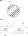
- Fig. 1 is a cross-sectional view showing a first example of the metal particle usable for the bonding material according to one embodiment of the present invention.
- a metal particle 1 shown in Fig. 1 includes a base particle 2 and a metal layer 3 disposed on a surface of the base particle 2.
- the metal layer 3 covers the surface of the base particle 2.
- the metal particle 1 is a covered particle in which the surface of the base particle 2 is covered with the metal layer 3.
- the metal layer 3 includes a second metal layer 3A and a solder layer 3B (first metal layer).
- the metal particle 1 includes the second metal layer 3A between the base particle 2 and the solder layer 3B. Accordingly, the metal particle 1 includes the base particle 2, the second metal layer 3A disposed on the surface of the base particle 2, and the solder layer 3B disposed on an outer surface of the second metal layer 3A.
- the metal layer 3 may have a multilayer structure of two or more layers, or may have a multilayer structure.
- Fig. 2 is a cross-sectional view showing a second example of the metal particle usable for the bonding material according to one embodiment of the present invention.
- the metal layer 3 of the metal particle 1 in Fig. 1 has a two-layer structure.
- a metal particle 1A shown in Fig. 2 has a solder layer 4 as a single-layer metal layer.
- the metal particle 1A includes the base particle 2 and the solder layer 4 disposed on the surface of the base particle 2.
- the base particle examples include resin particles, inorganic particles excluding metal-containing particles, organic-inorganic hybrid particles, and metal-containing particles.
- the base particle is preferably a base particle excluding a metal-containing particle, and is preferably a resin particle, an inorganic particle excluding a metal-containing particle, or an organic-inorganic hybrid particle.
- the base particle may be a core-shell particle including a core and a shell disposed on a surface of the core.
- the core may be an organic core
- the shell may be an inorganic shell.
- the material of the resin particle include polyolefin resins such as polyethylene, polypropylene, polystyrene, polyvinyl chloride, polyvinylidene chloride, polyisobutylene, and polybutadiene; acrylic resins such as polymethyl methacrylate and polymethyl acrylate; polycarbonate, polyamide, phenol formaldehyde resin, melamine formaldehyde resin, benzoguanamine formaldehyde resin, urea formaldehyde resin, phenol resin, melamine resin, benzoguanamine resin, urea resin, epoxy resin, unsaturated polyester resin, saturated polyester resin, polyethylene terephthalate, polysulfone, polyphenylene oxide, polyacetal, polyimide, polyamideimide, polyether ether ketone, polyether sulfone, divinylbenzene polymer, and divinylbenzene-based copolymer.
- polyolefin resins such as polyethylene, polypropylene, polys
- the divinylbenzene-based copolymer examples include divinylbenzene-styrene copolymer and divinylbenzene-(meth)acrylate copolymer. Since the hardness of the resin particle can be easily controlled within a preferable range, the material of the resin particle is preferably a polymer obtained by polymerizing one or more polymerizable monomers having an ethylenically unsaturated group.
- examples of the polymerizable monomer having the ethylenically unsaturated group include non-crosslinkable monomers and crosslinkable monomers.
- non-crosslinkable monomers examples include styrene-based monomers such as styrene and ⁇ -methylstyrene; carboxyl group-containing monomers such as (meth)acrylic acid, maleic acid, and maleic anhydride; alkyl (meth)acrylate compounds such as methyl (meth)acrylate, ethyl (meth)acrylate, propyl (meth)acrylate, butyl (meth)acrylate, 2-ethyl hexyl (meth)acrylate, lauryl (meth)acrylate, cetyl (meth)acrylate, stearyl (meth)acrylate, and isobornyl (meth)acrylate; oxygen atom-containing (meth)acrylate compounds such as 2-hydroxyethyl (meth)acrylate, glycerol (meth)acrylate, polyoxyethylene (meth)acrylate, and glycidyl (meth)acrylate; nitrile-containing monomers such as
- crosslinkable monomers examples include polyfunctional (meth)acrylate compounds such as tetramethylolmethane tetra(meth)acrylate, tetramethylolmethane tri(meth)acrylate, tetramethylolmethane di(meth)acrylate, trimethylolpropane tri(meth)acrylate, dipentaerythritol hexa(meth)acrylate, dipentaerythritol penta(meth)acrylate, glycerol tri(meth)acrylate, glycerol di(meth)acrylate, (poly)ethylene glycol di(meth)acrylate, (poly)propylene glycol di(meth)acrylate, (poly)tetramethylene glycol di(meth)acrylate, and 1,4-butanediol di(meth)acrylate; and silane-containing monomers such as triallyl (iso)cyanurate, triallyl trimellitate, diviners
- (meth)acrylate refers to an acrylate and a methacrylate.
- (meth)acrylic refers to an acrylic and a methacrylic.
- (meth)acryloyl refers to an acryloyl and a methacryloyl.
- the resin particle can be obtained by polymerizing the polymerizable monomer having an ethylenically unsaturated group by a known method.
- this method include a method of suspension polymerization in the presence of a radical polymerization initiator, and a method of swelling and polymerizing monomers together with a radical polymerization initiator using non-crosslinked seed particles.
- the base particle is an inorganic particle excluding a metal-containing particle or an organic-inorganic hybrid particle
- examples of the inorganic substance for forming the base particle include silica, alumina, barium titanate, zirconia, and carbon black. It is preferable that the inorganic substance is not a metal.
- the particles formed of the silica are not particularly limited, and examples thereof include particles obtained by hydrolyzing a silicon compound having two or more hydrolyzable alkoxysilyl groups to form crosslinked polymer particles and then performing firing as necessary.
- the organic-inorganic hybrid particles include organic-inorganic hybrid particles formed of crosslinked alkoxysilyl polymer and an acrylic resin.
- the organic-inorganic hybrid particle is preferably a core-shell type organic-inorganic hybrid particle having a core and a shell disposed on the surface of the core.
- the core is preferably an organic core.
- the shell is preferably an inorganic shell.
- the base particle is preferably an organic-inorganic hybrid particle having an organic core and an inorganic shell disposed on the surface of the organic core.
- Examples of the material of the organic core include the material of the resin particle described above.
- the material of the inorganic shell examples include the inorganic substances exemplified as the material of the base particle described above.
- the material of the inorganic shell is preferably silica. It is preferable that the inorganic shell is formed by forming metal alkoxide into a shell-like material on the surface of the core by a sol-gel method and then firing the shell-like material.
- the metal alkoxide is preferably a silane alkoxide. It is preferable that the inorganic shell is formed of a silane alkoxide.
- the base particle is a metal-containing particle
- the metal as the material of the metal-containing particle include silver, copper, nickel, silicon, gold and titanium.
- the particle diameter of the base particle is not particularly limited.
- the particle diameter of the base particle can be appropriately selected according to a gap of a target air cavity.
- the particle diameter of the base particle may be, for example, 80 ⁇ m or more and 900 ⁇ m or less.
- the particle diameter of the base particle indicates the diameter when the base particle has a spherical shape, and indicates an equivalent sphere diameter when the base particle does not have a spherical shape.
- the particle diameter of the base particle is preferably a number average particle diameter.
- the particle diameter of the base particle is determined using a particle size distribution measuring device or the like.
- the particle diameter of the base particle is preferably determined by observing arbitrary 50 base particles with an electron microscope or an optical microscope and calculating an average value. In the observation with the electron microscope or the optical microscope, the particle diameter of the base particle per particle is determined as a particle diameter corresponding to an equivalent circle diameter. In the observation with the electron microscope or the optical microscope, the average particle diameter obtained from the equivalent circle diameters of arbitrary 50 base particles is substantially equal to the average particle diameter corresponding to an equivalent sphere diameter. In the laser diffraction type particle size distribution measurement, the particle diameter of the base particle per particle is determined as a particle diameter corresponding to an equivalent sphere diameter.
- the metal particle preferably includes a base particle and a metal layer disposed on a surface of the base particle.
- the metal layer may have a single layer structure or a multilayer structure of two or more layers.
- the metal particle preferably includes a base particle, a second metal layer disposed on a surface of the base particle, and a solder layer (first metal layer) disposed on a surface of the second metal layer.
- the metal particle preferably has solder on an outer surface portion of the metal layer.
- the metal layer includes a metal.
- the metal constituting the metal layer is not particularly limited. Examples of the metal include gold, silver, copper, platinum, palladium, zinc, lead, aluminum, cobalt, indium, nickel, chromium, titanium, antimony, bismuth, germanium, cadmium, and alloys of these.
- As the metal tin-doped indium oxide (ITO) and solder may be used. One kind of the metal may be used alone, and two or more kinds thereof may be used in combination. From the viewpoint of controlling the gap of the air cavity with higher accuracy and further increasing the bonding strength between the substrates, the metal contained in the metal layer as the outermost layer is preferably solder.
- the melting point of the base particle is preferably higher than the melting point of the metal layer.
- the melting point of the base particle is preferably more than 160°C, more preferably more than 300°C, still more preferably more than 400°C, particularly preferably more than 450°C.
- the melting point of the base particle may be less than 400°C.
- the melting point of the base particle may be 160°C or less.
- the softening point of the base particle is preferably 260°C or more. The softening point of the base particle may be less than 260°C.
- the metal particle may have a single layer solder layer.
- the metal particle may have a plurality of metal layers (a second metal layer and a solder layer (first metal layer)). That is, in the metal particle, two or more metal layers may be stacked. When two or more metal layers are stacked, the metal particle preferably has solder on the outer surface portion of the metal layer.
- the solder is preferably a metal (low melting point metal) having a melting point of 450°C or less.
- the solder layer is preferably a metal layer (low melting point metal layer) having a melting point of 450°C or less.
- the low melting point metal layer is a layer containing a low melting point metal.
- the solder in the metal particle is preferably a metal (low melting point metal) having a melting point of 450°C or less.
- the low melting point metal indicates a metal having a melting point of 450°C or less.
- the melting point of the low melting point metal is preferably 300°C or less, more preferably 220°C or less.
- the melting point of the low melting point metal can be determined by differential scanning calorimetry (DSC).
- DSC differential scanning calorimetry
- Examples of a differential scanning calorimetry (DSC) device include "EXSTAR DSC 7020" manufactured by Seiko Instruments Inc.
- the solder in the metal particle preferably contains tin.
- the content of tin in 100% by weight of metal contained in the solder in the metal particle is preferably 30% by weight or more, more preferably 40% by weight or more, still more preferably 70% by weight or more, particularly preferably 90% by weight or more.
- the bonding strength between the substrates can be further enhanced.
- the content of tin can be measured by using a highfrequency induction coupling plasma emission spectrometry apparatus ("ICP-AES” manufactured by Horiba, Ltd.), a fluorescence X-ray analyzing apparatus (“EDX-800HS” manufactured by Shimadzu Corporation), or the like.
- ICP-AES highfrequency induction coupling plasma emission spectrometry apparatus
- EDX-800HS fluorescence X-ray analyzing apparatus
- the bonding material containing metal particles having the solder on the outer surface portion of the metal layer is used for bonding the metal portions formed on the two substrates to each other, the solder can be melted to be joined to the metal portion.
- the bonding strength between the substrates can be further enhanced, and a contact area between the metal particles and the metal portion can be sufficiently increased.
- the low melting point metal constituting the solder layer and the solder in the metal particle is not particularly limited.
- the low melting point metal is preferably tin or an alloy containing tin.
- the alloy include tin-silver alloy, tin-copper alloy, tin-silver-copper alloy, tin-bismuth alloy, tin-zinc alloy, and tin-indium alloy.
- the low melting point metal is preferably tin, tin-silver alloy, tin-silver-copper alloy, tin-bismuth alloy, or tin-indium alloy because of being excellent in wettability to the metal portion.
- the material for forming the solder layer and the solder in the metal particle is preferably a filler material having a liquidus line of 450°C or lower in accordance with JIS Z3001: Welding Terms.
- Examples of the composition of the solder include metallic compositions including zinc, gold, silver, lead, copper, tin, bismuth and indium.
- the solder in the metal particle may contain a metal such as nickel, copper, antimony, aluminum, zinc, iron, gold, titanium, phosphorus, germanium, tellurium, cobalt, bismuth, manganese, chromium, molybdenum, or palladium.
- the solder in the metal particle preferably contains nickel, copper, or antimony.
- the content of these metals for increasing the bonding strength is preferably 0.001% by weight or more and preferably 1% by weight or less in 100% by weight of the solder in the metal particle.
- the metal particle preferably includes a base particle, a second metal layer disposed on a surface of the base particle, and a solder layer disposed on a surface of the second metal layer.
- the melting point of the second metal layer is preferably higher than the melting point of the solder layer.
- the melting point of the second metal layer is preferably more than 220°C, more preferably more than 300°C, still more preferably more than 400°C, even more preferably more than 450°C, particularly preferably more than 500°C, most preferably more than 600°C. Since the solder layer has a low melting point, it is preferable that the solder layer is melted when an air cavity is formed. The second metal layer is preferably not melted when the air cavity is formed.
- the metal particle is used by melting the solder, it is preferable that the metal particle is used by melting the solder layer, and it is preferable that the metal particle is used by melting the solder layer without melting the second metal layer. Since the melting point of the second metal layer is higher than the melting point of the solder layer, only the solder layer can be melted without melting the second metal layer when the air cavity is formed.
- An absolute value of a difference between the melting point of the solder layer and the melting point of the second metal layer is more than 0°C, preferably 5°C or more, more preferably 10°C or more, still more preferably 30°C or more, particularly preferably 50°C or more, most preferably 100°C or more.
- the second metal layer includes a metal.
- the metal constituting the second metal layer is not particularly limited. Examples of the metal include gold, silver, copper, platinum, palladium, zinc, lead, aluminum, cobalt, indium, nickel, chromium, titanium, antimony, bismuth, germanium, cadmium, and alloys of these.
- the metal tin-doped indium oxide (ITO) may be used. One kind of the metal may be used alone, and two or more kinds thereof may be used in combination.
- the second metal layer is preferably a nickel layer, a palladium layer, a copper layer, or a gold layer, more preferably a nickel layer, a gold layer, or a copper layer, and still more preferably a copper layer.
- the metal particle preferably has a nickel layer, a palladium layer, a copper layer, or a gold layer, more preferably a nickel layer, a gold layer, or a copper layer, and still more preferably a copper layer.
- the thickness of the metal layer is preferably 3.5 ⁇ m or more, more preferably 8 ⁇ m or more, and preferably 80 ⁇ m or less, more preferably 65 ⁇ m or less, still more preferably 50 ⁇ m or less.
- the thickness of the metal layer is equal to or more than the above lower limit and equal to or less than the above upper limit, the bonding strength between the substrates can be further enhanced.
- the thickness of the second metal layer is preferably 0.5 ⁇ m or more, more preferably 3 ⁇ m or more, and preferably 30 ⁇ m or less, more preferably 25 ⁇ m or less, still more preferably 20 ⁇ m or less.
- the bonding strength between the substrates can be further enhanced.
- the thickness of the solder layer is preferably 3 ⁇ m or more, more preferably 5 ⁇ m or more, and preferably 50 ⁇ m or less, more preferably 40 ⁇ m or less, still more preferably 30 ⁇ m or less.
- the thickness of the solder layer is equal to or more than the above lower limit and equal to or less than the above upper limit, the bonding strength between the substrates can be further enhanced.
- the thickness of the metal layer, the thickness of the second metal layer, and the thickness of the solder layer can be measured, for example, by observing a cross section of the metal particle using a transmission electron microscope (TEM).
- TEM transmission electron microscope
- a method of forming the metal layer on the surface of the base particle is not particularly limited.
- Examples of the method of forming the metal layer include a method by electroless plating, a method by electroplating, a method by physical collision, a method by mechanochemical reaction, a method by physical vapor deposition or physical adsorption, and a method of coating paste containing a metal powder or paste containing a metal powder and a binder on the surface of the base particle.
- the method of forming the metal layer is preferably the method by electroless plating, electroplating, or physical collision.
- Examples of the method by physical vapor deposition include methods of vacuum deposition, ion plating, ion sputtering and the like. In the method by physical collision, for example, Theta Composer (manufacture by TOKUJU Co., LTD) or the like is used.
- the antenna device includes a first substrate having a first metal portion on its surface, a second substrate having a second metal portion on its surface, and a bonding material portion that bonds the first substrate and the second substrate.
- the material of the bonding material portion is the above-described bonding material.
- the first metal portion and the second metal portion are bonded by the bonding material portion.
- an air cavity is formed by the first substrate, the second substrate, and the bonding material portion.
- the first substrate is preferably a glass epoxy substrate or a ceramic substrate.
- the second substrate is preferably a glass epoxy substrate, a ceramic substrate, or a silicon substrate.
- the substrate may be a high frequency substrate, a substrate constituting an antenna, or the like.
- the first metal portion is preferably formed of copper or formed by nickel/gold plating.
- the second metal portion is preferably formed of copper or formed by nickel/gold plating.
- the first metal portion and the second metal portion may be formed of copper or formed by nickel/gold plating.
- Fig. 3 is a cross-sectional view showing an example of an antenna device using the bonding material according to the present invention.
- An antenna device 11 shown in Fig. 3 includes a first substrate 12, a second substrate 13, and a bonding material portion that bonds the first substrate 12 and the second substrate 13.
- the material of the bonding material portion is the bonding material described above.
- the material of the bonding material portion is the metal particle 1.
- the bonding material portion is preferably formed of the metal particles.
- the first substrate 12 has a plurality of first metal portions 12a on its surface (upper surface).
- the second substrate 13 has a plurality of second metal portions 13a on its surface (lower surface).
- the first metal portion 12a and the second metal portion 13a are bonded by one or the plurality of metal particles 1 (bonding material portion).
- an air cavity 14 is formed by the first substrate 12, the second substrate 13, and the metal particle 1 (bonding material portion).
- An interval (gap) between the first substrate 12 and the second substrate 13 is kept constant by the metal particle 1 (bonding material portion).
- a gap of the air cavity 14 is controlled by the metal particle 1 (bonding material portion).
- the gap in the antenna device may be set according to a frequency band targeted by the antenna device.
- a method of producing the antenna device is not particularly limited.
- An example of the method of producing the antenna device includes a method in which the bonding material described above is disposed between the first metal portion and the second metal portion to obtain a laminate, and then the laminate is heated and pressurized.
- the pressurization pressure is about 9.8 ⁇ 10 4 Pa to 4.9 ⁇ 10 6 Pa.
- the heating temperature is about 120°C to 250°C. From the viewpoint of controlling the gap of the air cavity with higher accuracy, it is preferable not to apply pressure at the time of manufacturing the antenna device. Since the molten solder layer of the metal particle is not excessively wetted and spread on the first metal portion and the second metal portion by not applying pressure at the time of manufacturing the antenna device, the gap of the air cavity can be controlled with higher accuracy.
- Fig. 4 is an enlarged cross-sectional view showing a bonding portion between the metal particle and the metal portion in the antenna device shown in Fig. 3 .
- the solder layer 3B of the metal particle 1 is melted by heating the laminate, and then a melted solder layer portion 3Ba sufficiently comes into contact with the first metal portion 12a and the second metal portion 13a.
- the metal particle 1 in which the outermost layer is a solder layer a contact area between the metal particle 1 and the first and second metal portions 12a and 13a can be increased as compared with the case of using the metal particle in which the outermost layer is a metal such as nickel, gold, or copper, and the gap of the air cavity can be controlled with higher accuracy.
- the metal particle 1 that is not the solder particle formed of solder by using the metal particle 1 that is not the solder particle formed of solder, excessive wetting and spreading of the solder due to heating can be suppressed even in the case of repeated heating, and the gap of the air cavity can be controlled with higher accuracy, as compared with the case of using a solder particle in which both the center portion and the outer surface portion of the metal layer are formed of solder.
- Divinylbenzene (50 parts by weight) and tetramethylolmethane tetraacrylate (50 parts by weight) were copolymerized to prepare base particles (average particle diameter 240 ⁇ m, CV value 1.85%) as resin particles.
- the obtained base particles were subjected to electroless nickel plating to form an underlying nickel plating layer having a thickness of 0.3 ⁇ m on the surface of the base particles.
- the base particle on which the underlying nickel plating layer was formed was subjected to electrolytic copper plating to form a copper layer having a thickness of 10 ⁇ m.
- electrolytic plating was performed to form a solder layer containing tin having a thickness of 25 ⁇ m.
- Base particles (average particle size 260 ⁇ m, CV value 1.92%) as resin particles were prepared in the same manner as in the metal particles 1.
- the obtained base particles were subjected to electroless nickel plating to form an underlying nickel plating layer having a thickness of 0.3 ⁇ m on the surface of the base particles.
- the base particle on which the underlying nickel plating layer was formed was subjected to electrolytic copper plating to form a copper layer having a thickness of 5 ⁇ m.
- electrolytic plating was performed to form a solder layer containing tin having a thickness of 20 ⁇ m.
- Base particles (average particle size 210 ⁇ m, CV value 1.68%) as resin particles were prepared in the same manner as in the metal particles 1.
- the obtained base particles were subjected to electroless nickel plating to form an underlying nickel plating layer having a thickness of 0.3 ⁇ m on the surface of the base particles.
- the base particle on which the underlying nickel plating layer was formed was subjected to electrolytic copper plating to form a copper layer having a thickness of 10 ⁇ m.
- electrolytic plating was performed to form a solder layer containing tin having a thickness of 40 ⁇ m.
- the average particle diameter of the metal particles was measured by the method described above using a digital microscope ("VHX-5000" manufactured by KEYENCE CORPORATION).
- the obtained metal particles 1 themselves were used as a bonding material without using a bonding component other than the metal particles 1.
- first substrate a glass epoxy substrate having 20 metal portions (first metal portions) formed of copper was prepared.
- second substrate a glass epoxy substrate having 20 metal portions (second metal portions) formed of copper was prepared.
- the metal portion is a metal portion for forming an antenna circuit.
- a flux (“WS-9160-M7” manufactured by Cookson Electronics) was applied onto the surface of the first metal portion of the first substrate. Subsequently, the metal particles 1 were arranged on the surface of the applied flux, and reflow treatment (heating temperature 250°C and heating time 30 seconds) was performed to bond the metal particles 1 to the first metal portion.
- a solder paste (“M705-GRN360-K2-V” manufactured by Senju Metal Industry Co., Ltd.) was applied onto the surface of the second metal portion of the second substrate.
- a bonding structure of the first substrate and the metal particles 1 and the second substrate to which the solder paste was applied were arranged so that the first metal portion and the second metal portion faced each other, and reflow treatment (heating temperature 250°C and heating time 30 seconds) was performed.
- reflow treatment heating temperature 250°C and heating time 30 seconds
- An antenna device B was prepared in the same manner as in the method of preparing the antenna device A except that a glass epoxy substrate having 20 metal portions (second metal portions) formed by nickel/gold plating was used as the second substrate.
- An antenna device C was prepared in the same manner as in the method of preparing the antenna device A except that a glass epoxy substrate having 20 metal portions (second metal portions) formed by nickel/gold plating was used as the first and second substrates.
- the antenna devices A, B, and C were prepared in the same manner as in Example 1 except that the metal particles 2 were used as a bonding material instead of the metal particles 1.
- the antenna devices A, B, and C were prepared in the same manner as in Example 1 except that the metal particles 3 were used as a bonding material instead of the metal particles 1.
- the antenna devices A, B, and C were prepared in the same manner as in Example 1 except that the metal particles X1 were used as a bonding material instead of the metal particles 1.
- the obtained metal particles (bonding material) were provided.
- a first substrate glass epoxy substrate
- a second substrate glass epoxy substrate
- the rate of change in gap between the substrates was calculated by the method described above.
- the obtained metal particles (bonding material) were provided.
- a first substrate glass epoxy substrate
- a second substrate glass epoxy substrate
- the rate of change in gap between the substrates was calculated by the method described above.
- the obtained metal particles (bonding material) were provided.
- a first substrate (glass epoxy substrate) having a first metal portion formed by nickel/gold plating on its surface was provided.
- a second substrate (glass epoxy substrate) having a second metal portion formed by nickel/gold plating on its surface was provided.
- the rate of change in gap between the substrates was calculated by the method described above.
- the obtained metal particles (bonding material) were provided.
- a first substrate glass epoxy substrate
- a second substrate glass epoxy substrate
- the ratio (the gap after heating/the average particle diameter of the metal particles) was calculated by the method described above.
- the obtained metal particles (bonding material) were provided.
- a first substrate glass epoxy substrate
- a second substrate glass epoxy substrate
- the ratio (the gap after heating/the average particle diameter of the metal particles) was calculated by the method described above.
- the obtained metal particles (bonding material) were provided.
- a first substrate (glass epoxy substrate) having a first metal portion formed by nickel/gold plating on its surface was provided.
- a second substrate (glass epoxy substrate) having a second metal portion formed by nickel/gold plating on its surface was provided.
- the ratio was calculated by the method described above.
- the obtained metal particles (bonding material) were provided.
- a first substrate glass epoxy substrate
- a second substrate glass epoxy substrate
- the rate of change in bonding strength between the substrates was calculated by the method described above.
- the obtained metal particles (bonding material) were provided.
- a first substrate (glass epoxy substrate) having a first metal portion formed by nickel/gold plating on its surface was provided.
- a second substrate (glass epoxy substrate) having a second metal portion formed by nickel/gold plating on its surface was provided.
- the rate of change in bonding strength between the substrates was calculated by the method described above.
- the thickness of the air cavity of each of the five antenna devices A obtained was measured using a stereoscopic microscope ("SMZ-10" manufactured by Nikon Corporation), and an average thickness of the air cavity in each of the five antenna devices A was calculated. From a difference between a maximum value of the average thickness and a minimum value of the average thickness, gap controllability was determined according to the following criteria.
- the obtained antenna devices B and C were also evaluated in the same manner.
- reflow treatment was performed four times under the reflow conditions specified in JEDEC J-STD-020.
- the antenna device A after reflow treatment was evaluated in the same manner as in (4) Gap controllability.
- the gap controllability after reflow treatment was determined according to the following criteria.
- the obtained antenna devices B and C were also evaluated in the same manner.
- the antenna device A After the evaluation of (5) Gap controllability after reflow treatment.
- the communication quality of the antenna was judged according to the following criteria.
- the obtained antenna devices B and C were also evaluated in the same manner.
Landscapes
- Chemical & Material Sciences (AREA)
- Organic Chemistry (AREA)
- Engineering & Computer Science (AREA)
- Chemical Kinetics & Catalysis (AREA)
- Metallurgy (AREA)
- Materials Engineering (AREA)
- Mechanical Engineering (AREA)
- General Chemical & Material Sciences (AREA)
- Electrochemistry (AREA)
- Microelectronics & Electronic Packaging (AREA)
- Manufacturing & Machinery (AREA)
- Inorganic Chemistry (AREA)
- Health & Medical Sciences (AREA)
- Medicinal Chemistry (AREA)
- Polymers & Plastics (AREA)
- Adhesives Or Adhesive Processes (AREA)
- Combinations Of Printed Boards (AREA)
- Laminated Bodies (AREA)
Abstract
Description
- The present invention relates to a bonding material for bonding two substrates. The present invention also relates to an antenna device using the bonding material.
- Various bonding materials are used for bonding two adherends. In order to make a thickness of a bonding layer formed by the bonding material uniform and to control an interval (gap) between the two adherends, a spacer such as a gap material may be blended in the bonding material.
- In recent years, with a rapid spread of smartphones, tablet terminals, and the like, a rapid increase in traffic has been a problem. For this reason, a fifth generation mobile communication system (5G) has been studied as a successor system of a communication system such as LTE (Long Term Evolution) or LTE-A (LTE-Advanced) by 3GPP (Third Generation Partnership Project) or a new wireless communication system.
- For example, in the fifth generation mobile communication system (5G), in order to achieve high-speed transmission using a wider band, it is considered to perform communication using a higher carrier frequency than LTE and LTE-A. However, when communication is performed at a high carrier frequency, there is a possibility that a conventional antenna device cannot sufficiently exhibit performance. The conventional antenna device is disclosed in, for example,
Patent Document 1 below. -
Patent Document 1 below discloses an antenna device including an antenna and a multilayer high frequency substrate. The antenna includes a feeding conductor on the back surface. The multilayer high frequency substrate is configured by stacking a plurality of strip lines including a land on its surface. The land is electrically connected to a strip conductor via a through hole. In the multilayer high frequency substrate, the lands of the strip lines to be stacked are joined with an anisotropic conductive bonding material. In the antenna device, the feeding conductor of the antenna and the land on the surface of the multilayer high frequency substrate are joined by an anisotropic conductive bonding material. - Patent Document 1:
JP 2015-185550 A - In antennas of a base station and a terminal for the fifth generation mobile communication system (5G), improvement in communication speed, improvement in communication quality, and the like are required. In order to achieve improvement in communication speed, improvement in communication quality, and the like, it has been studied to provide an air cavity (space) in an antenna. By providing the air cavity (space) in the antenna, a bandwidth can be improved, and electromagnetic wave noise can be reduced. As a result, the communication speed, the communication quality, and the like of the antenna can be improved.
- In the conventional antenna device, a high level of communication speed and a high level of communication quality are not required, and the air cavity (space) may not be provided in the antenna. The air cavity (space) is formed, for example, by keeping uniform and constant an interval (gap) between a high frequency substrate and a substrate constituting the antenna. In order to improve the communication speed, the communication quality, and the like of the antenna, it is required to control the interval (gap) of the air cavity (space) with high accuracy.
- When the antenna device is obtained by bonding two substrates using a bonding material so as to form an air cavity (space) in the antenna, the antenna device may be repeatedly heated. Since the antenna device is repeatedly heated, the interval (gap) of the air cavity (space) cannot be controlled with high accuracy, and it may be difficult to improve the communication speed, the communication quality, and the like of the antenna.
- An object of the present invention is to provide a bonding material capable of controlling the gap of the air cavity with high accuracy even when the bonding material is repeatedly heated. It is also an object of the present invention to provide an antenna device using the bonding material.
- According to a broad aspect of the present invention, there is provided a bonding material for bonding a first metal portion and a second metal portion to each other between a first substrate having the first metal portion on its surface and a second substrate having the second metal portion on its surface, in which a rate of change in gap between the substrates calculated by the following Evaluation Test 1a is 10% or less.
- The first substrate having the first metal portion on the surface, the second substrate having the second metal portion on the surface, and the bonding material are provided. The bonding material is disposed on the first metal portion of the first substrate, and the second substrate is disposed on a surface of the bonding material opposite to a side of the first substrate such that the first metal portion and the second metal portion face each other. Thereafter, the first substrate and the second substrate are bonded to each other by performing reflow treatment under reflow conditions defined in JEDEC J-STD-020 to obtain a laminate. The gap between the substrates of the obtained laminate is measured and taken as the gap before heating. Thereafter, the obtained laminate is subjected to reflow treatment four times under reflow conditions defined in JEDEC J-STD-020, and the gap between the substrates of the laminate after reflow treatment is measured and taken as the gap after heating. From the gaps before and after heating, the rate of change in gap is calculated by the following Equation (1).

- In a specific aspect of the bonding material according to the present invention, the bonding material contains metal particles.
- According to a broad aspect of the present invention, there is provided a bonding material for bonding a first metal portion and a second metal portion to each other between a first substrate having the first metal portion on its surface and a second substrate having the second metal portion on its surface, in which the bonding material contains metal particles, and a ratio of a gap after heating calculated by the following Evaluation Test 1b to an average particle diameter of the metal particles is 0.70 or more and 0.97 or less.
- The first substrate having the first metal portion on the surface, the second substrate having the second metal portion on the surface, and the bonding material are provided. The bonding material is disposed on the first metal portion of the first substrate, and the second substrate is disposed on a surface of the bonding material opposite to a side of the first substrate such that the first metal portion and the second metal portion face each other. Thereafter, the first substrate and the second substrate are bonded to each other by performing reflow treatment under reflow conditions defined in JEDEC J-STD-020 to obtain a laminate. The obtained laminate is subjected to reflow treatment four times under reflow conditions defined in JEDEC J-STD-020, and the gap between the substrates of the laminate after reflow treatment is measured and taken as the gap after heating.
- In a specific aspect of the bonding material according to the present invention, the metal particle includes a base particle and a metal layer disposed on a surface of the base particle.
- In a specific aspect of the bonding material according to the present invention, the metal layer includes a second metal layer disposed on a surface of the base particle and a first metal layer disposed on a surface of the second metal layer, and the first metal layer is a solder layer.
- In a specific aspect of the bonding material according to the present invention, a rate of change in bonding strength between the substrates calculated by the following
Evaluation Test 2 is 10% or less. - The first substrate having the first metal portion on the surface, the second substrate having the second metal portion on the surface, and the bonding material are provided. The bonding material is disposed on the first metal portion of the first substrate, and the second substrate is disposed on a surface of the bonding material opposite to a side of the first substrate such that the first metal portion and the second metal portion face each other. Thereafter, the first substrate and the second substrate are bonded to each other by performing reflow treatment under reflow conditions defined in JEDEC J-STD-020 to obtain a laminate. Using the obtained laminate, the bonding strength between the substrates is measured under conditions conforming to MIL STD-883G, and taken as the bonding strength before heating. Thereafter, the obtained laminate is subjected to reflow treatment four times under reflow conditions defined in JEDEC J-STD-020, and the bonding strength between the substrates is measured using the laminate after reflow treatment under conditions conforming to MIL STD-883G, and taken as the bonding strength after heating. From the bonding strength before and after heating, the rate of change in bonding strength is calculated by the following Equation (2).

- In a specific aspect of the bonding material according to the present invention, the first substrate is a glass epoxy substrate or a ceramic substrate, and the second substrate is a glass epoxy substrate, a ceramic substrate, or a silicon substrate.
- In a specific aspect of the bonding material according to the present invention, the first metal portion is formed of copper or formed by nickel/gold plating, and the second metal portion is formed of copper or formed by nickel/gold plating.
- According to a broad aspect of the present invention, there is provided an antenna device including: a first substrate having a first metal portion on its surface; a second substrate having a second metal portion on its surface; and a bonding material portion that bonds the first substrate and the second substrate to each other, in which a material of the bonding material portion is the above-described bonding material, the first metal portion and the second metal portion are bonded to each other by the bonding material portion, and an air cavity is formed by the first substrate, the second substrate, and the bonding material portion.
- In a specific aspect of the antenna device according to the present invention, the first substrate is a glass epoxy substrate or a ceramic substrate, and the second substrate is a glass epoxy substrate, a ceramic substrate, or a silicon substrate.
- In a specific aspect of the antenna device according to the present invention, the first metal portion is formed of copper or formed by nickel/gold plating, and the second metal portion is formed of copper or formed by nickel/gold plating.
- The bonding material according to the present invention is a bonding material for bonding a first metal portion and a second metal portion to each other between a first substrate having the first metal portion on its surface and a second substrate having the second metal portion on its surface. In the bonding material according to the present invention, the rate of change in gap between the substrates calculated by the Evaluation Test 1a is 10% or less. Since the bonding material according to the present invention has the above-described configuration, the gap of the air cavity can be controlled with high accuracy even when the bonding material is repeatedly heated.
- The bonding material according to the present invention is a bonding material for bonding a first metal portion and a second metal portion to each other between a first substrate having the first metal portion on its surface and a second substrate having the second metal portion on its surface. The bonding material according to the present invention contains metal particles. In the bonding material according to the present invention, the ratio of the gap after heating calculated by the Evaluation Test 1b to the average particle diameter of the metal particles is 0.70 or more and 0.97 or less. Since the bonding material according to the present invention has the above-described configuration, the gap of the air cavity can be controlled with high accuracy even when the bonding material is repeatedly heated.
-
- [
Fig. 1] Fig. 1 is a cross-sectional view showing a first example of a metal particle usable for a bonding material according to one embodiment of the present invention. - [
Fig. 2] Fig. 2 is a cross-sectional view showing a second example of the metal particle usable for the bonding material according to one embodiment of the present invention. - [
Fig. 3] Fig. 3 is a cross-sectional view showing an example of an antenna device using the bonding material according to the present invention. - [
Fig. 4] Fig. 4 is an enlarged cross-sectional view showing a bonding portion between the metal particle and a metal portion in the antenna device shown inFig. 3 . - Hereinafter, the details of the present invention will be described.
- The bonding material according to the present invention is a bonding material for bonding a first metal portion and a second metal portion to each other between a first substrate having the first metal portion on its surface and a second substrate having the second metal portion on its surface. In the bonding material according to the present invention, the rate of change in gap between the substrates calculated by the following Evaluation Test 1a is 10% or less.
- The first substrate having the first metal portion on the surface, the second substrate having the second metal portion on the surface, and the bonding material are provided. The bonding material is disposed on the first metal portion of the first substrate, and the second substrate is disposed on a surface of the bonding material opposite to a side of the first substrate such that the first metal portion and the second metal portion face each other. Thereafter, the first substrate and the second substrate are bonded to each other by performing reflow treatment under reflow conditions defined in JEDEC J-STD-020 to obtain a laminate. The gap between the substrates of the obtained laminate is measured and taken as the gap before heating. That is, the gap before heating means the gap before the laminate is heated. Thereafter, the obtained laminate is subjected to reflow treatment four times under reflow conditions defined in JEDEC J-STD-020, and the gap between the substrates of the laminate after reflow treatment is measured and taken as the gap after heating. That is, the gap after heating means the gap after the laminate is heated four times. From the gaps before and after heating, the rate of change in gap is calculated by the following Equation (1).

- In the Evaluation Test 1a, it is preferable that the bonding material is disposed so that the gap before heating is 60 µm or more, and it is preferable that the bonding material is disposed so that the gap before heating is 850 µm or less.
- The bonding material according to the present invention is a bonding material for bonding a first metal portion and a second metal portion to each other between a first substrate having the first metal portion on its surface and a second substrate having the second metal portion on its surface. The bonding material according to the present invention contains metal particles. In the bonding material according to the present invention, the ratio of the gap after heating calculated by the following Evaluation Test 1b to the average particle diameter of the metal particles is 0.70 or more and 0.97 or less.
- The first substrate having the first metal portion on the surface, the second substrate having the second metal portion on the surface, and the bonding material are provided. The bonding material is disposed on the first metal portion of the first substrate, and the second substrate is disposed on a surface of the bonding material opposite to a side of the first substrate such that the first metal portion and the second metal portion face each other. Thereafter, the first substrate and the second substrate are bonded to each other by performing reflow treatment under reflow conditions defined in JEDEC J-STD-020 to obtain a laminate. The obtained laminate is subjected to reflow treatment four times under reflow conditions defined in JEDEC J-STD-020, and the gap between the substrates of the laminate after reflow treatment is measured and taken as the gap after heating.
- In the Evaluation Test 1b, it is preferable that the bonding material is disposed so that the gap between the substrates of the laminate (laminate before reflow treatment) is 60 µm or more, and it is preferable that the bonding material is disposed so that the gap is 850 µm or less.
- Since the bonding material according to the present invention has the above-described configuration, the gap of the air cavity can be controlled with high accuracy even when the bonding material is repeatedly heated.
- When the antenna device is obtained by bonding two substrates using a bonding material so as to form an air cavity (space) in the antenna, the antenna device may be repeatedly heated. In the antenna device obtained using a conventional bonding material, since the antenna device is repeatedly heated, the interval (gap) of the air cavity (space) cannot be controlled with high accuracy, and it may be difficult to improve the communication speed, the communication quality, and the like of the antenna.
- On the other hand, since the bonding material according to the present invention has the above-described configuration, the gap between the substrates can be controlled with high accuracy even when the bonding material is repeatedly heated, and the gap of the air cavity can be controlled with high accuracy. As a result, the communication speed, the communication quality, and the like of the antenna can be further improved.
- The bonding material according to the present invention is a bonding material for bonding a first metal portion and a second metal portion to each other between a first substrate having the first metal portion on its surface and a second substrate having the second metal portion on its surface. The bonding material according to the present invention is a bonding material for bonding two substrates. The bonding material according to the present invention is preferably a bonding material for bonding metal portions in two substrates to each other.
- In the bonding material according to the present invention, the rate of change in gap between the substrates calculated by the Evaluation Test 1a is 10% or less. The rate of change in gap between the substrates calculated by the Evaluation Test 1a is preferably 5% or less, more preferably 3% or less. When the rate of change in gap between the substrates calculated by the Evaluation Test 1a is equal to or less than the above upper limit, the gap of the air cavity can be controlled with high accuracy even in the case of repeated heating.
- In the bonding material according to the present invention, the ratio of the gap after heating calculated by the Evaluation Test 1b to the average particle diameter of the metal particles (the gap after heating calculated by the Evaluation Test 1b/the average particle diameter of the metal particles) is 0.70 or more and 0.97 or less. The ratio (the gap after heating calculated by the Evaluation Test 1b/the average particle diameter of the metal particles) is preferably 0.75 or more, more preferably 0.80 or more, and preferably 0.95 or less, more preferably 0.90 or less. When the ratio (the gap after heating calculated by the Evaluation Test 1b/the average particle diameter of the metal particles) is equal to or more than the above lower limit and equal to or less than the above upper limit, the gap of the air cavity can be controlled with high accuracy even in the case of repeated heating.
- In the bonding material, the rate of change in bonding strength between the substrates calculated by the following
Evaluation Test 2 is preferably 10% or less, more preferably 5% or less, still more preferably 3% or less When the rate of change in bonding strength between the substrates calculated by the followingEvaluation Test 2 is equal to or less than the above upper limit, the bonding strength between the substrates can be maintained even in the case of repeated heating, and the gap of the air cavity can be controlled with high accuracy. - The first substrate having the first metal portion on the surface, the second substrate having the second metal portion on the surface, and the bonding material are provided. The bonding material is disposed on the first metal portion of the first substrate, and the second substrate is disposed on a surface of the bonding material opposite to a side of the first substrate such that the first metal portion and the second metal portion face each other. Thereafter, the first substrate and the second substrate are bonded to each other by performing reflow treatment under reflow conditions defined in JEDEC J-STD-020 to obtain a laminate. Using the obtained laminate, the bonding strength between the substrates is measured under conditions conforming to MIL STD-883G, and taken as the bonding strength before heating. Thereafter, the obtained laminate is subjected to reflow treatment four times under reflow conditions defined in JEDEC J-STD-020, and the bonding strength between the substrates is measured using the laminate after reflow treatment under conditions conforming to MIL STD-883G, and taken as the bonding strength after heating. From the bonding strength before and after heating, the rate of change in bonding strength is calculated by the following Equation (2).

- In the
Evaluation Test 2, it is preferable that the bonding material is disposed so that the gap between the substrates of the laminate (laminate before reflow treatment) is 60 µm or more, and it is preferable that the bonding material is disposed so that the gap is 850 µm or less. - In the
Evaluation Test 2, the bonding strength before heating is preferably 1.5 kgf or more, and more preferably 2.0 kgf or more. When the bonding strength before heating is equal to or more than the above lower limit, the bonding strength between the substrates can be maintained even in the case of repeated heating, and the gap of the air cavity can be controlled with high accuracy. - In the Evaluation Test 1a, the Evaluation Test 1b, and the
Evaluation Test 2, the first substrate is preferably a glass epoxy substrate or a ceramic substrate. In the Evaluation Test 1a, the Evaluation Test 1b, and theEvaluation Test 2, the second substrate is preferably a glass epoxy substrate, a ceramic substrate, or a silicon substrate. - In the Evaluation Test 1a, the Evaluation Test 1b, and the
Evaluation Test 2, the first metal portion is preferably formed of copper or formed by nickel/gold plating. In the Evaluation Test 1a, the Evaluation Test 1b, and theEvaluation Test 2, the second metal portion is preferably formed of copper or formed by nickel/gold plating. - The Evaluation Test 1a, the Evaluation Test 1b, and the
Evaluation Test 2 are performed in order to calculate the rate of change in gap, the ratio (the gap after heating calculated by the Evaluation Test 1b/the average particle diameter of the metal particles), and the rate of change in bonding strength. When the bonding material is actually used, the bonding material may not be treated under the conditions defined in the Evaluation Test 1a, the Evaluation Test 1b, and theEvaluation Test 2. For example, when the bonding material is actually used, reflow treatment may not be performed under the reflow conditions defined in JEDEC J-STD-020. - The bonding material preferably contains metal particles from the viewpoint of controlling the gap of the air cavity with high accuracy even when the bonding material is repeatedly heated. The bonding material may or may not contain components other than the metal particles. From the viewpoint of controlling the gap of the air cavity with higher accuracy even when the bonding material is repeatedly heated, the bonding material preferably contains only the metal particles, and is preferably a particle group of a plurality of metal particles.
- The bonding material can bond two adherends, for example. The adherend is preferably a substrate, and more preferably a substrate having a metal portion on its surface. The bonding material is preferably used for bonding two substrates. The bonding material is preferably used for bonding the two metal portions to each other. Furthermore, the bonding material is preferably used for controlling the gap between the two substrates. The bonding material is preferably used for controlling the gap between the two substrates.
- The bonding material may be used for conductive connection or may not be used for conductive connection. The bonding material is preferably used for the antenna device. The bonding material is preferably used for forming an air cavity. The bonding material is preferably used for forming an air cavity in the antenna device. In the antenna device, the bonding material is preferably used for keeping uniform and constant an interval (gap) between a high frequency substrate and a substrate constituting the antenna. The bonding material forms an air cavity in the antenna device, and is preferably used for improving the communication speed, the communication quality, and the like of the antenna.
- The bonding material according to the present invention preferably contains metal particles. The metal particle means a particle containing a metal. The metal particle may have a constituent component other than metal. The metal particle preferably has, for example, a role of regulating an interval (gap) between two substrates. The metal particle is preferably not a solder particle formed only of solder. The metal particle preferably includes a base particle and a metal layer disposed on a surface of the base particle. The metal layer may have a single layer structure or a multilayer structure of two or more layers.
- The metal particle preferably has solder on an outer surface portion of the metal layer. The base particle is preferably not the solder particle formed only of solder. When the metal particle is a solder particle in which both a center portion and the outer surface portion of the metal layer are formed of solder, it may be difficult to control the gap of the air cavity because the solder wets and spreads due to heating in the case of repeated heating. When the metal particle is a metal particle having a base particle not formed of solder and a metal layer (solder layer) disposed on the surface of the base particle, excessive wetting and spreading of the solder due to heating can be suppressed even in the case of repeated heating, and therefore, the gap of the air cavity can be controlled with high accuracy. Accordingly, the metal particle is preferably not a solder particle formed of solder. In the metal particle, both the center portion and the outer surface portion of the metal layer are preferably not a solder particle formed of solder.
- The average particle diameter of the metal particles is not particularly limited. The average particle diameter of the metal particles can be appropriately selected according to a gap of a target air cavity. The average particle diameter of the metal particles may be, for example, 80 µm or more and 900 µm or less.
- The average particle diameter of the metal particles is preferably a number average particle diameter. The average particle diameter of the metal particles is determined by, for example, observing arbitrary 50 metal particles with an electron microscope or an optical microscope, and calculating an average value of the particle diameter of each metal particle or performing laser diffraction type particle size distribution measurement. In the observation with the electron microscope or the optical microscope, the particle diameter of the metal particle per particle is determined as a particle diameter corresponding to an equivalent circle diameter. In the observation with the electron microscope or the optical microscope, the average particle diameter obtained from the equivalent circle diameters of arbitrary 50 metal particles is substantially equal to the average particle diameter corresponding to an equivalent sphere diameter. In the laser diffraction type particle size distribution measurement, the particle diameter of the metal particle per particle is determined as a particle diameter corresponding to an equivalent sphere diameter.
- A variation coefficient (CV value) of the particle diameter of the metal particles is preferably 10% or less, more preferably 5% or less. When the variation coefficient of the particle diameter of the metal particle is equal to or less than the upper limit, the gap of the air cavity can be controlled with higher accuracy.
- The variation coefficient (CV value) can be measured as follows.

- ρ: standard deviation of particle diameter of metal particle
- Dn: average value of particle diameter of metal particle
- The shape of the metal particles is not particularly limited. The shape of the metal particle may be a spherical shape, a shape other than a spherical shape, or a shape such as a flat shape.
- Next, specific examples of the metal particles will be described with reference to the drawings.
-
Fig. 1 is a cross-sectional view showing a first example of the metal particle usable for the bonding material according to one embodiment of the present invention. - A
metal particle 1 shown inFig. 1 includes abase particle 2 and ametal layer 3 disposed on a surface of thebase particle 2. Themetal layer 3 covers the surface of thebase particle 2. Themetal particle 1 is a covered particle in which the surface of thebase particle 2 is covered with themetal layer 3. - The
metal layer 3 includes asecond metal layer 3A and asolder layer 3B (first metal layer). Themetal particle 1 includes thesecond metal layer 3A between thebase particle 2 and thesolder layer 3B. Accordingly, themetal particle 1 includes thebase particle 2, thesecond metal layer 3A disposed on the surface of thebase particle 2, and thesolder layer 3B disposed on an outer surface of thesecond metal layer 3A. As described above, themetal layer 3 may have a multilayer structure of two or more layers, or may have a multilayer structure. -
Fig. 2 is a cross-sectional view showing a second example of the metal particle usable for the bonding material according to one embodiment of the present invention. - The
metal layer 3 of themetal particle 1 inFig. 1 has a two-layer structure. A metal particle 1A shown inFig. 2 has asolder layer 4 as a single-layer metal layer. The metal particle 1A includes thebase particle 2 and thesolder layer 4 disposed on the surface of thebase particle 2. - Hereinafter, other details of the metal particle will be described.
- Examples of the base particle include resin particles, inorganic particles excluding metal-containing particles, organic-inorganic hybrid particles, and metal-containing particles. The base particle is preferably a base particle excluding a metal-containing particle, and is preferably a resin particle, an inorganic particle excluding a metal-containing particle, or an organic-inorganic hybrid particle. The base particle may be a core-shell particle including a core and a shell disposed on a surface of the core. The core may be an organic core, and the shell may be an inorganic shell.
- Various organic substances are suitably used as a material of the resin particle. Examples of the material of the resin particle include polyolefin resins such as polyethylene, polypropylene, polystyrene, polyvinyl chloride, polyvinylidene chloride, polyisobutylene, and polybutadiene; acrylic resins such as polymethyl methacrylate and polymethyl acrylate; polycarbonate, polyamide, phenol formaldehyde resin, melamine formaldehyde resin, benzoguanamine formaldehyde resin, urea formaldehyde resin, phenol resin, melamine resin, benzoguanamine resin, urea resin, epoxy resin, unsaturated polyester resin, saturated polyester resin, polyethylene terephthalate, polysulfone, polyphenylene oxide, polyacetal, polyimide, polyamideimide, polyether ether ketone, polyether sulfone, divinylbenzene polymer, and divinylbenzene-based copolymer. Examples of the divinylbenzene-based copolymer include divinylbenzene-styrene copolymer and divinylbenzene-(meth)acrylate copolymer. Since the hardness of the resin particle can be easily controlled within a preferable range, the material of the resin particle is preferably a polymer obtained by polymerizing one or more polymerizable monomers having an ethylenically unsaturated group.
- When the resin particle is obtained by polymerizing a polymerizable monomer having an ethylenically unsaturated group, examples of the polymerizable monomer having the ethylenically unsaturated group include non-crosslinkable monomers and crosslinkable monomers.
- Examples of the non-crosslinkable monomers include styrene-based monomers such as styrene and α-methylstyrene; carboxyl group-containing monomers such as (meth)acrylic acid, maleic acid, and maleic anhydride; alkyl (meth)acrylate compounds such as methyl (meth)acrylate, ethyl (meth)acrylate, propyl (meth)acrylate, butyl (meth)acrylate, 2-ethyl hexyl (meth)acrylate, lauryl (meth)acrylate, cetyl (meth)acrylate, stearyl (meth)acrylate, and isobornyl (meth)acrylate; oxygen atom-containing (meth)acrylate compounds such as 2-hydroxyethyl (meth)acrylate, glycerol (meth)acrylate, polyoxyethylene (meth)acrylate, and glycidyl (meth)acrylate; nitrile-containing monomers such as (meth)acrylonitrile; vinyl ether compounds such as methyl vinyl ether, ethyl vinyl ether, and propyl vinyl ether; acid vinyl ester compounds such as vinyl acetate, vinyl butyrate, vinyl laurate, and vinyl stearate; unsaturated hydrocarbons such as ethylene, propylene, isoprene, and butadiene; and halogen-containing monomers such as trifluoromethyl (meth)acrylate, pentafluoroethyl (meth)acrylate, vinyl chloride, vinyl fluoride, and chlorostyrene.
- Examples of the crosslinkable monomers include polyfunctional (meth)acrylate compounds such as tetramethylolmethane tetra(meth)acrylate, tetramethylolmethane tri(meth)acrylate, tetramethylolmethane di(meth)acrylate, trimethylolpropane tri(meth)acrylate, dipentaerythritol hexa(meth)acrylate, dipentaerythritol penta(meth)acrylate, glycerol tri(meth)acrylate, glycerol di(meth)acrylate, (poly)ethylene glycol di(meth)acrylate, (poly)propylene glycol di(meth)acrylate, (poly)tetramethylene glycol di(meth)acrylate, and 1,4-butanediol di(meth)acrylate; and silane-containing monomers such as triallyl (iso)cyanurate, triallyl trimellitate, divinylbenzene, diallyl phthalate, diallyl acrylamide, diallyl ether, and γ-(meth)acryloxy propyl trimethoxy silane, trimethoxy silyl styrene, and vinyltrimethoxysilane.
- The term "(meth)acrylate" refers to an acrylate and a methacrylate. The term "(meth)acrylic" refers to an acrylic and a methacrylic. The term "(meth)acryloyl" refers to an acryloyl and a methacryloyl.
- The resin particle can be obtained by polymerizing the polymerizable monomer having an ethylenically unsaturated group by a known method. Examples of this method include a method of suspension polymerization in the presence of a radical polymerization initiator, and a method of swelling and polymerizing monomers together with a radical polymerization initiator using non-crosslinked seed particles.
- When the base particle is an inorganic particle excluding a metal-containing particle or an organic-inorganic hybrid particle, examples of the inorganic substance for forming the base particle include silica, alumina, barium titanate, zirconia, and carbon black. It is preferable that the inorganic substance is not a metal. The particles formed of the silica are not particularly limited, and examples thereof include particles obtained by hydrolyzing a silicon compound having two or more hydrolyzable alkoxysilyl groups to form crosslinked polymer particles and then performing firing as necessary. Examples of the organic-inorganic hybrid particles include organic-inorganic hybrid particles formed of crosslinked alkoxysilyl polymer and an acrylic resin.
- The organic-inorganic hybrid particle is preferably a core-shell type organic-inorganic hybrid particle having a core and a shell disposed on the surface of the core. The core is preferably an organic core. The shell is preferably an inorganic shell. From the viewpoint of more effectively lowering connection resistance between the electrodes, the base particle is preferably an organic-inorganic hybrid particle having an organic core and an inorganic shell disposed on the surface of the organic core.
- Examples of the material of the organic core include the material of the resin particle described above.
- Examples of the material of the inorganic shell include the inorganic substances exemplified as the material of the base particle described above. The material of the inorganic shell is preferably silica. It is preferable that the inorganic shell is formed by forming metal alkoxide into a shell-like material on the surface of the core by a sol-gel method and then firing the shell-like material. The metal alkoxide is preferably a silane alkoxide. It is preferable that the inorganic shell is formed of a silane alkoxide.
- When the base particle is a metal-containing particle, examples of the metal as the material of the metal-containing particle include silver, copper, nickel, silicon, gold and titanium.
- The particle diameter of the base particle is not particularly limited. The particle diameter of the base particle can be appropriately selected according to a gap of a target air cavity. The particle diameter of the base particle may be, for example, 80 µm or more and 900 µm or less.
- The particle diameter of the base particle indicates the diameter when the base particle has a spherical shape, and indicates an equivalent sphere diameter when the base particle does not have a spherical shape.
- The particle diameter of the base particle is preferably a number average particle diameter. The particle diameter of the base particle is determined using a particle size distribution measuring device or the like. The particle diameter of the base particle is preferably determined by observing arbitrary 50 base particles with an electron microscope or an optical microscope and calculating an average value. In the observation with the electron microscope or the optical microscope, the particle diameter of the base particle per particle is determined as a particle diameter corresponding to an equivalent circle diameter. In the observation with the electron microscope or the optical microscope, the average particle diameter obtained from the equivalent circle diameters of arbitrary 50 base particles is substantially equal to the average particle diameter corresponding to an equivalent sphere diameter. In the laser diffraction type particle size distribution measurement, the particle diameter of the base particle per particle is determined as a particle diameter corresponding to an equivalent sphere diameter.
- The metal particle preferably includes a base particle and a metal layer disposed on a surface of the base particle. The metal layer may have a single layer structure or a multilayer structure of two or more layers. When the metal layer has a multilayer structure of two or more layers, the metal particle preferably includes a base particle, a second metal layer disposed on a surface of the base particle, and a solder layer (first metal layer) disposed on a surface of the second metal layer. The metal particle preferably has solder on an outer surface portion of the metal layer.
- The metal layer includes a metal. The metal constituting the metal layer is not particularly limited. Examples of the metal include gold, silver, copper, platinum, palladium, zinc, lead, aluminum, cobalt, indium, nickel, chromium, titanium, antimony, bismuth, germanium, cadmium, and alloys of these. As the metal, tin-doped indium oxide (ITO) and solder may be used. One kind of the metal may be used alone, and two or more kinds thereof may be used in combination. From the viewpoint of controlling the gap of the air cavity with higher accuracy and further increasing the bonding strength between the substrates, the metal contained in the metal layer as the outermost layer is preferably solder.
- The melting point of the base particle is preferably higher than the melting point of the metal layer. The melting point of the base particle is preferably more than 160°C, more preferably more than 300°C, still more preferably more than 400°C, particularly preferably more than 450°C. The melting point of the base particle may be less than 400°C. The melting point of the base particle may be 160°C or less. The softening point of the base particle is preferably 260°C or more. The softening point of the base particle may be less than 260°C.
- The metal particle may have a single layer solder layer. The metal particle may have a plurality of metal layers (a second metal layer and a solder layer (first metal layer)). That is, in the metal particle, two or more metal layers may be stacked. When two or more metal layers are stacked, the metal particle preferably has solder on the outer surface portion of the metal layer.
- The solder is preferably a metal (low melting point metal) having a melting point of 450°C or less. The solder layer is preferably a metal layer (low melting point metal layer) having a melting point of 450°C or less. The low melting point metal layer is a layer containing a low melting point metal. The solder in the metal particle is preferably a metal (low melting point metal) having a melting point of 450°C or less. The low melting point metal indicates a metal having a melting point of 450°C or less. The melting point of the low melting point metal is preferably 300°C or less, more preferably 220°C or less.
- The melting point of the low melting point metal can be determined by differential scanning calorimetry (DSC). Examples of a differential scanning calorimetry (DSC) device include "EXSTAR DSC 7020" manufactured by Seiko Instruments Inc.
- The solder in the metal particle preferably contains tin. The content of tin in 100% by weight of metal contained in the solder in the metal particle is preferably 30% by weight or more, more preferably 40% by weight or more, still more preferably 70% by weight or more, particularly preferably 90% by weight or more. When the content of tin contained in the solder in the metal particle is equal to or more than the above lower limit, the bonding strength between the substrates can be further enhanced.
- The content of tin can be measured by using a highfrequency induction coupling plasma emission spectrometry apparatus ("ICP-AES" manufactured by Horiba, Ltd.), a fluorescence X-ray analyzing apparatus ("EDX-800HS" manufactured by Shimadzu Corporation), or the like.
- When the bonding material containing metal particles having the solder on the outer surface portion of the metal layer is used for bonding the metal portions formed on the two substrates to each other, the solder can be melted to be joined to the metal portion. For example, since the solder and the metal portion are easily brought into surface contact rather than point contact, the bonding strength between the substrates can be further enhanced, and a contact area between the metal particles and the metal portion can be sufficiently increased.
- The low melting point metal constituting the solder layer and the solder in the metal particle is not particularly limited. The low melting point metal is preferably tin or an alloy containing tin. Examples of the alloy include tin-silver alloy, tin-copper alloy, tin-silver-copper alloy, tin-bismuth alloy, tin-zinc alloy, and tin-indium alloy. Among these, the low melting point metal is preferably tin, tin-silver alloy, tin-silver-copper alloy, tin-bismuth alloy, or tin-indium alloy because of being excellent in wettability to the metal portion.
- The material for forming the solder layer and the solder in the metal particle is preferably a filler material having a liquidus line of 450°C or lower in accordance with JIS Z3001: Welding Terms. Examples of the composition of the solder include metallic compositions including zinc, gold, silver, lead, copper, tin, bismuth and indium.
- In order to further increase joint strength between the solder in the metal particle and the metal portion, the solder in the metal particle may contain a metal such as nickel, copper, antimony, aluminum, zinc, iron, gold, titanium, phosphorus, germanium, tellurium, cobalt, bismuth, manganese, chromium, molybdenum, or palladium. From the viewpoint of further increasing the bonding strength between the solder in the metal particle and the metal portion, the solder in the metal particle preferably contains nickel, copper, or antimony. From the viewpoint of further increasing the bonding strength between the solder in the metal particle and the metal portion, the content of these metals for increasing the bonding strength is preferably 0.001% by weight or more and preferably 1% by weight or less in 100% by weight of the solder in the metal particle.
- When the metal particle preferably includes a base particle, a second metal layer disposed on a surface of the base particle, and a solder layer disposed on a surface of the second metal layer.
- The melting point of the second metal layer is preferably higher than the melting point of the solder layer. The melting point of the second metal layer is preferably more than 220°C, more preferably more than 300°C, still more preferably more than 400°C, even more preferably more than 450°C, particularly preferably more than 500°C, most preferably more than 600°C. Since the solder layer has a low melting point, it is preferable that the solder layer is melted when an air cavity is formed. The second metal layer is preferably not melted when the air cavity is formed. It is preferable that the metal particle is used by melting the solder, it is preferable that the metal particle is used by melting the solder layer, and it is preferable that the metal particle is used by melting the solder layer without melting the second metal layer. Since the melting point of the second metal layer is higher than the melting point of the solder layer, only the solder layer can be melted without melting the second metal layer when the air cavity is formed.
- An absolute value of a difference between the melting point of the solder layer and the melting point of the second metal layer is more than 0°C, preferably 5°C or more, more preferably 10°C or more, still more preferably 30°C or more, particularly preferably 50°C or more, most preferably 100°C or more.
- The second metal layer includes a metal. The metal constituting the second metal layer is not particularly limited. Examples of the metal include gold, silver, copper, platinum, palladium, zinc, lead, aluminum, cobalt, indium, nickel, chromium, titanium, antimony, bismuth, germanium, cadmium, and alloys of these. As the metal, tin-doped indium oxide (ITO) may be used. One kind of the metal may be used alone, and two or more kinds thereof may be used in combination.
- The second metal layer is preferably a nickel layer, a palladium layer, a copper layer, or a gold layer, more preferably a nickel layer, a gold layer, or a copper layer, and still more preferably a copper layer. The metal particle preferably has a nickel layer, a palladium layer, a copper layer, or a gold layer, more preferably a nickel layer, a gold layer, or a copper layer, and still more preferably a copper layer. By bonding the two substrates using a bonding material containing metal particles having these preferable metal layers, the gap of the air cavity can be controlled with higher accuracy. Additionally, on the surfaces of these preferable metal layers, a solder layer can be more easily formed.
- The thickness of the metal layer is preferably 3.5 µm or more, more preferably 8 µm or more, and preferably 80 µm or less, more preferably 65 µm or less, still more preferably 50 µm or less. When the thickness of the metal layer is equal to or more than the above lower limit and equal to or less than the above upper limit, the bonding strength between the substrates can be further enhanced.
- The thickness of the second metal layer is preferably 0.5 µm or more, more preferably 3 µm or more, and preferably 30 µm or less, more preferably 25 µm or less, still more preferably 20 µm or less. When the thickness of the second metal layer is equal to or more than the above lower limit and equal to or less than the above upper limit, the bonding strength between the substrates can be further enhanced.
- The thickness of the solder layer (first metal layer) is preferably 3 µm or more, more preferably 5 µm or more, and preferably 50 µm or less, more preferably 40 µm or less, still more preferably 30 µm or less. When the thickness of the solder layer is equal to or more than the above lower limit and equal to or less than the above upper limit, the bonding strength between the substrates can be further enhanced.
- The thickness of the metal layer, the thickness of the second metal layer, and the thickness of the solder layer can be measured, for example, by observing a cross section of the metal particle using a transmission electron microscope (TEM).
- A method of forming the metal layer on the surface of the base particle is not particularly limited. Examples of the method of forming the metal layer include a method by electroless plating, a method by electroplating, a method by physical collision, a method by mechanochemical reaction, a method by physical vapor deposition or physical adsorption, and a method of coating paste containing a metal powder or paste containing a metal powder and a binder on the surface of the base particle. The method of forming the metal layer is preferably the method by electroless plating, electroplating, or physical collision. Examples of the method by physical vapor deposition include methods of vacuum deposition, ion plating, ion sputtering and the like. In the method by physical collision, for example, Theta Composer (manufacture by TOKUJU Co., LTD) or the like is used.
- The antenna device according to the present invention includes a first substrate having a first metal portion on its surface, a second substrate having a second metal portion on its surface, and a bonding material portion that bonds the first substrate and the second substrate. In the antenna device according to the present invention, the material of the bonding material portion is the above-described bonding material. In the antenna device according to the present invention, the first metal portion and the second metal portion are bonded by the bonding material portion. In the antenna device according to the present invention, an air cavity is formed by the first substrate, the second substrate, and the bonding material portion.
- The first substrate is preferably a glass epoxy substrate or a ceramic substrate. The second substrate is preferably a glass epoxy substrate, a ceramic substrate, or a silicon substrate. The substrate may be a high frequency substrate, a substrate constituting an antenna, or the like. The first metal portion is preferably formed of copper or formed by nickel/gold plating. The second metal portion is preferably formed of copper or formed by nickel/gold plating. The first metal portion and the second metal portion may be formed of copper or formed by nickel/gold plating.
-
Fig. 3 is a cross-sectional view showing an example of an antenna device using the bonding material according to the present invention. - An
antenna device 11 shown inFig. 3 includes afirst substrate 12, asecond substrate 13, and a bonding material portion that bonds thefirst substrate 12 and thesecond substrate 13. The material of the bonding material portion is the bonding material described above. In the present embodiment, the material of the bonding material portion is themetal particle 1. The bonding material portion is preferably formed of the metal particles. - The
first substrate 12 has a plurality offirst metal portions 12a on its surface (upper surface). Thesecond substrate 13 has a plurality ofsecond metal portions 13a on its surface (lower surface). Thefirst metal portion 12a and thesecond metal portion 13a are bonded by one or the plurality of metal particles 1 (bonding material portion). In theantenna device 11, anair cavity 14 is formed by thefirst substrate 12, thesecond substrate 13, and the metal particle 1 (bonding material portion). An interval (gap) between thefirst substrate 12 and thesecond substrate 13 is kept constant by the metal particle 1 (bonding material portion). A gap of theair cavity 14 is controlled by the metal particle 1 (bonding material portion). - The gap in the antenna device may be set according to a frequency band targeted by the antenna device.
- A method of producing the antenna device is not particularly limited. An example of the method of producing the antenna device includes a method in which the bonding material described above is disposed between the first metal portion and the second metal portion to obtain a laminate, and then the laminate is heated and pressurized. The pressurization pressure is about 9.8 × 10⁴ Pa to 4.9 × 10⁶ Pa. The heating temperature is about 120°C to 250°C. From the viewpoint of controlling the gap of the air cavity with higher accuracy, it is preferable not to apply pressure at the time of manufacturing the antenna device. Since the molten solder layer of the metal particle is not excessively wetted and spread on the first metal portion and the second metal portion by not applying pressure at the time of manufacturing the antenna device, the gap of the air cavity can be controlled with higher accuracy.
-
Fig. 4 is an enlarged cross-sectional view showing a bonding portion between the metal particle and the metal portion in the antenna device shown inFig. 3 . - As shown in
Fig. 4 , in theantenna device 11, thesolder layer 3B of themetal particle 1 is melted by heating the laminate, and then a melted solder layer portion 3Ba sufficiently comes into contact with thefirst metal portion 12a and thesecond metal portion 13a. By using themetal particle 1 in which the outermost layer is a solder layer, a contact area between themetal particle 1 and the first andsecond metal portions metal particle 1 that is not the solder particle formed of solder, excessive wetting and spreading of the solder due to heating can be suppressed even in the case of repeated heating, and the gap of the air cavity can be controlled with higher accuracy, as compared with the case of using a solder particle in which both the center portion and the outer surface portion of the metal layer are formed of solder. - The present invention will be specifically described below by way of Examples and Comparative Examples. The present invention is not limited only to the following Examples.
- Divinylbenzene (50 parts by weight) and tetramethylolmethane tetraacrylate (50 parts by weight) were copolymerized to prepare base particles (average particle diameter 240 µm, CV value 1.85%) as resin particles. The obtained base particles were subjected to electroless nickel plating to form an underlying nickel plating layer having a thickness of 0.3 µm on the surface of the base particles. Next, the base particle on which the underlying nickel plating layer was formed was subjected to electrolytic copper plating to form a copper layer having a thickness of 10 µm. In addition, electrolytic plating was performed to form a solder layer containing tin having a thickness of 25 µm. In this way, the metal particles 1 (average particle diameter 310 µm, CV value 2.85%) in which a copper layer having a thickness of 10 µm was formed on the surface of the base particle and a solder layer (tin : silver = 96.5% by weight : 3.5% by weight) having a thickness of 25 µm was formed on the surface of the copper layer were prepared.
- Base particles (average particle size 260 µm, CV value 1.92%) as resin particles were prepared in the same manner as in the
metal particles 1. The obtained base particles were subjected to electroless nickel plating to form an underlying nickel plating layer having a thickness of 0.3 µm on the surface of the base particles. Next, the base particle on which the underlying nickel plating layer was formed was subjected to electrolytic copper plating to form a copper layer having a thickness of 5 µm. In addition, electrolytic plating was performed to form a solder layer containing tin having a thickness of 20 µm. In this way, the metal particles 2 (average particle diameter 310 µm, CV value 2.76%) in which a copper layer having a thickness of 5 µm was formed on the surface of the base particle and a solder layer (tin : silver = 96.5% by weight : 3.5% by weight) having a thickness of 20 µm was formed on the surface of the copper layer were prepared. - Base particles (average particle size 210 µm, CV value 1.68%) as resin particles were prepared in the same manner as in the
metal particles 1. The obtained base particles were subjected to electroless nickel plating to form an underlying nickel plating layer having a thickness of 0.3 µm on the surface of the base particles. Next, the base particle on which the underlying nickel plating layer was formed was subjected to electrolytic copper plating to form a copper layer having a thickness of 10 µm. In addition, electrolytic plating was performed to form a solder layer containing tin having a thickness of 40 µm. In this way, the metal particles 3 (average particle diameter 310 µm, CV value 3.21%) in which a copper layer having a thickness of 10 µm was formed on the surface of the base particle and a solder layer (tin : silver = 96.5% by weight : 3.5% by weight) having a thickness of 40 µm was formed on the surface of the copper layer were prepared. - A solder ball ("M 705" manufactured by Senju Metal Industry Co., Ltd., tin : silver : copper = 96.5% by weight : 3% by weight : 0.5% by weight) formed of solder containing tin, silver, and copper was used as metal particles X1 (average particle diameter 300 µm).
- The average particle diameter of the metal particles was measured by the method described above using a digital microscope ("VHX-5000" manufactured by KEYENCE CORPORATION).
- The obtained
metal particles 1 themselves were used as a bonding material without using a bonding component other than themetal particles 1. - As the first substrate, a glass epoxy substrate having 20 metal portions (first metal portions) formed of copper was prepared. As the second substrate, a glass epoxy substrate having 20 metal portions (second metal portions) formed of copper was prepared. The metal portion is a metal portion for forming an antenna circuit. A flux ("WS-9160-M7" manufactured by Cookson Electronics) was applied onto the surface of the first metal portion of the first substrate. Subsequently, the
metal particles 1 were arranged on the surface of the applied flux, and reflow treatment (heating temperature 250°C and heating time 30 seconds) was performed to bond themetal particles 1 to the first metal portion. Next, a solder paste ("M705-GRN360-K2-V" manufactured by Senju Metal Industry Co., Ltd.) was applied onto the surface of the second metal portion of the second substrate. A bonding structure of the first substrate and themetal particles 1 and the second substrate to which the solder paste was applied were arranged so that the first metal portion and the second metal portion faced each other, and reflow treatment (heating temperature 250°C and heating time 30 seconds) was performed. In this way, an antenna device A in which the first metal portion and the second metal portion were bonded via a bonding portion formed of themetal particles 1 was prepared. - An antenna device B was prepared in the same manner as in the method of preparing the antenna device A except that a glass epoxy substrate having 20 metal portions (second metal portions) formed by nickel/gold plating was used as the second substrate.
- An antenna device C was prepared in the same manner as in the method of preparing the antenna device A except that a glass epoxy substrate having 20 metal portions (second metal portions) formed by nickel/gold plating was used as the first and second substrates.
- The antenna devices A, B, and C were prepared in the same manner as in Example 1 except that the
metal particles 2 were used as a bonding material instead of themetal particles 1. - The antenna devices A, B, and C were prepared in the same manner as in Example 1 except that the
metal particles 3 were used as a bonding material instead of themetal particles 1. - The antenna devices A, B, and C were prepared in the same manner as in Example 1 except that the metal particles X1 were used as a bonding material instead of the
metal particles 1. - (1-1) The obtained metal particles (bonding material) were provided. In addition, a first substrate (glass epoxy substrate) having a first metal portion formed of copper on its surface was provided. A second substrate (glass epoxy substrate) having a second metal portion formed of copper on its surface was provided. Using the provided metal particles (bonding material), the first substrate, and the second substrate, the rate of change in gap between the substrates was calculated by the method described above.
- (1-2) The obtained metal particles (bonding material) were provided. In addition, a first substrate (glass epoxy substrate) having a first metal portion formed of copper on its surface was provided. A second substrate (glass epoxy substrate) having a second metal portion formed by nickel/gold plating on its surface was provided. Using the provided metal particles (bonding material), the first substrate, and the second substrate, the rate of change in gap between the substrates was calculated by the method described above.
- (1-3) The obtained metal particles (bonding material) were provided. A first substrate (glass epoxy substrate) having a first metal portion formed by nickel/gold plating on its surface was provided. A second substrate (glass epoxy substrate) having a second metal portion formed by nickel/gold plating on its surface was provided. Using the provided metal particles (bonding material), the first substrate, and the second substrate, the rate of change in gap between the substrates was calculated by the method described above.
-
- ∘: The rate of change in gap is 10% or less.
- ×: The rate of change in gap is more than 10%.
- (2-1) The obtained metal particles (bonding material) were provided. In addition, a first substrate (glass epoxy substrate) having a first metal portion formed of copper on its surface was provided. A second substrate (glass epoxy substrate) having a second metal portion formed of copper on its surface was provided. Using the provided metal particles (bonding material), the first substrate, and the second substrate, the ratio (the gap after heating/the average particle diameter of the metal particles) was calculated by the method described above.
- (2-2) The obtained metal particles (bonding material) were provided. In addition, a first substrate (glass epoxy substrate) having a first metal portion formed of copper on its surface was provided. A second substrate (glass epoxy substrate) having a second metal portion formed by nickel/gold plating on its surface was provided. Using the provided metal particles (bonding material), the first substrate, and the second substrate, the ratio (the gap after heating/the average particle diameter of the metal particles) was calculated by the method described above.
- (2-3) The obtained metal particles (bonding material) were provided. A first substrate (glass epoxy substrate) having a first metal portion formed by nickel/gold plating on its surface was provided. A second substrate (glass epoxy substrate) having a second metal portion formed by nickel/gold plating on its surface was provided. Using the provided metal particles (bonding material), the first substrate, and the second substrate, the ratio (the gap after heating/the average particle diameter of the metal particles) was calculated by the method described above.
-
- ∘: The ratio (the gap after heating/the average particle diameter of the metal particles) is 0.70 or more and 0.97 or less
- ×: The ratio (the gap after heating/the average particle diameter of the metal particles) is less than 0.70 or more than 0.97.
- (3-1) The obtained metal particles (bonding material) were provided. In addition, a first substrate (glass epoxy substrate) having a first metal portion formed of copper on its surface was provided. A second substrate (glass epoxy substrate) having a second metal portion formed of copper on its surface was provided. Using the provided metal particles (bonding material), the first substrate, and the second substrate, the rate of change in bonding strength between the substrates was calculated by the method described above.
- (3-2) The obtained metal particles (bonding material) were provided. In addition, a first substrate (glass epoxy substrate) having a first metal portion formed of copper on its surface was provided. A second substrate (glass epoxy substrate) having a second metal portion formed by nickel/gold plating on its surface was provided. Using the provided metal particles (bonding material), the first substrate, and the second substrate, the rate of change in bonding strength between the substrates was calculated by the method described above.
- (3-3) The obtained metal particles (bonding material) were provided. A first substrate (glass epoxy substrate) having a first metal portion formed by nickel/gold plating on its surface was provided. A second substrate (glass epoxy substrate) having a second metal portion formed by nickel/gold plating on its surface was provided. Using the provided metal particles (bonding material), the first substrate, and the second substrate, the rate of change in bonding strength between the substrates was calculated by the method described above.
-
- ∘: The rate of change in bonding strength is 10% or less.
- ×: The rate of change in bonding strength is more than 10%.
- The thickness of the air cavity of each of the five antenna devices A obtained was measured using a stereoscopic microscope ("SMZ-10" manufactured by Nikon Corporation), and an average thickness of the air cavity in each of the five antenna devices A was calculated. From a difference between a maximum value of the average thickness and a minimum value of the average thickness, gap controllability was determined according to the following criteria. The obtained antenna devices B and C were also evaluated in the same manner.
-
- ∘: The difference between the maximum value of the average thickness of the air cavity and the minimum value of the average thickness is less than 10 µm.
- ×: The difference between the maximum value of the average thickness of the air cavity and the minimum value of the average thickness is 10 µm or more.
- Using the five antenna devices A after the evaluation of (4) Gap controllability, reflow treatment was performed four times under the reflow conditions specified in JEDEC J-STD-020. The antenna device A after reflow treatment was evaluated in the same manner as in (4) Gap controllability. The gap controllability after reflow treatment was determined according to the following criteria. The obtained antenna devices B and C were also evaluated in the same manner.
-
- ∘: The difference between the maximum value of the average thickness of the air cavity and the minimum value of the average thickness is less than 10 µm.
- ×: The difference between the maximum value of the average thickness of the air cavity and the minimum value of the average thickness is 10 µm or more.
- Whether or not the antenna operates with high accuracy was confirmed using the antenna device A after the evaluation of (5) Gap controllability after reflow treatment. The communication quality of the antenna was judged according to the following criteria. The obtained antenna devices B and C were also evaluated in the same manner.
-
- ∘: The antenna device operates stably without variation.
- ×: The operation of the antenna device varies.
- The results are shown in the following Table 1.
[Table 1] Antenna device A Average particle diameter of metal particles (µm) Gap (µm) Rate of change in gap (Evaluation Test 1a) Ratio (gap after heating/average particle diameter of metal particles) (Evaluation Test 1b) Bonding strength (kgf) Rate of change in bonding strength (Evaluation Test 2) Gap controllability Gap controllability after reflow Antenna communication quality Before heating After heating Before heating After heating Example 1 310 267.2 265.8 0.5% ○ 0.857 ○ 3.51 3.31 5.7% ○ ○ ○ ○ Example 2 310 278.4 275.9 0.9% ○ 0.890 ○ 2.89 2.77 4.2% ○ ○ ○ ○ Example 3 310 241.8 235.9 2.4% ○ 0.761 ○ 4.92 4.59 6.7% ○ ○ ○ ○ Comparative Example 1 300 188.5 165.8 12.18 × 0.553 × 7.28 6.39 12.28 × × × × Antenna device B Average particle diameter of metal particles (µm) Gap (µm) Rate of change in gap (Evaluation Test 1a) Ratio (gap after heating/average particle diameter of metal particles) (Evaluation Test 1b) Bonding strength (kgf) Rate of change in bonding strength (Evaluation Test 2) Gap controllability Gap controllability after reflow Antenna communication quality Before heating After heating Before heating After heating Example 1 310 268.3 264.8 1.3% ○ 0.854 ○ 3.54 3.33 5.9% ○ ○ ○ ○ Example 2 310 278.9 275.3 1.3% ○ 0.888 ○ 2.91 2.67 8.2% ○ ○ ○ ○ Example 3 310 242.5 234.9 3.1% ○ 0.758 ○ 5.08 4.76 6.3% ○ ○ ○ ○ Comparative Example 1 300 189.2 168.8 10.88 × 0.563 × 7.42 6.61 10.98 × × × × Antenna device C Average particle diameter of metal particles (µm) Gap (µm) Rate of change in gap (Evaluation Test 1a) Ratio (gap after heating/average particle diameter of metal particles) (Evaluation Test 1b) Bonding strength (kef) Rate of change in bonding strength (Evaluation Test 2) Gap controllability Gap controllability after reflow Antenna communication quality Before heating After heating Before heating After heating Example 1 310 266.9 264.8 0.8% ○ 0.854 ○ 3.55 3.33 6.2% ○ ○ ○ ○ Example 2 310 279.2 274.9 1.5% ○ 0.887 ○ 2.96 2.73 7.8% ○ ○ ○ ○ Example 3 310 242.5 236.9 2.3% ○ 0.764 ○ 5.16 4.68 9.3% ○ ○ ○ ○ Comparative Example 1 300 190.2 168.8 11.3% × 0.563 × 7.43 6.67 10.2% × × × × - The same tendency was observed even when a ceramic substrate or a silicon substrate was used as the first substrate and the second substrate instead of the glass epoxy substrate.
-
- 1, 1A: Metal particle
- 2: Base particle
- 3: Metal layer
- 3A: Second metal layer
- 3B: Solder layer (first metal layer)
- 3Ba: Melted solder layer portion
- 4: Solder layer
- 11: Antenna device
- 12: First substrate
- 12a: First metal portion
- 13: Second substrate
- 13a: Second metal portion
- 14: Air cavity
Claims (11)
- A bonding material for bonding a first metal portion and a second metal portion to each other between a first substrate having the first metal portion on its surface and a second substrate having the second metal portion on its surface,a rate of change in gap between the substrates calculated by the following Evaluation Test 1a being 10% or less,Evaluation Test 1a:
the first substrate having the first metal portion on the surface, the second substrate having the second metal portion on the surface, and the bonding material are provided, the bonding material is disposed on the first metal portion of the first substrate, the second substrate is disposed on a surface of the bonding material opposite to a side of the first substrate in such a way that the first metal portion and the second metal portion face each other, thereafter, the first substrate and the second substrate are bonded to each other by performing reflow treatment under reflow conditions defined in JEDEC J-STD-020 to obtain a laminate, the gap between the substrates of the obtained laminate is measured and taken as the gap before heating, thereafter, the obtained laminate is subjected to reflow treatment four times under reflow conditions defined in JEDEC J-STD-020, the gap between the substrates of the laminate after reflow treatment is measured and taken as the gap after heating, and from the gaps before and after heating, the rate of change in gap is calculated by the following Equation (1):
- The bonding material according to claim 1, comprising a metal particle.
- A bonding material for bonding a first metal portion and a second metal portion to each other between a first substrate having the first metal portion on its surface and a second substrate having the second metal portion on its surface,the bonding material containing metal particles, anda ratio of a gap after heating calculated by the following Evaluation Test 1b to an average particle diameter of the metal particles being 0.70 or more and 0.97 or less,Evaluation Test 1b:
the first substrate having the first metal portion on the surface, the second substrate having the second metal portion on the surface, and the bonding material are provided, the bonding material is disposed on the first metal portion of the first substrate, the second substrate is disposed on a surface of the bonding material opposite to a side of the first substrate in such a way that the first metal portion and the second metal portion face each other, thereafter, the first substrate and the second substrate are bonded to each other by performing reflow treatment under reflow conditions defined in JEDEC J-STD-020 to obtain a laminate, and the obtained laminate is subjected to reflow treatment four times under reflow conditions defined in JEDEC J-STD-020, and the gap between the substrates of the laminate after reflow treatment is measured and taken as the gap after heating. - The bonding material according to claim 2 or 3, wherein the metal particle includes a base particle and a metal layer disposed on a surface of the base particle.
- The bonding material according to claim 4, whereinthe metal layer includes a second metal layer disposed on a surface of the base particle and a first metal layer disposed on a surface of the second metal layer, andthe first metal layer is a solder layer.
- The bonding material according to any one of claims 1 to 5, whereina rate of change in bonding strength between the substrates calculated by the following Evaluation Test 2 is 10% or less,Evaluation Test 2:
the first substrate having the first metal portion on the surface, the second substrate having the second metal portion on the surface, and the bonding material are provided, the bonding material is disposed on the first metal portion of the first substrate, the second substrate is disposed on a surface of the bonding material opposite to a side of the first substrate in such a way that the first metal portion and the second metal portion face each other, thereafter, the first substrate and the second substrate are bonded to each other by performing reflow treatment under reflow conditions defined in JEDEC J-STD-020 to obtain a laminate, and using the obtained laminate, the bonding strength between the substrates is measured under conditions conforming to MIL STD-883G, and taken as the bonding strength before heating, thereafter, the obtained laminate is subjected to reflow treatment four times under reflow conditions defined in JEDEC J-STD-020, the bonding strength between the substrates is measured using the laminate after reflow treatment under conditions conforming to MIL STD-883G, and taken as the bonding strength after heating, and from the bonding strength before and after heating, the rate of change in bonding strength is calculated by the following Equation (2):
- The bonding material according to any one of claims 1 to 6, wherein the first substrate is a glass epoxy substrate or a ceramic substrate, and the second substrate is a glass epoxy substrate, a ceramic substrate, or a silicon substrate.
- The bonding material according to any one of claims 1 to 7, whereinthe first metal portion is formed of copper or formed by nickel/gold plating, andthe second metal portion is formed of copper or formed by nickel/gold plating.
- An antenna device comprising:a first substrate having a first metal portion on its surface;a second substrate having a second metal portion on its surface; anda bonding material portion that bonds the first substrate and the second substrate to each other,a material of the bonding material portion being the bonding material according to any one of claims 1 to 8,the first metal portion and the second metal portion being bonded to each other by the bonding material portion, andan air cavity being formed by the first substrate, the second substrate, and the bonding material portion.
- The antenna device according to claim 9, whereinthe first substrate is a glass epoxy substrate or a ceramic substrate, andthe second substrate is a glass epoxy substrate, a ceramic substrate, or a silicon substrate.
- The antenna device according to claim 9 or 10, whereinthe first metal portion is formed of copper or formed by nickel/gold plating, andthe second metal portion is formed of copper or formed by nickel/gold plating.
Applications Claiming Priority (2)
| Application Number | Priority Date | Filing Date | Title |
|---|---|---|---|
| JP2019169956 | 2019-09-19 | ||
| PCT/JP2020/033932 WO2021054194A1 (en) | 2019-09-19 | 2020-09-08 | Adhesive and antenna device |
Publications (2)
| Publication Number | Publication Date |
|---|---|
| EP4032960A1 true EP4032960A1 (en) | 2022-07-27 |
| EP4032960A4 EP4032960A4 (en) | 2023-09-27 |
Family
ID=74884490
Family Applications (1)
| Application Number | Title | Priority Date | Filing Date |
|---|---|---|---|
| EP20865802.1A Withdrawn EP4032960A4 (en) | 2019-09-19 | 2020-09-08 | ADHESIVE, AND ANTENNA DEVICE |
Country Status (5)
| Country | Link |
|---|---|
| EP (1) | EP4032960A4 (en) |
| JP (1) | JP7583613B2 (en) |
| CN (1) | CN114423839A (en) |
| TW (1) | TWI877220B (en) |
| WO (1) | WO2021054194A1 (en) |
Family Cites Families (8)
| Publication number | Priority date | Publication date | Assignee | Title |
|---|---|---|---|---|
| WO1998046811A1 (en) * | 1997-04-17 | 1998-10-22 | Sekisui Chemical Co., Ltd. | Conductive particles and method and device for manufacturing the same, anisotropic conductive adhesive and conductive connection structure, and electronic circuit components and method of manufacturing the same |
| JP4791685B2 (en) * | 2003-05-22 | 2011-10-12 | シャープ株式会社 | Conductive ball, electrode structure, method of forming electrode of electronic component, electronic component and electronic device |
| EP3598484B1 (en) * | 2008-09-05 | 2021-05-05 | Mitsubishi Electric Corporation | High-frequency circuit package and sensor module |
| WO2010113641A1 (en) * | 2009-03-31 | 2010-10-07 | 積水化学工業株式会社 | Conductive fine particles, anisotropic conductive element, and connection structure |
| JP5590259B1 (en) * | 2014-01-28 | 2014-09-17 | 千住金属工業株式会社 | Cu core ball, solder paste and solder joint |
| JP2015185550A (en) | 2014-03-20 | 2015-10-22 | 三菱電機株式会社 | Multi-layer high-frequency substrate, antenna device |
| JP6551794B2 (en) * | 2016-05-30 | 2019-07-31 | パナソニックIpマネジメント株式会社 | Conductive particle, connecting material for circuit member, connecting structure, and connecting method |
| WO2018056313A1 (en) * | 2016-09-21 | 2018-03-29 | 新日鉄住金マテリアルズ株式会社 | Multilayer metal ball |
-
2020
- 2020-09-08 WO PCT/JP2020/033932 patent/WO2021054194A1/en not_active Ceased
- 2020-09-08 CN CN202080065296.9A patent/CN114423839A/en active Pending
- 2020-09-08 JP JP2020556996A patent/JP7583613B2/en active Active
- 2020-09-08 EP EP20865802.1A patent/EP4032960A4/en not_active Withdrawn
- 2020-09-18 TW TW109132337A patent/TWI877220B/en active
Also Published As
| Publication number | Publication date |
|---|---|
| EP4032960A4 (en) | 2023-09-27 |
| TWI877220B (en) | 2025-03-21 |
| JPWO2021054194A1 (en) | 2021-03-25 |
| TW202122186A (en) | 2021-06-16 |
| WO2021054194A1 (en) | 2021-03-25 |
| JP7583613B2 (en) | 2024-11-14 |
| CN114423839A (en) | 2022-04-29 |
Similar Documents
| Publication | Publication Date | Title |
|---|---|---|
| JP7452418B2 (en) | Anisotropic conductive film and method for producing the same, and method for producing a connected structure | |
| JP5054232B2 (en) | Conductive particles, anisotropic conductive materials, and connection structures | |
| US9490046B2 (en) | Conductive material and connected structure | |
| JP6276351B2 (en) | Conductive particles, conductive materials, and connection structures | |
| JP2014017248A (en) | Conductive material, production method of conductive material, and connection structure | |
| JP2013149613A (en) | Conductive particle, conductive material, and connection structure | |
| JP6212369B2 (en) | Conductive particles with insulating particles, method for producing conductive particles with insulating particles, conductive material, and connection structure | |
| JP6084868B2 (en) | Conductive particles, conductive materials, and connection structures | |
| WO2016186099A1 (en) | Electroconductive pressure-sensitive adhesive material, and electroconductive pressure-sensitive adhesive material with electroconductive substrate | |
| JP5530571B1 (en) | Conductive particles with insulating particles, conductive material, and connection structure | |
| JP2014026963A (en) | Method for manufacturing connection structure | |
| JPWO2013108842A1 (en) | Conductive particles, conductive materials, and connection structures | |
| US8506850B2 (en) | Conductive fine particles, anisotropic conductive element, and connection structure | |
| TWI877220B (en) | Adhesive and antenna device | |
| JP2014026971A (en) | Conductive particle, conductive material, and connection structure | |
| WO2021054195A1 (en) | Adhesive for air cavity formation and antenna device | |
| WO2021054197A1 (en) | Adhesive and antenna device | |
| WO2021054196A1 (en) | Adhesive and antenna device | |
| JP2014130809A (en) | Electroconductive particles, electroconductive material, and connection structure | |
| TWI789395B (en) | Conductive material and connection structure | |
| WO2017010445A1 (en) | Conductive material and connection structure | |
| JP2014026970A (en) | Conductive particle, conductive material, and connection structure | |
| JP6066734B2 (en) | Conductive particles, conductive materials, and connection structures | |
| JP2015056306A (en) | Electrically conductive particle, electrically conductive material, and connection structure | |
| JP2017022099A (en) | Conductive material and connection structure |
Legal Events
| Date | Code | Title | Description |
|---|---|---|---|
| STAA | Information on the status of an ep patent application or granted ep patent |
Free format text: STATUS: THE INTERNATIONAL PUBLICATION HAS BEEN MADE |
|
| PUAI | Public reference made under article 153(3) epc to a published international application that has entered the european phase |
Free format text: ORIGINAL CODE: 0009012 |
|
| STAA | Information on the status of an ep patent application or granted ep patent |
Free format text: STATUS: REQUEST FOR EXAMINATION WAS MADE |
|
| 17P | Request for examination filed |
Effective date: 20220316 |
|
| AK | Designated contracting states |
Kind code of ref document: A1 Designated state(s): AL AT BE BG CH CY CZ DE DK EE ES FI FR GB GR HR HU IE IS IT LI LT LU LV MC MK MT NL NO PL PT RO RS SE SI SK SM TR |
|
| DAV | Request for validation of the european patent (deleted) | ||
| DAX | Request for extension of the european patent (deleted) | ||
| A4 | Supplementary search report drawn up and despatched |
Effective date: 20230828 |
|
| RIC1 | Information provided on ipc code assigned before grant |
Ipc: C25D 3/38 20060101ALI20230822BHEP Ipc: C23C 18/16 20060101ALI20230822BHEP Ipc: H05K 3/36 20060101ALI20230822BHEP Ipc: C22C 13/02 20060101ALI20230822BHEP Ipc: C22C 13/00 20060101ALI20230822BHEP Ipc: C09J 9/02 20060101ALI20230822BHEP Ipc: C09J 5/00 20060101ALI20230822BHEP Ipc: C09J 1/00 20060101AFI20230822BHEP |
|
| STAA | Information on the status of an ep patent application or granted ep patent |
Free format text: STATUS: THE APPLICATION IS DEEMED TO BE WITHDRAWN |
|
| 18D | Application deemed to be withdrawn |
Effective date: 20240326 |