EP4030602A1 - Overcurrent protection circuit and switching circuit - Google Patents
Overcurrent protection circuit and switching circuit Download PDFInfo
- Publication number
- EP4030602A1 EP4030602A1 EP19944776.4A EP19944776A EP4030602A1 EP 4030602 A1 EP4030602 A1 EP 4030602A1 EP 19944776 A EP19944776 A EP 19944776A EP 4030602 A1 EP4030602 A1 EP 4030602A1
- Authority
- EP
- European Patent Office
- Prior art keywords
- transistor
- circuit
- overcurrent protection
- protection circuit
- voltage
- Prior art date
- Legal status (The legal status is an assumption and is not a legal conclusion. Google has not performed a legal analysis and makes no representation as to the accuracy of the status listed.)
- Withdrawn
Links
Images






Classifications
-
- H—ELECTRICITY
- H02—GENERATION; CONVERSION OR DISTRIBUTION OF ELECTRIC POWER
- H02H—EMERGENCY PROTECTIVE CIRCUIT ARRANGEMENTS
- H02H7/00—Emergency protective circuit arrangements specially adapted for specific types of electric machines or apparatus or for sectionalised protection of cable or line systems, and effecting automatic switching in the event of an undesired change from normal working conditions
- H02H7/10—Emergency protective circuit arrangements specially adapted for specific types of electric machines or apparatus or for sectionalised protection of cable or line systems, and effecting automatic switching in the event of an undesired change from normal working conditions for converters; for rectifiers
- H02H7/12—Emergency protective circuit arrangements specially adapted for specific types of electric machines or apparatus or for sectionalised protection of cable or line systems, and effecting automatic switching in the event of an undesired change from normal working conditions for converters; for rectifiers for static converters or rectifiers
-
- H—ELECTRICITY
- H02—GENERATION; CONVERSION OR DISTRIBUTION OF ELECTRIC POWER
- H02M—APPARATUS FOR CONVERSION BETWEEN AC AND AC, BETWEEN AC AND DC, OR BETWEEN DC AND DC, AND FOR USE WITH MAINS OR SIMILAR POWER SUPPLY SYSTEMS; CONVERSION OF DC OR AC INPUT POWER INTO SURGE OUTPUT POWER; CONTROL OR REGULATION THEREOF
- H02M1/00—Details of apparatus for conversion
- H02M1/08—Circuits specially adapted for the generation of control voltages for semiconductor devices incorporated in static converters
-
- H—ELECTRICITY
- H02—GENERATION; CONVERSION OR DISTRIBUTION OF ELECTRIC POWER
- H02M—APPARATUS FOR CONVERSION BETWEEN AC AND AC, BETWEEN AC AND DC, OR BETWEEN DC AND DC, AND FOR USE WITH MAINS OR SIMILAR POWER SUPPLY SYSTEMS; CONVERSION OF DC OR AC INPUT POWER INTO SURGE OUTPUT POWER; CONTROL OR REGULATION THEREOF
- H02M1/00—Details of apparatus for conversion
- H02M1/32—Means for protecting converters other than automatic disconnection
-
- H—ELECTRICITY
- H03—ELECTRONIC CIRCUITRY
- H03K—PULSE TECHNIQUE
- H03K17/00—Electronic switching or gating, i.e. not by contact-making and –breaking
- H03K17/08—Modifications for protecting switching circuit against overcurrent or overvoltage
- H03K17/081—Modifications for protecting switching circuit against overcurrent or overvoltage without feedback from the output circuit to the control circuit
- H03K17/08104—Modifications for protecting switching circuit against overcurrent or overvoltage without feedback from the output circuit to the control circuit in field-effect transistor switches
-
- H—ELECTRICITY
- H03—ELECTRONIC CIRCUITRY
- H03K—PULSE TECHNIQUE
- H03K17/00—Electronic switching or gating, i.e. not by contact-making and –breaking
- H03K17/08—Modifications for protecting switching circuit against overcurrent or overvoltage
- H03K17/081—Modifications for protecting switching circuit against overcurrent or overvoltage without feedback from the output circuit to the control circuit
- H03K17/0812—Modifications for protecting switching circuit against overcurrent or overvoltage without feedback from the output circuit to the control circuit by measures taken in the control circuit
- H03K17/08122—Modifications for protecting switching circuit against overcurrent or overvoltage without feedback from the output circuit to the control circuit by measures taken in the control circuit in field-effect transistor switches
-
- H—ELECTRICITY
- H03—ELECTRONIC CIRCUITRY
- H03K—PULSE TECHNIQUE
- H03K17/00—Electronic switching or gating, i.e. not by contact-making and –breaking
- H03K17/51—Electronic switching or gating, i.e. not by contact-making and –breaking characterised by the components used
- H03K17/56—Electronic switching or gating, i.e. not by contact-making and –breaking characterised by the components used by the use, as active elements, of semiconductor devices
- H03K17/687—Electronic switching or gating, i.e. not by contact-making and –breaking characterised by the components used by the use, as active elements, of semiconductor devices the devices being field-effect transistors
-
- H—ELECTRICITY
- H02—GENERATION; CONVERSION OR DISTRIBUTION OF ELECTRIC POWER
- H02M—APPARATUS FOR CONVERSION BETWEEN AC AND AC, BETWEEN AC AND DC, OR BETWEEN DC AND DC, AND FOR USE WITH MAINS OR SIMILAR POWER SUPPLY SYSTEMS; CONVERSION OF DC OR AC INPUT POWER INTO SURGE OUTPUT POWER; CONTROL OR REGULATION THEREOF
- H02M3/00—Conversion of DC power input into DC power output
- H02M3/02—Conversion of DC power input into DC power output without intermediate conversion into AC
- H02M3/04—Conversion of DC power input into DC power output without intermediate conversion into AC by static converters
- H02M3/10—Conversion of DC power input into DC power output without intermediate conversion into AC by static converters using discharge tubes with control electrode or semiconductor devices with control electrode
- H02M3/145—Conversion of DC power input into DC power output without intermediate conversion into AC by static converters using discharge tubes with control electrode or semiconductor devices with control electrode using devices of a triode or transistor type requiring continuous application of a control signal
- H02M3/155—Conversion of DC power input into DC power output without intermediate conversion into AC by static converters using discharge tubes with control electrode or semiconductor devices with control electrode using devices of a triode or transistor type requiring continuous application of a control signal using semiconductor devices only
-
- H—ELECTRICITY
- H02—GENERATION; CONVERSION OR DISTRIBUTION OF ELECTRIC POWER
- H02M—APPARATUS FOR CONVERSION BETWEEN AC AND AC, BETWEEN AC AND DC, OR BETWEEN DC AND DC, AND FOR USE WITH MAINS OR SIMILAR POWER SUPPLY SYSTEMS; CONVERSION OF DC OR AC INPUT POWER INTO SURGE OUTPUT POWER; CONTROL OR REGULATION THEREOF
- H02M3/00—Conversion of DC power input into DC power output
- H02M3/02—Conversion of DC power input into DC power output without intermediate conversion into AC
- H02M3/04—Conversion of DC power input into DC power output without intermediate conversion into AC by static converters
- H02M3/10—Conversion of DC power input into DC power output without intermediate conversion into AC by static converters using discharge tubes with control electrode or semiconductor devices with control electrode
- H02M3/145—Conversion of DC power input into DC power output without intermediate conversion into AC by static converters using discharge tubes with control electrode or semiconductor devices with control electrode using devices of a triode or transistor type requiring continuous application of a control signal
- H02M3/155—Conversion of DC power input into DC power output without intermediate conversion into AC by static converters using discharge tubes with control electrode or semiconductor devices with control electrode using devices of a triode or transistor type requiring continuous application of a control signal using semiconductor devices only
- H02M3/156—Conversion of DC power input into DC power output without intermediate conversion into AC by static converters using discharge tubes with control electrode or semiconductor devices with control electrode using devices of a triode or transistor type requiring continuous application of a control signal using semiconductor devices only with automatic control of output voltage or current, e.g. switching regulators
-
- H—ELECTRICITY
- H02—GENERATION; CONVERSION OR DISTRIBUTION OF ELECTRIC POWER
- H02M—APPARATUS FOR CONVERSION BETWEEN AC AND AC, BETWEEN AC AND DC, OR BETWEEN DC AND DC, AND FOR USE WITH MAINS OR SIMILAR POWER SUPPLY SYSTEMS; CONVERSION OF DC OR AC INPUT POWER INTO SURGE OUTPUT POWER; CONTROL OR REGULATION THEREOF
- H02M3/00—Conversion of DC power input into DC power output
- H02M3/02—Conversion of DC power input into DC power output without intermediate conversion into AC
- H02M3/04—Conversion of DC power input into DC power output without intermediate conversion into AC by static converters
- H02M3/10—Conversion of DC power input into DC power output without intermediate conversion into AC by static converters using discharge tubes with control electrode or semiconductor devices with control electrode
- H02M3/145—Conversion of DC power input into DC power output without intermediate conversion into AC by static converters using discharge tubes with control electrode or semiconductor devices with control electrode using devices of a triode or transistor type requiring continuous application of a control signal
- H02M3/155—Conversion of DC power input into DC power output without intermediate conversion into AC by static converters using discharge tubes with control electrode or semiconductor devices with control electrode using devices of a triode or transistor type requiring continuous application of a control signal using semiconductor devices only
- H02M3/156—Conversion of DC power input into DC power output without intermediate conversion into AC by static converters using discharge tubes with control electrode or semiconductor devices with control electrode using devices of a triode or transistor type requiring continuous application of a control signal using semiconductor devices only with automatic control of output voltage or current, e.g. switching regulators
- H02M3/158—Conversion of DC power input into DC power output without intermediate conversion into AC by static converters using discharge tubes with control electrode or semiconductor devices with control electrode using devices of a triode or transistor type requiring continuous application of a control signal using semiconductor devices only with automatic control of output voltage or current, e.g. switching regulators including plural semiconductor devices as final control devices for a single load
-
- H—ELECTRICITY
- H02—GENERATION; CONVERSION OR DISTRIBUTION OF ELECTRIC POWER
- H02M—APPARATUS FOR CONVERSION BETWEEN AC AND AC, BETWEEN AC AND DC, OR BETWEEN DC AND DC, AND FOR USE WITH MAINS OR SIMILAR POWER SUPPLY SYSTEMS; CONVERSION OF DC OR AC INPUT POWER INTO SURGE OUTPUT POWER; CONTROL OR REGULATION THEREOF
- H02M7/00—Conversion of AC power input into DC power output; Conversion of DC power input into AC power output
- H02M7/42—Conversion of DC power input into AC power output without possibility of reversal
- H02M7/44—Conversion of DC power input into AC power output without possibility of reversal by static converters
- H02M7/48—Conversion of DC power input into AC power output without possibility of reversal by static converters using discharge tubes with control electrode or semiconductor devices with control electrode
- H02M7/53—Conversion of DC power input into AC power output without possibility of reversal by static converters using discharge tubes with control electrode or semiconductor devices with control electrode using devices of a triode or transistor type requiring continuous application of a control signal
- H02M7/537—Conversion of DC power input into AC power output without possibility of reversal by static converters using discharge tubes with control electrode or semiconductor devices with control electrode using devices of a triode or transistor type requiring continuous application of a control signal using semiconductor devices only, e.g. single switched pulse inverters
- H02M7/5387—Conversion of DC power input into AC power output without possibility of reversal by static converters using discharge tubes with control electrode or semiconductor devices with control electrode using devices of a triode or transistor type requiring continuous application of a control signal using semiconductor devices only, e.g. single switched pulse inverters in a bridge configuration
Definitions
- the present invention relates to an overcurrent protection circuit and a switching circuit.
- the switching circuit is, for example, a switching circuit such as a boost chopper circuit, a half-bridge inverter circuit, or a full-bridge inverter circuit.
- a semiconductor device generally has a short circuit tolerance, and when a current exceeding the short circuit tolerance flows, the semiconductor device may be broken.
- Overcurrent protection of the semiconductor device can be performed by quickly detecting an overcurrent flowing through the semiconductor device due to a short circuit and stopping the current flowing through the semiconductor device.
- Patent Document 1 provides an overcurrent protector for a power converter, in which the overcurrent protector can change a set level of a detection voltage of collector short-circuit detection at an optional timing even when a direct current (DC) voltage is high, low, or a constant, and can reliably protect a voltage drive element from the overcurrent.
- DC direct current
- the overcurrent protector according to Patent Document 1 includes:
- a GaN device is a semiconductor device using gallium nitride (GaN), and has such a feature that the semiconductor device can be driven at a higher frequency than that of a conventional semiconductor device such as an insulated gate bipolar transistor (IGBT) and a silicon carbide (SiC) device.
- a conventional semiconductor device such as an insulated gate bipolar transistor (IGBT) and a silicon carbide (SiC) device.
- Patent Document 1 Japanese Patent Laid-open Publication No. JP2006-14402A
- the GaN device is weaker in overcurrent than the conventional semiconductor device, and there is a possibility of being broken by the overcurrent of, for example, about 100 nanoseconds. Therefore, the conventional overcurrent protection techniques such as desaturation (DESAT) detection, current transformer (CT) detection, or the technique of Patent Document 1 cannot sufficiently protect the GaN devices.
- DESAT desaturation
- CT current transformer
- An object of the present invention is to solve the above problems and to provide an overcurrent protection circuit and a switching circuit that can protect a semiconductor switch from the overcurrent more quickly than the prior art.
- an overcurrent protection circuit for protecting an overcurrent flowing through a switching element that is controlled to be turned on and off based on a drive signal.
- the overcurrent protection circuit includes: a first transistor that is an N-channel field effect transistor (FET) having a drain connected to a control terminal of the switching element and a grounded source; a second transistor that is a PNP bipolar transistor having an emitter connected to the control terminal of the switching element, a collector connected to a gate of the first transistor and grounded via a first capacitor, and a base pulled up to a predetermined pull-up voltage; and a ground circuit connected in parallel with the first capacitor.
- FET field effect transistor
- the semiconductor device can be protected from the overcurrent more quickly than the prior art.
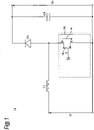
- Fig. 1 is a block diagram illustrating a configuration example of a boost chopper circuit 1 according to a first embodiment.
- the boost chopper circuit 1 includes a current-driven switching circuit 10 having a semiconductor switch 14 of a switching element, an inductor L1, a diode D1, and a capacitor C1.
- an input voltage Vi is applied to the connection point of the anode of the diode D1 and the drain of the semiconductor switch 14 via the inductor L1.
- the source of the semiconductor switch 14 is grounded.
- the cathode of the diode D1 is connected to one end of the capacitor C1 that outputs an output voltage Vo, and the other end of the capacitor is grounded.
- a switching drive signal (hereinafter, referred to as a drive signal) for the boost chopper is inputted to the gate of the semiconductor switch 14, and the semiconductor switch 14 is switched to be turned on or off.
- the inductor L1 generates electromotive force in a direction that prevents a change in current. Therefore, when the semiconductor switch 14 is switched from on to off, the inductor L1 generates electromotive force in the same direction as the input voltage Vi so as to prevent the current from decreasing by the resistance of the diode D1. As a result, a voltage higher than the input voltage Vi is generated, and the voltage is smoothed by the capacitor C1 and converted into the output voltage Vo. Therefore, by periodically and selectively switching on and off of the semiconductor switch 14, the boost chopper circuit 1 converts the input voltage Vi into the DC output voltage Vo higher than the input voltage Vi and outputs the DC output voltage Vo.
- the current-driven switching circuit 10 of the boost chopper circuit 1 includes an overcurrent protection circuit 11 that turns off the semiconductor switch 14 and cuts off the overcurrent by grounding the gate of the semiconductor switch 14 in order to protect the semiconductor switch 14 from breaking due to a drain current Id that is the overcurrent of a predetermined value or more from flowing between the drain and the source of the semiconductor switch 14.
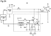
- Fig. 2A is a block diagram illustrating a detailed configuration example of the current-driven switching circuit 10 in Fig. 1 .
- the current-driven switching circuit 10 includes the overcurrent protection circuit 11, a controller unit 12, a drive unit 13, the semiconductor switch 14, and a resistor R1.
- the overcurrent protection circuit 11 includes transistors Q1 and Q2, a pull-up resistor R2, a voltage detector circuit 15, a capacitor C11, and a resistor R11.
- the overcurrent protection circuit 11 turns off the semiconductor switch 14 and cuts off the overcurrent by grounding the gate of the semiconductor switch 14 in order to protect the semiconductor switch 14 from breaking due to the drain current Id that is the overcurrent of a predetermined value or more from flowing between the drain and the source of the semiconductor switch 14.
- the controller unit 12 controls the drive unit 13 by a drive signal Sdrv that is a pulse signal.
- the voltage detector circuit 15 monitors a detection voltage Vgs1 to be inputted, and outputs an abnormality detection signal Sa of the high level to the controller unit 12 when the detection voltage Vgs1 becomes a predetermined threshold value or more.
- the controller unit 12 fixes the drive signal Sdrv to the low level and stops the drive unit 13.
- a base voltage of the transistor Q2 is denoted as Vocp.
- the drive unit 13 applies a gate-source voltage Vgs14 to the gate of the semiconductor switch 14 via the resistor R1 based on the drive signal Sdrv from the controller unit 12, and controls the semiconductor switch 14 to be turned on and off.
- the semiconductor switch 14 is, for example, a switching element such as a GaN device, and is controlled to be turned and off by the drive unit 13 to selectively switch whether or not to conduct the drain current Id.
- the transistor Q1 is, for example, an N-channel field effect transistor (FET).
- FET field effect transistor
- the drain of the transistor Q1 is connected to the gate-source voltage Vgs14, the source of the transistor Q1 is grounded, and the gate of the transistor Q1 is connected to the collector of the transistor Q2.
- the transistor Q2 is, for example, a PNP bipolar transistor, the emitter of the transistor Q2 is connected to the gate-source voltage Vgsl4, the collector of the transistor Q2 is grounded via a time constant circuit 19 which is a parallel circuit of the capacitor C11 and the resistor R11, and the base of the transistor Q2 is pulled up to a threshold voltage VTH via the pull-up resistor R2.
- the time constant circuit 19 is provided to discharge a gate-source voltage Vgs of the transistor Q1 by the time constant thereof in order to return the overcurrent protection circuit 11 from a protection operation to a steady operation after the stop of the drive signal Sdrv.
- the threshold voltage VTH is an example of a "pull-up voltage” of the present invention
- the resistor R11 is an example of a "ground circuit” of the present invention.
- both the transistors Q1 and Q2 are turned off, and at this point, the detection voltage Vgs1 is held at a predetermined voltage.
- the transistor Q2 is turned on, and further, when the gate-source voltage Vgs14 exceeds the threshold voltage VTH due to the continuation of the short circuit, the transistor Q1 is also turned on, and the protection operation starts.
- the voltage detector circuit 15 detects the detection voltage Vgs1, which is the gate-source voltage of the transistor Q1, and outputs a signal indicating the detection voltage Vgs1 to the controller unit 12.
- the protection operation starts and the detection voltage Vgs falls below the threshold voltage VTH, the transistor Q2 is turned off.
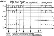
- Fig. 3A is a timing chart illustrating operation waveforms of signals and the like in the current-driven switching circuit 10 in Fig. 1 .
- the current-driven switching circuit 10 starts operation at time t0, a short circuit occurs in the semiconductor switch 14 at time t1, and then, the controller unit 12 detects the short circuit at time t3.
- the time interval from the time t0 to the time t1 is referred to as a steady operation time interval
- the time interval from the time t1 to time t2 is referred to as a protection operation time interval
- the time interval from the time t2 to the time t3 is referred to as a protection holding time interval
- the time interval from the time t3 to time t5 is referred to as a Vgs1-OFF time interval
- the process returns to the steady operation time interval from time t6.
- the detection voltage Vgs1 is the threshold voltage VTH. Because the threshold voltage VTH is set higher than the gate-source voltage Vgs14 supplied by the drive unit 13 when the drive signal Sdrv is at the high level, both the transistors Q1 and Q2 are always turned off during the steady operation time interval.
- a gate-source voltage of a semiconductor switch included in the semiconductor device overshoots (instantaneously rises). Also in the present embodiment, at the time t1 in Fig. 3A , the drain current Id flowing through the semiconductor switch 14 excessively increases, and the gate-source voltage Vgs14 of the semiconductor switch 14 rapidly increases and becomes a value higher than the threshold voltage VTH. As a result, the transistor Q2 is turned on, and thus the transistor Q1 is also turned on.
- the gate-source voltage Vgs14 is discharged by the transistor Q1 and becomes zero.
- the semiconductor switch 14 is turned off, the overcurrent flowing through the semiconductor switch 14 can be stopped, and the overcurrent protection circuit 11 can start the protection operation.
- the time from the occurrence of the short circuit at the time t1 until the overcurrent protection circuit 11 starts the protection operation includes a delay in switching of the transistors Q1 and Q2, and is short, for example, about 20 to 100 nanoseconds.
- the protection holding function according to the present embodiment is performed by the time constant circuit 19 connected to the gate terminal of the transistor Q1.
- the voltage detector circuit 15 outputs to the controller unit 12 an abnormality detection signal Sa of the H level based on the detection voltage Vgs1. In response to this, the controller unit 12 determines that the protection operation has been performed and stops the output of the drive signal Sdrv (time t3). In a stop time interval Ph, the drive signal Sdrv is always at the low level, and the semiconductor switch 14 is always kept to be turned off.
- time t4 When an abnormal state is eliminated in a protection state (time t4), after the stop of the drive signal, the time constant circuit 19 discharges the gate-source voltage Vgs of the transistor Q1 by the time constant thereof in order to return the overcurrent protection circuit 11 from the protection operation to the steady operation. As a result, the transistor Q1 is turned off (time t5) and the process returns to the steady operation.
- Fig. 3B is a timing chart illustrating a simulation result of the current-driven switching circuit 10 in Fig. 1 and illustrating operation waveforms of the current and voltage thereof.
- the gate-source voltage Vgs 14 can be controlled without any large overshoot.
- the overcurrent protection circuit 11 includes the pull-up resistor R2, the transistor Q1 which is an N-channel FET, the transistor Q2 which is a PNP bipolar transistor, the voltage detector circuit 15, and the time constant circuit 19 including the capacitor C11 and the resistor R11.
- the transistors Q2 and Q1 are sequentially turned on.
- the transistor Q1 instantaneously decreases the gate-source voltage Vgs14 to 0 V to start the protection operation of turning off the semiconductor switch.
- the controller unit 12 stops the drive unit 13, and turns off the semiconductor switch 14. Therefore, according to the present embodiment, the overcurrent flowing through the semiconductor switch 14 can be stopped more quickly than the prior art, and the semiconductor switch 14 can be protected.
- Fig. 2B is a block diagram illustrating a detailed configuration example of a current-driven switching circuit 10a according to a modified embodiment of the first embodiment.
- the current-driven switching circuit 10a in Fig. 2B includes an overcurrent protection circuit 11a instead of the overcurrent protection circuit 11 in Fig. 2A , and is different in that a noise removal diode D2 is provided in the resistor R2. It is noted that this modified embodiment can also be applied to embodiments other than the first embodiment.
- a threshold voltage Vocp temporarily rises as illustrated in Fig. 3B .
- a delay occurs due to fluctuation of the threshold voltage Vocp, which causes a delay in the start of the protection operation.
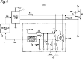
- Fig. 4 is a block diagram illustrating a configuration example of a current-driven switching circuit 10A according to a second embodiment. Referring to Fig. 4 , the current-driven switching circuit 10A is different from the current-driven switching circuit 10 in the following points.
- the short circuit occurs in the semiconductor switch 14, and the gate-source voltage Vgs14 rapidly rises.
- the threshold voltage Vocp temporarily increases as the gate-source voltage Vgsl4 rises, but this change is reduced by the capacitor Ca. Therefore, the delay in the start of the protection operation can be suppressed.
- Fig. 5 is a timing chart illustrating a simulation result of the current-driven switching circuit 10A in Fig. 4 and illustrating operation waveforms of the current and voltage thereof. As is apparent from Fig. 5 , the threshold voltage Vocp can be controlled without a large temporary rise.
- the overcurrent protection circuit 11A further includes the capacitor Ca in addition to the overcurrent protection circuit 11.
- the temporary rise of the threshold voltage Vocp due to the rise of the gate-source voltage Vgs14 can be made smaller than that of the overcurrent protection circuit 11 in Fig. 2A , and the delay at the start of the protection operation can be reduced as compared with the overcurrent protection circuit 11.
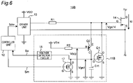
- Fig. 6 is a block diagram illustrating a configuration example of a current-driven switching circuit 10B according to a third embodiment.
- the current-driven switching circuit 10B is different from the current-driven switching circuit 10A in Fig. 4 in the following point.
- the current-driven switching circuit 10B includes, instead of the resistor R11, a transistor 17 that is, for example, an N-channel MOSFET and operates as a ground circuit.
- a return signal Sm from the controller unit 12 is inputted to the gate of the transistor 17, the drain of the transistor 17 is connected to the gate of the transistor Q1, and the source of the transistor 17 is grounded.
- the controller unit 12 outputs the return signal Sm to the gate of the transistor 17 in order to return the overcurrent protection circuit 11 from the protection operation to the steady operation. Accordingly, the gate-source voltage Vgs1 of the transistor Q1 is discharged by turning on the transistor 17.
- Fig. 7 is a timing chart illustrating operation waveforms of signals and the like in the current-driven switching circuit 10B in Fig. 6 .
- the current-driven switching circuit 10B is different from the current-driven switching circuit 10A in Fig. 4 in the following points.
- the current-driven switching circuit 10B includes the transistor 17. After determining that the abnormal state has been eliminated (time t11) and after a predetermined time time interval (time t4), the controller unit 12 outputs the return signal Sm to the gate of the transistor 17. As a result, the transistor 17 is turned on, and the gate-source voltage Vgs of the transistor Q1 is discharged to cause the transistor Q1 to be turned off, and the semiconductor switch 14 returns from the protection state to the steady state (at time T6).
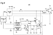
- Fig. 8 is a block diagram illustrating a configuration example of a current-driven switching circuit 10C according to a fourth embodiment. Referring to Fig. 8 , the current-driven switching circuit 10C is different from the current-driven switching circuit 10B in Fig. 6 in the following points.
- the controller unit 12 controls a base current Itr of the transistor 17a via the transistor drive unit 16 to control the transistor 17a to be turned on and off. As a result, the same effects as those of the third embodiment can be obtained.
- the boost chopper circuit 1 has been described as a semiconductor device including the current-driven switching circuits 10 and 10A to 10C according to the present invention.
- the present invention is not limited thereto, and can be used for a circuit, an apparatus, and the like that perform switching control of a current with a semiconductor switch.
- Fig. 9 is a block diagram illustrating a configuration example of a half-bridge inverter circuit 1A according to a first modified embodiment.
- the half-bridge inverter circuit 1A includes an inductor L2, the two current-driven switching circuits 10, and a capacitor C2.
- the semiconductor switches 14 of the two current-driven switching circuits 10 are controlled to be turned on time intervalically and alternately.
- an input voltage Vi is switched, smoothed by the capacitor C2, and converted into an alternating current (AC) output voltage Vo.
- the half-bridge inverter circuit 1A switches a DC input voltage Vi, converts the DC input voltage Vi into the AC output voltage Vo, and outputs the AC output voltage Vo.
- Each of the two current-driven switching circuits 10 may be replaced with any one of the current-driven switching circuits 10A to 10C.
- Fig. 10 is a block diagram illustrating a configuration example of a full-bridge inverter circuit 1B according to a second modified embodiment.
- the full-bridge inverter circuit 1B includes a capacitor C3, four current-driven switching circuits 10, and inductors L3 and L4.
- the four current-driven switching circuits 10 are controlled such that a time interval in which the first and fourth current-driven switching circuits 10 (upper left and lower right in the drawing) are turned on and the second and third current-driven switching circuits 10 (lower left and upper right in the drawing) are turned off and a time interval in which these on and off of the current-driven switching circuits are reversed time intervalically and alternately appear.
- an input voltage Vi is switched, and the switched input voltage Vi is smoothed by the capacitor C3 and the inductors L3 and L4.
- the full-bridge inverter circuit 1B switches the DC input voltage Vi, converts the DC input voltage Vi into an AC output voltage Vo, and outputs the AC output voltage Vo.
- Each of the four current-driven switching circuits 10 may be replaced with any one of the current-driven switching circuits 10A to 10C.
- the current-driven switching circuit and the overcurrent protection circuit according to the present invention can be used for a circuit and an apparatus that perform switching control of a current in a semiconductor device.
- the pull-up resistor R2 is used as means for limiting the current from the power supply of the threshold voltage VTH.
- the present invention is not limited thereto, and a diode or the like may be used instead of the pull-up resistor R2.
- the current-driven switching circuits 10 and 10A to 10C are used as the switching circuits.
- the present invention is not limited thereto, and a voltage-driven switching circuit may be used instead of the current-driven switching circuit.
Landscapes
- Engineering & Computer Science (AREA)
- Power Engineering (AREA)
- Dc-Dc Converters (AREA)
- Power Conversion In General (AREA)
- Electronic Switches (AREA)
- Protection Of Static Devices (AREA)
- Inverter Devices (AREA)
Abstract
Description
- The present invention relates to an overcurrent protection circuit and a switching circuit. In this case, the switching circuit is, for example, a switching circuit such as a boost chopper circuit, a half-bridge inverter circuit, or a full-bridge inverter circuit.
- A semiconductor device generally has a short circuit tolerance, and when a current exceeding the short circuit tolerance flows, the semiconductor device may be broken. Overcurrent protection of the semiconductor device can be performed by quickly detecting an overcurrent flowing through the semiconductor device due to a short circuit and stopping the current flowing through the semiconductor device.
- For example,
Patent Document 1 provides an overcurrent protector for a power converter, in which the overcurrent protector can change a set level of a detection voltage of collector short-circuit detection at an optional timing even when a direct current (DC) voltage is high, low, or a constant, and can reliably protect a voltage drive element from the overcurrent. - The overcurrent protector according to
Patent Document 1 includes: - the power converter having a voltage-driven power switching element;
- an overcurrent detection section that detects a voltage of an input-side main terminal of the power switching element and applies an off signal to the power switching element when the voltage exceeds a predetermined value; and
- an overcurrent setting section that can be connected to the overcurrent detection section in a parallel relationship at an optional timing and can change the predetermined value.
- A GaN device is a semiconductor device using gallium nitride (GaN), and has such a feature that the semiconductor device can be driven at a higher frequency than that of a conventional semiconductor device such as an insulated gate bipolar transistor (IGBT) and a silicon carbide (SiC) device.
- [Patent Document 1]
Japanese Patent Laid-open Publication No. JP2006-14402A - However, the GaN device is weaker in overcurrent than the conventional semiconductor device, and there is a possibility of being broken by the overcurrent of, for example, about 100 nanoseconds. Therefore, the conventional overcurrent protection techniques such as desaturation (DESAT) detection, current transformer (CT) detection, or the technique of
Patent Document 1 cannot sufficiently protect the GaN devices. - An object of the present invention is to solve the above problems and to provide an overcurrent protection circuit and a switching circuit that can protect a semiconductor switch from the overcurrent more quickly than the prior art.
- According to one aspect of the present invention, there is provided an overcurrent protection circuit for protecting an overcurrent flowing through a switching element that is controlled to be turned on and off based on a drive signal. The overcurrent protection circuit includes: a first transistor that is an N-channel field effect transistor (FET) having a drain connected to a control terminal of the switching element and a grounded source; a second transistor that is a PNP bipolar transistor having an emitter connected to the control terminal of the switching element, a collector connected to a gate of the first transistor and grounded via a first capacitor, and a base pulled up to a predetermined pull-up voltage; and a ground circuit connected in parallel with the first capacitor.
- According to the overcurrent protection circuit according to the present invention, the semiconductor device can be protected from the overcurrent more quickly than the prior art.
-
-
Fig. 1 is a block diagram illustrating a configuration example of aboost chopper circuit 1 according to a first embodiment. -
Fig. 2A is a block diagram illustrating a detailed configuration example of a current-drivenswitching circuit 10 inFig. 1 . -
Fig. 2B is a block diagram illustrating a detailed configuration example of a current-drivenswitching circuit 10a according to a modified embodiment of the first embodiment. -
Fig. 3A is a timing chart illustrating operation waveforms of signals and the like in the current-drivenswitching circuit 10 inFig. 1 . -
Fig. 3B is a timing chart illustrating a simulation result of the current-drivenswitching circuit 10 inFig. 1 and illustrating operation waveforms of the current and voltage thereof. -
Fig. 4 is a block diagram illustrating a configuration example of a current-drivenswitching circuit 10A according to a second embodiment. -
Fig. 5 is a timing chart illustrating a simulation result of the current-drivenswitching circuit 10A inFig. 4 and illustrating operation waveforms of the current and voltage thereof. -
Fig. 6 is a block diagram illustrating a configuration example of a current-drivenswitching circuit 10B according to a third embodiment. -
Fig. 7 is a timing chart illustrating operation waveforms of signals and the like in the current-drivenswitching circuit 10B inFig. 6 . -
Fig. 8 is a block diagram illustrating a configuration example of a current-drivenswitching circuit 10C according to a fourth embodiment. -
Fig. 9 is a block diagram illustrating a configuration example of a half-bridge inverter circuit 1A according to a first modified embodiment. -
Fig. 10 is a block diagram illustrating a configuration example of a full-bridge inverter circuit 1B according to a second modified embodiment. - Hereinafter, embodiments according to the present invention are described with reference to the drawings. However, each of the embodiments described below is merely an example of the present invention in all respects. It goes without saying that various improvements and modifications can be made without departing from the scope of the present invention. That is, in carrying out the present invention, specific configurations according to the embodiments may be appropriately adopted.
-
Fig. 1 is a block diagram illustrating a configuration example of aboost chopper circuit 1 according to a first embodiment. Referring toFig. 1 , theboost chopper circuit 1 includes a current-drivenswitching circuit 10 having asemiconductor switch 14 of a switching element, an inductor L1, a diode D1, and a capacitor C1. - Referring to
Fig. 1 , an input voltage Vi is applied to the connection point of the anode of the diode D1 and the drain of thesemiconductor switch 14 via the inductor L1. The source of thesemiconductor switch 14 is grounded. The cathode of the diode D1 is connected to one end of the capacitor C1 that outputs an output voltage Vo, and the other end of the capacitor is grounded. A switching drive signal (hereinafter, referred to as a drive signal) for the boost chopper is inputted to the gate of thesemiconductor switch 14, and thesemiconductor switch 14 is switched to be turned on or off. - In the
boost chopper circuit 1 configured as described above, the inductor L1 generates electromotive force in a direction that prevents a change in current. Therefore, when thesemiconductor switch 14 is switched from on to off, the inductor L1 generates electromotive force in the same direction as the input voltage Vi so as to prevent the current from decreasing by the resistance of the diode D1. As a result, a voltage higher than the input voltage Vi is generated, and the voltage is smoothed by the capacitor C1 and converted into the output voltage Vo. Therefore, by periodically and selectively switching on and off of thesemiconductor switch 14, theboost chopper circuit 1 converts the input voltage Vi into the DC output voltage Vo higher than the input voltage Vi and outputs the DC output voltage Vo. - As is described in detail later with reference to
Fig. 2 , the current-drivenswitching circuit 10 of theboost chopper circuit 1 includes anovercurrent protection circuit 11 that turns off thesemiconductor switch 14 and cuts off the overcurrent by grounding the gate of thesemiconductor switch 14 in order to protect thesemiconductor switch 14 from breaking due to a drain current Id that is the overcurrent of a predetermined value or more from flowing between the drain and the source of thesemiconductor switch 14. -
Fig. 2A is a block diagram illustrating a detailed configuration example of the current-drivenswitching circuit 10 inFig. 1 . Referring toFig. 2A , the current-drivenswitching circuit 10 includes theovercurrent protection circuit 11, acontroller unit 12, adrive unit 13, thesemiconductor switch 14, and a resistor R1. Theovercurrent protection circuit 11 includes transistors Q1 and Q2, a pull-up resistor R2, avoltage detector circuit 15, a capacitor C11, and a resistor R11. In this case, theovercurrent protection circuit 11 turns off thesemiconductor switch 14 and cuts off the overcurrent by grounding the gate of thesemiconductor switch 14 in order to protect thesemiconductor switch 14 from breaking due to the drain current Id that is the overcurrent of a predetermined value or more from flowing between the drain and the source of thesemiconductor switch 14. - Referring to
Fig. 2A , thecontroller unit 12 controls thedrive unit 13 by a drive signal Sdrv that is a pulse signal. In addition, thevoltage detector circuit 15 monitors a detection voltage Vgs1 to be inputted, and outputs an abnormality detection signal Sa of the high level to thecontroller unit 12 when the detection voltage Vgs1 becomes a predetermined threshold value or more. In response to this, thecontroller unit 12 fixes the drive signal Sdrv to the low level and stops thedrive unit 13. Note that a base voltage of the transistor Q2 is denoted as Vocp. - The
drive unit 13 applies a gate-source voltage Vgs14 to the gate of thesemiconductor switch 14 via the resistor R1 based on the drive signal Sdrv from thecontroller unit 12, and controls thesemiconductor switch 14 to be turned on and off. Thesemiconductor switch 14 is, for example, a switching element such as a GaN device, and is controlled to be turned and off by thedrive unit 13 to selectively switch whether or not to conduct the drain current Id. - In the
overcurrent protection circuit 11, the transistor Q1 is, for example, an N-channel field effect transistor (FET). The drain of the transistor Q1 is connected to the gate-source voltage Vgs14, the source of the transistor Q1 is grounded, and the gate of the transistor Q1 is connected to the collector of the transistor Q2. In addition, the transistor Q2 is, for example, a PNP bipolar transistor, the emitter of the transistor Q2 is connected to the gate-source voltage Vgsl4, the collector of the transistor Q2 is grounded via a timeconstant circuit 19 which is a parallel circuit of the capacitor C11 and the resistor R11, and the base of the transistor Q2 is pulled up to a threshold voltage VTH via the pull-up resistor R2. In this case, the timeconstant circuit 19 is provided to discharge a gate-source voltage Vgs of the transistor Q1 by the time constant thereof in order to return theovercurrent protection circuit 11 from a protection operation to a steady operation after the stop of the drive signal Sdrv. Note that the threshold voltage VTH is an example of a "pull-up voltage" of the present invention, and the resistor R11 is an example of a "ground circuit" of the present invention. - In this case, in a steady operation time interval, both the transistors Q1 and Q2 are turned off, and at this point, the detection voltage Vgs1 is held at a predetermined voltage. Next, when the gate-source voltage Vgs14 becomes the threshold voltage VTH due to the occurrence of the short circuit, the transistor Q2 is turned on, and further, when the gate-source voltage Vgs14 exceeds the threshold voltage VTH due to the continuation of the short circuit, the transistor Q1 is also turned on, and the protection operation starts. At this point, the
voltage detector circuit 15 detects the detection voltage Vgs1, which is the gate-source voltage of the transistor Q1, and outputs a signal indicating the detection voltage Vgs1 to thecontroller unit 12. Next, when the protection operation starts and the detection voltage Vgs falls below the threshold voltage VTH, the transistor Q2 is turned off. -
Fig. 3A is a timing chart illustrating operation waveforms of signals and the like in the current-drivenswitching circuit 10 inFig. 1 . - Referring to
Fig. 3A , the current-drivenswitching circuit 10 starts operation at time t0, a short circuit occurs in thesemiconductor switch 14 at time t1, and then, thecontroller unit 12 detects the short circuit at time t3. In this case, the time interval from the time t0 to the time t1 is referred to as a steady operation time interval, the time interval from the time t1 to time t2 is referred to as a protection operation time interval, the time interval from the time t2 to the time t3 is referred to as a protection holding time interval, the time interval from the time t3 to time t5 is referred to as a Vgs1-OFF time interval, and the process returns to the steady operation time interval from time t6. - In the steady operation time interval, because no current flows through the pull-up resistor R2 except for the time interval in which the detection voltage Vgs1 overshoots (to be described in detail later), the detection voltage Vgs1 is the threshold voltage VTH. Because the threshold voltage VTH is set higher than the gate-source voltage Vgs14 supplied by the
drive unit 13 when the drive signal Sdrv is at the high level, both the transistors Q1 and Q2 are always turned off during the steady operation time interval. - In general, when an overcurrent flows through a semiconductor device, a gate-source voltage of a semiconductor switch included in the semiconductor device overshoots (instantaneously rises). Also in the present embodiment, at the time t1 in
Fig. 3A , the drain current Id flowing through thesemiconductor switch 14 excessively increases, and the gate-source voltage Vgs14 of thesemiconductor switch 14 rapidly increases and becomes a value higher than the threshold voltage VTH. As a result, the transistor Q2 is turned on, and thus the transistor Q1 is also turned on. - Therefore, the gate-source voltage Vgs14 is discharged by the transistor Q1 and becomes zero. As a result, because the
semiconductor switch 14 is turned off, the overcurrent flowing through thesemiconductor switch 14 can be stopped, and theovercurrent protection circuit 11 can start the protection operation. The time from the occurrence of the short circuit at the time t1 until theovercurrent protection circuit 11 starts the protection operation includes a delay in switching of the transistors Q1 and Q2, and is short, for example, about 20 to 100 nanoseconds. - In addition, the protection holding function according to the present embodiment is performed by the time
constant circuit 19 connected to the gate terminal of the transistor Q1. - The
voltage detector circuit 15 outputs to thecontroller unit 12 an abnormality detection signal Sa of the H level based on the detection voltage Vgs1. In response to this, thecontroller unit 12 determines that the protection operation has been performed and stops the output of the drive signal Sdrv (time t3). In a stop time interval Ph, the drive signal Sdrv is always at the low level, and thesemiconductor switch 14 is always kept to be turned off. - Because the protection operation is held until the detection voltage Vgs1 is completely discharged by the time
constant circuit 19, any repeated overcurrent does not occur. - When an abnormal state is eliminated in a protection state (time t4), after the stop of the drive signal, the time
constant circuit 19 discharges the gate-source voltage Vgs of the transistor Q1 by the time constant thereof in order to return theovercurrent protection circuit 11 from the protection operation to the steady operation. As a result, the transistor Q1 is turned off (time t5) and the process returns to the steady operation. -
Fig. 3B is a timing chart illustrating a simulation result of the current-drivenswitching circuit 10 inFig. 1 and illustrating operation waveforms of the current and voltage thereof. As is clear fromFig. 3B , the gate-source voltage Vgs 14 can be controlled without any large overshoot. - As described above, the
overcurrent protection circuit 11 according to the present embodiment includes the pull-up resistor R2, the transistor Q1 which is an N-channel FET, the transistor Q2 which is a PNP bipolar transistor, thevoltage detector circuit 15, and the timeconstant circuit 19 including the capacitor C11 and the resistor R11. When the gate-source voltage Vgs14 of thesemiconductor switch 14 exceeds the threshold voltage VTH, the transistors Q2 and Q1 are sequentially turned on. As a result, the transistor Q1 instantaneously decreases the gate-source voltage Vgs14 to 0 V to start the protection operation of turning off the semiconductor switch. In addition, based on the abnormality detection signal Sa from thevoltage detector circuit 15, thecontroller unit 12 stops thedrive unit 13, and turns off thesemiconductor switch 14. Therefore, according to the present embodiment, the overcurrent flowing through thesemiconductor switch 14 can be stopped more quickly than the prior art, and thesemiconductor switch 14 can be protected. -
Fig. 2B is a block diagram illustrating a detailed configuration example of a current-drivenswitching circuit 10a according to a modified embodiment of the first embodiment. The current-drivenswitching circuit 10a inFig. 2B includes anovercurrent protection circuit 11a instead of theovercurrent protection circuit 11 inFig. 2A , and is different in that a noise removal diode D2 is provided in the resistor R2. It is noted that this modified embodiment can also be applied to embodiments other than the first embodiment. - In the first embodiment, when the gate-source voltage Vgs14 of the
semiconductor switch 14 rises, a threshold voltage Vocp temporarily rises as illustrated inFig. 3B . At this time, a delay occurs due to fluctuation of the threshold voltage Vocp, which causes a delay in the start of the protection operation. -
Fig. 4 is a block diagram illustrating a configuration example of a current-drivenswitching circuit 10A according to a second embodiment. Referring toFig. 4 , the current-drivenswitching circuit 10A is different from the current-drivenswitching circuit 10 in the following points. - (1) An
overcurrent protection circuit 11A further includes a capacitor Ca connected to the base of a transistor Q2. - (2) The power supply having the threshold voltage VTH charges the capacitor Ca to the threshold voltage VTH via a pull-up resistor R2.
- In the second embodiment, the short circuit occurs in the
semiconductor switch 14, and the gate-source voltage Vgs14 rapidly rises. At this time, the threshold voltage Vocp temporarily increases as the gate-source voltage Vgsl4 rises, but this change is reduced by the capacitor Ca. Therefore, the delay in the start of the protection operation can be suppressed. -
Fig. 5 is a timing chart illustrating a simulation result of the current-drivenswitching circuit 10A inFig. 4 and illustrating operation waveforms of the current and voltage thereof. As is apparent fromFig. 5 , the threshold voltage Vocp can be controlled without a large temporary rise. - As described above, the
overcurrent protection circuit 11A according to the present embodiment further includes the capacitor Ca in addition to theovercurrent protection circuit 11. As a result, the temporary rise of the threshold voltage Vocp due to the rise of the gate-source voltage Vgs14 can be made smaller than that of theovercurrent protection circuit 11 inFig. 2A , and the delay at the start of the protection operation can be reduced as compared with theovercurrent protection circuit 11. -
Fig. 6 is a block diagram illustrating a configuration example of a current-drivenswitching circuit 10B according to a third embodiment. - Referring to
Fig. 6 , the current-drivenswitching circuit 10B is different from the current-drivenswitching circuit 10A inFig. 4 in the following point.
(1) The current-drivenswitching circuit 10B includes, instead of the resistor R11, atransistor 17 that is, for example, an N-channel MOSFET and operates as a ground circuit. - Referring to
Fig. 6 , a return signal Sm from thecontroller unit 12 is inputted to the gate of thetransistor 17, the drain of thetransistor 17 is connected to the gate of the transistor Q1, and the source of thetransistor 17 is grounded. After the stop of a drive signal, thecontroller unit 12 outputs the return signal Sm to the gate of thetransistor 17 in order to return theovercurrent protection circuit 11 from the protection operation to the steady operation. Accordingly, the gate-source voltage Vgs1 of the transistor Q1 is discharged by turning on thetransistor 17. -
Fig. 7 is a timing chart illustrating operation waveforms of signals and the like in the current-drivenswitching circuit 10B inFig. 6 . - Referring to
Fig. 7 , the current-drivenswitching circuit 10B is different from the current-drivenswitching circuit 10A inFig. 4 in the following points. - (1) When the short circuit occurs at time t1, the gate voltage of the transistor Q1 rises, and the protection operation starts.
- (2) At time t3, the
controller unit 12 detects an abnormal state from avoltage detector circuit 15 based on an abnormality detection signal Sa, and then, determines that the abnormal state has been eliminated when the abnormality detection signal Sa decreases to the low level (at time t11), and then, outputs the return signal Sm to the gate of thetransistor 17 after a predetermined time time interval (time t4). As a result, thetransistor 17 is turned on, and the gate-source voltage Vgs of the transistor Q1 is discharged to cause the transistor Q1 to be turned off, and thesemiconductor switch 14 returns from the protection state to the steady state (at time T6). - As described above, the current-driven
switching circuit 10B according to the third embodiment includes thetransistor 17. After determining that the abnormal state has been eliminated (time t11) and after a predetermined time time interval (time t4), thecontroller unit 12 outputs the return signal Sm to the gate of thetransistor 17. As a result, thetransistor 17 is turned on, and the gate-source voltage Vgs of the transistor Q1 is discharged to cause the transistor Q1 to be turned off, and thesemiconductor switch 14 returns from the protection state to the steady state (at time T6). -
Fig. 8 is a block diagram illustrating a configuration example of a current-drivenswitching circuit 10C according to a fourth embodiment. Referring toFig. 8 , the current-drivenswitching circuit 10C is different from the current-drivenswitching circuit 10B inFig. 6 in the following points. - (1) Instead of the
transistor 17 which is an N-channel MOSFET, for example, atransistor 17a which is an NPN bipolar transistor is provided. - (2) A
transistor drive unit 16 is provided between acontroller unit 12 and the gate of thetransistor 17a. - Referring to
Fig. 8 , thecontroller unit 12 controls a base current Itr of thetransistor 17a via thetransistor drive unit 16 to control thetransistor 17a to be turned on and off. As a result, the same effects as those of the third embodiment can be obtained. - Although the embodiments of the present invention have been described in details above, the above description is merely an example of the present invention in all respects. It goes without saying that various improvements and modifications can be made without departing from the scope of the present invention. For example, the following modifications are possible. In the following description, the same reference characters are used for the same components as those of the above embodiments, and the description of the same points as those of the above embodiments is appropriately omitted. The following modified embodiments can be appropriately combined.
- In the first to fourth embodiments, the
boost chopper circuit 1 has been described as a semiconductor device including the current-drivenswitching circuits - For example,
Fig. 9 is a block diagram illustrating a configuration example of a half-bridge inverter circuit 1A according to a first modified embodiment. Referring toFig. 9 , the half-bridge inverter circuit 1A includes an inductor L2, the two current-drivenswitching circuits 10, and a capacitor C2. - Referring to
Fig. 9 , the semiconductor switches 14 of the two current-drivenswitching circuits 10 are controlled to be turned on time intervalically and alternately. As a result, an input voltage Vi is switched, smoothed by the capacitor C2, and converted into an alternating current (AC) output voltage Vo. As a result, the half-bridge inverter circuit 1A switches a DC input voltage Vi, converts the DC input voltage Vi into the AC output voltage Vo, and outputs the AC output voltage Vo. Each of the two current-drivenswitching circuits 10 may be replaced with any one of the current-drivenswitching circuits 10A to 10C. - In addition,
Fig. 10 is a block diagram illustrating a configuration example of a full-bridge inverter circuit 1B according to a second modified embodiment. Referring toFig. 10 , the full-bridge inverter circuit 1B includes a capacitor C3, four current-drivenswitching circuits 10, and inductors L3 and L4. - Referring to
Fig. 10 , the four current-drivenswitching circuits 10 are controlled such that a time interval in which the first and fourth current-driven switching circuits 10 (upper left and lower right in the drawing) are turned on and the second and third current-driven switching circuits 10 (lower left and upper right in the drawing) are turned off and a time interval in which these on and off of the current-driven switching circuits are reversed time intervalically and alternately appear. As a result, an input voltage Vi is switched, and the switched input voltage Vi is smoothed by the capacitor C3 and the inductors L3 and L4. As a result, the full-bridge inverter circuit 1B switches the DC input voltage Vi, converts the DC input voltage Vi into an AC output voltage Vo, and outputs the AC output voltage Vo. Each of the four current-drivenswitching circuits 10 may be replaced with any one of the current-drivenswitching circuits 10A to 10C. - As described above, the current-driven switching circuit and the overcurrent protection circuit according to the present invention can be used for a circuit and an apparatus that perform switching control of a current in a semiconductor device.
- In addition, in the first to fourth embodiments, the pull-up resistor R2 is used as means for limiting the current from the power supply of the threshold voltage VTH. However, the present invention is not limited thereto, and a diode or the like may be used instead of the pull-up resistor R2. Further, in the first to fourth embodiments, the current-driven
switching circuits -
- 1: BOOST CHOPPER CIRCUIT
- 1A: HALF-BRIDGE INVERTER CIRCUIT
- 1B: FULL-BRIDGE INVERTER CIRCUIT
- 10, 10a, 10A to 10C: CURRENT-DRIVEN SWITCHING CIRCUIT
- 11, 11a, 11A to 11C: OVERCURRENT PROTECTION CIRCUIT
- 12: CONTROLLER UNIT
- 13: DRIVE UNIT
- 14: SEMICONDUCTOR SWITCH
- 15: VOLTAGE DETECTOR CIRCUIT
- 16: TRANSISTOR DRIVE UNIT
- 17, 17a: TRANSISTOR
- 18, 19: TIME CONSTANT CIRCUIT
- C1 to C11: CAPACITOR
- D1, D2: DIODE
- L1, L2: REACTOR
- Q1, Q2: TRANSISTOR
- R1 to R11: RESISTOR
Claims (12)
- An overcurrent protection circuit for protecting an overcurrent flowing through a switching element that is controlled to be turned on and off based on a drive signal, the overcurrent protection circuit comprising:a first transistor that is an N-channel field effect transistor (FET) having a drain connected to a control terminal of the switching element and a grounded source;a second transistor that is a PNP bipolar transistor having an emitter connected to the control terminal of the switching element, a collector connected to a gate of the first transistor and grounded via a first capacitor, and a base pulled up to a predetermined pull-up voltage; anda ground circuit connected in parallel with the first capacitor.
- The overcurrent protection circuit as claimed in claim 1,wherein the ground circuit is a first resistor, andwherein the first capacitor and the first resistor configures a first time constant circuit.
- The overcurrent protection circuit as claimed in claim 1, wherein the ground circuit is a third transistor that is an FET including a drain and a source connected in parallel with the first capacitor, and a gate applied with a return signal for returning the overcurrent protection circuit from a protection operation to a steady operation.
- The overcurrent protection circuit as claimed in claim 1, wherein the ground circuit is a fourth transistor that is a bipolar transistor including a collector and an emitter connected in parallel with the first capacitor, and a base applied with a return signal for returning the overcurrent protection circuit from a protection operation to a steady operation.
- The overcurrent protection circuit as claimed in claim 1 or 2, further comprising:a second resistor connected between the base of the second transistor and the pull-up voltage; anda first diode connected in parallel with the second resistor.
- The overcurrent protection circuit as claimed in claim 1 or 2, further comprising a second capacitor connected to the base of the second transistor and a ground.
- The overcurrent protection circuit as claimed in any one of claims 1, 2, 5, and 6, further comprising a second time constant circuit including a third resistor connected between the base of the second transistor and the pull-up voltage, and a third capacitor connected between a connection point of the third resistor and the pull-up voltage and the ground.
- The overcurrent protection circuit as claimed in claim 7, further comprising a third diode connected in parallel with the third resistor.
- The overcurrent protection circuit as claimed in any one of claims 1 to 8, further comprising:a controller unit configured to generate the drive signal; anda voltage detector circuit that generates an abnormality detection signal for turning off the switching element based on a voltage of the gate of the first transistor and outputs the abnormality detection signal to the controller unit.
- The overcurrent protection circuit as claimed in claim 9 dependent on claim 3,
wherein the controller unit is configured to generate the return signal and applies the return signal to the gate of the third transistor after a predetermined time from when the abnormality detection signal disappears. - The overcurrent protection circuit as claimed in claim 9 dependent on claim 4,
wherein the controller unit is configured to generate the return signal and applies the return signal to the base of the fourth transistor after a predetermined time from when the abnormality detection signal disappears. - A switching circuit comprising:the overcurrent protection circuit as claimed in any one of claims 1 to 11; andthe switching element.
Applications Claiming Priority (1)
| Application Number | Priority Date | Filing Date | Title |
|---|---|---|---|
| PCT/JP2019/035893 WO2021048973A1 (en) | 2019-09-12 | 2019-09-12 | Overcurrent protection circuit and switching circuit |
Publications (2)
| Publication Number | Publication Date |
|---|---|
| EP4030602A1 true EP4030602A1 (en) | 2022-07-20 |
| EP4030602A4 EP4030602A4 (en) | 2023-05-10 |
Family
ID=74866308
Family Applications (1)
| Application Number | Title | Priority Date | Filing Date |
|---|---|---|---|
| EP19944776.4A Withdrawn EP4030602A4 (en) | 2019-09-12 | 2019-09-12 | OVERCURRENT PROTECTION CIRCUIT AND ASSOCIATED SWITCHING CIRCUIT |
Country Status (5)
| Country | Link |
|---|---|
| US (1) | US12212132B2 (en) |
| EP (1) | EP4030602A4 (en) |
| JP (1) | JP7205636B2 (en) |
| CN (1) | CN114303309B (en) |
| WO (1) | WO2021048973A1 (en) |
Cited By (1)
| Publication number | Priority date | Publication date | Assignee | Title |
|---|---|---|---|---|
| US20220294361A1 (en) * | 2019-11-29 | 2022-09-15 | Huawei Digital Power Technologies Co., Ltd. | Method and apparatus for detecting short circuit of inverter, and inverter |
Families Citing this family (2)
| Publication number | Priority date | Publication date | Assignee | Title |
|---|---|---|---|---|
| JP7404666B2 (en) * | 2019-06-11 | 2023-12-26 | 富士電機株式会社 | Integrated circuits, power supply circuits |
| JP7547874B2 (en) * | 2020-09-01 | 2024-09-10 | オムロン株式会社 | Overcurrent protection circuit and switching circuit |
Family Cites Families (15)
| Publication number | Priority date | Publication date | Assignee | Title |
|---|---|---|---|---|
| JPH1014228A (en) * | 1996-06-24 | 1998-01-16 | Canon Inc | Overcurrent protection circuit |
| US7548401B2 (en) * | 2001-03-16 | 2009-06-16 | Sarnoff Corporation | Electrostatic discharge protection structures for high speed technologies with mixed and ultra-low voltage supplies |
| JP3712064B2 (en) * | 2002-05-08 | 2005-11-02 | セイコーエプソン株式会社 | Output overcurrent protection circuit and constant voltage switching power supply circuit having the output overcurrent protection circuit |
| JP4720070B2 (en) * | 2003-06-02 | 2011-07-13 | セイコーエプソン株式会社 | Electro-optical device, driving circuit and driving method thereof, and electronic apparatus |
| JP4223331B2 (en) | 2003-06-13 | 2009-02-12 | 株式会社日立製作所 | Protection device for power control semiconductor element and power conversion device including the same |
| JP2006014402A (en) | 2004-06-22 | 2006-01-12 | Toshiba Mitsubishi-Electric Industrial System Corp | Overcurrent protector of power converter |
| JP2011078235A (en) * | 2009-09-30 | 2011-04-14 | Fujitsu Ten Ltd | Overcurrent protection circuit and on-vehicle display device |
| JP2012080488A (en) | 2010-10-06 | 2012-04-19 | Denso Corp | Gate drive circuit |
| JP5542719B2 (en) | 2011-03-04 | 2014-07-09 | 三菱電機株式会社 | Drive protection circuit for power semiconductor device |
| JP5776658B2 (en) * | 2012-09-24 | 2015-09-09 | トヨタ自動車株式会社 | Semiconductor drive device |
| JP5907102B2 (en) | 2013-03-22 | 2016-04-20 | トヨタ自動車株式会社 | Semiconductor device |
| CN104332945B (en) * | 2014-10-30 | 2017-08-11 | 深圳市汇川技术股份有限公司 | High-speed figure output circuit and integrated circuit with overcurrent protection |
| WO2016114416A1 (en) * | 2015-01-13 | 2016-07-21 | 주식회사 실리콘웍스 | Inductive load driving circuit including balancing circuit for clamping circuit and control method therefor |
| JP2018011467A (en) * | 2016-07-15 | 2018-01-18 | 富士電機株式会社 | Gate drive circuit for semiconductor switching element |
| JP2018057105A (en) * | 2016-09-27 | 2018-04-05 | 株式会社日立製作所 | Semiconductor drive device and power converter using the same |
-
2019
- 2019-09-12 CN CN201980099664.9A patent/CN114303309B/en active Active
- 2019-09-12 WO PCT/JP2019/035893 patent/WO2021048973A1/en not_active Ceased
- 2019-09-12 JP JP2021545050A patent/JP7205636B2/en active Active
- 2019-09-12 US US17/637,910 patent/US12212132B2/en active Active
- 2019-09-12 EP EP19944776.4A patent/EP4030602A4/en not_active Withdrawn
Cited By (2)
| Publication number | Priority date | Publication date | Assignee | Title |
|---|---|---|---|---|
| US20220294361A1 (en) * | 2019-11-29 | 2022-09-15 | Huawei Digital Power Technologies Co., Ltd. | Method and apparatus for detecting short circuit of inverter, and inverter |
| US12199522B2 (en) * | 2019-11-29 | 2025-01-14 | Huawei Digital Power Technologies Co., Ltd. | Method and apparatus for detecting short circuit of inverter, and inverter |
Also Published As
| Publication number | Publication date |
|---|---|
| CN114303309B (en) | 2025-01-14 |
| US12212132B2 (en) | 2025-01-28 |
| WO2021048973A1 (en) | 2021-03-18 |
| EP4030602A4 (en) | 2023-05-10 |
| CN114303309A (en) | 2022-04-08 |
| JPWO2021048973A1 (en) | 2021-03-18 |
| US20220278522A1 (en) | 2022-09-01 |
| JP7205636B2 (en) | 2023-01-17 |
Similar Documents
| Publication | Publication Date | Title |
|---|---|---|
| US9698654B2 (en) | Soft shutdown for isolated drivers | |
| CN100517902C (en) | Driving circuit for power semiconductor element | |
| CN112838746A (en) | Gate Driver with Integrated Miller Clamp | |
| US11545972B2 (en) | Overcurrent protection circuit for switching element turned on and off based on control voltage | |
| US8503146B1 (en) | Gate driver with short-circuit protection | |
| US10033370B2 (en) | Circuit and method for driving a power semiconductor switch | |
| EP0467682A2 (en) | Drive circuit for voltage driven type semiconductor device | |
| CN113394956A (en) | Adjustable soft turn-off and current booster for gate driver | |
| JP2018057105A (en) | Semiconductor drive device and power converter using the same | |
| US11171559B2 (en) | Overcurrent protection detector with dynamic threshold for power conversion switch | |
| US11056969B2 (en) | Boost converter short circuit protection | |
| US12212132B2 (en) | Overcurrent protection circuit for protecting overcurrent flowing through switching element and switching circuit with the overcurent protection circuit | |
| JP3505539B2 (en) | Rise section erasure circuit | |
| US12301221B2 (en) | Overcurrent protection circuit for protecting semiconductor device from overcurrent at high speed, and switching circuit provided with the overcurrent protection circuit | |
| JP6070003B2 (en) | Semiconductor drive device | |
| US20230421151A1 (en) | Gate driving circuit | |
| KR102792779B1 (en) | Apparatus for protecting a short in a switch | |
| JPH10276075A (en) | Drive circuit for voltage-driven semiconductor devices | |
| Bhattacharya | Gate drivers for wide bandgap power devices | |
| HK40053505A (en) | Gate driver with integrated miller clamp | |
| HK40053505B (en) | Gate driver with integrated miller clamp |
Legal Events
| Date | Code | Title | Description |
|---|---|---|---|
| STAA | Information on the status of an ep patent application or granted ep patent |
Free format text: STATUS: THE INTERNATIONAL PUBLICATION HAS BEEN MADE |
|
| PUAI | Public reference made under article 153(3) epc to a published international application that has entered the european phase |
Free format text: ORIGINAL CODE: 0009012 |
|
| STAA | Information on the status of an ep patent application or granted ep patent |
Free format text: STATUS: REQUEST FOR EXAMINATION WAS MADE |
|
| 17P | Request for examination filed |
Effective date: 20220202 |
|
| AK | Designated contracting states |
Kind code of ref document: A1 Designated state(s): AL AT BE BG CH CY CZ DE DK EE ES FI FR GB GR HR HU IE IS IT LI LT LU LV MC MK MT NL NO PL PT RO RS SE SI SK SM TR |
|
| DAV | Request for validation of the european patent (deleted) | ||
| DAX | Request for extension of the european patent (deleted) | ||
| REG | Reference to a national code |
Ref country code: DE Ref legal event code: R079 Free format text: PREVIOUS MAIN CLASS: H02M0001080000 Ipc: H03K0017081200 |
|
| A4 | Supplementary search report drawn up and despatched |
Effective date: 20230414 |
|
| RIC1 | Information provided on ipc code assigned before grant |
Ipc: H02M 7/48 20070101ALI20230406BHEP Ipc: H02M 3/155 20060101ALI20230406BHEP Ipc: H02M 1/08 20060101ALI20230406BHEP Ipc: H03K 17/687 20060101ALI20230406BHEP Ipc: H03K 17/0812 20060101AFI20230406BHEP |
|
| GRAP | Despatch of communication of intention to grant a patent |
Free format text: ORIGINAL CODE: EPIDOSNIGR1 |
|
| STAA | Information on the status of an ep patent application or granted ep patent |
Free format text: STATUS: GRANT OF PATENT IS INTENDED |
|
| INTG | Intention to grant announced |
Effective date: 20250725 |
|
| STAA | Information on the status of an ep patent application or granted ep patent |
Free format text: STATUS: THE APPLICATION IS DEEMED TO BE WITHDRAWN |
|
| 18D | Application deemed to be withdrawn |
Effective date: 20251126 |