EP4027521A1 - Semiconductor device - Google Patents
Semiconductor device Download PDFInfo
- Publication number
- EP4027521A1 EP4027521A1 EP22150320.4A EP22150320A EP4027521A1 EP 4027521 A1 EP4027521 A1 EP 4027521A1 EP 22150320 A EP22150320 A EP 22150320A EP 4027521 A1 EP4027521 A1 EP 4027521A1
- Authority
- EP
- European Patent Office
- Prior art keywords
- power
- node
- resistance element
- voltage
- bipolar transistor
- Prior art date
- Legal status (The legal status is an assumption and is not a legal conclusion. Google has not performed a legal analysis and makes no representation as to the accuracy of the status listed.)
- Granted
Links
Images



Classifications
-
- H—ELECTRICITY
- H03—ELECTRONIC CIRCUITRY
- H03K—PULSE TECHNIQUE
- H03K17/00—Electronic switching or gating, i.e. not by contact-making and –breaking
- H03K17/22—Modifications for ensuring a predetermined initial state when the supply voltage has been applied
-
- G—PHYSICS
- G05—CONTROLLING; REGULATING
- G05F—SYSTEMS FOR REGULATING ELECTRIC OR MAGNETIC VARIABLES
- G05F3/00—Non-retroactive systems for regulating electric variables by using an uncontrolled element, or an uncontrolled combination of elements, such element or such combination having self-regulating properties
- G05F3/02—Regulating voltage or current
- G05F3/08—Regulating voltage or current wherein the variable is DC
- G05F3/10—Regulating voltage or current wherein the variable is DC using uncontrolled devices with non-linear characteristics
- G05F3/16—Regulating voltage or current wherein the variable is DC using uncontrolled devices with non-linear characteristics being semiconductor devices
- G05F3/20—Regulating voltage or current wherein the variable is DC using uncontrolled devices with non-linear characteristics being semiconductor devices using diode- transistor combinations
- G05F3/30—Regulators using the difference between the base-emitter voltages of two bipolar transistors operating at different current densities
-
- G—PHYSICS
- G06—COMPUTING OR CALCULATING; COUNTING
- G06F—ELECTRIC DIGITAL DATA PROCESSING
- G06F1/00—Details not covered by groups G06F3/00 - G06F13/00 and G06F21/00
- G06F1/24—Resetting means
-
- G—PHYSICS
- G06—COMPUTING OR CALCULATING; COUNTING
- G06F—ELECTRIC DIGITAL DATA PROCESSING
- G06F1/00—Details not covered by groups G06F3/00 - G06F13/00 and G06F21/00
- G06F1/26—Power supply means, e.g. regulation thereof
- G06F1/28—Supervision thereof, e.g. detecting power-supply failure by out of limits supervision
-
- H—ELECTRICITY
- H03—ELECTRONIC CIRCUITRY
- H03K—PULSE TECHNIQUE
- H03K17/00—Electronic switching or gating, i.e. not by contact-making and –breaking
- H03K17/14—Modifications for compensating variations of physical values, e.g. of temperature
-
- H—ELECTRICITY
- H03—ELECTRONIC CIRCUITRY
- H03K—PULSE TECHNIQUE
- H03K17/00—Electronic switching or gating, i.e. not by contact-making and –breaking
- H03K17/51—Electronic switching or gating, i.e. not by contact-making and –breaking characterised by the components used
- H03K17/56—Electronic switching or gating, i.e. not by contact-making and –breaking characterised by the components used by the use, as active elements, of semiconductor devices
- H03K17/60—Electronic switching or gating, i.e. not by contact-making and –breaking characterised by the components used by the use, as active elements, of semiconductor devices the devices being bipolar transistors
-
- H—ELECTRICITY
- H03—ELECTRONIC CIRCUITRY
- H03K—PULSE TECHNIQUE
- H03K17/00—Electronic switching or gating, i.e. not by contact-making and –breaking
- H03K17/51—Electronic switching or gating, i.e. not by contact-making and –breaking characterised by the components used
- H03K17/56—Electronic switching or gating, i.e. not by contact-making and –breaking characterised by the components used by the use, as active elements, of semiconductor devices
- H03K17/687—Electronic switching or gating, i.e. not by contact-making and –breaking characterised by the components used by the use, as active elements, of semiconductor devices the devices being field-effect transistors
-
- H—ELECTRICITY
- H03—ELECTRONIC CIRCUITRY
- H03K—PULSE TECHNIQUE
- H03K5/00—Manipulating of pulses not covered by one of the other main groups of this subclass
- H03K5/22—Circuits having more than one input and one output for comparing pulses or pulse trains with each other according to input signal characteristics, e.g. slope, integral
- H03K5/24—Circuits having more than one input and one output for comparing pulses or pulse trains with each other according to input signal characteristics, e.g. slope, integral the characteristic being amplitude
-
- H—ELECTRICITY
- H03—ELECTRONIC CIRCUITRY
- H03K—PULSE TECHNIQUE
- H03K17/00—Electronic switching or gating, i.e. not by contact-making and –breaking
- H03K17/22—Modifications for ensuring a predetermined initial state when the supply voltage has been applied
- H03K2017/226—Modifications for ensuring a predetermined initial state when the supply voltage has been applied in bipolar transistor switches
Definitions
- the present disclosure relates to a semiconductor device, for example, is applicable to a semiconductor device having a power-on reset circuit.
- a power-on reset circuit is a circuit, which outputs a reset signal until a power-supply voltage has a predetermined value, in order that a system configured by another semiconductor device etc. or another circuit incorporated in the same semiconductor device is prevented from malfunctioning at power-on.
- Such a power-on reset circuit is disclosed in, for example, Japanese patent application laid-open No. 2012-48349 as Patent Document 1 and ELECTRONICS LETTERS 28th May 2015 V01. 51 No. 11 pp.856-858 as Non-Patent Document 1.
- IoT Internet of Things
- a detecting technique of a lower voltage of the power-on reset circuit that issues the reset signal at the operational lower limit voltage or less of the semiconductor device.
- a semiconductor device has a power-on reset circuit including: a first bipolar transistor; a second bipolar transistor configured by connecting a plurality of bipolar transistor in parallel; a detection-voltage adjusting resistance element; a temperature-characteristic adjusting resistance element; a current adjusting resistance element; and a comparator.
- the power-on reset circuit can be made low voltage.
- FIG. 1 is a block diagram showing a configuration of a semiconductor device according to an embodiment.
- a semiconductor device 1 is an integrated circuit (IC) in which a power-on reset circuit (POR) 10 and an internal circuit (INC) 30 are included in one semiconductor chip.
- the internal circuit 30 includes a central processing unit (CPU), a RAM (Random Access Memory), peripheral circuits, and the like.
- the power-on reset circuit 10 is not built in the semiconductor device 1, and may be formed on a semiconductor chip different from the semiconductor device 1.
- the power-on reset circuit 10 outputs a reset signal (RS) to the internal circuit 30 according to a value of a power-supply voltage (VCC) when power is turned on and when the power-supply voltage (VCC) temporarily drops and the like.
- VCC power-supply voltage
- the reset signal (RS) is at a low level (hereinafter referred to as L level)
- L level low level
- H level high level
- the L level of the reset signal (RS) is called a reset state.
- the H level of the reset signal (RS) is called a release of the reset state.
- FIG. 2 is a diagram for explaining a problem of a power-on reset circuit.
- FIG. 6 is a circuit diagram showing a configuration of a power-on reset circuit of a first comparative example.
- FIG. 7 is a diagram for explaining an operation of the power-on reset circuit illustrated in FIG. 6 .
- a power-on reset circuit of a first comparative example includes a PMOS (Positive Channel Metal Oxide Semiconductor) transistor 51, a resistance element 52, and a buffer circuit 53.
- the PMOS transistor 51 and the resistance element 52 are provided in series between a power-supply-voltage (VCC) line and a grounding-voltage (GND) line in this order.
- a gate of the PMOS transistor 51 receives a grounding voltage (GND).
- a node between the PMOS transistor 51 and the resistance element 52 is connected to the buffer circuit 53.
- the buffer circuit 53 outputs a reset signal (RS).
- the power-supply voltage (VCC) When the power-supply voltage (VCC) is 0 (zero) V, an intermediate potential node N51 is maintained at 0 V. After the power is turned on, a potential of the intermediate potential node N51 is maintained at 0 V while a gate-source voltage of the PMOS transistor 51 is equal to or lower than a threshold voltage of the transistor. As shown in FIG. 7 , the reset signal (RS), which is an output of the buffer circuit 53, is at the L level. This state is the reset state. Thereafter, when the power-supply voltage (VCC) rises to a predetermined voltage and a current driving force of the PMOS transistor 51 becomes larger than a current driving force of the resistance element 52, a potential of the intermediate potential node N51 rises.
- the power-on reset circuit has a detection circuit that detects a detection voltage (Vpor).
- VCC power-supply voltage
- VCCmin operational lower limit voltage
- the power-on reset circuit 10 needs to detect the detection voltage (Vpor) at a voltage lower than that of VCC1. That is, the power-on reset circuit 10 needs to operate in a range from VCC1 of the power-supply voltage to VCC3 thereof.
- the power-on reset circuit 10 needs to detect the detection voltage (Vpor) at a voltage lower than the lower voltage (VCC2) . If the detection voltage (Vpor) cannot be lowered, the reset signal (RS) cannot be released as shown by a broken line in FIG. 7 . That is, the power-on reset circuit 10 needs to operate in a range from VCC2 of the power-supply voltage to VCC3 thereof.
- detection variations also need to be reduced as the detection voltage drops. Furthermore, in a battery-powered semiconductor device, a consumed current also needs to be reduced.
- FIG. 8 is a circuit diagram showing a configuration of a power-on reset circuit of a second comparative example.
- FIG. 9 is a diagram for explaining an operation of the power-on reset circuit illustrated in FIG. 8 .
- a detection circuit 62 for adjusting a detection voltage and a constant-current generating circuit 63 are added to the power-on reset circuit of the first comparative example.
- the detection circuit 62 includes PMOS transistors 54, 55 and an NMOS (Negative Channel Metal Oxide Semiconductor) transistor 56.
- the PMOS transistors 54, 55 and the NMOS transistors 56 are connected in series between a power-supply-voltage (VCC) line and a grounding-voltage (VSS) line.
- VCC power-supply-voltage
- VSS grounding-voltage
- the gate of the PMOS transistor 55 is connected to a drain of the PMOS transistor 55 to form a diode.
- a gate of the NMOS transistor 56 is connected to an output of the constant-current generating circuit 63.
- a current of a level corresponding to an output voltage of the constant-current generating circuit 63 flows through the NMOS transistor 56.
- the constant-current generating circuit 63 includes PMOS transistors 57, 58, NMOS transistors 59, 60, and a resistance element 61.
- the PMOS transistor 57, the NMOS transistor 59, and the resistance element 61 are connected in series between a power-supply-voltage (VCC) line and a grounding-voltage (VSS) line.
- the PMOS transistor 58 and the NMOS transistor 60 are connected in series between the power-supply-voltage (VCC) line and the grounding-voltage (VSS) line.
- Gates of the PMOS transistors 57, 58 are both connected to a drain of the PMOS transistor 58.
- Gates of the NMOS transistors 59, 60 are both connected to a drain (output of the constant-current generating circuit 63) of the NMOS transistor 59.
- a value of a constant current of the constant-current generating circuit 63 is determined by a difference between gate voltages of the NMOS transistors 59, 60 and by a resistance value of the resistance element 61.
- a bias voltage at a level corresponding to the constant current appears.
- the resistance of the power-on reset circuits and the PMOS transistors in the first comparative example and the second comparative example have large process variations and temperature dependence.
- the variations of the power-on reset circuit in the second comparative example are smaller than those of the power-on reset circuit in the first comparative example, but the variations ( ⁇ V) of the detection voltage are still about 600 mV. Therefore, as shown in FIG. 9 , detection-voltage accuracy of the power-on reset circuits in the first comparative example and the second comparative example is considerably poor.
- power consumption of the power-on reset circuit in the second comparative example is about several hundred nA.
- the detection voltage it is difficult to set the detection voltage to about 1 V or more by using only the resistance element 52 and PMOS transistor 51. Since the detection voltage is raised by Vth with a diode PMOS (PMOS transistor 55), it is difficult to adjust it up to a desired voltage. Therefore, it is difficult to adjust the detection voltages of the power-on reset circuits in the first comparative example and the second comparative example.
- FIG. 10 is a view showing a configuration of a power-on reset circuit of a third comparative example.
- FIG. 11 is a diagram for explaining an operation of the power-on reset circuit illustrated in FIG. 10 .
- a power-on reset circuit of a third comparative example includes a first power-on reset circuit (PORA) 64 and a second power-on reset circuit (PORB) 65.
- the first power-on reset circuit (PORA) 64 is composed of the power-on reset circuit of the first comparative example or the second comparative example, and a first reset signal (RSA) is outputted therefrom.
- the second power-on reset circuit (PORB) 65 includes resistance elements 65a, 65b, a comparator (CMP) 65c operated by a power-supply voltage (VCC), and a bandgap reference circuit (BGR) 65d.
- the resistance elements 65a, 65b are connected in series between a power-supply node that receives the power-supply voltage (VCC) and a grounding node that receives the grounding voltage (GND).
- a non-inverting input terminal of the comparator 65c is connected to a connection node between the resistance elements 65a, 65b.
- a reference voltage (VR) outputted from a bandgap reference circuit (BGR) 65d is inputted to an inverting input terminal of the comparator 65c.
- a second reset signal (RSB) is outputted from an output terminal of the comparator 65c. When a detection voltage of the connection node exceeds the reference voltage (VR), the second reset signal (RSB) becomes the H level and the reset state is released.
- first power-on reset circuit (PORA) 64 is composed of the power-on reset circuit in the first comparative example or the second comparative example, as shown in FIG. 11 , initial-rise variations of the first reset signal (RSA) are great.
- the second power-on reset circuit (PORB) 65 can suppress initial rise variations of the second reset signal (RSB) by comparing the reference voltage (VR) and the power-supply voltage (VCC). However, as shown in FIG. 11 , the second power-on reset circuit (PORB) 65 performs an indeterminate output until the bandgap reference circuit (BGR) 65d operates. Incidentally, the reference voltage (VR) at a time when the bandgap reference circuit (BGR) 65d is stable is about 1 V.
- the second reset signal (RSB) is masked by the first reset signal (RSA) of the first power-on reset circuit (PORA) 64 in a synthesis circuit 66, and compensates for an output of the L level.
- the detection of the detection voltage (Vpor) can be set only to a value equal to or more than those of the operational lower limit voltage of the bandgap reference circuit (BGR) 65d and the detection variations of the first power-on reset circuit (PORA) 64.
- the operational lower limit voltage of the bandgap reference circuit (BGR) 65d is about 1.5 V
- the detection variations of the first power-on reset circuit (PORA) 64 are about 0.6 V, so the detection voltage (Vpor) is 2 is detected near 2.1 V. Therefore, it is difficult for the power-on reset circuit in the third comparative example to detect a low voltage of the detection voltage (Vpor).
- the detection variations of the power-on reset circuit in the third comparative example are about 80 mV, which is improved so as to become higher than the detection-voltage accuracy of the power-on reset circuit in the second comparative example.
- the power consumption of the power-on reset circuit in the third comparative example is about several ⁇ A, which is higher than the power consumption of the power-on reset circuit in the second comparative example.
- the output of the bandgap reference circuit (BGR) 65d may be used as a reference voltage for other internal circuits, and the bandgap reference circuit (BGR) 65d may have a trimming function.
- a trimming value from a non-volatile memory such as a flash memory becomes indeterminate. Since the power-on reset circuit is used at the initial rise of power-on, trimming becomes indeterminate and the detection variations increase. Therefore, measures such as trimming and fixing needs to be taken so as not to be affected from such trimming's indeterminate state and increase in the variations.
- FIG. 12 is a circuit diagram showing an example of a configuration of a power-on reset circuit of a fourth comparative example.
- FIG. 13 is a diagram for explaining an operation of the power-on reset circuit illustrated in FIG. 12 .
- a power-on reset circuit of a fourth comparative example includes PNP type bipolar transistors 71, 72, resistance elements 73 to 75, and a comparator 79 composed of an operational amplifier.
- the bipolar transistor 72 is formed by connecting N bipolar transistors in parallel. Resistance values of the resistance elements 73, 75 are R 1 , and a resistance value of the resistance element 74 is R 2 .
- the comparator 79 operates by the power-supply voltage (VCC). First, connection between these components will be described.
- the bipolar transistor 71 and the resistance element 73 are connected in series between a grounding node N71 that receives the grounding voltage (VSS) and a power-supply node N72 that receives the external power-supply voltage (VCC) in this order.
- a collector and a base of the bipolar transistor 71 are connected to the grounding node N71.
- An emitter of the bipolar transistor 71 is connected to one end of the resistance element 73, and its connecting points forms a node N73.
- the other end of the resistance element 73 is connected to the power-supply node N72.
- the bipolar transistor 72 and the resistance elements 74, 75 are connected in series between the grounding node N71 and the power-supply node N72 in this order.
- a collector and a base of the bipolar transistor 72 are connected to the grounding node N71.
- An emitter of the bipolar transistor 72 is connected to one end of the resistance element 74, and its connecting point forms a node N74.
- the other end of the resistance element 74 is connected to one end of the resistance element 75, and its connecting point forms a node N74.
- the other end of the resistance element 75 is connected to the power-supply node N72.
- the inverting input terminal of the comparator 79 is connected to the node N74, and the non-inverting input terminal thereof is connected to the node N73. It is detected that a voltage level of the output signal is inverted and the power-supply voltage (VCC) becomes a predetermined voltage value (Vpor) when the input voltages of the inverting input terminal and the non-inverting input terminal of the comparator 79 become the same voltage. At this time, a first current (I 1 ) of the resistance elements 74, 75 and a second current (I 2 ) of the resistance element 73 become equal to each other.
- V BE1 I 1 ⁇ R 2 + V BE2 and the first current (I 1 ) is represented by expression (11) shown in FIG. 13 .
- V BE1 is a base-emitter voltage of the bipolar transistor 71.
- V BE2 is a base-emitter voltage of the bipolar transistor 72.
- the second current (I 2 ) is equal to the first current (I 1 )
- the second current (I 2 ) is represented by expression (11) shown in FIG. 13 .
- V BE2 - V BE1 a potential difference (V BE2 - V BE1 ) between the emitters of the bipolar transistor 71 and the bipolar transistor 72 is represented by expression (12) shown in FIG. 13 .
- kb represents the Boltzmann constant
- T represents absolute temperature
- q represents electron charge
- N represents the number of parallel connected bipolar transistors 72
- ln natural logarithm.
- the power-supply voltage (VCC) is a voltage that is obtained by adding V BE1 and a voltage generated by the second current (I 2 ) flowing through the resistance element 73. That is, the detection voltage (Vpor) serving as the power-supply voltage (VCC), in which the comparator 79 reverses, is represented by expression (13) shown in FIG. 13 .
- expression (14) shown in FIG. 13 can be obtained.
- a term M11 of expression (14) has a negative temperature characteristic
- a term M12 has a positive temperature characteristic. Therefore, adding a voltage having the negative temperature characteristic and a voltage having the positive temperature characteristic make it possible to be canceled and be detected with a voltage value having no temperature dependence.
- a detection-voltage equation considering an offset effect is expression (15) shown in FIG. 13 , and when an offset (Vos) occurs in the comparator 79, the offset becomes R 1 / R 2 times, thereby increasing the detection variations.
- the R 1 / R 2 needs to be set at about 10 times and, as a result, the offset increases 10 times. Therefore, the detection-voltage accuracy deteriorates.
- the detection variations of the power-on reset circuit in the fourth comparative example are about 130 mV, and the power consumption is about several hundred nA.
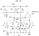
- FIG. 14 is a circuit diagram showing a configuration of a power-on reset circuit of a fifth comparative example.
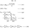
- FIG. 15 is a diagram for explaining an operation of the repower-on reset circuit illustrated in FIG. 14 .
- FIG. 16 is a circuit diagram showing a configuration of a current source used in the power-on reset circuit shown in FIG. 14 .
- a power-on reset circuit of a fifth comparative example includes PNP type bipolar transistors 91, 92, resistance elements 93 to 95, a comparator 99 composed of an operational amplifier, and PMOS transistors 96 to 98.
- the bipolar transistor 92 is formed by connecting N bipolar transistors in parallel.
- Each resistance value of the resistance elements 93, 95 is R 1
- a resistance value of the resistance element 94 is R 2 .
- the comparator 99 operates by a power-supply voltage (VCC).
- the bipolar transistor 91 and the PMOS transistor 96 are connected in series between a grounding node N91 that receives the grounding voltage (VSS) and a power-supply node N92 that receives the external power-supply voltage (VCC) in this order.
- a collector and a base of the bipolar transistor 91 are connected to the grounding node N91.
- An emitter of the bipolar transistor 91 is connected to a drain of the PMOS transistor 96, and its connecting point forms a node N93.
- a source of the PMOS transistor 96 is connected to the power-supply node N92.
- One end of the resistance element 93 is connected to the node N93, and the other end thereof is connected to the grounding node N91.
- the bipolar transistor 92, the resistance element 94, and the PMOS transistor 97 are connected in series between the grounding node N91 and the power-supply node N92 in this order.
- a collector and a base of the bipolar transistor 92 are connected to the grounding node N91.
- An emitter of the bipolar transistor 92 is connected to one end of the resistance element 94, and its connecting point forms a node N94.
- the other end of the resistance element 94 is connected to a drain of the PMOS transistor 97, and its connecting point forms a node N95.
- a source of the PMOS transistor 97 is connected to the power-supply node N92.
- One end of the resistance element 95 is connected to the node N95, and the other end thereof is connected to the grounding node N91.
- An inverting input terminal of the comparator 99 is connected to the node N95, and a non-inverting input terminal is connected to the node N93. It is detected that a voltage level of an output signal is inverted and the power-supply voltage (VCC) becomes (reaches) a predetermined voltage value (Vpor) when input voltages of the inverting input terminal and the non-inverting input terminal of the comparator 99 become the same voltage.
- VCC power-supply voltage
- Vpor predetermined voltage value
- V BE1 I A ⁇ R 2 + V BE2 and a first current (I A ) is represented by expression (21) shown in FIG. 15 .
- V BE1 is a base-emitter voltage of the bipolar transistor 91.
- V BE2 is a base-emitter voltage of the bipolar transistor 92.
- ⁇ V BE is a potential difference (V BE1 -V BE2 ) between the emitters of the bipolar transistor 91 and the bipolar transistor 92.
- kb represents the Boltzmann constant
- T represents absolute temperature
- q represents electron charge
- N represents the number of parallel connected bipolar transistors 92
- ln represents natural logarithm.
- a second current (I B ) is represented by expression (22) shown in FIG. 15 .
- a current flowing through the PMOS transistor 96 is the same as a current flowing through the PMOS transistor 98 as a current source, and is equal to the sum of the first current (I A ) and the second current (I B ). That is, a detection voltage (Vpor), which is the power-supply voltage (VCC) and which the comparator 99 reverses, is represented by expression (23) shown in FIG. 15 .
- R 3 is a resistance value defined by expression (26) shown in FIG. 16 .
- expression (24) shown in FIG. 15 can be obtained.
- a term M21 of expression (24) has a negative temperature characteristic
- a term M22 has a positive temperature characteristic. Therefore, by adding a voltage having the negative temperature characteristic and a voltage having the positive temperature characteristic, the added voltages are cancelled and can be detected with a voltage value having no temperature dependence.
- a current generating circuit includes resistance elements 101 to 103, a comparator 104 composed of an operational amplifier, and a PMOS transistor 98.
- the comparator 104 operates by the power-supply voltage (VCC).
- the resistance elements 101, 102 are connected in series between a grounding node N91 and a power-supply node N92 in this order.
- One end of the resistance element 101 is connected to the grounding node N91, the other end thereof is connected to one end of the resistance element 102, and its connecting point forms a node N101.
- the resistance element 103 and the PMOS transistor 98 are connected in series between the grounding node N91 and the power-supply node N92 in this order.
- One end of the resistance element 103 is connected to the grounding node N91, the other end thereof is connected to a drain of the PMOS transistor 98, and its connecting point forms a node N102.
- a source of the PMOS transistor 98 is connected to the power-supply node N92.
- An inverting input terminal of the comparator 104 is connected to the node N101, a non-inverting input terminal thereof is connected to the node N102, and an output terminal thereof is connected to a gate of the PMOS transistor 98.
- a current (I) generated by the current generating circuit as shown in FIG. 16 is represented by expression (26) shown in FIG. 16 . It is difficult to generate a current of 1 / R 3 shown in expression (26). That is, since resistor and capacitance are connected and adjusted so as not to oscillate an output, an area is increased and circuit design becomes complicated. In addition, variations in current increase several tens of times as much as variations in detection voltage. In addition, a lower voltage is difficult to detect since an operational lower limit is difficult to reduce. Furthermore, the consumed current is also difficult to reduce.
- FIG. 3 is a circuit diagram showing an example of a configuration of the power-on reset circuit illustrated in FIG. 1 .
- a power-on reset circuit 10 includes NPN type bipolar transistors 11, 12, resistance elements 13 to 18, a comparator 19 composed of an operational amplifier, and a PMOS transistor 20.
- the bipolar transistor 12 as a second bipolar transistor is formed by connecting N bipolar transistors in parallel.
- the comparator 19 operates by an external power-supply voltage (VCC).
- the resistance elements 13, 14, the bipolar transistor 11 as a first bipolar transistor, and a resistance element 15 are connected between a power-supply node N2 that receives the external power-supply voltage (VCC) and a grounding node N1 that receives the grounding voltage (GND) in this order.
- the grounding node N1 is also referred to as a first node
- the power-supply node N2 is also referred to as a second node.
- One end of the resistance element 13 as a fourth resistance element is connected to the power-supply node N2.
- the other end of the resistance element 13 is connected to one end of the resistance element 14 as a first resistance element, and its connecting point forms a node N3 as a third node.
- the other end of the resistance element 14 is connected to a collector of the bipolar transistor 11, and its connecting point forms a node N4 as a fourth node.
- An emitter of the bipolar transistor 11 is connected to one end of the resistance element 15 as a fifth resistance element, and its connecting point forms a node N6 as a sixth node.
- a base of the bipolar transistor 11 is connected to the node N3.
- One end of the resistance element 16 as a second resistance element is connected to a base (node N3) of the bipolar transistor 11, and the other end thereof is connected to the node N6.
- the resistance element 17 as a third resistance element and the bipolar transistor 12 are connected in series between the node N3 and the node N6 in this order.
- One end of the resistance element 17 is connected to the node N3.
- the other end of the resistance element 17 is connected to a collector of the bipolar transistor 12, and its connecting point forms a node N5.
- An emitter of the bipolar transistor 12 is connected to the node N6.
- Abase of the bipolar transistor 12 is connected to the node N4.
- the resistance elements 14, 17 are temperature-characteristic adjusting resistance elements, and its resistance value is R 1 .
- the resistance element 16 is a current adjusting resistance element, and its resistance value is R 2 .
- the resistance elements 13 and 15 are detection-voltage adjusting resistance elements, and each of their resistance values is R 3 .
- An inverting input terminal of the comparator 19 is connected to the node N5, a non-inverting input terminal thereof is connected to the node N4, and an output terminal thereof is connected to a gate of the PMOS transistor 20.
- the resistance element 18 and the PMOS transistor 20 are connected in series between the grounding node N1 and the power-supply node N2 in this order.
- One end of the resistance element 18 is connected to the grounding node N1.
- the other end of the resistance element 18 is connected to a drain of the PMOS transistor 20, and its connecting point forms an output node N7.
- a source of the PMOS transistor 20 is connected to the power-supply node N2.
- a reset signal (RS) is outputted from the output node N7.
- the resistance element 18 is a resistance element in order to ensure that the reset signal (RS) is outputted at the L level at a time of a lower voltage thereof.
- the output node N7 When the power-supply voltage (VCC) is 0 V, the output node N7 is maintained at 0 V. After power-on, a potential of the output node N7 is maintained at 0 V while a gate-source voltage of the PMOS transistor 20 is equal to or lower than a threshold voltage of the transistor. This state is the reset state. Thereafter, when the power-supply voltage (VCC) rises to a predetermined voltage and an output of the comparator 19 is inverted to the L level, a current driving force of the PMOS transistor 20 becomes larger than a current driving force of the resistance element 18 and a potential of the output node N7 rises and the reset state is released.
- VCC power-supply voltage
- FIG. 4 is a diagram for explaining an operation of the power-on reset circuit.
- the resistance element 14 is connected between the bipolar transistor 11 and the base of the bipolar transistor 12.
- V BE1 is a base-emitter voltage of the bipolar transistor 11.
- V BE2 is a base-emitter voltage of the bipolar transistor 12.
- the first current (I 1 ) is represented by expression (1) shown in FIG. 4 .
- ⁇ V BE represents each voltage of the resistance elements 14, 17.
- kb represents the Boltzmann constant
- T represents absolute temperature
- q represents electron charge
- N represents the number of parallel connected bipolar transistors 12
- ln represents natural logarithm.
- the first current (I 1 ) has a positive temperature characteristic in which a current value increases as temperature rises.
- the resistance element 16 is connected between the base and the emitter of the bipolar transistor 11.
- the second current (I 2 ) is generated in the resistance element 16 by a base-emitter voltage (V BE1 ).
- the second current (I 2 ) is represented by expression (2) shown in FIG. 4 .
- the second current (I 2 ) has a negative temperature characteristic in which a current value decreases as temperature rises.
- the resistance element 15 is connected to the grounding node N1, and the resistance element 13 is connected to the node N2.
- the power-supply voltage (VCC) becomes a voltage obtained by adding V BE1 and a voltage that is generated by the total current of the first current (I 1 ), the second current (I 2 ), and the third current (I 3 ) flowing through the resistance elements 13, 15.
- expression (4) shown in FIG. 4 can be obtained.
- a term M1 of expression (4) has a negative temperature characteristic
- a term M2 has a positive temperature characteristic. Therefore, by adding a voltage having a negative temperature characteristic and a voltage having a positive temperature characteristic, the added voltages are cancelled and can be detected with a voltage value having no temperature dependence.
- the resistance values (R 3 ) of the resistance elements 13, 15 are adjusted to become a detection voltage obtained by multiplying 1.2 V by (2R 3 / R 2 + 1). If the detection voltage has 1.2 V or more, it can be adjusted to a desired value.
- a detection-voltage equation in consideration of the offset effect is expression (5) shown in FIG. 4 , thereby being able to suppress its fluctuation by "In (N)” represented in "(1 / ln (N) -1) Vos" of an item M6 of expression (5).
- the power consumption of the power-on reset circuit 10 is about several hundred nA, which can be made smaller than about several ⁇ A of those in the third comparative example and the fifth comparative example. Further, the power-on reset circuit 10 does not require the reference-voltage generating circuit of the third comparative example, and does not require trimming control. Using the power-on reset circuit 10 makes it possible to lower an operation guaranteed voltage of the semiconductor device and to improve the battery life thereof.
- FIG. 5 is a circuit diagram showing another example of the configuration of the power-on reset circuit illustrated in FIG. 1 .
- the power-on reset circuit 10 may not have the resistance element 15 connected between the grounding node N1 and the node N6 shown in FIG. 3 . Further, the power-on reset circuit 10 may not have the resistance element 13 connected between the power-supply node N2 and the node N3 shown in FIG. 3 .
Landscapes
- Engineering & Computer Science (AREA)
- Physics & Mathematics (AREA)
- Theoretical Computer Science (AREA)
- General Physics & Mathematics (AREA)
- Nonlinear Science (AREA)
- Microelectronics & Electronic Packaging (AREA)
- General Engineering & Computer Science (AREA)
- Power Engineering (AREA)
- Electromagnetism (AREA)
- Radar, Positioning & Navigation (AREA)
- Automation & Control Theory (AREA)
- Electronic Switches (AREA)
Abstract
Description
- The present application claims priority from
Japanese Patent Application No. 2021-000625 filed on January 6, 2021 - The present disclosure relates to a semiconductor device, for example, is applicable to a semiconductor device having a power-on reset circuit.
- A power-on reset circuit is a circuit, which outputs a reset signal until a power-supply voltage has a predetermined value, in order that a system configured by another semiconductor device etc. or another circuit incorporated in the same semiconductor device is prevented from malfunctioning at power-on. Such a power-on reset circuit is disclosed in, for example,
Japanese patent application laid-open No. 2012-48349 Patent Document 1 and ELECTRONICS LETTERS 28th May 2015 V01. 51 No. 11 pp.856-858 as Non-PatentDocument 1. - In IoT (Internet of Things) equipment or the like, an improvement of battery life due to a reduction in an operational lower limit voltage of a semiconductor device and a reduction in consumed current are expected to advance in the further. Required is a detecting technique of a lower voltage of the power-on reset circuit that issues the reset signal at the operational lower limit voltage or less of the semiconductor device.
- Other problems and novel features will be apparent from the description of the present specification and the accompanied drawings.
- An outline of representative one of the present disclosures will briefly be described as follows.
- That is, a semiconductor device has a power-on reset circuit including: a first bipolar transistor; a second bipolar transistor configured by connecting a plurality of bipolar transistor in parallel; a detection-voltage adjusting resistance element; a temperature-characteristic adjusting resistance element; a current adjusting resistance element; and a comparator.
- According to the present disclosure, the power-on reset circuit can be made low voltage.
-
-
FIG. 1 is a block diagram showing a configuration of a semiconductor device according to an embodiment. -
FIG. 2 is a diagram for explaining a problem of a power-on reset circuit. -
FIG. 3 is a circuit diagram showing an example of a configuration of the power-on reset circuit illustrated inFIG. 1 . -
FIG. 4 is a diagram for explaining an operation of the power-on reset circuit illustrated inFIG. 3 . -
FIG. 5 is a circuit diagram showing another example of the configuration of the power-on reset circuit illustrated inFIG. 1 . -
FIG. 6 is a circuit diagram showing a configuration of a power-on reset circuit of a first comparative example. -
FIG. 7 is a diagram for explaining an operation of the power-on reset circuit illustrated inFIG. 6 . -
FIG. 8 is a circuit diagram showing a configuration of a power-on reset circuit of a second comparative example. -
FIG. 9 is a diagram for explaining of an operation of the power-on reset circuit illustrated inFIG. 8 . -
FIG. 10 is a view showing a configuration of a power-on reset circuit of a third comparative example. -
FIG. 11 is a diagram for explaining an operation of the power-on reset circuit illustrated inFIG. 10 . -
FIG. 12 is a circuit diagram showing a configuration of a power-on reset circuit of a fourth comparative example. -
FIG. 13 is a diagram for explaining an operation of the power-on reset circuit illustrated inFIG. 12 . -
FIG. 14 is a circuit diagram showing a configuration of a power-on reset circuit of a fifth comparative example. -
FIG. 15 is a diagram for explaining an operation of the power-on reset circuit illustrated inFIG. 14 . -
FIG. 16 is a circuit diagram showing a configuration of a current source used in the power-reset circuit illustrated inFIG. 14 . - Hereinafter, embodiments will be described with reference to the drawings. However, for the sake of clarification of the explanation, the following description and drawings will be omitted or simplified appropriately. Further, in the following description, the same components are denoted by the same reference numerals and a repetitive explanation thereof will be omitted.
-
FIG. 1 is a block diagram showing a configuration of a semiconductor device according to an embodiment. Asemiconductor device 1 is an integrated circuit (IC) in which a power-on reset circuit (POR) 10 and an internal circuit (INC) 30 are included in one semiconductor chip. When thesemiconductor device 1 is a microcontroller, theinternal circuit 30 includes a central processing unit (CPU), a RAM (Random Access Memory), peripheral circuits, and the like. Incidentally, the power-onreset circuit 10 is not built in thesemiconductor device 1, and may be formed on a semiconductor chip different from thesemiconductor device 1. - The power-on
reset circuit 10 outputs a reset signal (RS) to theinternal circuit 30 according to a value of a power-supply voltage (VCC) when power is turned on and when the power-supply voltage (VCC) temporarily drops and the like. When an external power-supply voltage (VCC) is lower than a predetermined voltage, the reset signal (RS) is at a low level (hereinafter referred to as L level), and when the external power-supply voltage (VCC) becomes higher than the predetermined voltage, the reset signal (RS) is switches to a high level (hereinafter referred to as H level). Here, the L level of the reset signal (RS) is called a reset state. The H level of the reset signal (RS) is called a release of the reset state. A specific example of the power-onreset circuit 10 will be described with reference toFIG. 3 . - Here, in order to further clarify the semiconductor device in the embodiment, a problem on the power-on
reset circuit 10 will be described with reference toFIGS. 2 ,6 and7 .FIG. 2 is a diagram for explaining a problem of a power-on reset circuit.FIG. 6 is a circuit diagram showing a configuration of a power-on reset circuit of a first comparative example.FIG. 7 is a diagram for explaining an operation of the power-on reset circuit illustrated inFIG. 6 . - As shown in
FIG. 6 , a power-on reset circuit of a first comparative example includes a PMOS (Positive Channel Metal Oxide Semiconductor)transistor 51, aresistance element 52, and abuffer circuit 53. ThePMOS transistor 51 and theresistance element 52 are provided in series between a power-supply-voltage (VCC) line and a grounding-voltage (GND) line in this order. A gate of thePMOS transistor 51 receives a grounding voltage (GND). A node between thePMOS transistor 51 and theresistance element 52 is connected to thebuffer circuit 53. Thebuffer circuit 53 outputs a reset signal (RS). - When the power-supply voltage (VCC) is 0 (zero) V, an intermediate potential node N51 is maintained at 0 V. After the power is turned on, a potential of the intermediate potential node N51 is maintained at 0 V while a gate-source voltage of the
PMOS transistor 51 is equal to or lower than a threshold voltage of the transistor. As shown inFIG. 7 , the reset signal (RS), which is an output of thebuffer circuit 53, is at the L level. This state is the reset state. Thereafter, when the power-supply voltage (VCC) rises to a predetermined voltage and a current driving force of thePMOS transistor 51 becomes larger than a current driving force of theresistance element 52, a potential of the intermediate potential node N51 rises. When the potential of the intermediate potential node N51 exceeds a threshold potential of thebuffer circuit 53, the reset signal (RS) becomes the H level and the reset state is released as shown inFIG. 7 . Here, the above-mentioned predetermined voltage is referred to as a detection voltage (Vpor). The power-on reset circuit has a detection circuit that detects a detection voltage (Vpor). - A battery power supply is discharged, and the power-supply voltage (VCC) drops with the passage of time. As a voltage of the
semiconductor device 1 drops, an operational lower limit voltage (VCCmin) drops as shown by an arrow (C) ofFIG. 2 , so that a battery life is improved and an operational time of thesemiconductor device 1 is extended as shown by an arrow (D) ofFIG. 2 . - As shown by (A) of
FIG. 2 , when the operational lower limit voltage (VCCmin) is VCC1, the power-onreset circuit 10 needs to detect the detection voltage (Vpor) at a voltage lower than that of VCC1. That is, the power-onreset circuit 10 needs to operate in a range from VCC1 of the power-supply voltage to VCC3 thereof. - By making the
semiconductor device 1 the lower voltage, as shown in (B) ofFIG. 2 , the power-onreset circuit 10 needs to detect the detection voltage (Vpor) at a voltage lower than the lower voltage (VCC2) . If the detection voltage (Vpor) cannot be lowered, the reset signal (RS) cannot be released as shown by a broken line inFIG. 7 . That is, the power-onreset circuit 10 needs to operate in a range from VCC2 of the power-supply voltage to VCC3 thereof. - Further, detection variations also need to be reduced as the detection voltage drops. Furthermore, in a battery-powered semiconductor device, a consumed current also needs to be reduced.
- Next, a power-on reset circuit of a second comparative example in which the detection variations of the detection voltage are reduced lower than those of the first comparative example will be described with reference to
FIGS. 8 and9 .FIG. 8 is a circuit diagram showing a configuration of a power-on reset circuit of a second comparative example.FIG. 9 is a diagram for explaining an operation of the power-on reset circuit illustrated inFIG. 8 . - As shown in
FIG. 8 , in a power-on reset circuit of a second comparative example, adetection circuit 62 for adjusting a detection voltage and a constant-current generating circuit 63 are added to the power-on reset circuit of the first comparative example. Thedetection circuit 62 includesPMOS transistors 54, 55 and an NMOS (Negative Channel Metal Oxide Semiconductor)transistor 56. ThePMOS transistors 54, 55 and theNMOS transistors 56 are connected in series between a power-supply-voltage (VCC) line and a grounding-voltage (VSS) line. Gates of thePMOS transistors PMOS transistor 54. The gate of the PMOS transistor 55 is connected to a drain of the PMOS transistor 55 to form a diode. A gate of theNMOS transistor 56 is connected to an output of the constant-current generating circuit 63. A current of a level corresponding to an output voltage of the constant-current generating circuit 63 flows through theNMOS transistor 56. - The constant-
current generating circuit 63 includesPMOS transistors NMOS transistors resistance element 61. ThePMOS transistor 57, theNMOS transistor 59, and theresistance element 61 are connected in series between a power-supply-voltage (VCC) line and a grounding-voltage (VSS) line. ThePMOS transistor 58 and theNMOS transistor 60 are connected in series between the power-supply-voltage (VCC) line and the grounding-voltage (VSS) line. Gates of thePMOS transistors PMOS transistor 58. Gates of theNMOS transistors NMOS transistor 59. A value of a constant current of the constant-current generating circuit 63 is determined by a difference between gate voltages of theNMOS transistors resistance element 61. At the output of the constant-current generating circuit 63, a bias voltage at a level corresponding to the constant current appears. - The resistance of the power-on reset circuits and the PMOS transistors in the first comparative example and the second comparative example have large process variations and temperature dependence. The variations of the power-on reset circuit in the second comparative example are smaller than those of the power-on reset circuit in the first comparative example, but the variations (ΔV) of the detection voltage are still about 600 mV. Therefore, as shown in
FIG. 9 , detection-voltage accuracy of the power-on reset circuits in the first comparative example and the second comparative example is considerably poor. Incidentally, power consumption of the power-on reset circuit in the second comparative example is about several hundred nA. - Moreover, it is difficult to set the detection voltage to about 1 V or more by using only the
resistance element 52 andPMOS transistor 51. Since the detection voltage is raised by Vth with a diode PMOS (PMOS transistor 55), it is difficult to adjust it up to a desired voltage. Therefore, it is difficult to adjust the detection voltages of the power-on reset circuits in the first comparative example and the second comparative example. - Next, a power-on reset circuit of a third comparative example in which the detection variations of the detection voltage are reduced lower than those of the second comparative example will be described with reference to
FIGS. 10 and11 .FIG. 10 is a view showing a configuration of a power-on reset circuit of a third comparative example.FIG. 11 is a diagram for explaining an operation of the power-on reset circuit illustrated inFIG. 10 . - A power-on reset circuit of a third comparative example includes a first power-on reset circuit (PORA) 64 and a second power-on reset circuit (PORB) 65. The first power-on reset circuit (PORA) 64 is composed of the power-on reset circuit of the first comparative example or the second comparative example, and a first reset signal (RSA) is outputted therefrom.
- The second power-on reset circuit (PORB) 65 includes
resistance elements resistance elements comparator 65c is connected to a connection node between theresistance elements comparator 65c. A second reset signal (RSB) is outputted from an output terminal of thecomparator 65c. When a detection voltage of the connection node exceeds the reference voltage (VR), the second reset signal (RSB) becomes the H level and the reset state is released. - Since the first power-on reset circuit (PORA) 64 is composed of the power-on reset circuit in the first comparative example or the second comparative example, as shown in
FIG. 11 , initial-rise variations of the first reset signal (RSA) are great. - The second power-on reset circuit (PORB) 65 can suppress initial rise variations of the second reset signal (RSB) by comparing the reference voltage (VR) and the power-supply voltage (VCC). However, as shown in
FIG. 11 , the second power-on reset circuit (PORB) 65 performs an indeterminate output until the bandgap reference circuit (BGR) 65d operates. Incidentally, the reference voltage (VR) at a time when the bandgap reference circuit (BGR) 65d is stable is about 1 V. - Therefore, at an operating voltage or less of the bandgap reference circuit (BGR) 65d, the second reset signal (RSB) is masked by the first reset signal (RSA) of the first power-on reset circuit (PORA) 64 in a
synthesis circuit 66, and compensates for an output of the L level. - In the power-on reset circuit of the third comparative example, the detection of the detection voltage (Vpor) can be set only to a value equal to or more than those of the operational lower limit voltage of the bandgap reference circuit (BGR) 65d and the detection variations of the first power-on reset circuit (PORA) 64. For example, the operational lower limit voltage of the bandgap reference circuit (BGR) 65d is about 1.5 V, and the detection variations of the first power-on reset circuit (PORA) 64 are about 0.6 V, so the detection voltage (Vpor) is 2 is detected near 2.1 V. Therefore, it is difficult for the power-on reset circuit in the third comparative example to detect a low voltage of the detection voltage (Vpor). Incidentally, the detection variations of the power-on reset circuit in the third comparative example are about 80 mV, which is improved so as to become higher than the detection-voltage accuracy of the power-on reset circuit in the second comparative example. However, the power consumption of the power-on reset circuit in the third comparative example is about several µA, which is higher than the power consumption of the power-on reset circuit in the second comparative example.
- Incidentally, the output of the bandgap reference circuit (BGR) 65d may be used as a reference voltage for other internal circuits, and the bandgap reference circuit (BGR) 65d may have a trimming function. At an initial rise of the power-supply voltage, a trimming value from a non-volatile memory such as a flash memory becomes indeterminate. Since the power-on reset circuit is used at the initial rise of power-on, trimming becomes indeterminate and the detection variations increase. Therefore, measures such as trimming and fixing needs to be taken so as not to be affected from such trimming's indeterminate state and increase in the variations.
- Next, a power-on reset circuit of a fourth comparative example for making the detection voltage lower will be described with reference to
FIGS. 12 and13 .FIG. 12 is a circuit diagram showing an example of a configuration of a power-on reset circuit of a fourth comparative example.FIG. 13 is a diagram for explaining an operation of the power-on reset circuit illustrated inFIG. 12 . - A power-on reset circuit of a fourth comparative example includes PNP type
bipolar transistors resistance elements 73 to 75, and acomparator 79 composed of an operational amplifier. Thebipolar transistor 72 is formed by connecting N bipolar transistors in parallel. Resistance values of theresistance elements resistance element 74 is R2. Thecomparator 79 operates by the power-supply voltage (VCC). First, connection between these components will be described. - The
bipolar transistor 71 and theresistance element 73 are connected in series between a grounding node N71 that receives the grounding voltage (VSS) and a power-supply node N72 that receives the external power-supply voltage (VCC) in this order. A collector and a base of thebipolar transistor 71 are connected to the grounding node N71. An emitter of thebipolar transistor 71 is connected to one end of theresistance element 73, and its connecting points forms a node N73. The other end of theresistance element 73 is connected to the power-supply node N72. - The
bipolar transistor 72 and theresistance elements bipolar transistor 72 are connected to the grounding node N71. An emitter of thebipolar transistor 72 is connected to one end of theresistance element 74, and its connecting point forms a node N74. The other end of theresistance element 74 is connected to one end of theresistance element 75, and its connecting point forms a node N74. The other end of theresistance element 75 is connected to the power-supply node N72. - The inverting input terminal of the
comparator 79 is connected to the node N74, and the non-inverting input terminal thereof is connected to the node N73. It is detected that a voltage level of the output signal is inverted and the power-supply voltage (VCC) becomes a predetermined voltage value (Vpor) when the input voltages of the inverting input terminal and the non-inverting input terminal of thecomparator 79 become the same voltage. At this time, a first current (I1) of theresistance elements resistance element 73 become equal to each other. - Since the voltage of the node N73 and the voltage of the node N74 are equal, VBE1 = I1 × R2 + VBE2 and the first current (I1) is represented by expression (11) shown in
FIG. 13 . Here, VBE1 is a base-emitter voltage of thebipolar transistor 71. VBE2 is a base-emitter voltage of thebipolar transistor 72. Further, since the second current (I2) is equal to the first current (I1), the second current (I2) is represented by expression (11) shown inFIG. 13 . - Further, a potential difference (VBE2 - VBE1) between the emitters of the
bipolar transistor 71 and thebipolar transistor 72 is represented by expression (12) shown inFIG. 13 . Here, kb represents the Boltzmann constant, T represents absolute temperature, q represents electron charge, N represents the number of parallel connectedbipolar transistors 72, and ln represents natural logarithm. - The power-supply voltage (VCC) is a voltage that is obtained by adding VBE1 and a voltage generated by the second current (I2) flowing through the
resistance element 73. That is, the detection voltage (Vpor) serving as the power-supply voltage (VCC), in which thecomparator 79 reverses, is represented by expression (13) shown inFIG. 13 . By substituting expression (11) into expression (13) shown inFIG. 6 , expression (14) shown inFIG. 13 can be obtained. Here, a term M11 of expression (14) has a negative temperature characteristic, and a term M12 has a positive temperature characteristic. Therefore, adding a voltage having the negative temperature characteristic and a voltage having the positive temperature characteristic make it possible to be canceled and be detected with a voltage value having no temperature dependence. - However, if resistance is adjusted so as to reduce the temperature dependence, a right side of expression (14) shown in
FIG. 13 becomes almost constant and the detection voltage (Vpor) can be set only near 1.2 V, so that the detection voltage cannot be adjusted. - Further, a detection-voltage equation considering an offset effect is expression (15) shown in
FIG. 13 , and when an offset (Vos) occurs in thecomparator 79, the offset becomes R1 / R2 times, thereby increasing the detection variations. In order to reduce the temperature dependence, the R1 / R2 needs to be set at about 10 times and, as a result, the offset increases 10 times. Therefore, the detection-voltage accuracy deteriorates. The detection variations of the power-on reset circuit in the fourth comparative example are about 130 mV, and the power consumption is about several hundred nA. - Next, a power-on reset circuit of a fifth comparative example, in which the detection voltage can be adjusted, will be described with reference to
FIGS. 14 to 16 .FIG. 14 is a circuit diagram showing a configuration of a power-on reset circuit of a fifth comparative example.FIG. 15 is a diagram for explaining an operation of the repower-on reset circuit illustrated inFIG. 14 .FIG. 16 is a circuit diagram showing a configuration of a current source used in the power-on reset circuit shown inFIG. 14 . - As shown in
FIG. 14 , a power-on reset circuit of a fifth comparative example includes PNP typebipolar transistors resistance elements 93 to 95, acomparator 99 composed of an operational amplifier, andPMOS transistors 96 to 98. Thebipolar transistor 92 is formed by connecting N bipolar transistors in parallel. Each resistance value of theresistance elements resistance element 94 is R2. Thecomparator 99 operates by a power-supply voltage (VCC). First, connection between these components will be described. - The
bipolar transistor 91 and thePMOS transistor 96 are connected in series between a grounding node N91 that receives the grounding voltage (VSS) and a power-supply node N92 that receives the external power-supply voltage (VCC) in this order. A collector and a base of thebipolar transistor 91 are connected to the grounding node N91. An emitter of thebipolar transistor 91 is connected to a drain of thePMOS transistor 96, and its connecting point forms a node N93. A source of thePMOS transistor 96 is connected to the power-supply node N92. One end of theresistance element 93 is connected to the node N93, and the other end thereof is connected to the grounding node N91. - The
bipolar transistor 92, theresistance element 94, and thePMOS transistor 97 are connected in series between the grounding node N91 and the power-supply node N92 in this order. A collector and a base of thebipolar transistor 92 are connected to the grounding node N91. An emitter of thebipolar transistor 92 is connected to one end of theresistance element 94, and its connecting point forms a node N94. The other end of theresistance element 94 is connected to a drain of thePMOS transistor 97, and its connecting point forms a node N95. A source of thePMOS transistor 97 is connected to the power-supply node N92. One end of theresistance element 95 is connected to the node N95, and the other end thereof is connected to the grounding node N91. - An inverting input terminal of the
comparator 99 is connected to the node N95, and a non-inverting input terminal is connected to the node N93. It is detected that a voltage level of an output signal is inverted and the power-supply voltage (VCC) becomes (reaches) a predetermined voltage value (Vpor) when input voltages of the inverting input terminal and the non-inverting input terminal of thecomparator 99 become the same voltage. - Since a voltage of the node N93 and a voltage of the node N94 are equal, VBE1 = IA × R2 + VBE2 and a first current (IA) is represented by expression (21) shown in
FIG. 15 . Here, VBE1 is a base-emitter voltage of thebipolar transistor 91. VBE2 is a base-emitter voltage of thebipolar transistor 92. ΔVBE is a potential difference (VBE1-VBE2) between the emitters of thebipolar transistor 91 and thebipolar transistor 92. Here, kb represents the Boltzmann constant, T represents absolute temperature, q represents electron charge, N represents the number of parallel connectedbipolar transistors 92, and ln represents natural logarithm. Further, a second current (IB) is represented by expression (22) shown inFIG. 15 . - A current flowing through the
PMOS transistor 96 is the same as a current flowing through thePMOS transistor 98 as a current source, and is equal to the sum of the first current (IA) and the second current (IB). That is, a detection voltage (Vpor), which is the power-supply voltage (VCC) and which thecomparator 99 reverses, is represented by expression (23) shown inFIG. 15 . Here, R3 is a resistance value defined by expression (26) shown inFIG. 16 . By substituting expressions (21) and (22) into expression (23) shown inFIG. 15 , expression (24) shown inFIG. 15 can be obtained. Here, a term M21 of expression (24) has a negative temperature characteristic, and a term M22 has a positive temperature characteristic. Therefore, by adding a voltage having the negative temperature characteristic and a voltage having the positive temperature characteristic, the added voltages are cancelled and can be detected with a voltage value having no temperature dependence. - However, a detection-voltage equation considering an offset effect is expression (25) shown in
FIG. 15 , and when an offset (Vos) occurs in thecomparator 79, the offset becomes (R3 / R1) × (R1 / R2) times to increase detection variations. When the detection voltage is about 2.4 V, R3 / R1 needs to be set at about 2 and R1 / R2 needs to be set at about 10 times in order to reduce the temperature dependence. As a result, the offset increases at 20 times. Therefore, the detection-voltage accuracy deteriorates. The detection variations of the power-on reset circuit in the fifth comparative example are about 130 mV, and the power consumption is about several µA. - Next, a current generating circuit of the power-on reset circuit shown in
FIG. 14 will be described with reference toFIG. 16 . A current generating circuit includesresistance elements 101 to 103, acomparator 104 composed of an operational amplifier, and aPMOS transistor 98. Thecomparator 104 operates by the power-supply voltage (VCC). - The
resistance elements resistance element 101 is connected to the grounding node N91, the other end thereof is connected to one end of theresistance element 102, and its connecting point forms a node N101. - The
resistance element 103 and thePMOS transistor 98 are connected in series between the grounding node N91 and the power-supply node N92 in this order. One end of theresistance element 103 is connected to the grounding node N91, the other end thereof is connected to a drain of thePMOS transistor 98, and its connecting point forms a node N102. A source of thePMOS transistor 98 is connected to the power-supply node N92. - An inverting input terminal of the
comparator 104 is connected to the node N101, a non-inverting input terminal thereof is connected to the node N102, and an output terminal thereof is connected to a gate of thePMOS transistor 98. - A current (I) generated by the current generating circuit as shown in
FIG. 16 is represented by expression (26) shown inFIG. 16 . It is difficult to generate a current of 1 / R3 shown in expression (26). That is, since resistor and capacitance are connected and adjusted so as not to oscillate an output, an area is increased and circuit design becomes complicated. In addition, variations in current increase several tens of times as much as variations in detection voltage. In addition, a lower voltage is difficult to detect since an operational lower limit is difficult to reduce. Furthermore, the consumed current is also difficult to reduce. - Next, a configuration of a power-on
reset circuit 10 of an embodiment will be described with reference toFIG. 3. FIG. 3 is a circuit diagram showing an example of a configuration of the power-on reset circuit illustrated inFIG. 1 . - A power-on
reset circuit 10 includes NPN typebipolar transistors resistance elements 13 to 18, acomparator 19 composed of an operational amplifier, and aPMOS transistor 20. Thebipolar transistor 12 as a second bipolar transistor is formed by connecting N bipolar transistors in parallel. Thecomparator 19 operates by an external power-supply voltage (VCC). First, connection between these components will be described. - The
resistance elements bipolar transistor 11 as a first bipolar transistor, and aresistance element 15 are connected between a power-supply node N2 that receives the external power-supply voltage (VCC) and a grounding node N1 that receives the grounding voltage (GND) in this order. Here, the grounding node N1 is also referred to as a first node, and the power-supply node N2 is also referred to as a second node. One end of theresistance element 13 as a fourth resistance element is connected to the power-supply node N2. The other end of theresistance element 13 is connected to one end of theresistance element 14 as a first resistance element, and its connecting point forms a node N3 as a third node. The other end of theresistance element 14 is connected to a collector of thebipolar transistor 11, and its connecting point forms a node N4 as a fourth node. An emitter of thebipolar transistor 11 is connected to one end of theresistance element 15 as a fifth resistance element, and its connecting point forms a node N6 as a sixth node. A base of thebipolar transistor 11 is connected to the node N3. - One end of the
resistance element 16 as a second resistance element is connected to a base (node N3) of thebipolar transistor 11, and the other end thereof is connected to the node N6. - The
resistance element 17 as a third resistance element and thebipolar transistor 12 are connected in series between the node N3 and the node N6 in this order. One end of theresistance element 17 is connected to the node N3. The other end of theresistance element 17 is connected to a collector of thebipolar transistor 12, and its connecting point forms a node N5. An emitter of thebipolar transistor 12 is connected to the node N6. Abase of thebipolar transistor 12 is connected to the node N4. - Here, the
resistance elements resistance element 16 is a current adjusting resistance element, and its resistance value is R2. Theresistance elements - An inverting input terminal of the
comparator 19 is connected to the node N5, a non-inverting input terminal thereof is connected to the node N4, and an output terminal thereof is connected to a gate of thePMOS transistor 20. - The
resistance element 18 and thePMOS transistor 20 are connected in series between the grounding node N1 and the power-supply node N2 in this order. One end of theresistance element 18 is connected to the grounding node N1. The other end of theresistance element 18 is connected to a drain of thePMOS transistor 20, and its connecting point forms an output node N7. A source of thePMOS transistor 20 is connected to the power-supply node N2. A reset signal (RS) is outputted from the output node N7. Here, theresistance element 18 is a resistance element in order to ensure that the reset signal (RS) is outputted at the L level at a time of a lower voltage thereof. - When the power-supply voltage (VCC) is 0 V, the output node N7 is maintained at 0 V. After power-on, a potential of the output node N7 is maintained at 0 V while a gate-source voltage of the
PMOS transistor 20 is equal to or lower than a threshold voltage of the transistor. This state is the reset state. Thereafter, when the power-supply voltage (VCC) rises to a predetermined voltage and an output of thecomparator 19 is inverted to the L level, a current driving force of thePMOS transistor 20 becomes larger than a current driving force of theresistance element 18 and a potential of the output node N7 rises and the reset state is released. - An operation of the power-on
reset circuit 10 will be described with reference toFIGS. 3 and4. FIG. 4 is a diagram for explaining an operation of the power-on reset circuit. - It is detected that a voltage level of an output signal is inverted and the power-supply voltage (VCC) becomes a detection voltage (Vpor) when input voltages of the inverting input terminal and the non-inverting input terminal of the
comparator 19 become the same voltage. At this time, a first current (I1) of theresistance element 14 and a third current (I3) of theresistance element 17 become equal. - The
resistance element 14 is connected between thebipolar transistor 11 and the base of thebipolar transistor 12. The first current (I1) is generated in theresistance element 14 by a potential difference (ΔVBE (= VBE2-VBE1)) between thebipolar transistor 11 and the base of thebipolar transistor 12. Here, VBE1 is a base-emitter voltage of thebipolar transistor 11. VBE2 is a base-emitter voltage of thebipolar transistor 12. - The first current (I1) is represented by expression (1) shown in
FIG. 4 . Here, ΔVBE represents each voltage of theresistance elements bipolar transistors 12, and ln represents natural logarithm. The first current (I1) has a positive temperature characteristic in which a current value increases as temperature rises. - The
resistance element 16 is connected between the base and the emitter of thebipolar transistor 11. The second current (I2) is generated in theresistance element 16 by a base-emitter voltage (VBE1). The second current (I2) is represented by expression (2) shown inFIG. 4 . The second current (I2) has a negative temperature characteristic in which a current value decreases as temperature rises. - The
resistance element 15 is connected to the grounding node N1, and theresistance element 13 is connected to the node N2. The power-supply voltage (VCC) becomes a voltage obtained by adding VBE1 and a voltage that is generated by the total current of the first current (I1), the second current (I2), and the third current (I3) flowing through theresistance elements - That is, the detection voltage (Vpor), which is the power-supply voltage (VCC) and which the
comparator 19 reverses, is represented by expression (3) shown inFIG. 4 . By substituting expressions (1) and (2) into expression (3) shown inFIG. 4 , expression (4) shown inFIG. 4 can be obtained. Here, a term M1 of expression (4) has a negative temperature characteristic, and a term M2 has a positive temperature characteristic. Therefore, by adding a voltage having a negative temperature characteristic and a voltage having a positive temperature characteristic, the added voltages are cancelled and can be detected with a voltage value having no temperature dependence. - Further, for example, it is assumed that the sum of the term M1 and the term M2 in expression (4) is 1.2 V, the resistance values (R3) of the
resistance elements - Furthermore, even if an offset (Vos) occurs in the
comparator 19, such an operation is performed as to be cancelled as described below and the variations in the detection voltage is suppressed. - When the current (I3) decreases due to the offset (Vos), the base-emitter voltage (VBE2) of the
bipolar transistor 12 drops. Consequently, the voltage (ΔVBE) of theresistance element 14 increases, and the first current (I1) increases. Therefore, such an operation is performed that the total current (I1 + I2 + I3) does not change. Since theresistance elements - A detection-voltage equation in consideration of the offset effect is expression (5) shown in
FIG. 4 , thereby being able to suppress its fluctuation by "In (N)" represented in "(1 / ln (N) -1) Vos" of an item M6 of expression (5). - For example, when the detection voltage is about 2.4 V, "(2R3 / R2 + 1)" of an item M3 in expression (5) is about 2. In order to reduce the temperature dependence, "(4R3 / R1 (2R3 / R2 + 1))" of the term M4 in expression (5) needs to be made about 10, so that the "2R3 / R1" of the term M5 in expression (5) becomes about 10. Since N, which is the number of parallel connected
bipolar transistors 12, is approximately 4 to 8, "(1 / ln (N) -1)" of the item M6 in expression (5) becomes 0.3 to 0.5, so that the detection variations increase by about 3 to 5 times of Vos. However, these detection variations can be made smaller 10 times than those of the fourth comparative example and 20 times than those of the fifth comparative example. Incidentally, the detection variations of the power-onreset circuit 10 is about 80 mV. - The power consumption of the power-on
reset circuit 10 is about several hundred nA, which can be made smaller than about several µA of those in the third comparative example and the fifth comparative example. Further, the power-onreset circuit 10 does not require the reference-voltage generating circuit of the third comparative example, and does not require trimming control. Using the power-onreset circuit 10 makes it possible to lower an operation guaranteed voltage of the semiconductor device and to improve the battery life thereof. - Another configuration of the power-on
reset circuit 10 will be described with reference toFIG. 5. FIG. 5 is a circuit diagram showing another example of the configuration of the power-on reset circuit illustrated inFIG. 1 . - As shown in
FIG. 5 , the power-onreset circuit 10 may not have theresistance element 15 connected between the grounding node N1 and the node N6 shown inFIG. 3 . Further, the power-onreset circuit 10 may not have theresistance element 13 connected between the power-supply node N2 and the node N3 shown inFIG. 3 . - The disclosure made by the present disclosers has been specifically described above based on the embodiment. The present disclosure is not limited to the above embodiment and, needless to say, can be variously modified or changed.
Claims (8)
- A semiconductor device having a power-on reset circuit, the power-on reset circuit comprising:a first bipolar transistor;a second bipolar transistor configured so that N bipolar transistors are connected in parallel;a comparator having an inverting input terminal, a non-inverting input terminal, and an output terminal;a first resistance element connected between a base of the first bipolar transistor and a base of the second bipolar transistor to generate a first current having a positive temperature characteristic in which a current value increases as temperature rises;a second resistance element connected between the base and an emitter of the first bipolar transistor to generate a second current having a negative temperature characteristic in which a current value decreases as temperature rises;a third resistance element connected between the base of the first bipolar transistor and the inverting input terminal to generate a third current having the positive temperature characteristic; anda fourth resistance element connected so as to carry a fourth current that is a total current of the first current, second current, and third current,wherein a collector of the first bipolar transistor and the base of the second bipolar transistor are connected to the non-inverting input terminal,wherein the power-on reset circuit is configured so that a voltage obtained by adding a voltage generated by the fourth current flowing in the fourth resistance element and a base-emitter voltage of the first bipolar transistor becomes a power-supply voltage, andwherein the power-on reset circuit is configured so that the comparator is reversed when the first current and the third current are equal to each other.
- The semiconductor device according to claim 1, further comprising:a PMOS transistor outputting a high level of the power-on reset circuit, the output terminal of the comparator being connected to a gate of the PMOS transistor; anda fifth resistance element connected to a drain of the PMOS transistor and outputting a low level of the power-on reset circuit.
- The semiconductor device according to claim 1 or 2,
wherein the fourth resistance element is connected to a power supply, and is connected to the first resistance element in series. - The semiconductor device according to any one of claims 1 to 3, further comprising an internal circuit receiving an output of the power-on reset circuit.
- A semiconductor device having a power-on reset circuit, the power-on reset circuit comprising:a first node supplying a reference voltage;a second node, a power-supply voltage is applied between the first node and the second node;a fourth resistance element, a first resistance element, and a first bipolar transistor connected in series between the second node and the first node;a third node connecting the fourth resistance element and the first resistance element;a fourth resistance element connecting the first resistance element and a collector of the first bipolar transistor;a second resistance element has one end connected to the third node and a base of the first bipolar transistor, and the other end connected to an emitter of the first bipolar transistor;a third resistance element and a second bipolar transistor connected in series between the third node and the first node;a fifth node connecting the third resistance and a collector of the second bipolar transistor; anda comparator having a non-inverting input terminal connecting the fourth node and an inverting input terminal connecting the fifth node,wherein the second bipolar transistor is configured so that N bipolar transistors are connected in parallel.
- The semiconductor device according to claim 5, further comprising a PMOS transistor and a fifth resistance element connected in series between the second node and the first node,wherein a source of the PMOS transistor is connected to the second node, and a gate thereof is connected to an output terminal of the comparator, andwherein one end of the fifth resistance element is connected to the first node, and the other end thereof is connected to a drain of the PMOS transistor.
- The semiconductor device according to claim 5 or 6, further comprising a sixth resistance element having one end connecting the first node, and the other end connected to an emitter of the first bipolar transistor and an emitter of the second bipolar transistor.
- The semiconductor device according to any one of claims 5 to 7, further comprising an internal circuit receiving an output of the power-on reset circuit.
Applications Claiming Priority (1)
| Application Number | Priority Date | Filing Date | Title |
|---|---|---|---|
| JP2021000625A JP7545901B2 (en) | 2021-01-06 | 2021-01-06 | Semiconductor Device |
Publications (2)
| Publication Number | Publication Date |
|---|---|
| EP4027521A1 true EP4027521A1 (en) | 2022-07-13 |
| EP4027521B1 EP4027521B1 (en) | 2024-12-18 |
Family
ID=79230911
Family Applications (1)
| Application Number | Title | Priority Date | Filing Date |
|---|---|---|---|
| EP22150320.4A Active EP4027521B1 (en) | 2021-01-06 | 2022-01-05 | Semiconductor device |
Country Status (4)
| Country | Link |
|---|---|
| US (1) | US11646731B2 (en) |
| EP (1) | EP4027521B1 (en) |
| JP (1) | JP7545901B2 (en) |
| CN (1) | CN114726352A (en) |
Families Citing this family (1)
| Publication number | Priority date | Publication date | Assignee | Title |
|---|---|---|---|---|
| JP7494610B2 (en) * | 2020-07-10 | 2024-06-04 | セイコーエプソン株式会社 | Circuit device and real-time clock device |
Citations (4)
| Publication number | Priority date | Publication date | Assignee | Title |
|---|---|---|---|---|
| FR2844118A1 (en) * | 2002-08-29 | 2004-03-05 | St Microelectronics Sa | An electronic circuit for detecting a supply potential as having a sufficient value after switching on, for use in integrated circuit devices such as chip cards |
| JP2012048349A (en) | 2010-08-25 | 2012-03-08 | Renesas Electronics Corp | Semiconductor device |
| US20120212194A1 (en) * | 2011-02-23 | 2012-08-23 | Fujitsu Semiconductor Limited | Reference voltage circuit and semiconductor integrated circuit |
| WO2020165250A1 (en) * | 2019-02-12 | 2020-08-20 | Ams International Ag | Threshold detector of a power on reset circuit with improved accuracy for switching levels over temperature variations |
Family Cites Families (11)
| Publication number | Priority date | Publication date | Assignee | Title |
|---|---|---|---|---|
| US6642777B2 (en) | 2001-07-05 | 2003-11-04 | Texas Instruments Incorporated | Voltage reference circuit with increased intrinsic accuracy |
| US6559629B1 (en) | 2001-07-09 | 2003-05-06 | Cygnal Integrated Products, Inc. | Supply voltage monitor using bandgap device without feedback |
| KR101072611B1 (en) | 2003-05-23 | 2011-10-11 | 페어차일드코리아반도체 주식회사 | Temperature-Independent Current Supply Circuit |
| JP2007060544A (en) | 2005-08-26 | 2007-03-08 | Micron Technol Inc | Method and apparatus for generating power on reset with low temperature coefficient |
| US7919999B2 (en) | 2007-10-18 | 2011-04-05 | Micron Technology, Inc. | Band-gap reference voltage detection circuit |
| US7876135B2 (en) * | 2008-02-29 | 2011-01-25 | Spectra Linear, Inc. | Power-on reset circuit |
| EP2698681B1 (en) * | 2011-04-12 | 2023-03-29 | Renesas Electronics Corporation | Voltage generating circuit |
| CN102624369B (en) | 2012-01-12 | 2014-10-29 | 苏州华芯微电子股份有限公司 | POR (Power-on Reset) circuit with variable reset point on basis of band gap reference source |
| US20150042386A1 (en) * | 2013-08-06 | 2015-02-12 | Cirel Systems Private Limited | Highly accurate power-on reset circuit with least delay |
| US9606563B2 (en) * | 2014-04-08 | 2017-03-28 | Texas Instruments Deutschland Gmbh | Bandgap reference voltage failure detection |
| JP7251929B2 (en) | 2018-06-21 | 2023-04-04 | ラピスセミコンダクタ株式会社 | Semiconductor device and power-on reset signal generation method |
-
2021
- 2021-01-06 JP JP2021000625A patent/JP7545901B2/en active Active
- 2021-12-23 US US17/560,671 patent/US11646731B2/en active Active
- 2021-12-31 CN CN202111661676.1A patent/CN114726352A/en active Pending
-
2022
- 2022-01-05 EP EP22150320.4A patent/EP4027521B1/en active Active
Patent Citations (4)
| Publication number | Priority date | Publication date | Assignee | Title |
|---|---|---|---|---|
| FR2844118A1 (en) * | 2002-08-29 | 2004-03-05 | St Microelectronics Sa | An electronic circuit for detecting a supply potential as having a sufficient value after switching on, for use in integrated circuit devices such as chip cards |
| JP2012048349A (en) | 2010-08-25 | 2012-03-08 | Renesas Electronics Corp | Semiconductor device |
| US20120212194A1 (en) * | 2011-02-23 | 2012-08-23 | Fujitsu Semiconductor Limited | Reference voltage circuit and semiconductor integrated circuit |
| WO2020165250A1 (en) * | 2019-02-12 | 2020-08-20 | Ams International Ag | Threshold detector of a power on reset circuit with improved accuracy for switching levels over temperature variations |
Non-Patent Citations (1)
| Title |
|---|
| ELECTRONICS LETTERS, 28 May 2015 (2015-05-28), pages 856 - 858 |
Also Published As
| Publication number | Publication date |
|---|---|
| US20220216866A1 (en) | 2022-07-07 |
| JP7545901B2 (en) | 2024-09-05 |
| JP2022106004A (en) | 2022-07-19 |
| CN114726352A (en) | 2022-07-08 |
| EP4027521B1 (en) | 2024-12-18 |
| US11646731B2 (en) | 2023-05-09 |
Similar Documents
| Publication | Publication Date | Title |
|---|---|---|
| US6882213B2 (en) | Temperature detection circuit insensitive to power supply voltage and temperature variation | |
| JP5215995B2 (en) | Ultra-low power analog compensation circuit | |
| US9515637B1 (en) | Power-on reset circuit | |
| US9136827B2 (en) | Power-on reset circuit | |
| US8593887B2 (en) | Semiconductor device having reference voltage generating unit | |
| CN103378830A (en) | Power-on reset (POR) circuit | |
| US20180375511A9 (en) | Power-on reset circuit | |
| US7642840B2 (en) | Reference voltage generator circuit | |
| US11705902B2 (en) | Supply voltage detecting circuit and circuit system using the same | |
| EP4027521B1 (en) | Semiconductor device | |
| CN110739943A (en) | reset circuit with temperature compensation | |
| US6400207B1 (en) | Quick turn-on disable/enable bias control circuit for high speed CMOS opamp | |
| US7190212B2 (en) | Power-up and BGREF circuitry | |
| CN116633116B (en) | Low-power consumption current source, current source circuit, chip and electronic equipment with low-power consumption current source circuit | |
| JP2011188361A (en) | Power-on reset circuit | |
| CN112286337A (en) | Low-power-consumption bandgap circuit for MCU and implementation method thereof | |
| US9437258B2 (en) | Data readout circuit of a storage device for read-out operation for preventing erroneous writing into a data storage element and reading out of the data correctly | |
| US11296692B1 (en) | Power-on reset circuit | |
| CN115903992A (en) | Voltage generating circuit and semiconductor device | |
| CN114610108A (en) | Bias current generating circuit | |
| CN218525041U (en) | Over-temperature detection circuit, linear voltage regulator, chip and electronic equipment | |
| CN112650345B (en) | Semiconductor device with a plurality of semiconductor chips | |
| JPH09186294A (en) | Voltage generation circuit and semiconductor device | |
| CN116346101B (en) | Reset circuit, reset signal generation method and chip | |
| CN118731455A (en) | A voltage detection circuit for signal transmission link |
Legal Events
| Date | Code | Title | Description |
|---|---|---|---|
| PUAI | Public reference made under article 153(3) epc to a published international application that has entered the european phase |
Free format text: ORIGINAL CODE: 0009012 |
|
| STAA | Information on the status of an ep patent application or granted ep patent |
Free format text: STATUS: THE APPLICATION HAS BEEN PUBLISHED |
|
| AK | Designated contracting states |
Kind code of ref document: A1 Designated state(s): AL AT BE BG CH CY CZ DE DK EE ES FI FR GB GR HR HU IE IS IT LI LT LU LV MC MK MT NL NO PL PT RO RS SE SI SK SM TR |
|
| STAA | Information on the status of an ep patent application or granted ep patent |
Free format text: STATUS: REQUEST FOR EXAMINATION WAS MADE |
|
| 17P | Request for examination filed |
Effective date: 20221229 |
|
| RBV | Designated contracting states (corrected) |
Designated state(s): AL AT BE BG CH CY CZ DE DK EE ES FI FR GB GR HR HU IE IS IT LI LT LU LV MC MK MT NL NO PL PT RO RS SE SI SK SM TR |
|
| GRAP | Despatch of communication of intention to grant a patent |
Free format text: ORIGINAL CODE: EPIDOSNIGR1 |
|
| STAA | Information on the status of an ep patent application or granted ep patent |
Free format text: STATUS: GRANT OF PATENT IS INTENDED |
|
| INTG | Intention to grant announced |
Effective date: 20240709 |
|
| RIN1 | Information on inventor provided before grant (corrected) |
Inventor name: TSUDA, ATSUSHI Inventor name: KASHIMA, ISSEI |
|
| GRAS | Grant fee paid |
Free format text: ORIGINAL CODE: EPIDOSNIGR3 |
|
| GRAA | (expected) grant |
Free format text: ORIGINAL CODE: 0009210 |
|
| STAA | Information on the status of an ep patent application or granted ep patent |
Free format text: STATUS: THE PATENT HAS BEEN GRANTED |
|
| AK | Designated contracting states |
Kind code of ref document: B1 Designated state(s): AL AT BE BG CH CY CZ DE DK EE ES FI FR GB GR HR HU IE IS IT LI LT LU LV MC MK MT NL NO PL PT RO RS SE SI SK SM TR |
|
| REG | Reference to a national code |
Ref country code: CH Ref legal event code: EP |
|
| REG | Reference to a national code |
Ref country code: DE Ref legal event code: R096 Ref document number: 602022008688 Country of ref document: DE |
|
| REG | Reference to a national code |
Ref country code: IE Ref legal event code: FG4D |
|
| REG | Reference to a national code |
Ref country code: LT Ref legal event code: MG9D |
|
| PG25 | Lapsed in a contracting state [announced via postgrant information from national office to epo] |
Ref country code: HR Free format text: LAPSE BECAUSE OF FAILURE TO SUBMIT A TRANSLATION OF THE DESCRIPTION OR TO PAY THE FEE WITHIN THE PRESCRIBED TIME-LIMIT Effective date: 20241218 |
|
| PG25 | Lapsed in a contracting state [announced via postgrant information from national office to epo] |
Ref country code: FI Free format text: LAPSE BECAUSE OF FAILURE TO SUBMIT A TRANSLATION OF THE DESCRIPTION OR TO PAY THE FEE WITHIN THE PRESCRIBED TIME-LIMIT Effective date: 20241218 |
|
| PG25 | Lapsed in a contracting state [announced via postgrant information from national office to epo] |
Ref country code: BG Free format text: LAPSE BECAUSE OF FAILURE TO SUBMIT A TRANSLATION OF THE DESCRIPTION OR TO PAY THE FEE WITHIN THE PRESCRIBED TIME-LIMIT Effective date: 20241218 |
|
| PG25 | Lapsed in a contracting state [announced via postgrant information from national office to epo] |
Ref country code: NO Free format text: LAPSE BECAUSE OF FAILURE TO SUBMIT A TRANSLATION OF THE DESCRIPTION OR TO PAY THE FEE WITHIN THE PRESCRIBED TIME-LIMIT Effective date: 20250318 |
|
| REG | Reference to a national code |
Ref country code: NL Ref legal event code: MP Effective date: 20241218 |
|
| PG25 | Lapsed in a contracting state [announced via postgrant information from national office to epo] |
Ref country code: LV Free format text: LAPSE BECAUSE OF FAILURE TO SUBMIT A TRANSLATION OF THE DESCRIPTION OR TO PAY THE FEE WITHIN THE PRESCRIBED TIME-LIMIT Effective date: 20241218 Ref country code: GR Free format text: LAPSE BECAUSE OF FAILURE TO SUBMIT A TRANSLATION OF THE DESCRIPTION OR TO PAY THE FEE WITHIN THE PRESCRIBED TIME-LIMIT Effective date: 20250319 |
|
| PG25 | Lapsed in a contracting state [announced via postgrant information from national office to epo] |
Ref country code: RS Free format text: LAPSE BECAUSE OF FAILURE TO SUBMIT A TRANSLATION OF THE DESCRIPTION OR TO PAY THE FEE WITHIN THE PRESCRIBED TIME-LIMIT Effective date: 20250318 |
|
| PG25 | Lapsed in a contracting state [announced via postgrant information from national office to epo] |
Ref country code: NL Free format text: LAPSE BECAUSE OF FAILURE TO SUBMIT A TRANSLATION OF THE DESCRIPTION OR TO PAY THE FEE WITHIN THE PRESCRIBED TIME-LIMIT Effective date: 20241218 |
|
| REG | Reference to a national code |
Ref country code: AT Ref legal event code: MK05 Ref document number: 1753072 Country of ref document: AT Kind code of ref document: T Effective date: 20241218 |
|
| PG25 | Lapsed in a contracting state [announced via postgrant information from national office to epo] |
Ref country code: SM Free format text: LAPSE BECAUSE OF FAILURE TO SUBMIT A TRANSLATION OF THE DESCRIPTION OR TO PAY THE FEE WITHIN THE PRESCRIBED TIME-LIMIT Effective date: 20241218 |
|
| PG25 | Lapsed in a contracting state [announced via postgrant information from national office to epo] |
Ref country code: PL Free format text: LAPSE BECAUSE OF FAILURE TO SUBMIT A TRANSLATION OF THE DESCRIPTION OR TO PAY THE FEE WITHIN THE PRESCRIBED TIME-LIMIT Effective date: 20241218 |
|
| PG25 | Lapsed in a contracting state [announced via postgrant information from national office to epo] |
Ref country code: ES Free format text: LAPSE BECAUSE OF FAILURE TO SUBMIT A TRANSLATION OF THE DESCRIPTION OR TO PAY THE FEE WITHIN THE PRESCRIBED TIME-LIMIT Effective date: 20241218 |
|
| PG25 | Lapsed in a contracting state [announced via postgrant information from national office to epo] |
Ref country code: IS Free format text: LAPSE BECAUSE OF FAILURE TO SUBMIT A TRANSLATION OF THE DESCRIPTION OR TO PAY THE FEE WITHIN THE PRESCRIBED TIME-LIMIT Effective date: 20250418 |
|
| PG25 | Lapsed in a contracting state [announced via postgrant information from national office to epo] |
Ref country code: PT Free format text: LAPSE BECAUSE OF FAILURE TO SUBMIT A TRANSLATION OF THE DESCRIPTION OR TO PAY THE FEE WITHIN THE PRESCRIBED TIME-LIMIT Effective date: 20250421 |
|
| PG25 | Lapsed in a contracting state [announced via postgrant information from national office to epo] |
Ref country code: EE Free format text: LAPSE BECAUSE OF FAILURE TO SUBMIT A TRANSLATION OF THE DESCRIPTION OR TO PAY THE FEE WITHIN THE PRESCRIBED TIME-LIMIT Effective date: 20241218 |
|
| PG25 | Lapsed in a contracting state [announced via postgrant information from national office to epo] |
Ref country code: RO Free format text: LAPSE BECAUSE OF FAILURE TO SUBMIT A TRANSLATION OF THE DESCRIPTION OR TO PAY THE FEE WITHIN THE PRESCRIBED TIME-LIMIT Effective date: 20241218 Ref country code: AT Free format text: LAPSE BECAUSE OF FAILURE TO SUBMIT A TRANSLATION OF THE DESCRIPTION OR TO PAY THE FEE WITHIN THE PRESCRIBED TIME-LIMIT Effective date: 20241218 |
|
| PG25 | Lapsed in a contracting state [announced via postgrant information from national office to epo] |
Ref country code: SK Free format text: LAPSE BECAUSE OF FAILURE TO SUBMIT A TRANSLATION OF THE DESCRIPTION OR TO PAY THE FEE WITHIN THE PRESCRIBED TIME-LIMIT Effective date: 20241218 |
|
| PG25 | Lapsed in a contracting state [announced via postgrant information from national office to epo] |
Ref country code: CZ Free format text: LAPSE BECAUSE OF FAILURE TO SUBMIT A TRANSLATION OF THE DESCRIPTION OR TO PAY THE FEE WITHIN THE PRESCRIBED TIME-LIMIT Effective date: 20241218 |
|
| PG25 | Lapsed in a contracting state [announced via postgrant information from national office to epo] |
Ref country code: IT Free format text: LAPSE BECAUSE OF FAILURE TO SUBMIT A TRANSLATION OF THE DESCRIPTION OR TO PAY THE FEE WITHIN THE PRESCRIBED TIME-LIMIT Effective date: 20241218 |
|
| REG | Reference to a national code |
Ref country code: CH Ref legal event code: PL |
|
| PG25 | Lapsed in a contracting state [announced via postgrant information from national office to epo] |
Ref country code: SE Free format text: LAPSE BECAUSE OF FAILURE TO SUBMIT A TRANSLATION OF THE DESCRIPTION OR TO PAY THE FEE WITHIN THE PRESCRIBED TIME-LIMIT Effective date: 20241218 |
|
| PG25 | Lapsed in a contracting state [announced via postgrant information from national office to epo] |
Ref country code: MC Free format text: LAPSE BECAUSE OF FAILURE TO SUBMIT A TRANSLATION OF THE DESCRIPTION OR TO PAY THE FEE WITHIN THE PRESCRIBED TIME-LIMIT Effective date: 20241218 Ref country code: LU Free format text: LAPSE BECAUSE OF NON-PAYMENT OF DUE FEES Effective date: 20250105 |
|
| REG | Reference to a national code |
Ref country code: DE Ref legal event code: R097 Ref document number: 602022008688 Country of ref document: DE |
|
| PG25 | Lapsed in a contracting state [announced via postgrant information from national office to epo] |
Ref country code: DK Free format text: LAPSE BECAUSE OF FAILURE TO SUBMIT A TRANSLATION OF THE DESCRIPTION OR TO PAY THE FEE WITHIN THE PRESCRIBED TIME-LIMIT Effective date: 20241218 |
|
| PG25 | Lapsed in a contracting state [announced via postgrant information from national office to epo] |
Ref country code: BE Free format text: LAPSE BECAUSE OF NON-PAYMENT OF DUE FEES Effective date: 20250131 |
|
| PG25 | Lapsed in a contracting state [announced via postgrant information from national office to epo] |
Ref country code: CH Free format text: LAPSE BECAUSE OF NON-PAYMENT OF DUE FEES Effective date: 20250131 |
|
| REG | Reference to a national code |
Ref country code: BE Ref legal event code: MM Effective date: 20250131 |
|
| PLBE | No opposition filed within time limit |
Free format text: ORIGINAL CODE: 0009261 |
|
| STAA | Information on the status of an ep patent application or granted ep patent |
Free format text: STATUS: NO OPPOSITION FILED WITHIN TIME LIMIT |
|
| 26N | No opposition filed |
Effective date: 20250919 |
|
| PG25 | Lapsed in a contracting state [announced via postgrant information from national office to epo] |
Ref country code: FR Free format text: LAPSE BECAUSE OF NON-PAYMENT OF DUE FEES Effective date: 20250218 |
|
| PG25 | Lapsed in a contracting state [announced via postgrant information from national office to epo] |
Ref country code: IE Free format text: LAPSE BECAUSE OF NON-PAYMENT OF DUE FEES Effective date: 20250105 |
|
| PGFP | Annual fee paid to national office [announced via postgrant information from national office to epo] |
Ref country code: DE Payment date: 20260127 Year of fee payment: 5 |